
REV. B
Information furnished by Analog Devices is believed to be accurate and
reliable. However, no responsibility is assumed by Analog Devices for its
use, nor for any infringements of patents or other rights of third parties that
may result from its use. No license is granted by implication or otherwise
under any patent or patent rights of Analog Devices.
a
AD711
One Technology Way, P.O. Box 9106, Norwood, MA 02062-9106, U.S.A.
Tel: 781/329-4700
www.analog.com
Fax: 781/326-8703
© Analog Devices, Inc., 2002
Precision, LowCost,
High Speed, BiFET Op Amp
FEATURES
Enhanced Replacement for LF411 and TL081
AC PERFORMANCE
Settles to 0.01% in 1.0 s
16 V/ s min Slew Rate (AD711J)
3 MHz min Unity Gain Bandwidth (AD711J)
DC PERFORMANCE
0.25 mV max Offset Voltage: (AD711C)
3 V/ C max Drift: (AD711C)
200 V/mV min Open-Loop Gain (AD711K)
4 V p-p max Noise, 0.1 Hz to 10 Hz (AD711C)
Available in Plastic Mini-DIP, Plastic SO, Hermetic
Cerdip, and Hermetic Metal Can Packages
MIL-STD-883B Parts Available
Available in Tape and Reel in Accordance with
EIA-481A Standard
Surface Mount (SOIC)
Dual Version: AD712
PRODUCT DESCRIPTION
The AD711 is a high speed, precision monolithic operational
amplifier offering high performance at very modest prices. Its
very low offset voltage and offset voltage drift are the results of
advanced laser wafer trimming technology. These performance
benefits allow the user to easily upgrade existing designs that use
older precision BiFETs and, in many cases, bipolar op amps.
The superior ac and dc performance of this op amp makes it
suitable for active filter applications. With a slew rate of 16 V/
µs
and a settling time of 1
µs to ±0.01%, the AD711 is ideal as a
buffer for 12-bit D/A and A/D Converters and as a high-speed
integrator. The settling time is unmatched by any similar IC
amplifier.
The combination of excellent noise performance and low input
current also make the AD711 useful for photo diode preamps.
Common-mode rejection of 88 dB and open loop gain of
400 V/mV ensure 12-bit performance even in high-speed unity
gain buffer circuits.
The AD711 is pinned out in a standard op amp configuration
and is available in seven performance grades. The AD711J and
AD711K are rated over the commercial temperature range of
0
°C to 70°C. The AD711A, AD711B and AD711C are rated
over the industrial temperature range of 40
°C to +85°C. The
AD711S and AD711T are rated over the military temperature
range of 40
°C to +125°C and are available processed to MIL-
STD-883B, Rev. C.
Extended reliability PLUS screening is available, specified over
the commercial and industrial temperature ranges. PLUS
screening includes 168 hour burn-in, as well as other environ-
mental and physical tests.
The AD711 is available in an 8-pin plastic mini-DIP, small
outline, cerdip, TO-99 metal can, or in chip form.
PRODUCT HIGHLIGHTS
1. The AD711 offers excellent overall performance at very
competitive prices.
2. Analog Devices' advanced processing technology and 100%
testing guarantee a low input offset voltage (0.25 mV max,
C grade, 2 mV max, J grade). Input offset voltage is specified
in the warmed-up condition. Analog Devices' laser wafer
drift trimming process reduces input offset voltage drifts to
3
µV/°C max on the AD711C.
3. Along with precision dc performance, the AD711 offers
excellent dynamic response. It settles to
±0.01% in 1 µs and
has a 100% tested minimum slew rate of 16 V/
µs. Thus this
device is ideal for applications such as DAC and ADC
buffers which require a combination of superior ac and dc
performance.
4. The AD711 has a guaranteed and tested maximum voltage
noise of 4
µV p-p, 0.1 to 10 Hz (AD711C).
5. Analog Devices' well-matched, ion-implanted JFETs ensure
a guaranteed input bias current (at either input) of 25 pA
max (AD711C) and an input offset current of 10 pA max
(AD711C). Both input bias current and input offset current
are guaranteed in the warmed-up condition.
CONNECTION DIAGRAMS
8
7
6
5
1
2
3
4
NC = NO CONNECT
OFFSET
NULL
NC
OUTPUT
AD711
INVERTING
INPUT
NONINVERTING
INPUT
V
S
+V
S
OFFSET
NULL
10k
V
OS
TRIM
15V
NC
OFFSET
NULL
INVERTING
INPUT
NON
INVERTING
INPUT
OFFSET
NULL
OUTPUT
V
S
+V
S
NC = NO CONNECT
AD711
NOTE
PIN 4 CONNECTED TO CASE

REV. B
2
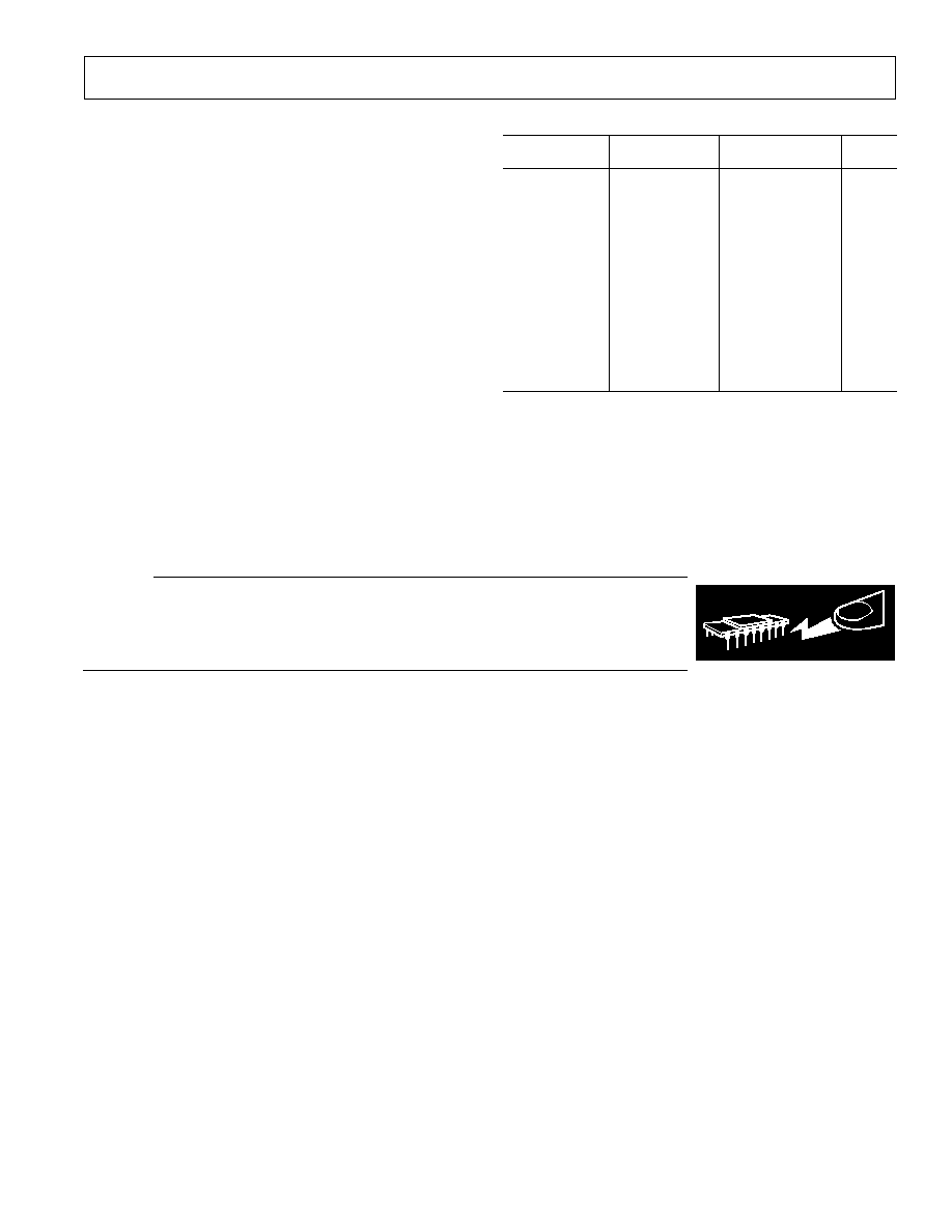
AD711SPECIFICATIONS
(V
S
= 15
V @ T
A
= 25 C, unless otherwise noted.)
J/A/S
K/B/T
C
Parameter
Min
Typ
Max
Min
Typ
Max
Min
Typ
Max
Unit
INPUT OFFSET VOLTAGE
1
Initial Offset
0.3
2/1/1
0.2
0.5
0.10
0.25
mV
T
MIN
to T
MAX
3/2/2
1.0
0.45
mV
vs. Temp
7
20/20/20
5
10
2
5
µV/°C
vs. Supply
76
95
80
100
86
110
dB
T
MIN
to T
MAX
76/76/76
80
86
dB
Long-Term Stability
15
15
15
µV/Month
INPUT BIAS CURRENT
2
V
CM
= 0 V
15
50
15
50
15
25
pA
V
CM
= 0 V @ T
MAX
1.1/3.2/51
1.1/3.2/51
1.6
nA
V
CM
=
±10 V
20
100
20
100
20
50
pA
INPUT OFFSET CURRENT
V
CM
= 0 V
10
25
5
25
5
10
pA
V
CM
= 0 V @ T
MAX
0.6/1.6/26
0.6/1.6/26
0.65
nA
FREQUENCY RESPONSE
Small Signal Bandwidth
3.0
4.0
3.4
4.0
3.4
4.0
MHz
Full Power Response
200
200
200
kHz
Slew Rate
16
20
18
20
18
20
V/
µs
Settling Time to 0.01%
1.0
1.2
1.0
1.2
1.0
1.2
µs
Total Harmonic Distortion
0.0003
0.0003
0.0003
%
INPUT IMPEDANCE
Differential
3
× 10
12
5.5
3
× 10
12
5.5
3
× 10
12
5.5
pF
Common Mode
3
× 10
12
5.5
3
× 10
12
5.5
3
× 10
12
5.5
pF
INPUT VOLTAGE RANGE
Differential
3
±20
±20
±20
V
Common-Mode Voltage
4
+14.5, 11.5
+14.5, 11.5
+14.5, 11.5
T
MIN
to T
MAX
V
S
+ 4
+V
S
2
V
S
+ 4
+V
S
2
V
S
+ 4
+V
2 V
Common-Mode
Rejection Ratio
V
CM
=
±10 V
76
88
80
88
86
94
dB
T
MIN
to T
MAX
76/76/76
84
80
84
86
90
dB
V
CM
=
±11 V
70
84
76
84
76
90
dB
T
MIN
to T
MAX
70/70/70
80
74
80
74
84
dB
INPUT VOLTAGE NOISE
2
2
2
4
µV p-p
45
45
45
nV/
Hz
22
22
22
nV/
Hz
18
18
18
nV/
Hz
16
16
16
nV/
Hz
INPUT CURRENT NOISE
0.01
0.01
0.01
pA/
Hz
OPEN-LOOP GAIN
150
400
200
400
200
400
V/mV
100/100/100
100
100
V/mV
OUTPUT
CHARACTERISTICS
Voltage
+13, 12.5
+13.9, 13.3
+13, 12.5 +13.9, 13.3
+13, 12.5 +13.9, 13.3
V
±12/±12/±12 +13.8, 13.1
±12
+13.8, 13.1
±12
+13.8, 13.1
V
Current
25
25
25
mA
POWER SUPPLY
Rated Performance
±15
±15
±15
V
Operating Range
±4.5
±18
±4.5
±18
±4.5
±18
V
Quiescent Current
2.5
3.4
2.5
3.0
2.5
2.8
mA
NOTES
1
Input Offset Voltage specifications are guaranteed after 5 minutes of operation at T
A
= 25
°C.
2
Bias Current specifications are guaranteed maximum at either input after 5 minutes of operation at T
A
= 25
°C. For higher temperatures, the current doubles every 10°C.
3
Defined as voltage between inputs, such that neither exceeds
±10 V from ground.
4
Typically exceeding 14.1 V negative common-mode voltage on either input results in an output phase reversal.
Specifications subject to change without notice.
REV. B
AD711
3
ABSOLUTE MAXIMUM RATINGS
1
Supply Voltage . . . . . . . . . . . . . . . . . . . . . . . . . . . . . . . .
±18 V
Internal Power Dissipation
2
. . . . . . . . . . . . . . . . . . . . . 500 mW
Input Voltage
3
. . . . . . . . . . . . . . . . . . . . . . . . . . . . . . . .
±18 V
Output Short Circuit Duration . . . . . . . . . . . . . . . . . Indefinite
Differential Input Voltage . . . . . . . . . . . . . . . . . . +V
S
and V
S
Storage Temperature Range (Q, H) . . . . . . . 65
°C to +150°C
Storage Temperature Range (N) . . . . . . . . . . 65
°C to +125°C
Operating Temperature Range
AD711J/K . . . . . . . . . . . . . . . . . . . . . . . . . . . 0
°C to +70°C
AD711A/B/C . . . . . . . . . . . . . . . . . . . . . . . . 40
°C to +85°C
AD711S/T . . . . . . . . . . . . . . . . . . . . . . . . . 55
°C to +125°C
Lead Temperature Range (Soldering 60 sec) . . . . . . . . . 300
°C
NOTES
1
Stresses above those listed under "Absolute Maximum Ratings" may cause
permanent damage to the device. This is a stress rating only and functional
operation of the device at these or any other conditions above those indicated in
the operational section of this specification is not implied. Exposure to absolute
maximum rating conditions for extended periods may affect device reliability.
2
Thermal Characteristics:
8-Pin Plastic Package:
JC
= 33
°C/Watt;
JA
= 100
°C/Watt
8-Pin Cerdip Package:
JC
= 22
°C/Watt;
JA
= 110
°C/Watt
8-Pin Metal Can Package:
JC
= 65
°C/Watt;
JA
= 150
°C/Watt
3
For supply voltages less than
±18 V, the absolute maximum input voltage is equal
to the supply voltage.
ORDERING GUIDE
Temperature
Package
Package
Model
Range
Description
Option*
*AD711AH
40
°C to +85°C
8-Pin Metal Can
H-08A
AD711AQ
40
°C to +85°C
8-Pin Ceramic DIP
Q-8
*AD711BQ
40
°C to +85°C
8-Pin Ceramic DIP
Q-8
*AD711CH
40
°C to +85°C
8-Pin Metal Can
H-08A
AD711JN
0
°C to 70°C
8-Pin Plastic DIP
N-8
AD711JR
0
°C to 70°C
8-Pin Plastic SOIC
R-8
AD711JR-REEL
0
°C to 70°C
8-Pin Plastic SOIC
R-8
AD711JR-REEL7
0
°C to 70°C
8-Pin Plastic SOIC
R-8
AD711KN
0
°C to 70°C
8-Pin Plastic DIP
N-8
AD711KR
0
°C to 70°C
8-Pin Plastic SOIC
R-8
AD711KR-REEL
0
°C to 70°C
8-Pin Plastic SOIC
R-8
AD711KR-REEL7
0
°C to 70°C
8-Pin Plastic SOIC
R-8
*AD711SQ/883B
55
°C to +125°C
8-Pin Ceramic DIP
Q-8
*AD711TQ/883B
55
°C to +125°C
8-Pin Ceramic DIP
Q-8
*Not for new design, obsolete April 2002
WARNING!
ESD SENSITIVE DEVICE
CAUTION
ESD (electrostatic discharge) sensitive device. Electrostatic charges as high as 4000 V readily
accumulate on the human body and test equipment and can discharge without detection. Although
the AD711 features proprietary ESD protection circuitry, permanent damage may occur on devices
subjected to high-energy electrostatic discharges. Therefore, proper ESD precautions are
recommended to avoid performance degradation or loss of functionality.
REV. B
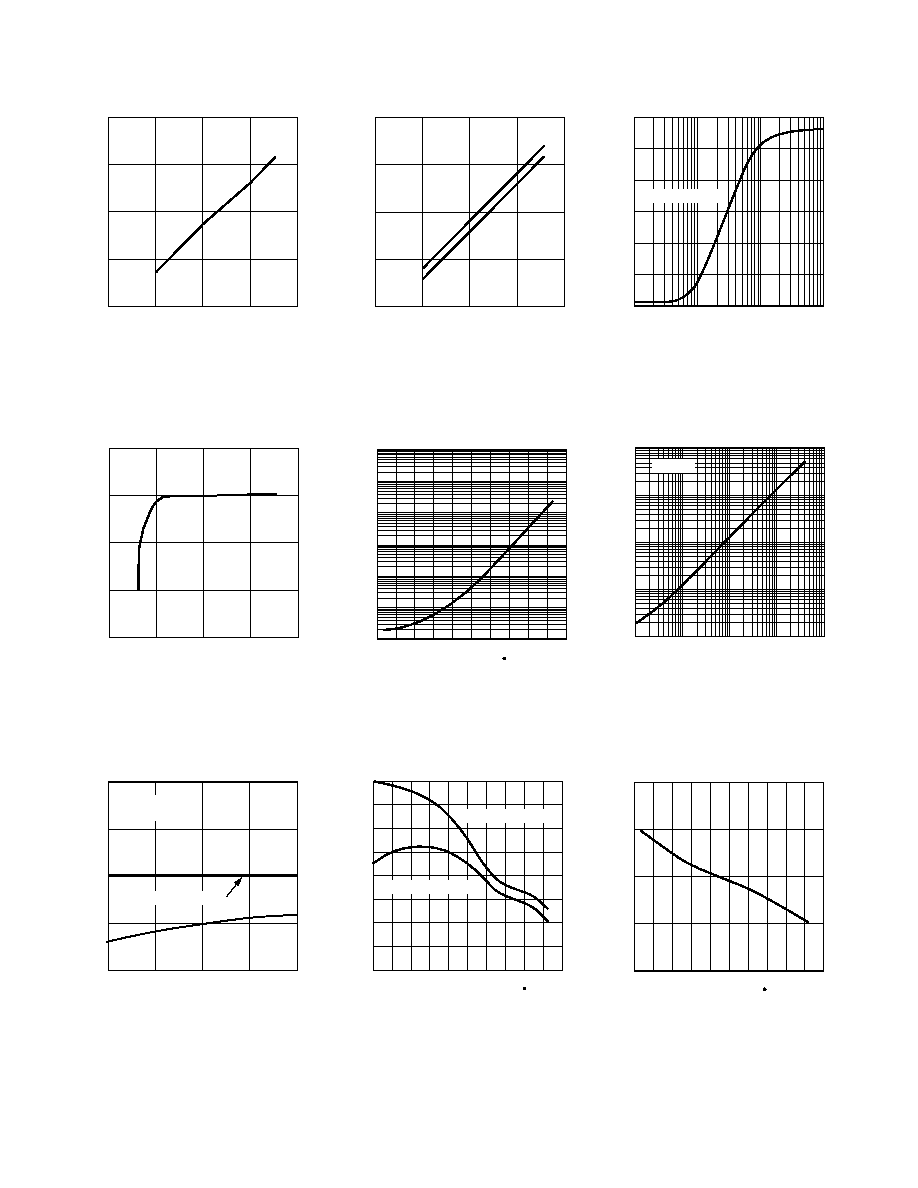
AD711Typical Performance Characteristics
4
SUPPLY VOLTAGE Volts
OUTPUT V
O
L
T
A
GE
SWING
V
o
lts
0
0
5
10
10
5
15
20
15
20
R
L
= 2k
25 C
+V
OUT
V
OUT
TPC 2. Output Voltage Swing vs.
Supply Voltage
TEMPERATURE C
INPUT BIAS CURRENT (V
CM
= 0)
Amps
10
12
60 40 20
0
20
40
60
80 100 120 140
10
11
10
10
10
9
10
8
10
7
10
6
TPC 5. Input Bias Current vs. Tem-
perature
AMBIENT TEMPERATURE C
SHORT
CIRCUIT CURRENT LIMIT
mA
60
10
40 20
0
20
40 60
80 100 120 140
12
14
16
18
20
22
24
26
OUTPUT CURRENT
+OUTPUT CURRENT
TPC 8. Short Circuit Current Limit
vs. Temperature
SUPPLY VOLTAGE Volts
INPUT V
O
L
T
A
GE
SWING
V
o
lts
0
0
5
10
10
5
15
20
15
20
R
L
= 2k
25 C
TPC 1. Input Voltage Swing vs.
Supply Voltage
SUPPLY VOLTAGE Volts
Q
UIESCENT CURRENT
mA
1.75
0
5
10
15
20
2.00
2.25
2.50
2.75
TPC 4. Quiescent Current vs. Sup-
ply Voltage
COMMON MODE VOLTAGE Volts
INPUT BIAS CURRENT
pA
0
10
50
25
75
100
MAX J GRADE LIMIT
5
0
5
10
V
S
= 15V
25 C
TPC 7. Input Bias Current vs. Com-
mon Mode Voltage
LOAD RESISTANCE
OUTPUT V
O
L
T
A
GE
SWING
V
o
lts
p-p
0
10
15
100
1k
10k
20
25
30
10
5
15V SUPPLIES
TPC 3. Output Voltage Swing vs.
Load Resistance
FREQUENCY Hz
OUTPUT IMPED
ANCE
0.01
1k
A
VCL
= 1
10k
100k
1M
10M
0.01
1
10
100
TPC 6. Output Impedance vs. Fre-
quency
TEMPERATURE C
UNITY GAIN BANDWIDTH
T
MHz
60
3.0
40 20
0
20
40 60
80 100 120 140
3.5
4.0
4.5
5.0
TPC 9. Unity Gain Bandwidth vs.
Temperature
REV. B
5
AD711
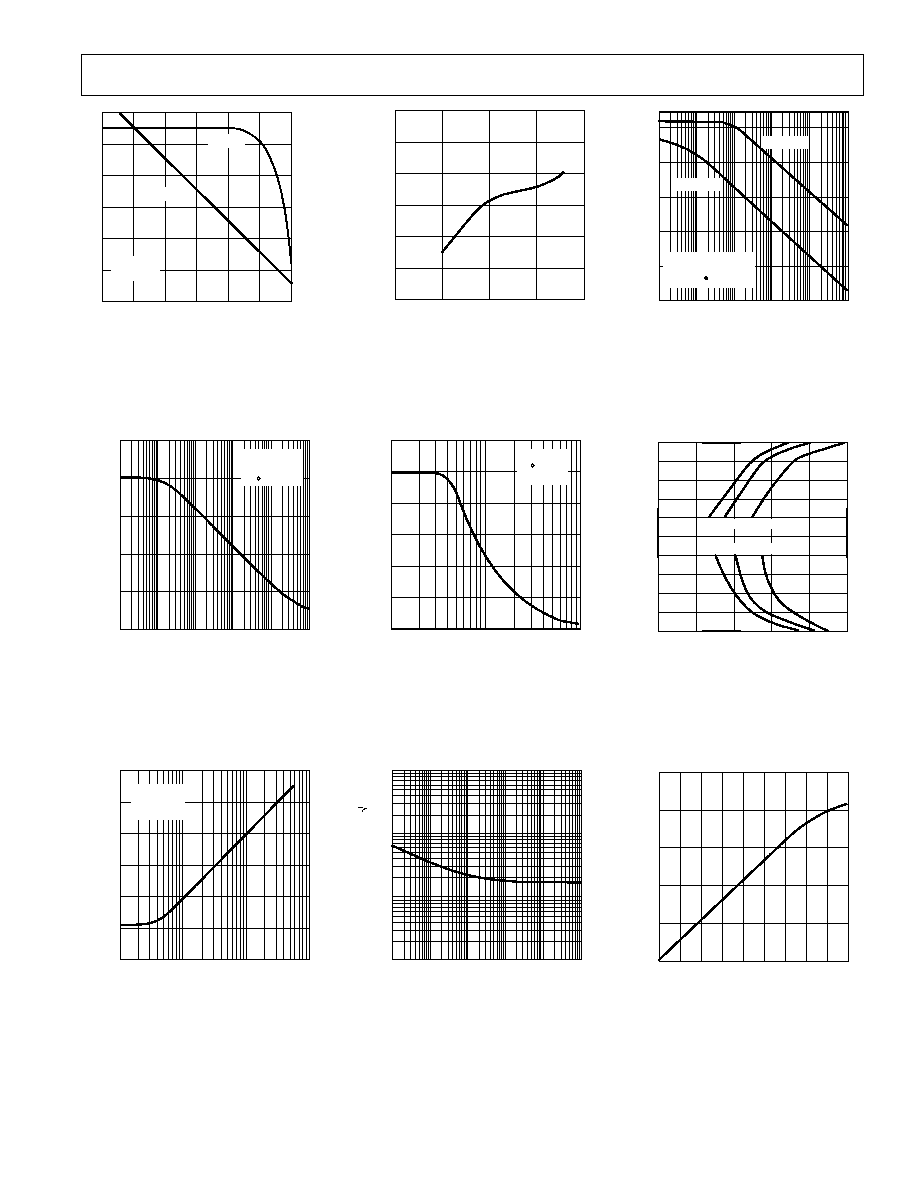
SUPPLY MODULATION FREQUENCY Hz
PO
WER SUPPL
Y REJECTION
dB
0
10
20
40
60
80
100
110
100
1k
10k
10k
1
SUPPLY
+SUPPLY
V
S
= 15 SUPPLIES
WITH 1V p-p SINE
WAVE 25 C
TPC 12. Power Supply Rejection
vs. Frequency
SETTLING TIME s
OUTPUT SWING FRIM 0V T
O
V
o
lts
0.5
10
8
6
4
2
0
2
2
4
6
8
0.6
0.7
0.8
0.9
1.0
ERROR
1% 0.1% 0.01%
1% 0.1% 0.01%
TPC 15. Output Swing and Error
vs. Settling Time
INPUT ERROR SIGNAL mV
(AT SUMMING JUNCTION)
SLEW RATE
V
s
0
0
100 200 300 400
5
10
15
20
25
500 600 700 800 900
TPC 18. Slew Rate vs. Input
Error Signal
SUPPLY VOLTAGE Volts
OPEN-LOOP GAIN
dB
0
95
5
10
15
20
100
105
110
115
120
125
R
L
= 2k
25 C
TPC 11. Open-Loop Gain vs.
Supply Voltage
INPUT FREQUENCY Hz
0
5
10
30
10M
100k
1M
15
20
25
OUTPUT V
O
L
T
A
GE
V
o
lts
p-p
R
L
= 2k
25 C
V
S
= 15V
TPC 14. Large Signal Frequency
Response
FREQUENCY Hz
1
1
10
10
INPUT NOISE
V
O
L
T
A
GE
nV/
Hz
100
1k
100
1k
10k
100k
TPC 17. Input Noise Voltage
Spectral Density
FREQUENCY Hz
OPEN LOOP GAIN
dB
10
20
100
1k
10k
100k
1M
0
20
40
60
10M
80
100
GAIN
R
L
= 2k
C = 100pF
PHASE
20
0
20
40
60
80
100
PHASE MARGIN
Degrees
TPC 10. Open-Loop Gain and
Phase Margin vs. Frequency
FREQUENCY Hz
CMR
dB
100
0
10
20
100
V
S
= 15V
V
CM
= 1V p-p
25 C
40
60
80
1k
10k
100k
1M
TPC 13. Common Mode Rejection
vs. Frequency
FREQUENCY Hz
THD
dB
130
100
120
110
100
90
80
70
1k
10k
100k
3V RMS
R
L
= 2k
C
L
= 100pF
TPC 16. Total Harmonic Distor-
tion vs. Frequency