 | –≠–ª–µ–∫—Ç—Ä–æ–Ω–Ω—ã–π –∫–æ–º–ø–æ–Ω–µ–Ω—Ç: AD712C | –°–∫–∞—á–∞—Ç—å:  PDF PDF  ZIP ZIP |
AD712 Data Sheet_D.p65
REV. D
Information furnished by Analog Devices is believed to be accurate and
reliable. However, no responsibility is assumed by Analog Devices for its
use, nor for any infringements of patents or other rights of third parties that
may result from its use. No license is granted by implication or otherwise
under any patent or patent rights of Analog Devices.
a
AD712
One Technology Way, P.O. Box 9106, Norwood, MA 02062-9106, U.S.A.
Tel: 781/329-4700
www.analog.com
Fax: 781/326-8703
© Analog Devices, Inc., 2002
Dual-Precision, Low-Cost,
High-Speed, BiFET Op Amp
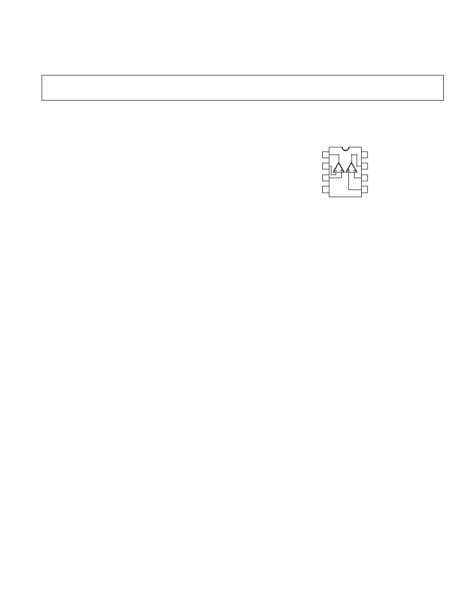
CONNECTION DIAGRAMS
Plastic Mini-DIP (N) Package
SOIC (R) Package and CERDIP (Q) Package
8
7
6
5
1
2
3
4
OUTPUT
INVERTING
OUTPUT
NONINVERTING
OUTPUT
V+
OUTPUT
INVERTING
INPUT
NONINVERTING
INPUT
V≠
AD712
AMPLIFIER NO. 2
AMPLIFIER NO. 1
FEATURES
Enhanced Replacement for LF412 and TL082
AC PERFORMANCE
Settles to 60.01% in 1.0 ms
16 V/ms Min Slew Rate (AD712J)
3 MHz Min Unity Gain Bandwidth (AD712J)
DC PERFORMANCE
0.30 mV Max Offset Voltage: (AD712C)
5 mV/8C Max Drift: (AD712C)
200 V/mV Min Open-Loop Gain (AD712K)
4 mV p-p Max Noise, 0.1 Hz to 10 Hz (AD712C)
Surface Mount Available in Tape and Reel in
Accordance with EIA-481A Standard
MIL-STD-883B Parts Available
Single Version Available: AD711
Quad Version: AD713
Available in Plastic Mini-DIP, Plastic SOIC, and
Hermetic CERDIP
PRODUCT DESCRIPTION
The AD712 is a high-speed, precision monolithic operational
amplifier offering high performance at very modest prices. Its
very low offset voltage and offset voltage drift are the results of
advanced laser wafer trimming technology. These performance
benefits allow the user to easily upgrade existing designs that use
older precision BiFETs and, in many cases, bipolar op amps.
The superior ac and dc performance of this op amp makes it
suitable for active filter applications. With a slew rate of 16 V/
µs
and a settling time of 1
µs to ± 0.01%, the AD712 is ideal as a
buffer for 12-bit D/A and A/D converters and as a high-speed
integrator. The settling time is unmatched by any similar IC
amplifier.
The combination of excellent noise performance and low input
current also make the AD712 useful for photo diode preamps.
Common-mode rejection of 88 dB and open loop gain of
400 V/mV ensure 12-bit performance even in high-speed unity
gain buffer circuits.
The AD712 is pinned out in a standard op amp configuration
and is available in seven performance grades. The AD712J and
AD712K are rated over the commercial temperature range of
0
∞C to 70∞C. The AD712A, AD712B, and AD712C are rated
over the industrial temperature range of ≠40
∞C to +85∞C. The
AD712S and AD712T are rated over the military temperature
range of ≠55
∞C to +125∞C and are available processed to MIL-
STD-883-B, Rev. C.
Extended reliability PLUS screening is available, specified over
the commercial and industrial temperature ranges. PLUS
screening includes 168-hour burn-in, as well as other environ-
mental and physical tests.
The AD712 is available in an 8-lead plastic mini-DIP, SOIC,
and CERDIP.
PRODUCT HIGHLIGHTS
1. The AD712 offers excellent overall performance at very
competitive prices.
2. Analog Devices' advanced processing technology and 100%
testing guarantee a low input offset voltage (0.3 mV max,
C grade, 3 mV max, J grade). Input offset voltage is specified
in the warmed-up condition. Analog Devices' laser wafer drift
trimming process reduces input offset voltage drifts to 5
µV/∞C
max on the AD712C.
3. Along with precision dc performance, the AD712 offers
excellent dynamic response. It settles to
±0.01% in 1 µs and
has a minimum slew rate of 16 V/
µs. Thus this device is ideal
for applications such as DAC and ADC buffers which require a
combination of superior ac and dc performance.
4. The AD712 has a guaranteed and tested maximum voltage
noise of 4
µV p-p, 0.1 Hz to 10 Hz (AD712C).
5. Analog Devices' well-matched, ion-implanted JFETs ensure
a guaranteed input bias current (at either input) of 50 pA
max (AD712C) and an input offset current of 10 pA max
(AD712C). Both input bias current and input offset current
are guaranteed in the warmed-up condition.
REV. D
≠2≠
AD712≠SPECIFICATIONS
(V
S
= 15 V @ T
A
= 25 C unless otherwise noted.)
AD712J/A/S
AD712K/B/T
AD712C
Parameter
Min
Typ
Max
Min
Typ
Max
Min
Typ
Max
Unit
INPUT OFFSET VOLTAGE
1
Initial Offset
0.3
3
/1/1
0.2
1.0
/0.7/0.7
0.1
0.3
mV
T
MIN
to T
MAX
4/2/2
2.0
/1.5/1.5
0.6
mV
vs. Temp
7
20/20/20
7
10
3
5
µV/∞C
vs. Supply
76
95
80
100
86
110
dB
T
MIN
to T
MAX
76/76/76
80
86
dB
Long-Term Offset Stability
15
15
15
µV/Month
INPUT BIAS CURRENT
2
V
CM
= 0 V
25
75
20
75
20
50
pA
V
CM
= 0 V @ T
MAX
0.6/1.6/26
1.7/4.8/77
0.5/1.3/20
1.7/4.8/77
1.3
3.2
nA
V
CM
=
±10 V
100
100
75
pA
INPUT OFFSET CURRENT
V
CM
= 0 V
10
25
5
25
5
10
pA
V
CM
= 0 V @ T
MAX
0.3/0.7/11
0.6/1.6/26
0.1/0.3/5
0.6/1.6/26
0.3
0.7
nA
MATCHING CHARACTERISTICS
Input Offset Voltage
3
/1/1
1.0
/0.7/0.7
0.3
mV
T
MIN
to T
MAX
4/2/2
2.0
/1.5/1.5
0.6
mV
Input Offset Voltage Drift
20/20/20
10
5
µV/∞C
Input Bias Current
25
25
10
pA
Crosstalk @ f = 1 kHz
120
120
120
dB
@ f = 100 kHz
90
90
90
dB
FREQUENCY RESPONSE
Small Signal Bandwidth
3.0
4.0
3.4
4.0
3.4
4.0
MHz
Full Power Response
200
200
200
kHz
Slew Rate
16
20
18
20
18
20
V/
µs
Settling Time to 0.01%
1.0
1.2
1.0
1.2
1.0
1.2
µs
Total Harmonic Distortion
0.0003
0.0003
0.0003
%
INPUT IMPEDANCE
Differential
3
◊ 10
12
5.5
3
◊ 10
12
5.5
3
◊ 10
12
5.5
pF
Common Mode
3
◊ 10
12
5.5
3
◊ 10
12
5.5
3
◊ 10
12
5.5
pF
INPUT VOLTAGE RANGE
Differential
3
±20
±20
±20
V
Common-Mode Voltage
4
+14.5, ≠11.5
+14.5, ≠11.5
+14.5, ≠11.5
T
MIN
to T
MAX
≠V
S
+ 4
+V
S
≠ 2
≠V
S
+ 4
+V
S
≠ 2
≠V
S
+ 4
+V
S
≠ 2
V
Common-Mode
Rejection Ratio
V
CM
=
±10 V
76
88
80
88
86
94
dB
T
MIN
to T
MAX
76/76/76
84
80
84
86
90
dB
V
CM
=
±11 V
70
84
76
84
76
90
dB
T
MIN
to T
MAX
70/70/70
80
74
80
74
84
dB
INPUT VOLTAGE NOISE
2
2
2
µV p-p
45
45
45
nV/
Hz
22
22
22
nV/
Hz
18
18
18
nV/
Hz
16
16
16
nV/
Hz
INPUT CURRENT NOISE
0.01
0.01
0.01
pA/
Hz
OPEN-LOOP GAIN
150
400
200
400
200
400
V/mV
100/100/100
100
100
V/mV
OUTPUT CHARACTERISTICS
Voltage
+13, ≠12.5
+13.9, ≠13.3
+13, ≠12.5
+13.9, ≠13.3
+13, ≠12.5
+13.9, ≠13.3
V
±12/±12/ 12 +13.8, ≠13.1
12
+13.8, ≠13.1
12
+13.8, ≠13.1
V
Current
25
25
25
mA
POWER SUPPLY
Rated Performance
±15
±15
±15
V
Operating Range
4.5
18
4.5
18
4.5
18
V
Quiescent Current
5.0
6.8
5.0
6.0
5.0
5.6
mA
NOTES
1
Input Offset Voltage specifications are guaranteed after 5 minutes of operation at T
A
= 25
∞C.
2
Bias Current specifications are guaranteed maximum at either input after 5 minutes of operation at T
A
= 25
∞C. For higher temperatures, the current doubles every 10∞C.
3
Defined as voltage between inputs, such that neither exceeds
±10 V from ground.
4
Typically exceeding ≠14.1 V negative common-mode voltage on either input results in an output phase reversal.
Specifications in boldface are tested on all production units at final electrical test. Results from those tests are used to calculate outgoing quality levels. All min and max
specifications are guaranteed, although only those shown in boldface are tested on all production units.
Specifications subject to change without notice.
REV. D
AD712
≠3≠
ABSOLUTE MAXIMUM RATINGS
1
Supply Voltage . . . . . . . . . . . . . . . . . . . . . . . . . . . . . . . .
±18 V
Internal Power Dissipation
2
Input Voltage
3
. . . . . . . . . . . . . . . . . . . . . . . . . . . . . . . .
±18 V
Output Short Circuit Duration . . . . . . . . . . . . . . . . . Indefinite
Differential Input Voltage . . . . . . . . . . . . . . . . . . +V
S
and ≠V
S
Storage Temperature Range (Q) . . . . . . . . . . ≠65
∞C to +150∞C
Storage Temperature Range (N, R) . . . . . . . . ≠65
∞C to +125∞C
Operating Temperature Range
AD712J/K . . . . . . . . . . . . . . . . . . . . . . . . . . . . . 0
∞C to 70∞C
AD712A/B/C . . . . . . . . . . . . . . . . . . . . . . . . ≠40
∞C to +85∞C
AD712S/T . . . . . . . . . . . . . . . . . . . . . . . . . ≠55
∞C to +125∞C
Lead Temperature Range (Soldering 60 sec) . . . . . . . . . 300
∞C
NOTES
1
Stresses above those listed under Absolute Maximum Ratings may cause perma-
nent damage to the device. This is a stress rating only; functional operation of the
device at these or any other conditions above those indicated in the operational
section of this specification is not implied. Exposure to absolute maximum rating
conditions for extended periods may affect device reliability.
2
Thermal Characteristics:
8-Lead Plastic Package:
JA
= 165
∞C/W
8-Lead Cerdip Package:
JC
= 22
∞C/W;
JA
= 110
∞C/W
8-Lead SOIC Package:
JA
= 100
∞C
3
For supply voltages less than
±18 V, the absolute maximum input voltage is equal
to the supply voltage.
ORDERING GUIDE
Temperature
Package
Package
Model
Range
Description
Option
AD712AQ
≠40
∞C to +85∞C
8-Lead Ceramic DIP
Q-8
AD712BQ
*
≠40
∞C to +85∞C
8-Lead Ceramic DIP
Q-8
AD712CN
*
≠40
∞C to +85∞C
8-Lead Plastic DIP
N-8
AD712JN
0
∞C to 70∞C
8-Lead Plastic DIP
N-8
AD712JR
0
∞C to 70∞C
8-Lead Plastic SOIC
R-8
AD712JR-REEL
0
∞C to 70∞C
8-Lead Plastic SOIC
R-8
AD712JR-REEL7
0
∞C to 70∞C
8-Lead Plastic SOIC
R-8
AD712KN
0
∞C to 70∞C
8-Lead Plastic DIP
N-8
AD712KR
0
∞C to 70∞C
8-Lead Plastic SOIC
R-8
AD712KR-REEL
0
∞C to 70∞C
8-Lead Plastic SOIC
R-8
AD712KR-REEL7
0
∞C to 70∞C
8-Lead Plastic SOIC
R-8
AD712SQ
*
≠55
∞C to +125∞C 8-Lead Ceramic DIP
Q-8
AD712SQ/883B
≠55
∞C to +125∞C 8-Lead Ceramic DIP
Q-8
AD712TQ
*
≠55
∞C to +125∞C 8-Lead Ceramic DIP
Q-8
AD712TQ/883B
*
≠55
∞C to +125∞C 8-Lead Ceramic DIP
Q-8
*
Not for new design, obsolete April 2002.
CAUTION
ESD (electrostatic discharge) sensitive device. Electrostatic charges as high as 4000 V readily
accumulate on the human body and test equipment and can discharge without detection. Although
the AD712 features proprietary ESD protection circuitry, permanent damage may occur on devices
subjected to high-energy electrostatic discharges. Therefore, proper ESD precautions are
recommended to avoid performance degradation or loss of functionality.
WARNING!
ESD SENSITIVE DEVICE
REV. D
AD712
≠4≠
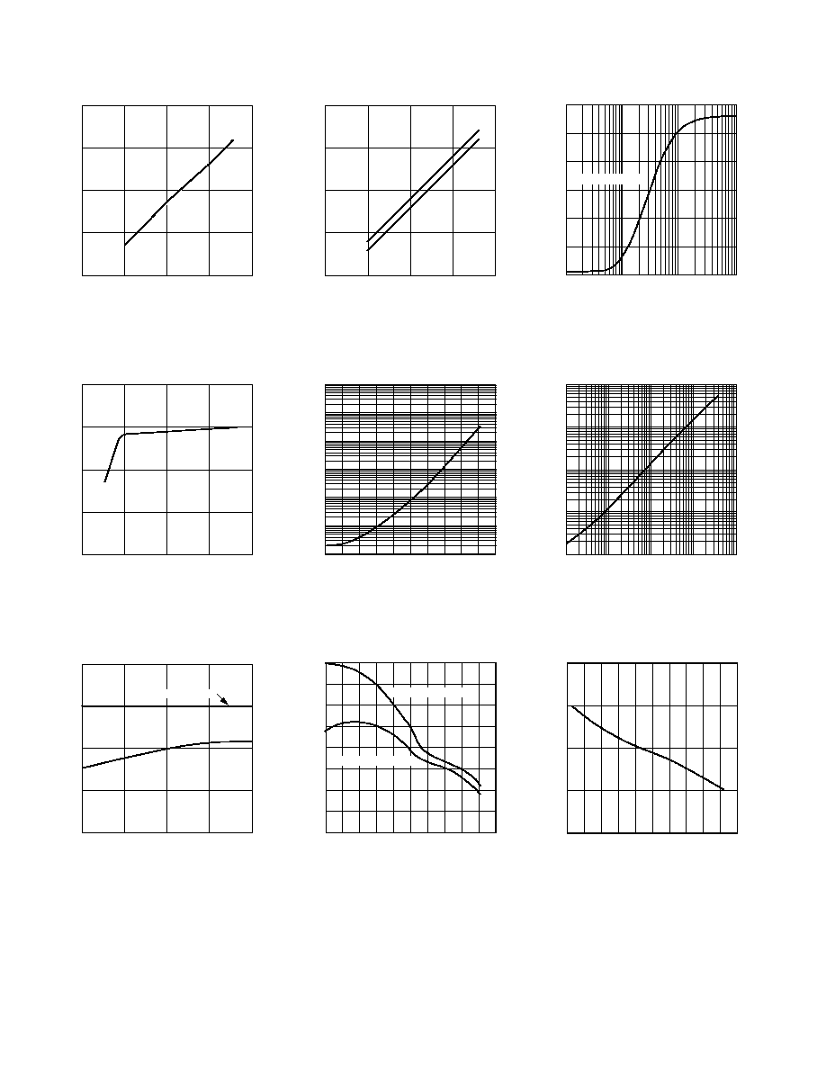
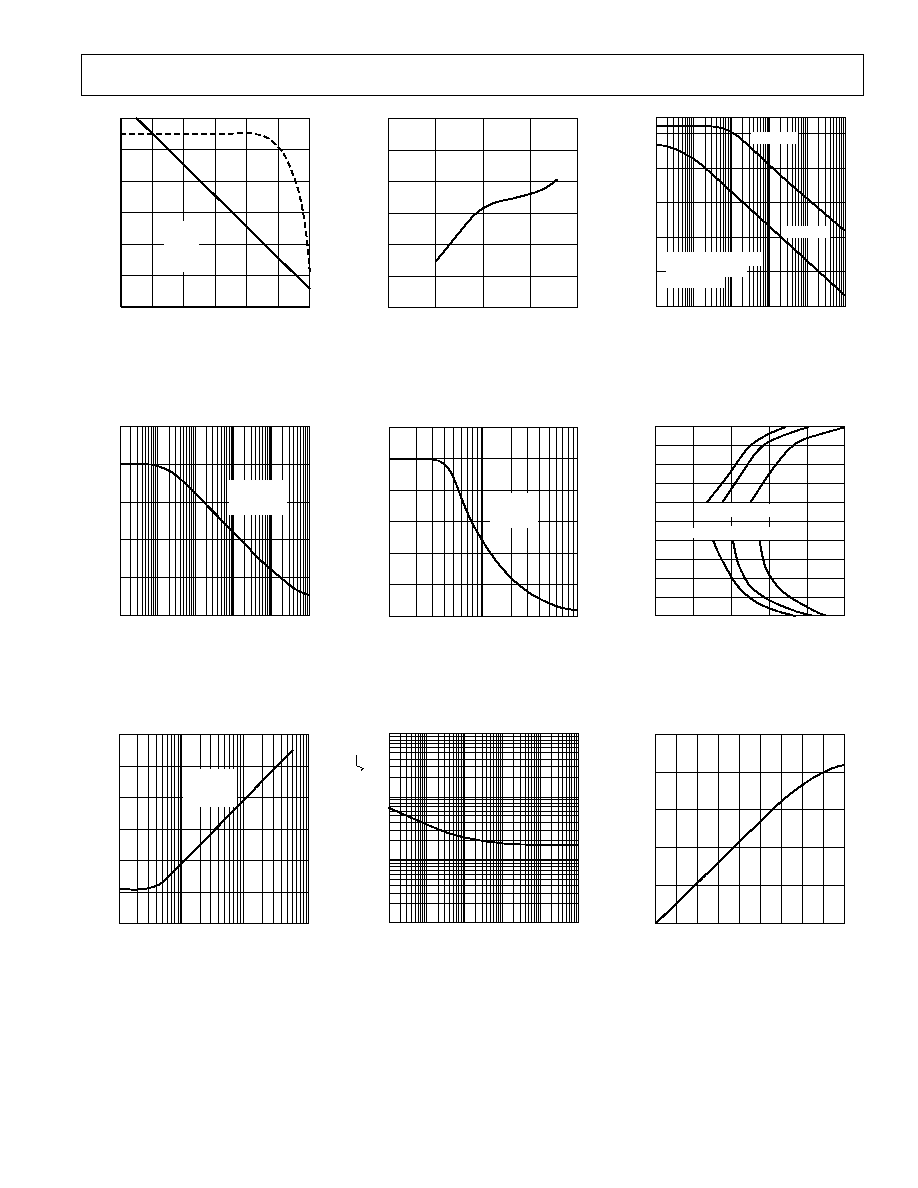
≠Typical Performance Characteristics
SUPPLY VOLTAGE V
INPUT VOLTAGE SWING
≠
V
20
15
0
0
5
20
10
15
10
5
R
L
= 2k
25 C
TPC 1. Input Voltage Swing vs.
Supply Voltage
SUPPLY VOLTAGE V
QUIESCENT CURRENT
≠
mA
6
5
2
0
5
20
10
15
4
3
TPC 4. Quiescent Current vs.
Supply Voltage
COMMON MODE VOLTAGE ≠ V
INPUT BIAS CURRENT
≠
pA
100
75
0
≠5
10
0
5
50
25
V
S
= 15V
25 C
≠10
MAX J GRADE LIMIT
TPC 7. Input Bias Current vs.
Common Mode Voltage
SUPPLY VOLTAGE V
OUTPUT VOLTAGE SWING
≠
V
20
15
0
0
5
20
10
15
10
5
R
L
= 2k
25 C
+V
OUT
≠V
OUT
TPC 2. Output Voltage Swing vs.
Supply Voltage
TEMPERATURE ≠ C
INPUT BIAS CURRENT (V
CM
= 0)
≠
Amps
10
12
≠60
0
140
≠40 ≠40
20
120
40
60
80 100
10
11
10
10
10
9
10
8
10
7
10
6
TPC 5. Input Bias Current vs.
Temperature
AMBIENT TEMPERATURE ≠ C
SHORT CIRCUIT CURRENT LIMIT
≠
mA
10
≠60
+ OUTPUT CURRENT
≠ OUTPUT CURRENT
≠40 ≠20
0
20
40 60
80 100 120 140
12
14
16
18
20
22
24
26
TPC 8. Short Circuit Current Limit
vs. Temperature
LOAD RESISTANCE ≠
OUTPUT VOLTAGE SWING
≠
V p
≠
p
30
25
0
10
100
10k
1k
15
10
5
20
15V SUPPLIES
TPC 3. Output Voltage Swing vs.
Load Resistance
FREQUENCY ≠ Hz
OUTPUT IMPEDANCE
≠
0.01
1k
1.0
0.1
10
100
10k
100k
1M
10M
TPC 6. Output Impedance vs.
Frequency
TEMPERATURE ≠ C
UNITY GAIN BANDWIDTH
≠
MHz
3.0
≠60 ≠40 ≠20
0
20
40 60
80 100 120 140
3.5
4.0
4.5
5.0
TPC 9. Unity Gain Bandwidth vs.
Temperature
REV. D
≠5≠
AD712
FREQUENCY ≠ Hz
OPEN LOOP GAIN
≠
dB
≠20
100
1k
1M
10
10k
100k
10M
0
20
40
60
80
100
GAIN
PHASE
2k
100pF
LOAD
≠20
0
20
40
60
80
100
PHASE MARGIN
≠
C
TPC 10. Open-Loop Gain and
Phase Margin vs. Frequency
FREQUENCY ≠ Hz
CMR
≠
dB
0
10
100
80
60
40
20
100
1k
10k
100k
1M
V
S
= 15V
V
CM
= 1Vp-p
25 C
TPC 13. Common Mode
Rejection vs. Frequency
FREQUENCY ≠ Hz
THD
≠
dB
≠70
100
10k
1k
≠80
≠90
≠100
≠110
≠120
≠130
100k
3V RMS
R
L
= 2k
C
L
= 100pF
TPC 16. Total Harmonic
Distortion vs. Frequency
SUPPLY VOLTAGE V
OPEN LOOP GAIN
≠
dB
125
0
5
20
10
15
R
L
= 2k
25 C
120
115
110
105
100
95
TPC 11. Open-Loop Gain vs. Sup-
ply Voltage
INPUT FREQUENCY ≠ Hz
OUTPUT VOLTAGE
≠
Volts p
≠
p
30
25
0
100k
10M
1M
15
10
5
20
R
L
= 2k
25 C
V
S
= 15V
TPC 14. Large Signal Frequency
Response
FREQUENCY ≠ Hz
INPUT NOISE VOLTAGE
≠
nV/
Hz
1k
1
10
100
10k
100k
100
10
1
1k
TPC 17. Input Noise Voltage
Spectral Density
SUPPLY MODULATION FREQUENCY ≠ Hz
POWER SUPPLY REJECTION
≠
dB
110
0
10
100
80
60
40
20
100
1k
10k
100k
1M
≠ SUPPLY
+ SUPPLY
V
S
= 15V SUPPLIES
WITH 1V p-p SINE
WAVE 25 C
TPC 12. Power Supply Rejection
vs. Frequency
SETTLING TIME ≠ s
OUTPUT SWING FROM 0V TO
VOLTS
≠8
0.5
≠6
≠4
≠2
0
4
6
8
10
2
≠10
0.6
0.7
0.8
0.9
1.0
0.01%
0.1%
1%
0.01%
0.1%
1%
ERROR
TPC 15. Output Swing and Error
vs. Settling Time
INPUT ERROR SIGNAL ≠ mV
(AT SUMMING JUNCTION)
SLEW RATE
≠
V/
s
5
100
10
15
20
25
200 300 400 500 600 700 800 900
0
0
TPC 18. Slew Rate vs. Input
Error Signal
REV. D
AD712
≠6≠
TEMPERATURE ≠ C
≠60
≠40
≠20
0
20
40
60
80
100
120
140
25
15
SLEW RATE
≠
V/
s
20
TPC 19. Slew Rate vs. Temperature
+V
S
OUTPUT
≠V
S
100pF
2k
0.1 F
INPUT
0.1 F
1/2
AD712
TPC 20. THD Test Circuit
1/2
AD712
CROSSTALK = 20 LOG
1/2
AD712
V
OUT
V
OUT
10V
IN
20k
2.2k
+V
S
20V p-p
5k
5k
V
IN
≠V
S
1
2
3
4
5
6
7
8
TPC 21. Crosstalk Test Circuit
+V
S
≠V
S
R
L
2k
0.1 F
0.1 F
1/2
AD712
C
L
100pF
V
IN
V
OUT
SQUARE
WAVE
INPUT
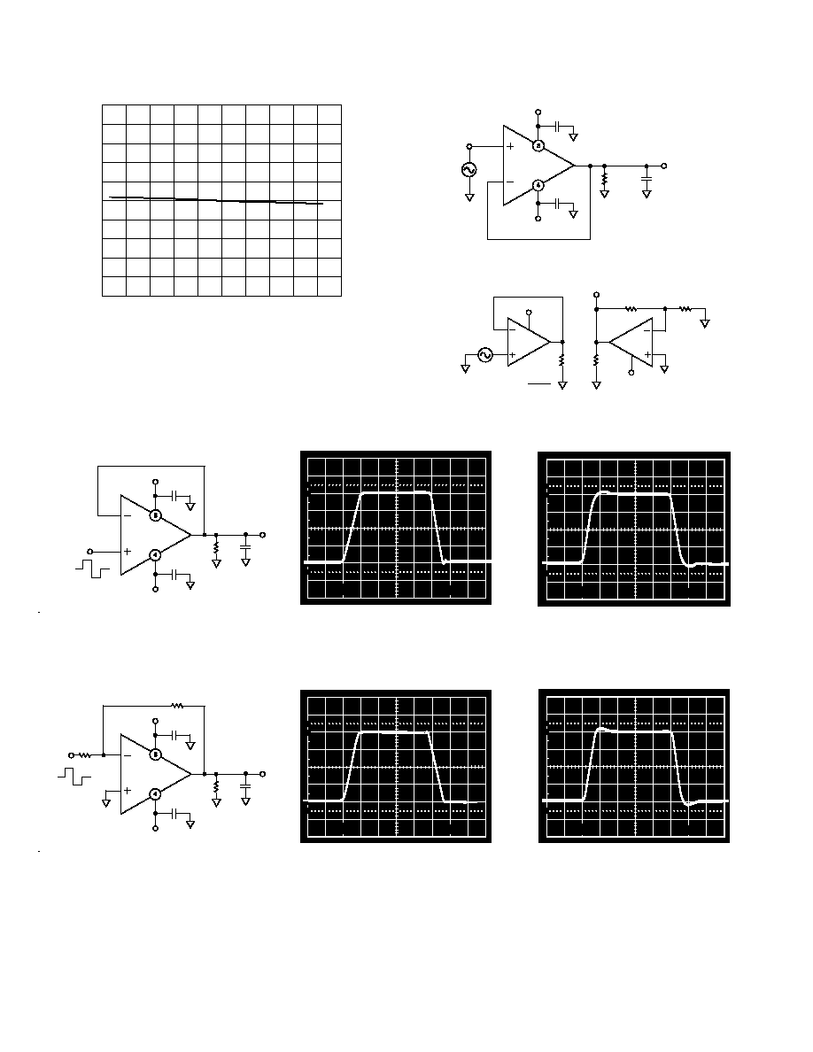
TPC 22a. Unity Gain Follower
+V
S
≠V
S
R
L
2k
0.1 F
0.1 F
1/2
AD712
C
L
100pF
V
IN
V
OUT
SQUARE
WAVE
INPUT
5k
5k
TPC 23a. Unity Gain Inverter
100
90
10
0%
1 s
5V
TPC 22b. Unity Gain Follower
Pulse Response (Large Signal)
100
90
10
0%
1 s
5V
TPC 23b. Unity Gain Inverter
Pulse Response (Large Signal)
100
10
0%
100ns
90
50mV
TPC 22c. Unity Gain Follower
Pulse Response (Small Signal)
100
10
0%
200ns
90
50mV
TPC 23c. Unity Gain Inverter Pulse
Response (Small Signal)
REV. D
AD712
≠7≠
OPTIMIZING SETTLING TIME
Most bipolar high-speed D/A converters have current outputs;
therefore, for most applications, an external op amp is required
for current-to-voltage conversion. The settling time of the con-
verter/op amp combination depends on the settling time of the
DAC and output amplifier. A good approximation is:
t
S
Total
= (t
S
DAC )
2
+ (t
S
AMP )
2
The settling time of an op amp DAC buffer will vary with the
noise gain of the circuit, the DAC output capacitance, and with
the amount of external compensation capacitance across the
DAC output scaling resistor.
Settling time for a bipolar DAC is typically 100 ns to 500 ns.
Previously, conventional op amps have required much longer
settling times than have typical state-of-the-art DACs; therefore,
the amplifier settling time has been the major limitation to a
high-speed voltage-output D-to-A function. The introduction of
the AD711/AD712 family of op amps with their 1
µs (to ±0.01%
of final value) settling time now permits the full high-speed
capabilities of most modern DACs to be realized.
In addition to a significant improvement in settling time, the
low offset voltage, low offset voltage drift, and high open-loop
gain of the AD711/AD712 family assure 12-bit accuracy over
the full operating temperature range.
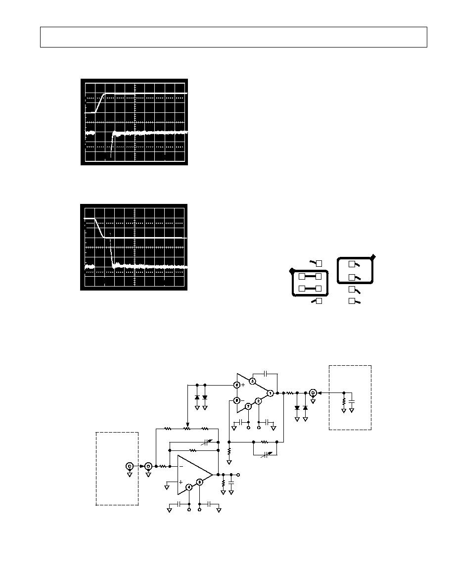
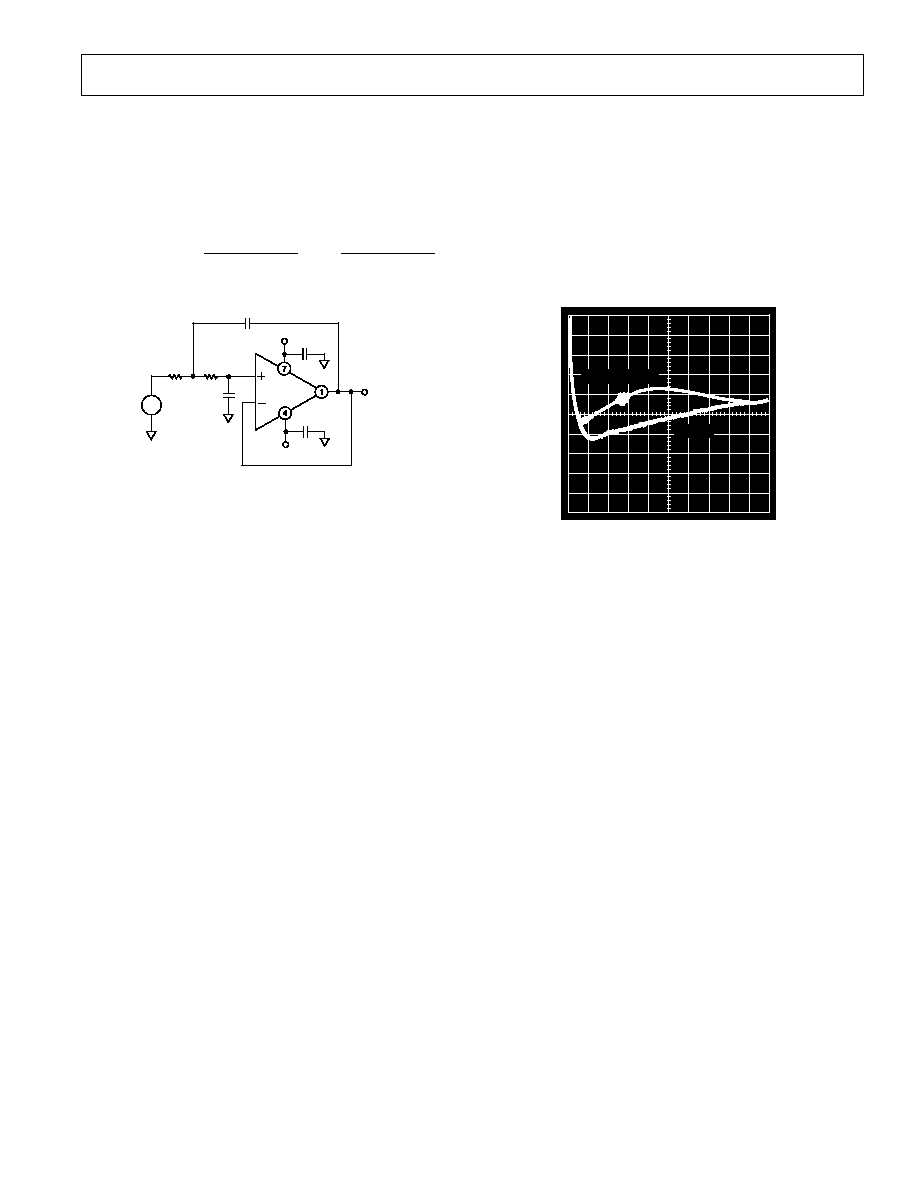
The excellent high-speed performance of the AD712 is shown in
the oscilloscope photos of Figure 2. Measurements were taken
using a low input capacitance amplifier connected directly to the
summing junction of the AD712 ≠ both photos show the worst
case situation: a full-scale input transition. The DAC's 4 k
[10 k
||8 k = 4.4 k] output impedance together with a
10 k
feedback resistor produce an op amp noise gain of 3.25.
The current output from the DAC produces a 10 V step at the
op amp output (0 to ≠10 V Figure 2a, ≠10 V to 0 V Figure 2b.)
Therefore, with an ideal op amp, settling to
±1/2 LSB (±0.01%)
requires that 375
µV or less appears at the summing junction.
This means that the error between the input and output (that
voltage which appears at the AD712 summing junction) must be
less than 375
µV. As shown in Figure 2, the total settling time
for the AD712/AD565 combination is 1.2 microseconds.
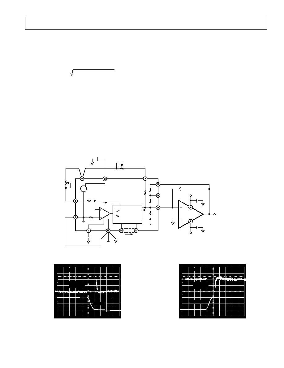
+15V
0.1 F
0.1 F
1/2
AD712
10pF
OUTPUT
≠10V TO +10V
AD565A
DAC
≠15V
I
OUT
= 4
I
REF
CODE
I
REF
BIPOLAR
OFFSET ADJUST
I
O
0.1 F
R1
100
R2
100
GAIN
ADJUST
REF
IN
REF
GND
20k
≠V
EE
0.1 F
POWER
GND
MSB
LSB
8k
5k
5k
10V
19.95k
0.5mA
DAC
OUT
10V
SPAN
20V
SPAN
V
CC
REF
OUT
BIPOLAR
OFF
9.95k
+
≠
Figure 1.
±10 V Voltage Output Bipolar DAC
100
10
0%
500ns
90
0V
≠10V
OUTPUT
5V
1mV
SUMMING
JUNCTION
a. (Full-Scale Negative Transition)
100
10
0%
500ns
90
0V
≠10V
SUMMING
JUNCTION
OUTPUT
5V
1mV
b. (Full-Scale Positive Transition)
Figure 2. Settling Characteristics for AD712 with AD565A
REV. D
AD712
≠8≠
When R
O
and I
O
are replaced with their Thevenin V
IN
and R
IN
equivalents, the general purpose inverting amplifier of Figure 3b
is created. Note that when using this general model, capacitance
C
X
is
either the input capacitance of the op amp if a simple in-
verting op amp is being simulated
or the combined capacitance of
the DAC output and the op amp input if the DAC buffer is being
modeled.
1/2
AD712
V
OUT
R
L
C
L
C
F
R
V
IN
R
IN
C
X
Figure 3b. Simplified Model of the AD712
Used as an Inverter
In either case, the capacitance C
X
causes the system to go from
a one-pole to a two-pole response; this additional pole increases
settling time by introducing peaking or ringing in the op amp
output. Since the value of C
X
can be estimated with reasonable
accuracy, Equation 2 can be used to choose a small capacitor,
C
F
, to cancel the input pole and optimize amplifier response.
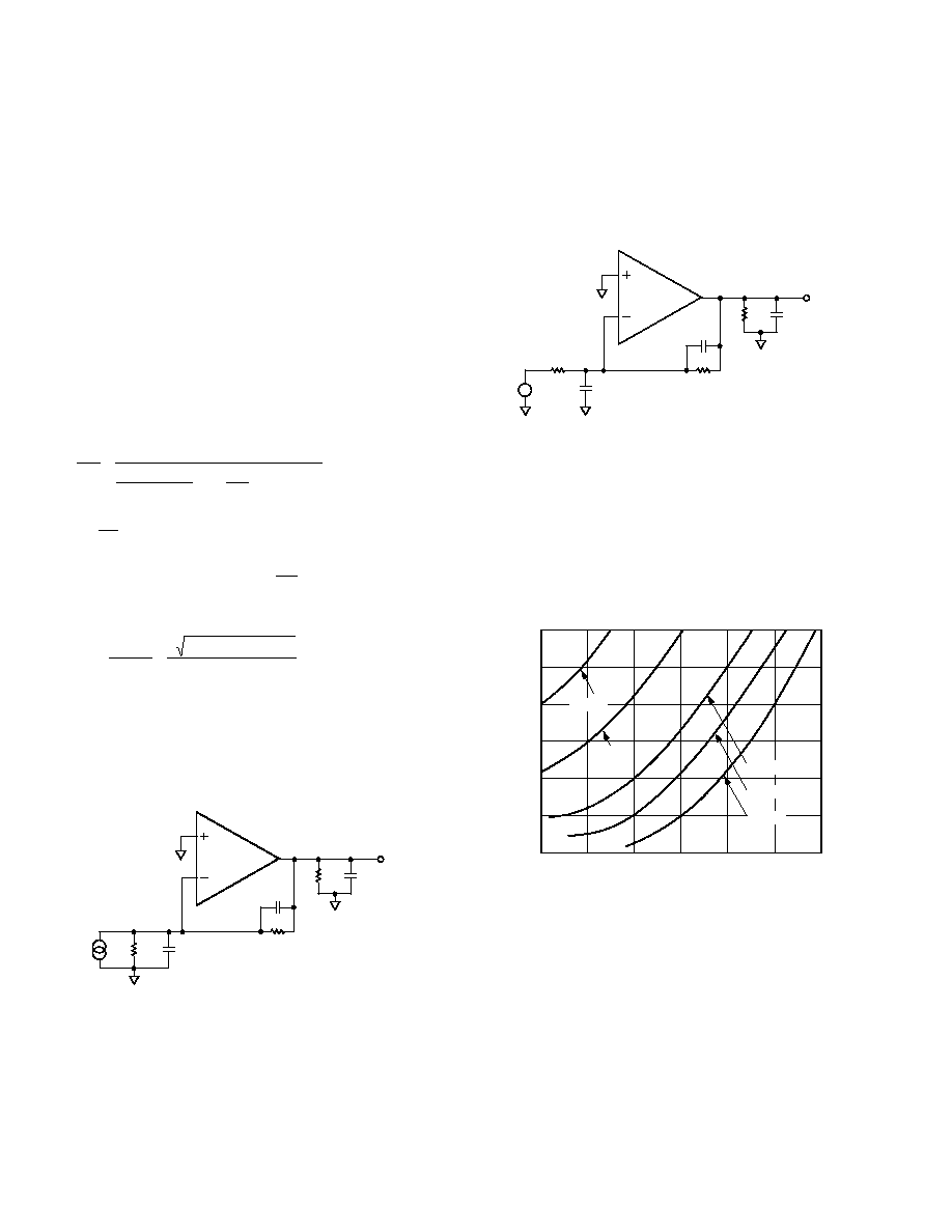
Figure 4 is a graphical solution of Equation 2 for the AD712
with R = 4 k
.
C
F
C
X
40
30
0
10
0
20
10
G
N
= 3.0
G
N
= 2.0
G
N
= 1.5
G
N
= 1.0
20
30
40
50
60
50
60
G
N
= 4.0
Figure 4. Value of Capacitor C
F
vs. Value of C
X
OP AMP SETTLING TIME -
A MATHEMATICAL MODEL
The design of the AD712 gives careful attention to optimizing
individual circuit components; in addition, a careful trade-off
was made: the gain bandwidth product (4 MHz) and slew rate
(20 V/
µs) were chosen to be high enough to provide very fast
settling time but not too high to cause a significant reduction in
phase margin (and therefore, stability). Thus designed, the
AD712 settles to
± 0.01%, with a 10 V output step, in under
1
µs, while retaining the ability to drive a 250 pF load capacitance
when operating as a unity gain follower.
If an op amp is modeled as an ideal integrator with a unity gain
crossover frequency of
/2
, Equation 1 will accurately describe
the small signal behavior of the circuit of Figure 3a, consisting
of an op amp connected as an I-to-V converter at the output of
a bipolar or CMOS DAC. This equation would completely
describe the output of the system if not for the op amp's finite
slew rate and other nonlinear effects.
V
O
I
IN
=
≠
R
R(C
f
= C
X
)
s
2
+
G
N
+ RC
f
s +1
(1)
where
2
= op amp's unity gain frequency
G
N
= "noise" gain of circuit
1
+ R
R
O
This equation may then be solved for C
f
:
C
f
=
2
- G
N
R
+
2
RC
X
+ (1- G
N
)
R
(2)
In these equations, capacitor C
X
is the total capacitor appearing
the inverting terminal of the op amp. When modeling a DAC
buffer application, the Norton equivalent circuit of Figure 3a
can be used directly; capacitance C
X
is the total capacitance of
the output of the DAC plus the input capacitance of the op amp
(since the two are in parallel).
1/2
AD712
V
OUT
R
L
C
L
C
F
R
I
O
R
O
C
X
Figure 3a. Simplified Model of the AD712 Used as a
Current-Out DAC Buffer
REV. D
AD712
≠9≠
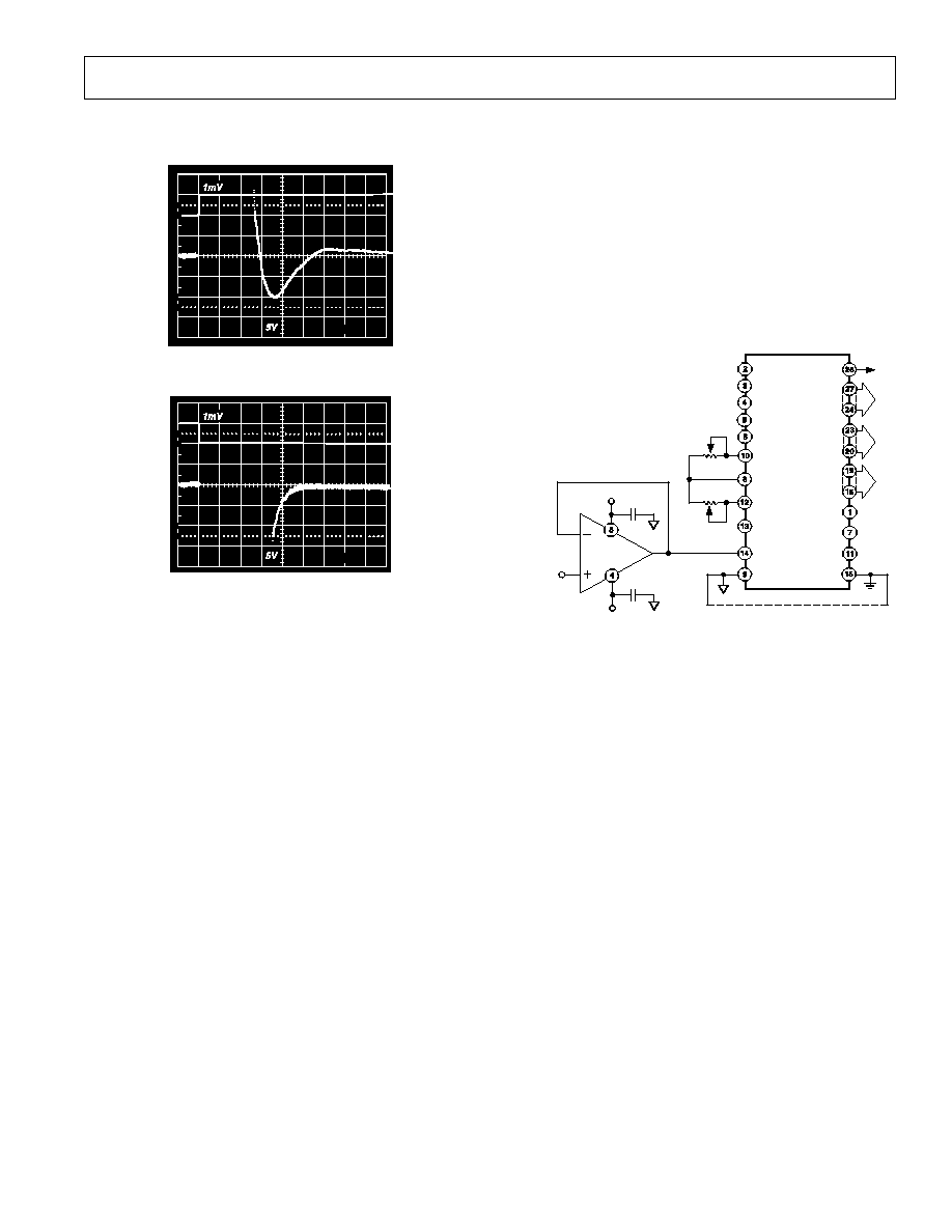
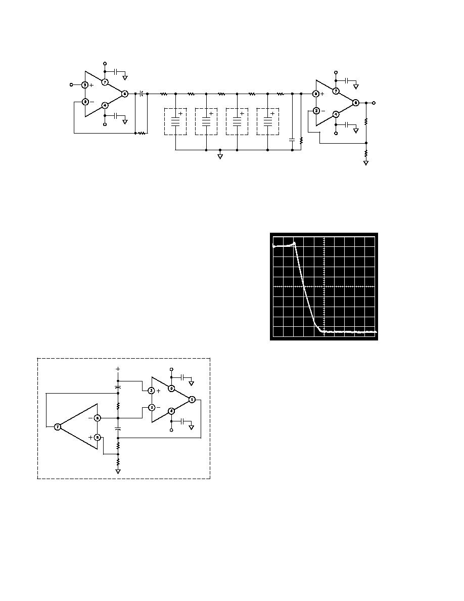
The photos of Figures 5a and 5b show the dynamic response of
the AD712 in the settling test circuit of Figure 6.
100
10
0%
500ns
90
5mV
5V
Figure 5a. Settling Characteristics 0 V to +10 V Step
Upper Trace: Output of AD712 Under Test (5 V/Div)
Lower Trace: Amplified Error Voltage (0.01%/Div)
100
10
0%
500ns
90
5mV
5V
Figure 5b. Settling Characteristics 0 V to ≠10 V Step
Upper Trace: Output of AD712 Under Test (5 V/Div)
Lower Trace: Amplified Error Voltage (0.01%/Div)
+15V
0.1 F
1/2
AD712
10pF
≠15V
5k
4.99k
0.47 F
1/2
AD712
0.47 F
200
4.99k
5-18pF
0.1 F
10k
10k
V
IN
V
ERROR
5
HP2835
HP2835
20pF
1M
10k
0.2-0.6pF
1.1k
5pF
TEKTRONIX 7A26
OSCILLOSCOPE
PREAMP
INPUT SECTION
DATA
DYNAMICS
5109
(OR EQUIVALENT
FLAT TOP
PULSE
GENERATION)
205
≠15V +15V
V
OUT
Figure 6. Settling Time Test Circuit
The input of the settling time fixture is driven by a flat-top pulse
generator. The error signal output from the false summing node
of A1 is clamped, amplified by A2 and then clamped again. The
error signal is thus clamped twice: once to prevent overloading
amplifier A2 and then a second time to avoid overloading the
oscilloscope preamp. The Tektronix oscilloscope preamp type
7A26 was carefully chosen because it does not overload with
these input levels. Amplifier A2 needs to be a very high speed
FET-input op amp; it provides a gain of 10, amplifying the error
signal output of A1.
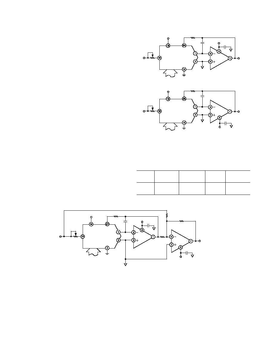
GUARDING
The low input bias current (15 pA) and low noise characteristics
of the AD712 BiFET op amp make it suitable for electrometer
applications such as photo diode preamplifiers and picoampere
current-to-voltage converters. The use of a guarding technique,
such as that shown in Figure 7, in printed circuit board layout
and construction is critical to minimize leakage currents. The
guard ring is connected to a low impedance potential at the same
level as the inputs. High impedance signal lines should not be
extended for any unnecessary length on the printed circuit board.
8
7
6
5
4
3
2
1
PLASTIC MINI-DIP (N) PACKAGE
CERDIP (Q) PACKAGE
AND SOIC (R) PACKAGE
Figure 7. Board Layout for Guarding Inputs
REV. D
AD712
≠10≠
D/A CONVERTER APPLICATIONS
The AD712 is an excellent output amplifier for CMOS DACs.
It can be used to perform both 2-quadrant and 4-quadrant opera-
tion. The output impedance of a DAC using an inverted R-2R
ladder approaches R for codes containing many 1s, 3R for codes
containing a single 1, and for codes containing all zero, the output
impedance is infinite.
For example, the output resistance of the AD7545 will modulate
between 11 k
and 33 k. Therefore, with the DAC's internal
feedback resistance of 11 k
, the noise gain will vary from 2 to
4/3. This changing noise gain modulates the effect of the input
offset voltage of the amplifier, resulting in nonlinear DAC amplifier
performance.
The AD712K with guaranteed 700
µV offset voltage minimizes
this effect to achieve 12-bit performance.
Figures 8 and 9 show the AD712 and AD7545 (12-bit CMOS
DAC) configured for unipolar binary (2-quadrant multiplication)
or bipolar (4-quadrant multiplication) operation. Capacitor C1
provides phase compensation to reduce overshoot and ringing.
+15V
1/2
AD712
GAIN
ADJUST
V
IN
V
REF
V
DD
R
FB
OUT1
AGND
AD7545
DGND
V
OUTA
R2A*
*REFER TO
TABLE I
DB11≠DB0
ANALOG
COMMON
C1A
33pF
0.1 F
V
DD
R1A*
1/2
AD712
GAIN
ADJUST
V
IN
V
REF
V
DD
R
FB
OUT1
AGND
AD7545
DGND
V
OUTB
R2B*
*REFER TO
TABLE I
DB11≠DB0
ANALOG
COMMON
C1B
33pF
0.1 F
≠15V
R1B*
V
DD
Figure 8. Unipolar Binary Operation
R1 and R2 calibrate the zero offset and gain error of the DAC.
Specific values for these resistors depend upon the grade of
AD7545 and are shown below.
Table I. Recommended Trim Resistor Values vs. Grades
of the AD7545 for V
DD
= 5 V
Trim
Resistor
JN/AQ/SD
KN/BQ/TD
LN/UD
GLN/GUD
R1
500
200
100
20
R2
150
68
33
6.8
+15V
1/2
AD712
GAIN
ADJUST
V
IN
V
REF
V
DD
R
FB
OUT1
AGND
AD7545
DGND
R2*
*FOR VALUES OF
R1 AND R2 SEE TABLE I
DATA INPUT
ANALOG
COMMON
C1
33pF
0.1 F
V
DD
R1*
1/2
AD712
V
OUT
0.1 F
≠15V
R3
10k
1%
R5
20k
1%
R4
20k
1%
12
DB11≠DB0
Figure 9. Bipolar Operation
REV. D
AD712
≠11≠
Figures 10a and 10b show the settling time characteristics of the
AD712 when used as a DAC output buffer for the AD7545.
100
10
0%
500ns
90
a. Full-Scale Positive Transition
100
10
0%
500ns
90
b. Full-Scale Negative Transition
Figure 10. Settling Characteristics for AD712 with AD7545
NOISE CHARACTERISTICS
The random nature of noise, particularly in the 1/f region, makes it
difficult to specify in practical terms. At the same time, designers of
precision instrumentation require certain guaranteed maximum
noise levels to realize the full accuracy of their equipment.
The AD712C grade is specified at a maximum level of 4.0
µV p-p,
in a 0.1 Hz to 10 Hz bandwidth. Each AD712C receives a 100%
noise test for two 10-second intervals; devices with any excursion
in excess of 4.0
µV are rejected. The screened lot is then submitted
to Quality Control for verification on an AQL basis.
All other grades of the AD712 are sample-tested on an AQL basis
to a limit of 6
µV p-p, 0.1 Hz to 10 Hz.
DRIVING THE ANALOG INPUT OF AN A/D CONVERTER
An op amp driving the analog input of an A/D converter, such as
that shown in Figure 11, must be capable of maintaining a con-
stant output voltage under dynamically changing load conditions.
In successive approximation converters, the input current is
compared to a series of switched trial currents. The comparison
point is diode clamped but may deviate several hundred milli-
volts resulting in high frequency modulation of A/D input current.
The output impedance of a feedback amplifier is made artifi-
cially low by the loop gain. At high frequencies, where the loop
gain is low, the amplifier output impedance can approach its
open loop value. Most IC amplifiers exhibit a minimum open
loop output impedance of 25
due to current limiting resistors.
+15V
1/2
AD712
0.1 F
0.1 F
≠15V
10V
ANALOG
INPUT
GAIN
ADJUST
ANALOG COM
R2
100
OFFSET
ADJUST
AD574
12/8
R1
100
CS
A
O
R/C
CE
REF IN
REF OUT
BIP OFF
10V
IN
ANA
COM
20V
IN
STS
HIGH
BITS
+5V
DIG
COM
+15V
≠15V
MIDDLE
BITS
LOW
BITS
Figure 11. AD712 as ADC Unity Gain Buffer
A few hundred microamps reflected from the change in converter
loading can introduce errors in instantaneous input voltage. If
the A/D conversion speed is not excessive and the bandwidth of
the amplifier is sufficient, the amplifier's output will return to
the nominal value before the converter makes its comparison.
However, many amplifiers have relatively narrow bandwidth
yielding slow recovery from output transients. The AD712 is
ideally suited to drive high speed A/D converters since it offers
both wide bandwidth and high open-loop gain.
REV. D
AD712
≠12≠
100
10
0%
90
200ns
500mV
PD711 BUFF
≠10V ADC IN
a. Source Current = 2 mA
100
10
0%
200ns
90
500mV
PD711 BUFF
≠5V ADC IN
b. Sink Current = 1 mA
Figure 12. ADC Input Unity Gain Buffer Recovery Times
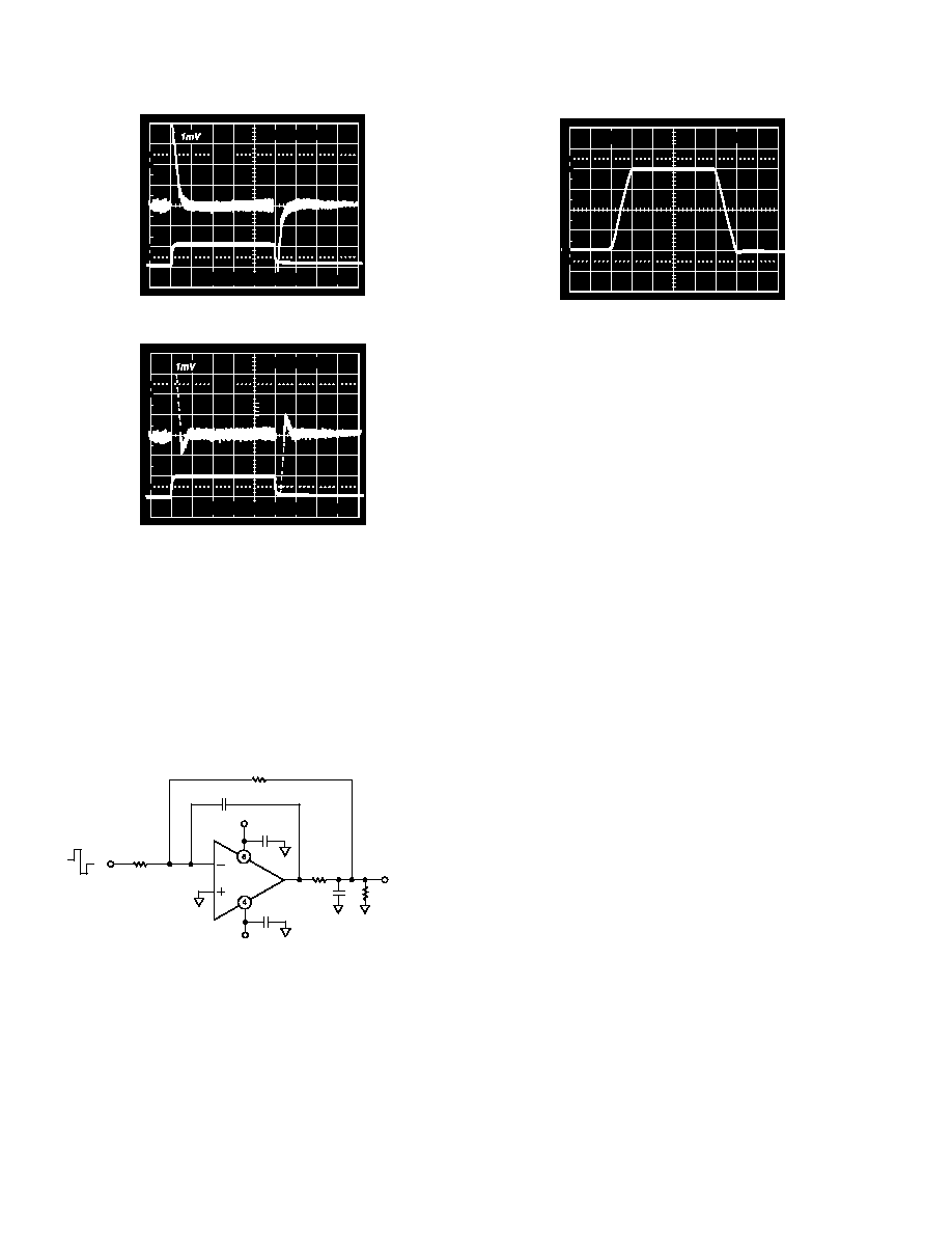
DRIVING A LARGE CAPACITIVE LOAD
The circuit in Figure 13 employs a 100
isolation resistor which
enables the amplifier to drive capacitive loads exceeding 1500 pF;
the resistor effectively isolates the high frequency feedback from
the load and stabilizes the circuit. Low frequency feedback is
returned to the amplifier summing junction via the low pass
filter formed by the 100
series resistor and the load capaci-
tance, C
L
. Figure 14 shows a typical transient response for this
connection.
1/2
AD712
0.1 F
0.1 F
≠V
IN
+V
IN
INPUT
TYPICAL CAPACITANCE
LIMIT FOR VARIOUS
LOAD RESISTORS
R
1
C
1
UP TO
2k
1500pF
10k
1500pF
20
1000pF
C
1
R
1
4.99k
4.99k
30pF
OUTPUT
100
+
≠
≠
+
Figure 13. Circuit for Driving a Large Capacitive Load
100
90
10
0%
1 s
5V
Figure 14. Transient Response R
L
= 2 k
, C
L
= 500 pF
ACTIVE FILTER APPLICATIONS
In active filter applications using op amps, the dc accuracy of
the amplifier is critical to optimal filter performance. The
amplifier's offset voltage and bias current contribute to output
error. Offset voltage will be passed by the filter and may be
amplified to produce excessive output offset. For low frequency
applications requiring large value input resistors, bias currents
flowing through these resistors will also generate an offset voltage.
In addition, at higher frequencies, an op amp's dynamics must
be carefully considered. Here, slew rate, bandwidth, and open-
loop gain play a major role in op amp selection. The slew rate
must be fast as well as symmetrical to minimize distortion. The
amplifier's bandwidth in conjunction with the filter's gain will
dictate the frequency response of the filter.
The use of a high performance amplifier such as the AD712 will
minimize both dc and ac errors in all active filter applications.
REV. D
AD712
≠13≠
SECOND ORDER LOW PASS FILTER
Figure 15 depicts the AD712 configured as a second order
Butterworth low pass filter. With the values as shown, the corner
frequency will be 20 kHz; however, the wide bandwidth of the
AD712 permits a corner frequency as high as several hundred
kilohertz. Equations for component selection are shown below.
R1 = R2 = user selected (typical values: 10 k
≠ 100 k)
C1 (in farads )
=
1.414
(2
)( f
cutoff
)(
R1)
C2
=
0.707
(2
)( f
cutoff
)(
R1)
+15V
1/2
AD712
0.1 F
0.1 F
≠15V
V
OUT
C2
280pF
R2
20k
R1
20k
C1
560pF
V
IN
Figure 15. Second Order Low-Pass Filter
An important property of filters is their out-of-band rejection.
The simple 20 kHz low pass filter shown in Figure 15, might be
used to condition a signal contaminated with clock pulses or
sampling glitches which have considerable energy content at
high frequencies.
The low output impedance and high bandwidth of the AD712
minimize high frequency feedthrough as shown in Figure 16.
The upper trace is that of another low-cost BiFET op amp show-
ing 17 dB more feedthrough at 5 MHz.
REF 20.0 dBm
10 dB/DIV
RANGE 15.0 dBm
OFFSET .0 Hz
0 dB
CENTER 5 000 000.0 Hz
RBW 30 kHz
SPAN 10 000 000.0 Hz
ST .8 SEC
VBW 30 kHz
AD712
TYPICAL BIFET
Figure 16. TBD
REV. D
AD712
≠14≠
+15V
0.001 F
100k
0.1 F
0.1 F
A2
AD711
≠15V
+15V
0.1 F
0.1 F
A1
AD711
≠15V
*
D
*
C
*
B
*
A
2800
6190
6490
6190
2800
V
IN
0.001 F
124k
4.99k
4.99k
V
OUT
4.9395E
≠15
5.9276E
≠15
5.9276E
≠15
4.9395E
≠15
*
SEE TEXT
Figure 17. 9-Pole Chebychev Filter
9-POLE CHEBYCHEV FILTER
Figure 17 shows the AD712 and its dual counterpart, the AD711,
as a 9-pole Chebychev filter using active frequency dependent
negative resistors (FDNR). With a cutoff frequency of 50 kHz
and better than 90 dB rejection, it may be used as an antialiasing
filter for a 12-bit data acquisition system with 100 kHz throughput.
As shown in Figure 17, the filter is comprised of four FDNRs (A,
B, C, D) having values of 4.9395 10
≠15
and 5.9276 10
≠15
farad-seconds. Each FDNR active network provides a two-pole
response for a total of 8 poles. The 9th pole consists of a 0.001
µF
capacitor and a 124 k
resistor at Pin 3 of amplifier A2. Figure 18
depicts the circuits for each FDNR with the proper selection of
R. To achieve optimal performance, the 0.001
µF capacitors
must be selected for 1% or better matching and all resistors
should have 1% or better tolerance.
+15V
0.001 F
4.99k
0.1 F
0.1 F
1/2
AD712
≠15V
1.0k
R:
24.9k
FOR 4.9395E
≠15
29.4k
FOR 5.9276E
≠15
1/2
AD712
0.001 F
R
Figure 18. FDNR for 9-Pole Chebychev Filter
REF 5.0 dBm
10 dB/DIV
RANGE ≠5.0 dBm
MARKER 96 800.0 Hz
≠90 dBm
START.0 Hz
RBW 300 Hz
STOP 200 000.0 Hz
ST 69.6 SEC
VBW 30 Hz
Figure 19. High Frequency Response for 9-Pole
Chebychev Filter
REV. D
AD712
≠15≠
OUTLINE DIMENSIONS
Dimensions shown in inches and (mm).
Mini-DIP
(N-8)
8
1
4
5
0.390 (9.91)
0.250
(6.35)
PIN 1
SEATING
PLANE
0.018 0.003
(0.460 0.081)
0.035 0.01
(0.890 0.25)
0.165 0.01
4.19 0.25
0.18 0.01
(4.57 0.76)
0.033 (0.84)
NOM
0.100
(2.54)
TYP
0.125 (3.18)
MIN
0.300 (7.62)
REF
0.011 0.003
(0.204 0.081)
0.195 (4.95)
0.115 (2.93)
0.310
(7.87)
15
0
CERDIP
(Q-8)
8
1
4
5
0.310 (7.87)
0.220 (5.59)
PIN 1
0.005 (0.13)
MIN
0.055 (1.35)
MAX
SEATING
PLANE
0.014 (0.36)
0.023 (0.58)
0.200 (5.08)
MAX
0.150
(3.81)
MIN
0.030 (0.76)
0.070 (1.78)
0.125 (3.18)
0.200 (5.08)
0.100
(2.54)
BSC
0.015 (0.38)
0.060 (1.52)
0.405 (10.29)
MAX
15
0
0.220 (5.59)
0.310 (7.87)
0.008 (0.20)
0.015 (0.38)
0.25R
(0.64)
SOIC
(R-8)
8
5
4
1
0.1968 (5.00)
0.1890 (4.80)
0.1574 (4.00)
0.1497 (3.80)
0.2440 (6.20)
0.2284 (5.80)
PIN 1
SEATING
PLANE
0.0098 (0.25)
0.0040 (0.10)
0.0192 (0.49)
0.0138 (0.35)
0.102 (2.59)
0.094 (2.39)
0.0500
(1.27)
BSC
0.0098 (0.25)
0.0075 (0.19)
0.0500 (1.27)
0.0160 (0.41)
8
0
0.0196 (0.50)
0.0099 (0.25)
x 45
Revision History
Location
Page
9/01--Data Sheet changed from REV. C to REV. D.
Edits to FEATURES . . . . . . . . . . . . . . . . . . . . . . . . . . . . . . . . . . . . . . . . . . . . . . . . . . . . . . . . . . . . . . . . . . . . . . . . . . . . . . . . . . . . . 1
Edits to GENERAL DESCRIPTION . . . . . . . . . . . . . . . . . . . . . . . . . . . . . . . . . . . . . . . . . . . . . . . . . . . . . . . . . . . . . . . . . . . . . . . . 1
Edits to CONNECTION DIAGRAM . . . . . . . . . . . . . . . . . . . . . . . . . . . . . . . . . . . . . . . . . . . . . . . . . . . . . . . . . . . . . . . . . . . . . . . . 1
Edits to ORDERING GUIDE . . . . . . . . . . . . . . . . . . . . . . . . . . . . . . . . . . . . . . . . . . . . . . . . . . . . . . . . . . . . . . . . . . . . . . . . . . . . . . 3
Deleted METALIZATION PHOTOGRAPH . . . . . . . . . . . . . . . . . . . . . . . . . . . . . . . . . . . . . . . . . . . . . . . . . . . . . . . . . . . . . . . . . . 3
Edits to ABSOLUTE MAXIMUM RATINGS . . . . . . . . . . . . . . . . . . . . . . . . . . . . . . . . . . . . . . . . . . . . . . . . . . . . . . . . . . . . . . . . . 3
Edits to Figure 7 . . . . . . . . . . . . . . . . . . . . . . . . . . . . . . . . . . . . . . . . . . . . . . . . . . . . . . . . . . . . . . . . . . . . . . . . . . . . . . . . . . . . . . . . 9
Edits to OUTLINE DIMENSIONS . . . . . . . . . . . . . . . . . . . . . . . . . . . . . . . . . . . . . . . . . . . . . . . . . . . . . . . . . . . . . . . . . . . . . . . . 15

≠16≠
C00823≠0≠1/02(D)
PRINTED IN U.S.A.