 | –≠–ª–µ–∫—Ç—Ä–æ–Ω–Ω—ã–π –∫–æ–º–ø–æ–Ω–µ–Ω—Ç: AD7224LN | –°–∫–∞—á–∞—Ç—å:  PDF PDF  ZIP ZIP |

REV. B
Information furnished by Analog Devices is believed to be accurate and
reliable. However, no responsibility is assumed by Analog Devices for its
use, nor for any infringements of patents or other rights of third parties
which may result from its use. No license is granted by implication or
otherwise under any patent or patent rights of Analog Devices.
a
LC
2
MOS
8-Bit DAC with Output Amplifiers
AD7224
One Technology Way, P.O. Box 9106, Norwood, MA 02062-9106, U.S.A.
Tel: 617/329-4700
Fax: 617/326-8703
FUNCTIONAL BLOCK DIAGRAM
FEATURES
8-Bit CMOS DAC with Output Amplifiers
Operates with Single or Dual Supplies
Low Total Unadjusted Error:
Less Than 1 LSB Over Temperature
Extended Temperature Range Operation
P-Compatible with Double Buffered Inputs
Standard 18-Pin DIPs, and 20-Terminal Surface
Mount Package and SOIC Package
PRODUCT HIGHLIGHTS
1. DAC and Amplifier on CMOS Chip
The single-chip design of the 8-bit DAC and output amplifier
is inherently more reliable than multi-chip designs. CMOS
fabrication means low power consumption (35 mW typical
with single supply).
2. Low Total Unadjusted Error
The fabrication of the AD7224 on Analog Devices Linear
Compatible CMOS (LC
2
MOS) process coupled with a novel
DAC switch-pair arrangement, enables an excellent total un-
adjusted error of less than 1 LSB over the full operating tem-
perature range.
3. Single or Dual Supply Operation
The voltage-mode configuration of the AD7224 allows opera-
tion from a single power supply rail. The part can also be op-
erated with dual supplies giving enhanced performance for
some parameters.
4. Versatile Interface Logic
The high speed logic allows direct interfacing to most micro-
processors. Additionally, the double buffered interface en-
ables simultaneous update of the AD7224 in multiple DAC
systems. The part also features a zero override function.
GENERAL DESCRIPTION
The AD7224 is a precision 8-bit voltage-output, digital-to-
analog converter, with output amplifier and double buffered
interface logic on a monolithic CMOS chip. No external trims
are required to achieve full specified performance for the part.
The double buffered interface logic consists of two 8-bit regis-
ters≠an input register and a DAC register. Only the data held in
the DAC registers determines the analog output of the con-
verter. The double buffering allows simultaneous update in a
system containing multiple AD7224s. Both registers may be
made transparent under control of three external lines, CS, WR
and LDAC. With both registers transparent, the RESET line
functions like a zero override; a useful function for system cali-
bration cycles. All logic inputs are TTL and CMOS (5 V) level
compatible and the control logic is speed compatible with most
8-bit microprocessors.
Specified performance is guaranteed for input reference voltages
from +2 V to +12.5 V when using dual supplies. The part is also
specified for single supply operation using a reference of +10 V.
The output amplifier is capable of developing +10 V across a
2 k
load.
The AD7224 is fabricated in an all ion-implanted high speed
Linear Compatible CMOS (LC
2
MOS) process which has been
specifically developed to allow high speed digital logic circuits
and precision analog circuits to be integrated on the same chip.
REV. B
≠2≠
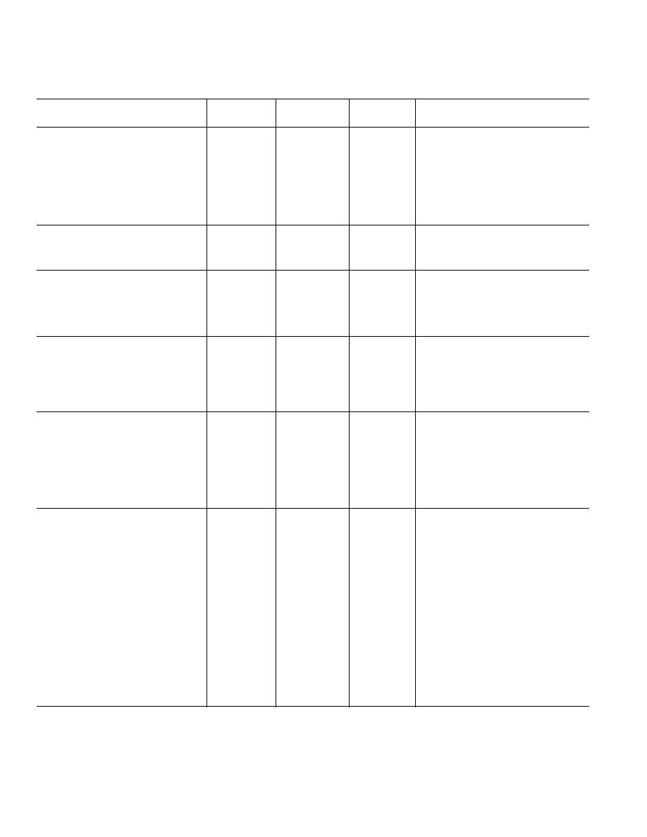
AD7224≠SPECIFICATIONS
(V
DD
= 11.4 V to 16.5 V, V
SS
= ≠5 V 10%; AGND = DGND = O V; V
REF
= +2 V to (V
DD
≠ 4 V)
1
unless otherwise noted.
All specifications T
MIN
to T
MAX
unless otherwise noted.)
DUAL SUPPLY
K, B, T
L, C, U
Parameter
Versions
2
Versions
2
Units
Conditions/Comments
STATIC PERFORMANCE
Resolution
8
8
Bits
Total Unadjusted Error
±
2
±
1
LSB max
V
DD
= +15 V
±
5%, V
REF
= +10 V
Relative Accuracy
±
1
±
1/2
LSB max
Differential Nonlinearity
±
1
±
1
LSB max
Guaranteed Monotonic
Full-Scale Error
±
3/2
±
1
LSB max
Full-Scale Temperature Coefficient
±
20
±
20
ppm/
∞
C max
V
DD
= 14 V to 16.5 V, V
REF
= +10 V
Zero Code Error
±
30
±
20
mV max
Zero Code Error Temperature Coefficient
±
50
±
30
µ
V/
∞
C typ
REFERENCE INPUT
Voltage Range
2 to (V
DD
≠ 4)
2 to (V
DD
≠ 4)
V min to V max
Input Resistance
8
8
k
min
Input Capacitance
3
100
100
pF max
Occurs when DAC is loaded with all 1s.
DIGITAL INPUTS
Input High Voltage, V
INH
2.4
2.4
V min
Input Low Voltage, V
INL
0.8
0.8
V max
Input Leakage Current
±
1
±
1
µ
A max
V
IN
= 0 V or V
DD
Input Capacitance
3
8
8
pF max
Input Coding
Binary
Binary
DYNAMIC PERFORMANCE
Voltage Output Slew Rate
3
2.5
2.5
V/
µ
s min
Voltage Output Settling Time
3
Positive Full-Scale Change
5
5
µ
s max
V
REF
= +10 V; Settling Time to
±
1/2 LSB
Negative Full-Scale Change
7
7
µ
s max
V
REF
= +10 V; Settling Time to
±
1/2 LSB
Digital Feedthrough
50
50
nV secs typ
V
REF
= 0 V
Minimum Load Resistance
2
2
k
min
V
OUT
= +10 V
POWER SUPPLIES
V
DD
Range
11.4/16.5
11.4/16.5
V min/V max
For Specified Performance
V
SS
Range
4.5/5.5
4.5/5.5
V min/V max
For Specified Performance
I
DD
@ 25
∞
C
4
4
mA max
Outputs Unloaded; V
IN
= V
INL
or V
INH
T
MIN
to T
MAX
6
6
mA max
Outputs Unloaded; V
IN
= V
INL
or V
INH
I
SS
@ 25
∞
C
3
3
mA max
Outputs Unloaded; V
IN
= V
INL
or V
INH
T
MIN
to T
MAX
5
5
mA max
Outputs Unloaded; V
IN
= V
INL
or V
INH
SWITCHING CHARACTERISTICS
3, 4
t
1
@ 25
∞
C
90
90
ns min
Chip Select/Load DAC Pulse Width
T
MIN
to T
MAX
90
90
ns min
t
2
@ 25
∞
C
90
90
ns min
Write/Reset Pulse Width
T
MIN
to T
MAX
90
90
ns min
t
3
@ 25
∞
C
0
0
ns min
Chip Select/Load DAC to Write Setup Time
T
MIN
to T
MAX
0
0
ns min
t
4
@ 25
∞
C
0
0
ns min
Chip Select/Load DAC to Write Hold Time
T
MIN
to T
MAX
0
0
ns min
t
5
@ 25
∞
C
90
90
ns min
Data Valid to Write Setup Time
T
MIN
to T
MAX
90
90
ns min
t
6
@ 25
∞
C
10
10
ns min
Data Valid to Write Hold Time
T
MIN
to T
MAX
10
10
ns min
NOTES
1
Maximum possible reference voltage.
2
Temperature ranges are as follows:
K, L Versions: ≠40
∞
C to +85
∞
C
B, C Versions: ≠40
∞
C to +85
∞
C
T, U Versions: ≠55
∞
C to +125
∞
C
3
Sample Tested at 25
∞
C by Product Assurance to ensure compliance.
4
Switching characteristics apply for single and dual supply operation.
Specifications subject to change without notice.

AD7224
REV. B
≠3≠
SINGLE SUPPLY
K, B, T
L, C, U
Parameter
Versions
2
Versions
2
Units
Conditions/Comments
STATIC PERFORMANCE
Resolution
8
8
Bits
Total Unadjusted Error
±
2
±
2
LSB max
Differential Nonlinearity
±
1
±
1
LSB max
Guaranteed Monotonic
REFERENCE INPUT
Input Resistance
8
8
k
min
Input Capacitance
3
100
100
pF max
Occurs when DAC is loaded with all 1s.
DIGITAL INPUTS
Input High Voltage, V
INH
2.4
2.4
V min
Input Low Voltage, V
INL
0.8
0.8
V max
Input Leakage Current
±
1
±
1
µ
A max
V
IN
= 0 V or V
DD
Input Capacitance
3
8
8
pF max
Input Coding
Binary
Binary
DYNAMIC PERFORMANCE
Voltage Output Slew Rate
4
2
2
V/
µ
s min
Voltage Output Settling Time
4
Positive Full-Scale Change
5
5
µ
s max
Settling Time to
±
1/2 LSB
Negative Full-Scale Change
20
20
µ
s max
Settling Time to
±
1/2 LSB
Digital Feedthrough
3
50
50
nV secs typ
V
REF
= 0 V
Minimum Load Resistance
2
2
k
min
V
OUT
= +10 V
POWER SUPPLIES
V
DD
Range
14.25/15.75
14.25/15.75
V min/V max
For Specified Performance
I
DD
@ 25
∞
C
4
4
mA max
Outputs Unloaded; V
IN
= V
INL
or V
INH
T
MIN
to T
MAX
6
6
mA max
Outputs Unloaded; V
IN
= V
INL
or V
INH
SWITCHING CHARACTERISTICS
3, 4
t
1
@ 25
∞
C
90
90
ns min
Chip Select/Load DAC Pulse Width
T
MIN
to T
MAX
90
90
ns min
t
2
@ 25
∞
C
90
90
ns min
Write/Reset Pulse Width
T
MIN
to T
MAX
90
90
ns min
t
3
@ 25
∞
C
0
0
ns min
Chip Select/Load DAC to Write Setup Time
T
MIN
to T
MAX
0
0
ns min
t
4
@ 25
∞
C
0
0
ns min
Chip Select/Load DAC to Write Hold Time
T
MIN
to T
MAX
0
0
ns min
t
5
@ 25
∞
C
90
90
ns min
Data Valid to Write Setup Time
T
MIN
to T
MAX
90
90
ns min
t
6
@ 25
∞
C
10
10
ns min
Data Valid to Write Hold Time
T
MIN
to T
MAX
10
10
ns min
NOTES
1
Maximum possible reference voltage.
2
Temperature ranges are as follows:
AD7224KN, LN: 0
∞
C to +70
∞
C
AD7224BQ, CQ: ≠25
∞
C to +85
∞
C
AD7224TD, UD: ≠55
∞
C to +125
∞
C
3
See Terminology.
4
Sample tested at 25
∞
C by Product Assurance to ensure compliance.
Specifications subject to change without notice.
(V
DD
= +15 V 5%; V
SS
= AGND = DGND = O V; V
REF
= +10 V
1
unless otherwise noted.
All specifications T
MIN
to T
MAX
unless otherwise noted.)
AD7224
REV. B
≠4≠
ABSOLUTE MAXIMUM RATINGS
1
V
DD
to AGND . . . . . . . . . . . . . . . . . . . . . . . . . . ≠0.3 V, +17 V
V
DD
to DGND . . . . . . . . . . . . . . . . . . . . . . . . . . ≠0.3 V, +17 V
V
DD
to V
SS
. . . . . . . . . . . . . . . . . . . . . . . . . . . . . ≠0.3 V, +24 V
AGND to DGND . . . . . . . . . . . . . . . . . . . . . . . . ≠0.3 V, V
DD
Digital Input Voltage to DGND . . . . . . . ≠0.3 V, V
DD
+ 0.3 V
V
REF
to AGND . . . . . . . . . . . . . . . . . . . . ≠0.3 V, V
DD
+ 0.3 V
V
OUT
to AGND
2
. . . . . . . . . . . . . . . . . . . . . . . . . . . . V
SS
, V
DD
Power Dissipation (Any Package) to +75
∞
C . . . . . . . . 450 mW
Derates above 75
∞
C by . . . . . . . . . . . . . . . . . . . . . 6 mW/
∞
C
Operating Temperature
Commercial (K, L Versions) . . . . . . . . . . . ≠40
∞
C to +85
∞
C
Industrial (B, C Versions) . . . . . . . . . . . . . ≠40
∞
C to +85
∞
C
Extended (T, U Versions) . . . . . . . . . . . . ≠55
∞
C to +125
∞
C
Storage Temperature . . . . . . . . . . . . . . . . . . ≠65
∞
C to +150
∞
C
Lead Temperature (Soldering, 10 secs) . . . . . . . . . . . +300
∞
C
NOTES
1
Stresses above those listed under "Absolute Maximum Ratings" may cause
permanent damage to the device. This is a stress rating only and functional
operation of the device at these or any other conditions above those indicated in
the operational sections of this specification is not implied. Exposure to absolute
maximum rating conditions for extended periods may affect device reliability.
2
The outputs may be shorted to AGND provided that the power dissipation of the
package is not exceeded. Typically short circuit current to AGND is 60 mA.
ORDERING GUIDE
Total
Temperature
Unadjusted
Package
Model
1
Range
Error (LSB)
Option
2
AD7224KN
≠40
∞
C to +85
∞
C
±
2 max
N-18
AD7224LN
≠40
∞
C to +85
∞
C
±
1 max
N-18
AD7224KP
≠40
∞
C to +85
∞
C
±
2 max
P-20A
AD7224LP
≠40
∞
C to +85
∞
C
±
1 max
P-20A
AD7224KR-1
≠40
∞
C to +85
∞
C
±
2 max
R-20
AD7224LR-1
≠40
∞
C to +85
∞
C
±
1 max
R-20
AD7224KR-18
≠40
∞
C to +85
∞
C
±
2 max
R-18
AD7224LR-18
≠40
∞
C to +85
∞
C
±
1 max
R-18
AD7224BQ
≠40
∞
C to +85
∞
C
±
2 max
Q-18
AD7224CQ
≠40
∞
C to +85
∞
C
±
1 max
Q-18
AD7224TQ
≠55
∞
C to +125
∞
C
±
2 max
Q-18
AD7224UQ
≠55
∞
C to +125
∞
C
±
1 max
Q-18
AD7224TE
≠55
∞
C to +125
∞
C
±
2 max
E-20A
AD7224UE
≠55
∞
C to +125
∞
C
±
1 max
E-20A
NOTES
1
To order MIL-STD-883 processed parts, add /883B to part number.
Contact your local sales office for military data sheet.
2
E = Leadless Ceramic Chip Carrier; N = Plastic DIP;
P = Plastic Leaded Chip Carrier; Q = Cerdip; R = SOIC.
WARNING!
ESD SENSITIVE DEVICE
CAUTION
ESD (electrostatic discharge) sensitive device. Electrostatic charges as high as 4000 V readily
accumulate on the human body and test equipment and can discharge without detection.
Although the AD7224 features proprietary ESD protection circuitry, permanent damage may
occur on devices subjected to high energy electrostatic discharges. Therefore, proper ESD
precautions are recommended to avoid performance degradation or loss of functionality.
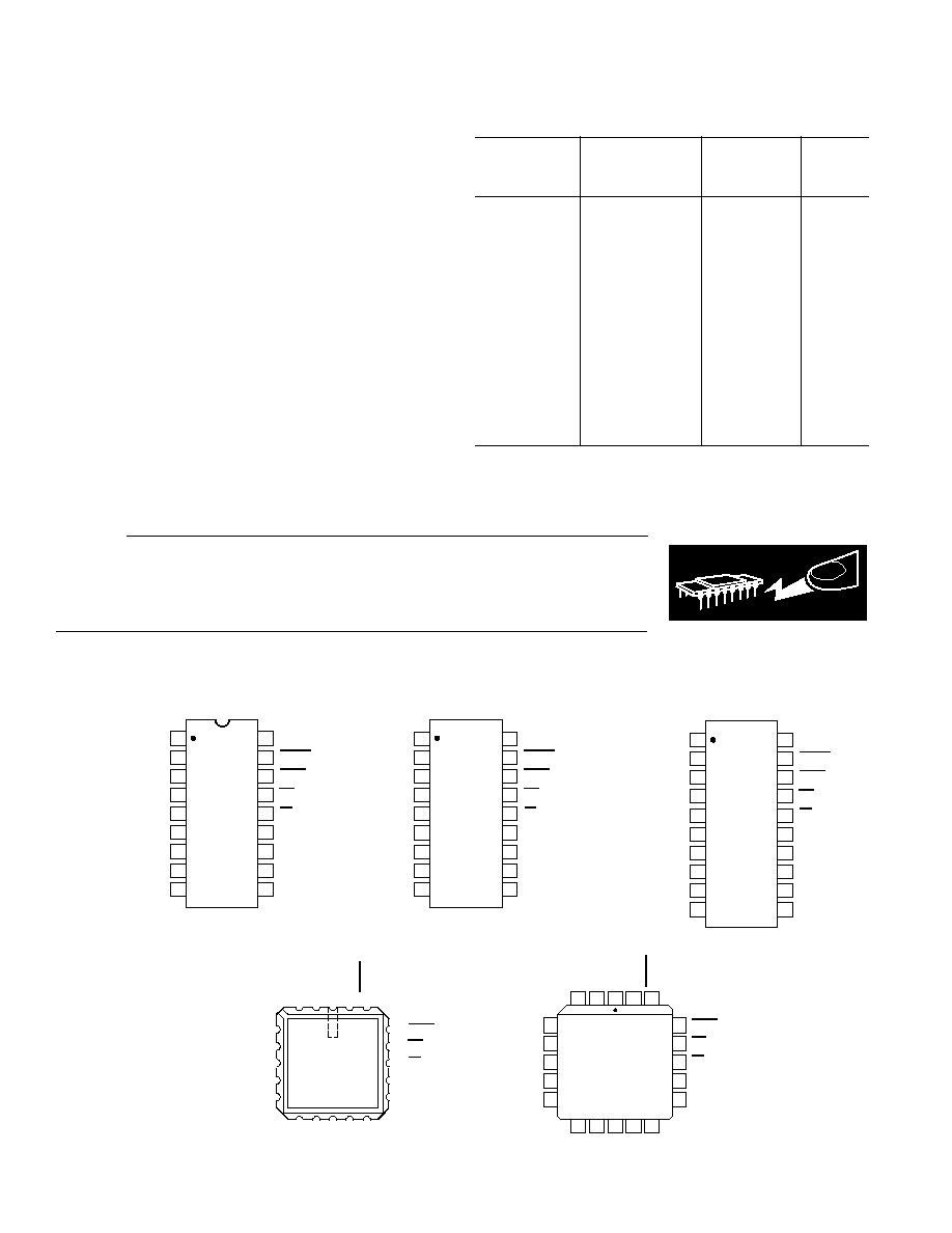
PIN CONFIGURATIONS
DIP and SOIC
(SOIC)
(SOIC)
V
SS
V
OUT
V
DD
RESET
DGND
(MSB) DB7
DB6
DB0 (LSB)
DB1
V
REF
AGND
LDAC
DB5
DB2
DB4
DB3
CS
WR
1
2
18
17
5
6
7
14
13
12
3
4
16
15
8
11
9
10
TOP VIEW
(Not to Scale)
AD7224
V
SS
V
OUT
V
DD
RESET
DGND
(MSB) DB7
DB6
DB0 (LSB)
DB1
V
REF
AGND
LDAC
DB5
DB2
DB4
DB3
CS
WR
1
2
18
17
5
6
7
14
13
12
3
4
16
15
8
11
9
10
TOP VIEW
(Not to Scale)
AD7224
R-18
NC = NO CONNECT
V
SS
V
OUT
V
DD
RESET
DGND
(MSB) DB7
DB6
CS
DB0 (LSB)
DB1
V
REF
AGND
LDAC
WR
DB5
DB2
DB4
DB3
NC
NC
1
2
20
19
5
6
7
16
15
14
3
4
18
17
8
13
9
12
10
11
TOP VIEW
(Not to Scale)
AD7224
R-20
LCCC
PLCC
NC = NO CONNECT
V
REF
AGND
DB6
DGND
(MSB) DB7
V
OUT
V
SS
RESET
NC
V
DD
DB5
DB4
DB2
NC
DB3
LDAC
WR
DB1
CS
DB0 (LSB)
19
3
1
2
20
4
5
8
6
7
12 13
9
11
10
18
17
14
16
15
TOP VIEW
(Not to Scale)
AD7224
NC = NO CONNECT
V
REF
AGND
DB6
DGND
(MSB) DB7
V
OUT
V
SS
RESET
NC
V
DD
DB5
DB4
DB2
NC
DB3
LDAC
WR
DB1
CS
DB0 (LSB)
19
3
1
2
20
4
5
8
6
7
12
13
9
11
10
18
17
14
16
15
TOP VIEW
(Not to Scale)
AD7224
AD7224
REV. B
≠5≠
V
OUT
= D ∑ V
REF
where D is a fractional representation of the digital input code
and can vary from 0 to 255/256.
OP-AMP SECTION
The voltage-mode D/A converter output is buffered by a unity
gain noninverting CMOS amplifier. This buffer amplifier is
capable of developing +10 V across a 2 k
load and can drive
capacitive loads of 3300 pF.
The AD7224 can be operated single or dual supply resulting in
different performance in some parameters from the output am-
plifier. In single supply operation (V
SS
= 0 V = AGND) the sink
capability of the amplifier, which is normally 400
µ
A, is reduced
as the output voltage nears AGND. The full sink capability of
400
µ
A is maintained over the full output voltage range by tying
V
SS
to ≠5 V. This is indicated in Figure 2.
500
0
10
300
100
2
200
0
400
8
6
4
V
OUT
≠ Volts
I
SINK
≠
µ
A
V
SS
= ≠5V
V
SS
= 0V
V
DD
= +15V
T
A
= 25
∞
C
Figure 2. Variation of I
SINK
with V
OUT
Settling-time for negative-going output signals approaching
AGND is similarly affected by V
SS
. Negative-going settling-time
for single supply operation is longer than for dual supply opera-
tion. Positive-going settling-time is not affected by V
SS
.
Additionally, the negative V
SS
gives more headroom to the out-
put amplifier which results in better zero code performance and
improved slew-rate at the output, than can be obtained in the
single supply mode.
DIGITAL SECTION
The AD7224 digital inputs are compatible with either TTL or
5 V CMOS levels. All logic inputs are static-protected MOS
gates with typical input currents of less than 1 nA. Internal in-
put protection is achieved by an on-chip distributed diode be-
tween DGND and each MOS gate. To minimize power supply
currents, it is recommended that the digital input voltages be
driven as close to the supply rails (V
DD
and DGND) as practi-
cally possible.
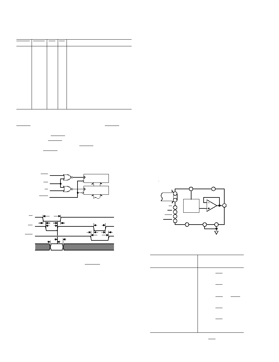
INTERFACE LOGIC INFORMATION
Table I shows the truth table for AD7224 operation. The part
contains two registers, an input register and a DAC register. CS
and WR control the loading of the input register while LDAC
and WR control the transfer of information from the input regis-
ter to the DAC register. Only the data held in the DAC register
will determine the analog output of the converter.
All control signals are level-triggered and therefore either or
both registers may be made transparent; the input register by
keeping CS and WR "LOW", the DAC register by keeping
LDAC
and WR "LOW". Input data is latched on the rising
edge of WR.
TERMINOLOGY
TOTAL UNADJUSTED ERROR
Total Unadjusted Error is a comprehensive specification which
includes full-scale error, relative accuracy and zero code error.
Maximum output voltage is V
REF
≠ 1 LSB (ideal), where 1 LSB
(ideal) is V
REF
/256. The LSB size will vary over the V
REF
range.
Hence the zero code error, relative to the LSB size, will increase
as V
REF
decreases. Accordingly, the total unadjusted error,
which includes the zero code error, will also vary in terms of
LSBs over the V
REF
range. As a result, total unadjusted error is
specified for a fixed reference voltage of +10 V.
RELATIVE ACCURACY
Relative Accuracy or endpoint nonlinearity is a measure of the
maximum deviation from a straight line passing through the
endpoints of the DAC transfer function. It is measured after al-
lowing for zero code error and full-scale error and is normally
expressed in LSBs or as a percentage of full-scale reading.
DIFFERENTIAL NONLINEARITY
Differential Nonlinearity is the difference between the measured
change and the ideal 1 LSB change between any two adjacent
codes. A specified differential nonlinearity of
±
1 LSB max over
the operating temperature range ensures monotonicity.
DIGITAL FEEDTHROUGH
Digital Feedthrough is the glitch impulse transferred to the out-
put due to a change in the digital input code. It is specified in
nV secs and is measured at V
REF
= 0 V.
FULL-SCALE ERROR
Full-Scale Error is defined as:
Measured Value ≠ Zero Code Error ≠ Ideal Value
CIRCUIT INFORMATION
D/A SECTION
The AD7224 contains an 8-bit voltage-mode digital-to-analog
converter. The output voltage from the converter has the same
polarity as the reference voltage, allowing single supply opera-
tion. A novel DAC switch pair arrangement on the AD7224 al-
lows a reference voltage range from +2 V to +12.5 V.
The DAC consists of a highly stable, thin-film, R-2R ladder and
eight high speed NMOS single pole, double-throw switches.
The simplified circuit diagram for this DAC is shown in
Figure 1.
V
OUT
R
R
R
2R
2R
2R
2R
2R
DB0
DB0
DB0
DB0
V
REF
AGND
SHOWN FOR ALL 1's ON DAC
Figure 1. D/A Simplified Circuit Diagram
The input impedance at the V
REF
pin is code dependent and can
vary from 8 k
minimum to infinity. The lowest input imped-
ance occurs when the DAC is loaded with the digital code
01010101. Therefore, it is important that the reference presents
a low output impedance under changing load conditions. The
nodal capacitance at the reference terminals is also code depen-
dent and typically varies from 25 pF to 50 pF.
The V
OUT
pin can be considered as a digitally programmable
voltage source with an output voltage of:
AD7224
REV. B
≠6≠
Table I. AD7224 Truth Table
RESET
LDAC
WR
CS
Function
H
L
L
L
Both Registers are Transparent
H
X
H
X
Both Registers are Latched
H
H
X
H
Both Registers are Latched
H
H
L
L
Input Register Transparent
H
H
g
L
Input Register Latched
H
L
L
H
DAC Register Transparent
H
L
g
H
DAC Register Latched
L
X
X
X
Both Registers Loaded
With All Zeros
g
H
H
H
Both Register Latched With All Zeros
and Output Remains at Zero
g
L
L
L
Both Registers are Transparent and
Output Follows Input Data
H = High State, L = Low State, X = Don't Care.
All control inputs are level triggered.
The contents of both registers are reset by a low level on the
RESET
line. With both registers transparent, the RESET line
functions like a zero override with the output brought to 0 V for
the duration of the RESET pulse. If both registers are latched, a
"LOW" pulse on RESET will latch all 0s into the registers and
the output remains at 0 V after the RESET line has returned
"HIGH". The RESET line can be used to ensure power-up to
0 V on the AD7224 output and is also useful, when used as a
zero override, in system calibration cycles. Figure 3 shows the
input control logic for the AD7224.
INPUT DATA
LDAC
WR
CS
RESET
DAC
REGISTER
INPUT
REGISTER
Figure 3. Input Control Logic
t
2
t
1
t
2
t
1
t
4
t
3
t
3
t
4
DATA
VALID
t
5
t
6
DATA
IN
CS
WR
LDAC
NOTES:
1. ALL INPUT SIGNAL RISE AND FALL TIMES MEASURED FROM 10% TO 90% OF V
DD
.
tr = tf = 20ns OVER V
DD
RANGE
2. TIMING MEASUREMENT REFERENCE LEVEL IS
V
INH
+ V
INL
2
Figure 4. Write Cycle Timing Diagram
SPECIFICATION RANGES
For the DAC to maintain specified accuracy, the reference volt-
age must be at least 4 V below the V
DD
power supply voltage.
This voltage differential is required for correct generation of bias
voltages for the DAC switches.
With dual supply operation, the AD7224 has an extended V
DD
range from +12 V
±
5% to +15 V
±
10% (i.e., from +11.4 V to
+16.5 V). Operation is also specified for a single V
DD
power
supply of +15 V
±
5%.
Performance is specified over a wide range of reference voltages
from 2 V to (V
DD
≠ 4 V) with dual supplies. This allows a range
of standard reference generators to be used such as the AD580,
a +2.5 V bandgap reference and the AD584, a precision +10 V
reference. Note that in order to achieve an output voltage range
of 0 V to +10 V, a nominal +15 V
±
5% power supply voltage is
required by the AD7224.
GROUND MANAGEMENT
AC or transient voltages between AGND and DGND can cause
noise at the analog output. This is especially true in micropro-
cessor systems where digital noise is prevalent. The simplest
method of ensuring that voltages at AGND and DGND are
equal is to tie AGND and DGND together at the AD7224. In
more complex systems where the AGND and DGND intertie is
on the backplane, it is recommended that two diodes be con-
nected in inverse parallel between the AD7224 AGND and
DGND pins (IN914 or equivalent).
Applying the AD7224
UNIPOLAR OUTPUT OPERATION
This is the basic mode of operation for the AD7224, with the
output voltage having the same positive polarity as V
REF
. The
AD7224 can be operated single supply (V
SS
= AGND) or with
positive/negative supplies (see op-amp section which outlines
the advantages of having negative V
SS
). Connections for the uni-
polar output operation are shown in Figure 5. The voltage at
V
REF
must never be negative with respect to DGND. Failure to
observe this precaution may cause parasitic transistor action and
possible device destruction. The code table for unipolar output
operation is shown in Table II.
DAC
DB7
DB0
3
V
DD
V
REF
CS
WR
LDAC
RESET
V
SS
AGND
DGND
AD7224
V
OUT
DATA
(8-BIT)
Figure 5. Unipolar Output Circuit
Table III. Unipolar Code Table
DAC Register Contents
MSB
LSB
Analog Output
1 1 1 1
1 1 1 1
+
V
REF
255
256
1 0 0 0
0 0 0 1
+
V
REF
129
256
1 0 0 0
0 0 0 0
+
V
REF
128
256
= +
V
REF
2
0 1 1 1
1 1 1 1
+
V
REF
127
256
0 0 0 0
0 0 0 1
+
V
REF
1
256
0 0 0 0
0 0 0 0
0 V
Note: 1 LSB
=
V
REF
(
)
2
-
8
( )
=
V
REF
1
256

AD7224
REV. B
≠7≠
BIPOLAR OUTPUT OPERATION
The AD7224 can be configured to provide bipolar output op-
eration using one external amplifier and two resistors. Figure 6
shows a circuit used to implement offset binary coding. In this
case
V
O
=
1
+
R2
R1
∑ D V
REF
(
)
≠
R2
R1
∑ V
REF
(
)
With R1 = R2
V
O
= (2 D ≠ 1) ∑ V
REF
where D is a fractional representation of the digital word in
the DAC register.
Mismatch between R1 and R2 causes gain and offset errors;
therefore, these resistors must match and track over tempera-
ture. Once again, the AD7224 can be operated in single supply
or from positive/negative supplies. Table III shows the digital
code versus output voltage relationship for the circuit of Figure
6 with R1 = R2.
+15V
+15V
V
REF
R1
R2
V
OUT
R1, R2 = 10k
±
0.1%
DAC
DB7
DB0
3
V
DD
V
REF
CS
WR
LDAC
RESET
V
SS
AGND
DGND
AD7224
V
OUT
DATA
(8-BIT)
Figure 6. Bipolar Output Circuit
Table III. Bipolar (Offset Binary) Code Table
DAC Register Contents
MSB
LSB
Analog Output
1 1 1 1
1 1 1 1
+
V
REF
127
128
1 0 0 0
0 0 0 1
+
V
REF
1
128
1 0 0 0
0 0 0 0
0 V
0 1 1 1
1 1 1 1
≠V
REF
1
128
0 0 0 0
0 0 0 1
≠V
REF
127
128
0 0 0 0
0 0 0 0
≠V
REF
128
128
=
≠V
REF
AGND BIAS
The AD7224 AGND pin can be biased above system GND
(AD7224 DGND) to provide an offset "zero" analog output
voltage level. Figure 7 shows a circuit configuration to achieve
this. The output voltage, V
OUT
, is expressed as:
V
OUT
= V
BIAS
+ D
∑
(V
IN
)
where D is a fractional representation of the digital word in
DAC register and can vary from 0 to 255/256.
For a given V
IN
, increasing AGND above system GND will re-
duce the effective V
DD
≠V
REF
which must be at least 4 V to en-
sure specified operation. Note that V
DD
and V
SS
for the AD7224
must be referenced to DGND.
DAC
V
DD
V
REF
V
SS
AGND
DGND
AD7224
V
OUT
V
IN
V
IN
V
BIAS
Figure 7. AGND Bias Circuit
MICROPROCESSOR INTERFACE
8085A
8088
A15
A8
ALE
AD0
AD7
ADDRESS
DECODE
LATCH
EN
AD7224*
WR
DB7
DB0
LDAC
WR
ADDRESS BUS
ADDRESS DATA BUS
*LINEAR CIRCUITRY OMITTED FOR CLARITY
CS
Figure 8. AD7224 to 8085A/8088 Interface
D0
D7
DATA BUS
*LINEAR CIRCUITRY OMITTED FOR CLARITY
E OR
2
D0
D7
E OR
2
R/W
A15
A0
6809
6502
ADDRESS
DECODE
EN
ADDRESS BUS
LDAC
WR
CS
DB7
DB0
AD7224*
Figure 9. AD7224 to 6809/6502 Interface
Z-80
A15
A0
D0
D7
AD7224*
DB7
DB0
LDAC
WR
ADDRESS BUS
DATA BUS
*LINEAR CIRCUITRY OMITTED FOR CLARITY
ADDRESS
DECODE
CS
WR
Figure 10. AD7224 to Z-80 Interface
68008
A23
A1
D0
D7
AD7224*
DB7
DB0
LDAC
WR
ADDRESS BUS
DATA BUS
*LINEAR CIRCUITRY OMITTED FOR CLARITY
ADDRESS
DECODE
CS
R/W
DTACK
Figure 11. AD7224 to 68008 Interface

AD7224
REV. B
≠8≠
OUTLINE DIMENSIONS
Dimensions shown in inches and (mm).
C836a≠10≠10/84
PRINTED IN U.S.A.
18-Pin Plastic (Suffix N)
18-Pin Ceramic (Suffix D)
PLCC Package
P-20A
0.048 (1.21)
0.042 (1.07)
0.356 (9.04)
0.350 (8.89)
SQ
0.395 (10.02)
0.385 (9.78)
SQ
0.048 (1.21)
0.042 (1.07)
0.050
(1.27)
BSC
0.020
(0.50)
R
19
3
TOP VIEW
18
14
9
8
PIN 1
IDENTIFIER
4
13
0.110 (2.79)
0.085 (2.16)
0.032 (0.81)
0.026 (0.66)
0.021 (0.53)
0.013 (0.33)
0.056 (1.42)
0.042 (1.07)
0.025 (0.63)
0.015 (0.38)
0.040 (1.01)
0.025 (0.64)
0.180 (4.57)
0.165 (4.19)
0.330 (8.38)
0.290 (7.37)
LCCC Package
E-20A
0.358
(9.09)
MAX
SQ
0.088 (2.24)
0.054 (1.37)
0.100 (2.54)
0.064 (1.63)
0.358 (9.09)
0.342 (8.69)
SQ
0.075
(1.91)
REF
0.075
(1.91)
REF
0.011 (0.28)
0.007 (0.18)
R TYP
BOTTOM
VIEW
0.015 (0.38)
MIN
1
20
13
9
0.028 (0.71)
0.022 (0.56)
0.095 (2.41)
0.075 (1.90)
0.200 (5.08)
BSC
0.100
(2.54)
BSC
0.055 (1.40)
0.045 (1.14)
45
∞
TYP
0.150
(3.81)
BSC
0.050
(1.27)
BSC
18-Pin Cerdip (Suffix Q)
18-Lead SOIC
(R-18)
PIN 1
0.2992 (7.60)
0.2914 (7.40)
0.4193 (10.65)
0.3937 (10.00)
1
18
10
9
0.4625 (11.75)
0.4469 (11.35)
0.0192 (0.49)
0.0138 (0.35)
0.0500
(1.27)
BSC
0.1043 (2.65)
0.0926 (2.35)
0.0118 (0.30)
0.0040 (0.10)
0.0125 (0.32)
0.0091 (0.23)
0.0500 (1.27)
0.0157 (0.40)
8
∞
0
∞
0.0291 (0.74)
0.0098 (0.25)
x 45
∞
20-Lead SOIC
(R-20)
PIN 1
0.2992 (7.60)
0.2914 (7.40)
0.4193 (10.65)
0.3937 (10.00)
1
20
11
10
0.0125 (0.32)
0.0091 (0.23)
0.0500 (1.27)
0.0157 (0.40)
8
∞
0
∞
0.0291 (0.74)
0.0098 (0.25)
x 45
∞
0.5118 (13.00)
0.4961 (12.60)
0.0192 (0.49)
0.0138 (0.35)
0.0500
(1.27)
BSC
0.0118 (0.30)
0.0040 (0.10)
0.1043 (2.65)
0.0926 (2.35)