
REV. A
Information furnished by Analog Devices is believed to be accurate and
reliable. However, no responsibility is assumed by Analog Devices for its
use, nor for any infringements of patents or other rights of third parties
which may result from its use. No license is granted by implication or
otherwise under any patent or patent rights of Analog Devices.
a
LC
2
MOS
12-Bit Serial DACPORT
AD7243
FUNCTIONAL BLOCK DIAGRAM
INPUT SHIFT REGISTER
DAC LATCH
12 - BIT DAC
12
12
AGND
DGND
REFOUT
REFIN
SDIN CLR
SCLK
DCEN SDO
R
OFS
V
OUT
V
SS
V
DD
2R
2R
AD7243
BIN/
COMP
SYNC LDAC
FEATURES
12-Bit CMOS DAC with
On-Chip Voltage Reference
Output Amplifier
Three Selectable Output Ranges
�5 V to +5 V, 0 V to +5 V, 0 V to +10 V
Serial Interface
300 kHz DAC Update Rate
Small Size: 16-Lead DIP or SOIC
Nonlinearity: 1/2 LSB T
MIN
to T
MAX
Low Power Dissipation: 100 mW Typical
APPLICATIONS
Process Control
Industrial Automation
Digital Signal Processing Systems
Input/Output Ports
GENERAL DESCRIPTION
The AD7243 is a complete 12-bit, voltage output, digital-to-
analog converter with output amplifier and Zener voltage refer-
ence on a monolithic CMOS chip. No external trims are
required to achieve full specified performance.
The output amplifier is capable of developing +10 V across a
2 k
load. The output voltage ranges with single supply opera-
tion are 0 V to +5 V or 0 V to +10 V, while an additional bipo-
lar
�5 V output range is available with dual supplies. The ranges
are selected using the internal gain resistor.
The data format is natural binary in both unipolar ranges, while
either offset binary or two's complement format may be selected
in the bipolar range. A
CLR function is provided which sets the
output to 0 V in both unipolar ranges and in the two's comple-
ment bipolar range, while with offset binary data format, the
output is set to �REFIN. This function is useful as a power-on
reset as it allows the output to be set to a known voltage level.
The AD7243 features a fast versatile serial interface which
allows easy connection to both microcomputers and 16-bit digi-
tal signal processors with serial ports. The serial data may be
applied at rates up to 5 MHz allowing a DAC update rate of
300 kHz. A serial data output capability is also provided which
allows daisy chaining in multi-DAC systems. This feature allows
any number of DACs to be used in a system with a simple
4-wire interface. All DACs may be updated simultaneously
using
LDAC.
The AD7243 is fabricated on Linear Compatible CMOS
(LC
2
MOS), an advanced, mixed technology process. It is pack-
aged in 16-lead DIP and 16-lead SOIC packages.
PRODUCT HIGHLIGHTS
1. Complete 12-Bit DACPORT
�
The AD7243 is a complete, voltage output, 12-bit DAC on
a single chip. The single chip design is inherently more
reliable than multichip designs.
2. Single or Dual Supply Operation.
3. Minimum 3-wire interface to most DSP processors.
4. DAC Update Rate�300 kHz.
5. Serial Data Output allows easy daisy-chaining in multiple
DAC systems.
One Technology Way, P.O. Box 9106, Norwood, MA 02062-9106, U.S.A.
Tel: 781/329-4700
World Wide Web Site: http://www.analog.com
Fax: 781/326-8703
� Analog Devices, Inc., 2000
DACPORT is a registered trademark of Analog Devices, Inc.

AD7243�SPECIFICATIONS
Parameter
A
2
B
2
S
2
Unit
Test Conditions/Comments
STATIC PERFORMANCE
Resolution
12
12
12
Bits
Relative Accuracy
3
�1
�1/2
�1
LSB max
Differential Nonlinearity
3
�0.9
�0.9
�0.9
LSB max
Guaranteed Monotonic
Unipolar Offset Error
3
�4
�4
�5
LSB max
V
SS
= 0 V or �12 V to �15 V
1
; DAC Latch
Contents All 0s
Bipolar Zero Error
3
�5
�5
�6
LSB max
V
SS
= �12 V to �15 V
1
; DAC Latch Contents All 0s
Full-Scale Error
3, 4
�6
�6
�7
LSB max
Full-Scale Temperature Coefficient
5
�5
�5
�5
ppm of FSR/
Guaranteed By Process
�C typ
REFERENCE OUTPUT
Reference Output Range, REFOUT
4.95/5.05
4.95/5.05
4.95/5.05
V min/V max
Reference Temperature Coefficient
5
�25
�25
�30
ppm/
�C typ
Guaranteed By Process
Reference Load Change
(
REFOUT
VS
. I
L
)
�1
�1
�1
mV max
Reference Load Current (I
L
) Change (0�100
�A)
REFERENCE INPUT
Reference Input Range, REFIN
4.95/5.05
4.95/5.05
4.95/5.05
V min/V max
5 V
�1% for Specified Performance
Input Current
5
5
5
�A max
DIGITAL INPUTS
Input High Voltage, V
INH
2.4
2.4
2.4
V min
Input Low Voltage, V
INL
0.8
0.8
0.8
V max
Input Current, I
IN
�1
�1
�1
�A max
V
IN
= 0 V to V
DD
Input Capacitance
5
8
8
8
pF max
DIGITAL OUTPUT
Serial Data Out (SDO)
Output Low Voltage, V
OL
0.4
0.4
0.4
V max
I
SINK
= 1.6 mA
Output High Voltage, V
OH
4.0
4.0
4.0
V min
I
SOURCE
= 400
�A
ANALOG OUTPUT
Output Range Resistor, R
OFS
15/30
15/30
15/30
k
min/max
Typically 20 k . Guaranteed By Process
Output Voltage Ranges
6
+5, +10
+5, +10
+5, +10
V
Single Supply; V
SS
= 0 V
Output Voltage Ranges
6
+5, +10,
�5 +5, +10, �5 +5, +10, �5
V
Dual Supply; V
SS
= �12 V to �15 V
DC Output Impedance
5
0.5
0.5
0.5
typ
AC CHARACTERISTICS
5
Voltage Output Settling-Time
Settling Time to Within
�1/2 LSB of Final Value
Positive Full-Scale Change
10
10
10
�s max
Typically 4
�s
Negative Full-Scale Change
10
10
10
�s max
Typically 5
�s
Digital-to-Analog Glitch Impulse
3
30
30
30
nV secs typ
DAC Latch Contents Toggled Between All 0s
and All 1s
Digital Feedthrough
3
10
10
10
nV secs typ
LDAC = High
POWER REQUIREMENTS
V
DD
Range
+10.8/+16.5 +10.8/+16.5
+11.4/+15.75
V min/V max
For Specified Performance Unless Otherwise Stated
V
SS
Range (Dual Supplies)
�10.8/�16.5
�10.8/�16.5
�11.4/�15.75
V min/V max
For Specified Performance Unless Otherwise Stated
I
DD
10
10
10
mA max
Output Unloaded; Typically 7 mA
I
SS
(Dual Supplies)
2
2
2
mA max
Output Unloaded; Typically 1 mA
NOTES
1
Power Supply Tolerance A, B Versions:
�10%; S Version: �5%.
2
Temperature ranges are as follows: A, B Versions: �40
�C to +85�C; S Version: �55�C to +125�C.
3
See terminology.
4
Measured with respect to REFIN and includes unipolar/bipolar offset error.
5
Guaranteed by design and characterization, not production tested.
6
0 V to +10 V output range is available only with V
DD
+14.25 V.
Specifications subject to change without notice.
(V
DD
= +12 V to +15 V,
1
V
SS
= 0 V or �12 V to �15 V,
1
AGND = DGND = O V, REFIN = +5 V,
R
L
= 2 k
, C
L
= 100 pF to AGND. All Specifications T
MIN
to T
MAX
unless otherwise noted.)
�2�
REV. A

REV. A
�3�
AD7243
Limit at +25 C, T
MIN
, T
MAX
Parameter
(All Versions)
Units
Conditions/Comments
t
1
3
200
ns min
SCLK Cycle Time
t
2
15
ns min
SYNC to SCLK Falling Edge Setup Time
t
3
70
ns min
SYNC to SCLK Hold Time
t
4
0
ns min
Data Setup Time
t
5
40
ns min
Data Hold Time
t
6
0
ns min
SYNC High to LDAC Low
t
7
20
ns min
LDAC Pulsewidth
t
8
0
ns min
LDAC High to SYNC Low
t
9
20
ns min
CLR Pulsewidth
t
10
4, 5
160
ns max
SCLK Falling Edge to SDO Valid
t
11
4, 6
>t
5
ns min
SCLK Falling Edge to SDO Invalid
NOTES
1
Sample tested at +25
�C to ensure compliance. All input signals are specified with tr = tf = 5 ns (10% to 90% of 5 V) and timed from a voltage level of 1.6 V.
2
See Figures 7 & 8.
3
SCLK mark/space ratio range is 40/60 to 60/40.
4
SDO load capacitance is no greater than 50 pF.
5
At 25
�C t
10
is 130 ns max.
6
Guaranteed by design.
ORDERING GUIDE
Model
Temperature Range
Relative Accuracy
Package Option
1
AD7243AN
�40
�C to +85�C
�1 LSB
N-16
AD7243BN
�40
�C to +85�C
�1/2 LSB
N-16
AD7243AR
�40
�C to +85�C
�1 LSB
R-16
AD7243BR
�40
�C to +85�C
�1/2 LSB
R-16
AD7243AQ
�40
�C to +85�C
�1 LSB
Q-16
AD7243BQ
�40
�C to +85�C
�1/2 LSB
Q-16
AD7243SQ
2
�55
�C to +125�C
�1 LSB
Q-16
NOTES
1
N = Plastic DIP; R = SOIC; Q = Cerdip.
2
Available to /883B processing only. Contact your local sales office for military data sheet.
ABSOLUTE MAXIMUM RATINGS
1
(T
A
= +25
�C unless otherwise noted)
V
DD
to AGND, DGND . . . . . . . . . . . . . . . . . �0.3 V to +17 V
V
SS
to AGND, DGND . . . . . . . . . . . . . . . . . +0.3 V to �17 V
AGND to DGND . . . . . . . . . . . . . . . . �0.3 V to V
DD
+ 0.3 V
V
OUT
2
to AGND . . . . . . . . . . . . . . . . . . . �6 V to V
DD
+ 0.3 V
REFOUT to AGND . . . . . . . . . . . . . . . . . . . . . . . 0 V to V
DD
REFIN to AGND . . . . . . . . . . . . . . . . �0.3 V to V
DD
+ 0.3 V
Digital Inputs to DGND . . . . . . . . . . . �0.3 V to V
DD
+ 0.3 V
SDO to DGND . . . . . . . . . . . . . . . . . . �0.3 V to V
DD
+ 0.3 V
Operating Temperature Range
Industrial (A, B Versions) . . . . . . . . . . . . . �40
�C to +85�C
Extended (S Version) . . . . . . . . . . . . . . . . �55
�C to +125�C
TIMING CHARACTERISTICS
1, 2
Storage Temperature Range . . . . . . . . . . . . �65
�C to +150�C
Lead Temperature (Soldering, 10 secs) . . . . . . . . . . . . +300
�C
Power Dissipation (Any Package) to +75
�C . . . . . . . 450 mW
Derates above +75
�C by . . . . . . . . . . . . . . . . . . . . . 6 mW/�C
NOTES
1
Stresses above those listed under Absolute Maximum Ratings may cause perma-
nent damage to the device. This is a stress rating only; functional operation of the
device at these or any other conditions above those listed in the operational sections
of this specification is not implied. Exposure to absolute maximum rating condi-
tions for extended periods may affect device reliability. Only one Absolute
Maximum Rating may be applied at any time.
2
The outputs may be shorted to voltages in this range provided the power dissipation
of the package is not exceeded. Short circuit current is typically 80 mA.
(V
DD
= +10.8 V to +16.5 V, V
SS
= 0 V or �10.8 V to �16.5 V, AGND = DGND = 0 V,
R
L
= 2 k
, C
L
= 100 pF. All Specifications T
MIN
to T
MAX
unless otherwise noted.)
CAUTION
ESD (electrostatic discharge) sensitive device. Electrostatic charges as high as 4000 V readily
accumulate on the human body and test equipment and can discharge without detection. Although
the AD7243 features proprietary ESD protection circuitry, permanent damage may occur on
devices subjected to high-energy electrostatic discharges. Therefore, proper ESD precautions are
recommended to avoid performance degradation or loss of functionality.
WARNING!
ESD SENSITIVE DEVICE
AD7243
�4�
REV. A
AD7243 PIN FUNCTION DESCRIPTIONS (DIP and SOIC PIN NUMBERS)
Pin
Mnemonic
Description
1
REFIN
Voltage Reference Input. It is internally buffered before being applied to the DAC. The nominal reference
voltage for specified operation of the AD7243 is 5 V.
2
REFOUT
Voltage Reference Output. The internal 5 V analog reference is provided at this pin. To operate the part -
using its internal reference, REFOUT should be connected to REFIN.
3
CLR
Clear, Logic Input. Taking this input low sets V
OUT
to 0 V in both unipolar ranges and the two's complement
bipolar range and to �REFIN in the offset binary bipolar range.
4
BIN/COMP
Logic Input. This input selects the data format to be either binary or two's complement. In both unipolar
ranges, natural binary format is selected by connecting this input to a Logic "0." In the bipolar configuration,
offset binary format is selected with a Logic "0" while a Logic "1" selects two's complement format.
5
SCLK
Serial Clock, Logic Input. Data is clocked into the input register on each falling SCLK edge.
6
SDIN
Serial Data In, Logic Input. The 16-bit serial data word is applied to this input.
7
SYNC
Data Synchronization Pulse, Logic Input. Taking this input low initializes the internal logic in readiness for a
new data word.
8
DGND
Digital Ground. Ground reference for all digital circuitry.
9
LDAC
Load DAC, Logic Input. Updates the DAC output. The DAC output is updated on the falling edge of this
signal or alternatively if this line is permanently low, an automatic update mode is selected whereby the DAC
is updated on the 16th falling SCLK pulse.
10
DCEN
Daisy-Chain Enable, Logic Input. Connect this pin high if a daisy-chain interface is being used, otherwise
this pin must be connected low.
11
SDO
Serial Data Out, Logic Output. With DCEN at Logic "1" this output is enabled, and the serial data in the
input shift register is clocked out on each falling SCLK edge.
12
AGND
Analog Ground. Ground reference for all analog circuitry.
13
R
OFS
Output Offset Resistor for the amplifier. It is connected to V
OUT
for the +5 V range, to AGND for the +10 V
range and to REFIN for the �5 V to +5 V range.
14
V
OUT
Analog Output Voltage. This is the buffer amplifier output voltage. Three different output voltage ranges can
be chosen: 0 V to +5 V, 0 to +10 V and �5 V to +5 V.
15
V
SS
Negative Power Supply (used for the output amplifier only, may be connected to 0 V for single supply
operation or to �12 V to �15 V for dual supplies).
16
V
DD
Positive Power Supply (+12 V to +15 V).
TERMINOLOGY
Bipolar Zero Error
Bipolar Zero Error is the voltage measured at V
OUT
when the
DAC is configured for bipolar output and loaded with all 0s
(Two's Complement Coding) or with 1000 0000 0000 (Offset
Binary Coding). It is due to a combination of offset errors in the
DAC, amplifier and mismatch between the internal gain resis-
tors around the amplifier.
Full-Scale Error
Full-Scale Error is a measure of the output error when the am-
plifier output is at full scale (for the bipolar output range full
scale is either positive or negative full scale). It is measured with
respect to the reference input voltage and includes the offset
errors.
Digital-to-Analog Glitch Impulse
This is the voltage spike that appears at V
OUT
when the digital
code in the DAC latch changes, before the output settles to its
final value. The energy in the glitch is specified in nV secs, and
is measured for an all codes change from 0000 0000 0000 to
1111 1111 1111 and vice versa.
Digital Feedthrough
This is a measure of the voltage spike that appears on V
OUT
as a
result of feedthrough from the digital inputs on the AD7243. It
is measured with
LDAC held high.
Relative Accuracy (Linearity)
Relative Accuracy, or endpoint linearity, is a measure of the
maximum deviation of the DAC transfer function from a
straight line passing through the endpoints of the transfer func-
tion. It is measured after allowing for zero and full-scale errors
and is expressed in LSBs or as a percentage of full-scale reading.
Single Supply Linearity and Gain Error
The output amplifier on the AD7243 can have true negative off-
sets even when the part is operated from a single +15 V supply.
However, because the negative supply rail (V
SS
) is 0 V, the out-
put cannot actually go negative. Instead, when the output offset
voltage is negative, the output voltage sits at 0 V, resulting in the
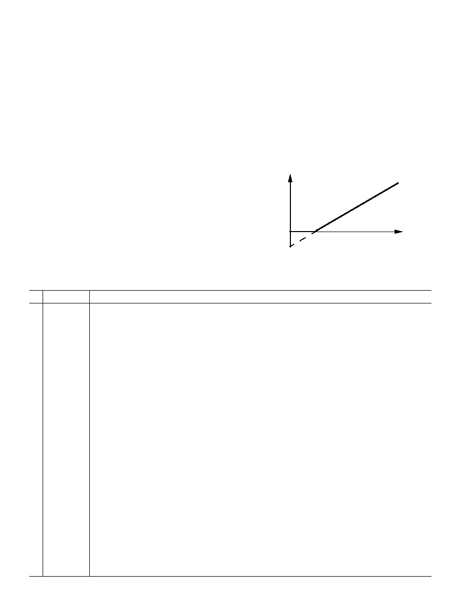
transfer function shown in Figure 1.
OUTPUT
VOLTAGE
NEGATIVE
OFFSET
DAC CODE
0V
{
Figure 1. Effect of Negative Offset (Single Supply)
REV. A
�5�
AD7243
TERMINOLOGY (Continued)
This "knee" is an offset effect, not a linearity error, and the
transfer function would have followed the dotted line if the out-
put voltage could have gone negative.
Normally, linearity is measured between zero (all 0s input code)
and full scale (all 1s input code) after offset and full scale have
been adjusted out or allowed for, but this is not possible in
single supply operation if the offset is negative, due to the knee
in the transfer function. Instead, linearity of the AD7243 in the
unipolar mode is measured between full scale and the lowest
code which is guaranteed to produce a positive output voltage.
This code is calculated from the maximum specification for
negative offset. For the A and B versions the linearity is mea-
sured between Codes 3 and 4095. For the S grade, linearity is
measured between Code 5 and Code 4095.
Differential Nonlinearity
Differential Nonlinearity is the difference between the measured
change and the ideal 1 LSB change between any two adjacent
codes. A specified differential nonlinearity of
�1 LSB or less
over the operating temperature range ensures monotonicity.
Unipolar Offset Error
Unipolar Offset Error is the measured output voltage from
V
OUT
with all zeros loaded into the DAC latch when the DAC is
configured for unipolar output. It is due to a combination of the
offset errors in the DAC and output amplifier.
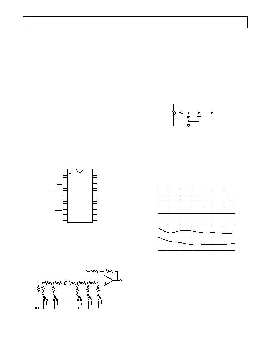
PIN CONFIGURATION
DIP and SOIC
TOP VIEW
(Not to Scale)
1
2
3
4
5
6
7
8
9
10
11
12
13
14
16
15
REFIN
REFOUT
CLR
BIN/COMP
SCLK
SDIN
SYNC
DGND
AGND
SDO
DCEN
LDAC
V
DD
V
SS
V
OUT
R
OFS
AD7243
CIRCUIT INFORMATION
D/A Section
The AD7243 contains a 12-bit voltage mode D/A converter
consisting of highly stable thin film resistors and high speed
NMOS single-pole, double-throw switches. The output voltage
from the converter has the same polarity as the reference volt-
age, REFIN, allowing single supply operation.
SHOWN FOR ALL 1S
ON DAC
*BUFFERED REFIN VOLTAGE
2R
2R
R
R
R
R
R
2R
2R
2R
2R
2R
2R
DB0
DB1
DB9
DB10
DB11
REFIN*
AGND
R
OFS
V
OUT
Figure 2. D/A Simplified Circuit Diagram
Internal Reference
The AD7243 has an on-chip temperature compensated buried
Zener reference which is factory trimmed to 5 V
� 50 mV. The
reference voltage is provided at the REFOUT pin. This refer-
ence can be used to provide the reference voltage for the D/A
converter (by connecting the REFOUT pin to the REFIN pin.)
The reference voltage can also be used as a reference for other
components and is capable of providing up to 500
�A to an ex-
ternal load. The maximum recommended capacitance on
REFOUT for normal operation is 50 pF. If the reference is re-
quired for external use with capacitive loads greater than 50 pF
then it should be decoupled to AGND with a 200
resistor in
series with a parallel combination of a 10
�F tantalum capacitor
and a 0.1
�F ceramic capacitor.
200
10 F
0.1 F
REFOUT
EXT
LOAD
Figure 3. Reference Decoupling Scheme
External Reference
In some applications, the user may require a system reference or
some other external reference to drive the AD7243. References
such as the AD586 provide an ideal external reference source
(see Figure 10). The REFIN voltage is internally buffered by a
unity gain amplifier before being applied to the D/A converter.
The D/A converter is scaled for a 5 V reference and the device is
tested with 5 V applied to REFIN. Other reference voltages may
be used with degraded performance. Figure 4 shows the typical
degradation in linearity vs. REFIN.
REFIN � Volts
1.0
2
LINEARITY ERROR � LSBs
0.9
0.8
0.7
0.6
0.5
0.4
0.3
0.2
0.1
0.0
3
4
5
6
7
8
9
V
DD
= +15V
V
SS
= �15V
T
A
= +25 C
INL
DNL
Figure 4. Typical Linearity vs. REFIN Voltage
Op Amp Section
The output of the voltage mode D/A converter is buffered by a
noninverting CMOS amplifier. The R
OFS
input allows three out-
put voltage ranges to be selected. The buffer amplifier is capable
of developing +10 V across a 2 k
load to AGND.
The output amplifier can be operated from a single +12 V to
+15 V supply by tying V
SS
= 0 V.
The amplifier can also be operated from dual supplies to allow
an additional bipolar output range of �5 V to +5 V. Dual supplies are
necessary for the bipolar output range but can also be used for
the unipolar ranges to give faster settling time to voltages near

AD7243
�6�
REV. A
0 V, to allow full sink capability of 2.5 mA over the entire
output range and to eliminate the effects of negative offsets on
the transfer characteristic (outlined previously). A plot of the
output sink capability of the amplifier is shown in Figure 5.
3
2
1
0
0
2
4
6
8
10
OUTPUT VOLTAGE � Volts
V = �15V
SS
V = 0V
SS
I
�
mA
SINK
Figure 5. Amplifier Sink Current
DIGITAL INTERFACE
The AD7243 contains an input serial to parallel shift register
and a DAC latch. A simplified diagram of the input loading
DAC LATCH (12 BITS)
INPUT SHIFT REGISTER (16 BITS)
GATING
SIGNAL
GATED
SCLK
SDO
RESET
EN
�
16
COUNTER/
DECODER
AUTO � UPDATE
CIRCUITRY
DCEN
SYNC
SCLK
SDIN
LDAC
CLR
Figure 6. Simplified Loading Structure
SCLK
DB11
MSB
DB14
*
DB13
*
DB12
*
DB0
LSB
*
= DON'T CARE
t
1
t
2
t
3
t
4
t
5
SDIN
SYNC
LDAC
CLR
DB15
*
t
6
t
7
t
8
t
9
Figure 7. Timing Diagram (Standalone Mode)
circuitry is shown in Figure 6. Serial data on the SDIN input is
loaded to the input register under control of DCEN,
SYNC and
SCLK. When a complete word is held in the shift register, it
may then be loaded into the DAC latch under control of
LDAC. Only the data in the DAC latch determines the analog
output on the AD7243.
The DCEN (daisy-chain enable) input is used to select either a
standalone mode or a daisy-chain mode. The loading format is
slightly different depending on which mode is selected.
Serial Data Loading Format (Standalone Mode)
With DCEN at Logic 0 the standalone mode is selected. In this
mode a low
SYNC input provides the frame synchronization
signal which tells the AD7243 that valid serial data on the SDIN
input will be available for the next 16 falling edges of SCLK. An
internal counter/decoder circuit provides a low gating signal so
that only 16 data bits are clocked into the input shift register.
After 16 SCLK pulses the internal gating signal goes inactive
(high) thus locking out any further clock pulses. Therefore, ei-
ther a continuous clock or a burst clock source may be used to
clock in the data.
The
SYNC input should be taken high after the complete 16-bit
word is loaded in.
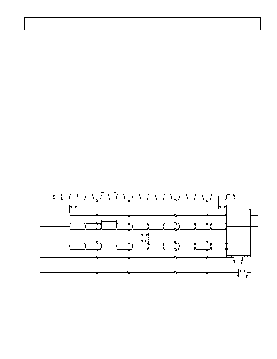
REV. A
�7�
AD7243
Although 16 bits of data are clocked into the input register, only
the latter 12 bits get transferred into the DAC latch. The first 4
bits in the 16 bit stream are don't cares since their value does
not affect the DAC latch data. Therefore, the data format is 4
don't cares followed by the 12-bit data word with the LSB as
the last bit in the serial stream.
There are two ways in which the DAC latch and hence the ana-
log output may be updated. The status of the
LDAC input is
examined after
SYNC is taken low. Depending on its status, one
of two update modes is selected.
If
LDAC = 0, then the automatic update mode is selected. In
this mode the DAC latch and analog output are updated auto-
matically when the last bit in the serial data stream is clocked in.
The update thus takes place on the sixteenth falling SCLK edge.
If
LDAC = 1, then the automatic update is disabled and the
DAC latch is updated by taking
LDAC low any time after the
16-bit data transfer is complete. The update now occurs on the
falling edge of
LDAC. Note that the LDAC input must be taken
back high again before the next data transfer is initiated.
Serial Data Loading Format (Daisy-Chain Mode)
By connecting DCEN high the daisy-chain mode is enabled.
This mode of operation is designed for multi-DAC systems
where several AD7243s may be connected in cascade (see Fig-
ure 16). In this mode the internal gating circuitry on SCLK is
disabled, and a serial data output facility is enabled. The inter-
nal gating signal is permanently active (low) so that the SCLK
signal is continuously applied to the input shift register when
SYNC is low. The data is clocked into the register on each fall-
ing SCLK edge after
SYNC going low. If more than 16 clock
pulses are applied, the data ripples out of the shift register and
appears on the SDO line. By connecting this line to the SDIN
input on the next AD7243 in the chain, a multi-DAC interface
may be constructed. Sixteen SCLK pulses are required for each
DAC in the system. Therefore, the total number of clock cycles
must equal 16N where N is the total number of devices in the
chain. When the serial transfer to all devices is complete,
SYNC
should be taken high. This prevents any further data being
clocked into the input register.
A continuous SCLK source may be used if it can be arranged
that
SYNC is held low for the correct number of clock cycles.
Alternatively, a burst clock containing the exact number of clock
cycles may be used and
SYNC taken high some time later.
When the transfer to all input registers is complete, a common
LDAC signal updates all DAC latches with the lower 12 bits of
data in each input register. All analog outputs are therefore up-
dated simultaneously on the falling edge of
LDAC.
Clear Function (
CLR)
The clear function bypasses the input shift register and loads the
DAC Latch with all 0s. It is activated by taking
CLR low. In all
ranges except the Offset Binary bipolar range (�5 V to +5 V) the
output voltage is reset to 0 V. In the offset binary bipolar range
the output is set to �REFIN. The clear function is especially
useful at power-up as it enables the output to be reset to a
known state.
SCLK
DB11 (N)
MSB
DB0 (N)
LSB
*
= DON'T CARE
SDIN
SYNC
LDAC
CLR
DB0 (N)
LSB
SDO
DB15 (N)*
DB15*
(N + 1)
DB11 (N + 1)
MSB
DB0 (N + 1)
LSB
UNDEFINED
DB15 (N)*
DB11 (N)
MSB
t
1
t
2
t
3
t
5
t
4
t
11
t
6
t
7
t
8
t
9
t
10
Figure 8. Timing Diagram (Daisy-Chain Mode)

AD7243
�8�
REV. A
APPLYING THE AD7243
Power Supply Decoupling
To achieve optimum performance when using the AD7243, the
V
DD
and V
SS
lines should each be decoupled to DGND using
0.1
�F capacitors. In noisy environments it is recommended
that 10
�F capacitors be connected in parallel with the 0.1 �F
capacitors.
The internal scaling resistors provided on the AD7243 allow
several output voltage ranges. The part can produce unipolar
output ranges of 0 V to +5 V or 0 V to +10 V and a bipolar out-
put range of
�5 V. Connections for the various ranges are out-
lined below.
Unipolar (0 V to +10 V) Configuration
The first of the configurations provides an output voltage range
of 0 V to +10 V. This is achieved by connecting the output off-
set resistor R
OFS
(Pin 13) to AGND. Natural Binary data format
is selected by connecting
BIN/COMP (Pin 4) to DGND. In this
configuration, the AD7243 can be operated using either single
or dual supplies. Note that the V
DD
supply must be
+14.25 V
for this range in order to maintain sufficient amplifier head-
room. Dual supplies may be used to improve settling time and
give increased current sink capability for the amplifier. Figure 9
shows the connection diagram for unipolar operation of the
AD7243. Table I shows the digital code vs. analog output for
this configuration.
DAC
AGND
DGND
REFOUT
REFIN
R
OFS
V
OUT
V
DD
2R
2R
AD7243*
BIN/
COMP
0V OR V
SS
0V TO + 10V
*ADDITIONAL PINS OMITTED FOR CLARITY
V
DD
V
SS
Figure 9. Unipolar (0 V to +10 V) Configuration
Table I. Unipolar Code Table (0 V to +10 V Range)
Input Data Word
MSB
LSB
Analog Output, V
OUT
XXXX 1111 1111 1111
+2 REFIN
� (4095/4096)
XXXX 1000 0000 0001
+2 REFIN
� (2049/4096)
XXXX 1000 0000 0000
+2 REFIN
� (2048/4096) = +REFIN
XXXX 0111 1111 1111
+2 REFIN
� (2047/4096)
XXXX 0000 0000 0001
+2 REFIN
� (1/4096)
XXXX 0000 0000 0000
0 V
X = Don't Care.
Note: 1 LSB = 2 REFIN/4096.
Unipolar (0 V to +5 V) Configuration
The 0 V to +5 V output voltage range is achieved by connecting
R
OFS
to V
OUT
. Once again, the AD7243 can be operated using
either single or dual supplies. The table for output voltage vs.
digital code is as in Table I, with 2REFIN replaced by REFIN.
Note, for this range, 1 LSB = REFIN � (2
�12
) = (REFIN/4096).
Bipolar ( 5 V) Configuration
The bipolar configuration for the AD7243, which gives an out-
put range of �5 V to +5 V, is achieved by connecting R
OFS
to
REFIN. The AD7243 must be operated from dual supplies to
achieve this output voltage range. Either offset binary or two's
complement data format may be selected. Figure 10 shows the
connection diagram for bipolar operation. An AD586 provides
the reference voltage for the DAC but this could be provided by
the on-chip reference by connecting REFOUT to REFIN.
V
DD
DAC
AGND
DGND
REFIN
R
OFS
2R
2R
AD7243*
BIN/ COMP
�5V TO + 5V
*ADDITIONAL PINS OMITTED FOR CLARITY
AD586
GND
+V
IN
V
OUT
V
DD
V
SS
V
SS
V
OUT
V
DD
Figure 10. Bipolar Configuration with External Reference
Bipolar Operation (Two's Complement Data Format)
The AD7243 is configured for two's complement data format
by connecting
BIN/COMP (Pin 4) high. The analog output vs.
digital code is shown in Table II.
Table II. Two's Complement Bipolar Code Table
Input Data Word
MSB
LSB
Analog Output, V
OUT
XXXX 0111 1111 1111
+REFIN
� (2047/2048)
XXXX 0000 0000 0001
+REFIN
� (1/2048)
XXXX 0000 0000 0000
0 V
XXXX 1111 1111 1111
�REFIN
� (1/2048)
XXXX 1000 0000 0001
�REFIN
� (2047/2048)
XXXX 1000 0000 0000
�REFIN
� (2048/2048) = �REFIN
X = Don't Care.
Note: 1 LSB = REFIN/2048.
Bipolar Operation (Offset Binary Data Format)
The AD7243 is configured for Offset Binary data format by
connecting
BIN/COMP (Pin 4) low. The analog output vs. digi-
tal code may be obtained by inverting the MSB in Table II.

REV. A
�9�
AD7243
MICROPROCESSOR INTERFACING
Microprocessor interfacing to the AD7243 is via a serial bus
which uses standard protocol compatible with DSP processors
and microcontrollers. The communications channel requires a
three-wire interface consisting of a clock signal, a data signal
and a synchronization signal. The AD7243 requires a 16-bit
data word with data valid on the falling edge of SCLK. For all
the interfaces, the DAC update may be done automatically
when all the data is clocked in or it may be done under control
of
LDAC.
Figures 11 to 16 show the AD7243 configured for interfacing to
a number of popular DSP processors and microcontrollers.
AD7243�ADSP-2101/ADSP-2102 Interface
Figure 11 shows a serial interface between the AD7243 and the
ADSP-2101/ADSP-2102 DSP processor. The ADSP-2101/
ADSP-2102 contains two serial ports, and either port may be
used in the interface. The data transfer is initiated by
TFS going
low. Data from the ADSP-2101/ADSP-2102 is clocked into the
AD7243 on the falling edge of SCLK. When the data transfer is
complete,
TFS is taken high. In the interface shown the DAC is
updated using an external timer which generates an
LDAC
pulse. This could also be done using a control or decoded ad-
dress line from the processor. Alternatively, the
LDAC input
could be hard wired low and in this case the update takes place
automatically on the sixteenth falling edge of SCLK.
ADSP - 2101/
ADSP - 2102*
TIMER
TFS
SCLK
DT
LDAC
SYNC
SCLK
SDIN
AD7243*
*ADDITIONAL PINS OMITTED FOR CLARITY
Figure 11. AD7243�ADSP-2101/ADSP-2102 Interface
AD7243�DSP56000 Interface
A serial interface between the AD7243 and the DSP56000 is
shown in Figure 12. The DSP56000 is configured for Normal
Mode Asynchronous operation with Gated Clock. It is also set
up for a 16-bit word with SCK and SC2 as outputs and the FSL
control bit set to a "0." SCK is internally generated on the
DSP56000 and applied to the AD7243 SCLK input. Data from
the DSP56000 is valid on the falling edge of SCK. The SC2
output provides the framing pulse for valid data. This line must
be inverted before being applied to the
SYNC input of the
AD7243.
The
LDAC input of the AD7243 is connected to DGND so the
update of the DAC latch takes place automatically on the six-
teenth falling edge of SCLK. An external timer could also be
used as in the previous interface if an external update is
required.
DSP56000
SCK
STD
SC2
LDAC
SCLK
SDIN
AD7243*
SYNC
*ADDITIONAL PINS OMITTED FOR CLARITY
Figure 12. AD7243�DSP56000 Interface
AD7243�TMS32020 Interface
Figure 13 shows a serial interface between the AD7243 and the
TMS32020 DSP processor. In this interface, the CLKX and
FSX signals for the TMS32020 should be generated using ex-
ternal clock/timer circuitry. The FSX pin of the TMS32020
must be configured as an input. Data from the TMS32020 is
valid on the falling edge of CLKX.
The clock/timer circuitry generates the
LDAC signal for the
AD7243 to synchronize the update of the output with the serial
transmission. Alternatively, the automatic update mode may be
selected by connecting
LDAC to DGND.
LDAC
SYNC
SCLK
SDIN
AD7243*
*ADDITIONAL PINS OMITTED FOR CLARITY
CLOCK/
TIMER
TMS32020
FSX
CLKX
DX
Figure 13. AD7243�TMS32020 Interface
AD7243
�10�
REV. A
AD7243�87C51 Interface
A serial interface between the AD7243 and the 87C51
microcontroller is shown in Figure 14. TXD of the 87C51 drives
SCLK of the AD7243, while RXD drives the serial data line of
the part. The
SYNC signal is derived from the port line P3.3.
The 87C51 provides the LSB of its SBUF register as the first bit
in the serial data stream. Therefore, the user will have to ensure
that the data in the SBUF register is arranged correctly so that
the don't care bits are the first to be transmitted to the AD7243
and the last bit to be sent is the LSB of the word to be loaded to
the AD7243. When data is to be transmitted to the part, P3.3 is
taken low. Data on RXD is valid on the falling edge of TXD.
The 87C51 transmits its serial data in 8-bit bytes with only eight
falling clock edges occurring in the transmit cycle. To load data
to the AD7243, P3.3 is left low after the first eight bits are trans-
ferred and a second byte of data is then transferred serially to the
AD7243. When the second serial transfer is complete, the P3.3
line is taken high.
Figure 14 shows the
LDAC input of the AD7243 hard wired
low. As a result, the DAC latch and the analog output will be up-
dated on the sixteenth falling edge of TXD after the
SYNC sig-
nal for the DAC has gone low. Alternatively, the scheme used in
previous interfaces, whereby the
LDAC input is driven from a
timer, can be used.
LDAC
SCLK
SDIN
AD7243*
SYNC
*ADDITIONAL PINS OMITTED FOR CLARITY
P3.3
TXD
RXD
87C51*
Figure 14. AD7243�87C51 Interface
AD7243�68HC11 Interface
Figure 15 shows a serial interface between the AD7243 and the
68HC11 microcontroller. SCK of the 68HC11 drives SCLK of
the AD7243 while the MOSI output drives the serial data line of
the AD7243. The
SYNC signal is derived from a port line (PC7
shown).
For correct operation of this interface, the 68HC11 should be
configured such that its CPOL bit is a 0 and its CPHA bit is a 1.
When data is to be transmitted to the part, PC7 is taken low.
When the 68HC11 is configured like this, data on MOSI is valid
on the falling edge of SCK. The 68HC11 transmits its serial data
in 8-bit bytes with only eight falling clock edges occurring in the
transmit cycle. To load data to the AD7243, PC7 is left low after
the first eight bits are transferred and a second byte of data is
then transferred serially to the AD7243. When the second serial
transfer is complete, the PC7 line is taken high.
Figure 15 shows the
LDAC input of the AD7243 hardwired
low. As a result, the DAC latch and the analog output of the
DAC will be updated on the sixteenth falling edge of SCK after
the respective
SYNC signal has gone low. Alternatively, the
scheme used in previous interfaces, whereby the
LDAC input is
driven from a timer, can be used.
LDAC
SCLK
SDIN
AD7243*
SYNC
*ADDITIONAL PINS OMITTED FOR CLARITY
PC7
SCK
MOSI
68HC11*
Figure 15. AD7243�68HC11 Interface
Multiple DAC Daisy-Chain Interface
A multi-DAC serial interface is shown in Figure 16. This
scheme may be used with all of the interfaces previously dis-
cussed if more than one DAC is required in a system. To enable
the facility the DCEN pin must be connected high on all de-
vices, including the last device in the chain.
SCLK
AD7243*
SYNC
LDAC
*ADDITIONAL PINS OMITTED FOR CLARITY
PA1
PA2
PA3
MICROCONTROLLER
PA0
SDIN
DCEN
SDO
SCLK
AD7243*
SYNC
LDAC
SDIN
DCEN
SDO
SCLK
AD7243*
SYNC
LDAC
SDIN
DCEN
SDO
V
DD
V
DD
V
DD
Figure 16. AD7243 Daisy-Chain Configuration
REV. A
�11�
AD7243
Common clock, data, and synchronization signals are applied to
all DACs in the chain. The loading sequence starts by taking
SYNC low. The data is then clocked into the input registers on
the falling edge of SCLK. Sixteen clock pulses are required for
each DAC in the chain. The data ripples through the input reg-
isters with the first 16-bit word filling the last register in the
chain after 16N clock pulses where N = the total number of
DACs in the chain.
When valid data has been loaded into all the registers, the
SYNC input should be taken high and a common LDAC pulse
used to update all the DACs simultaneously.
APPLICATIONS
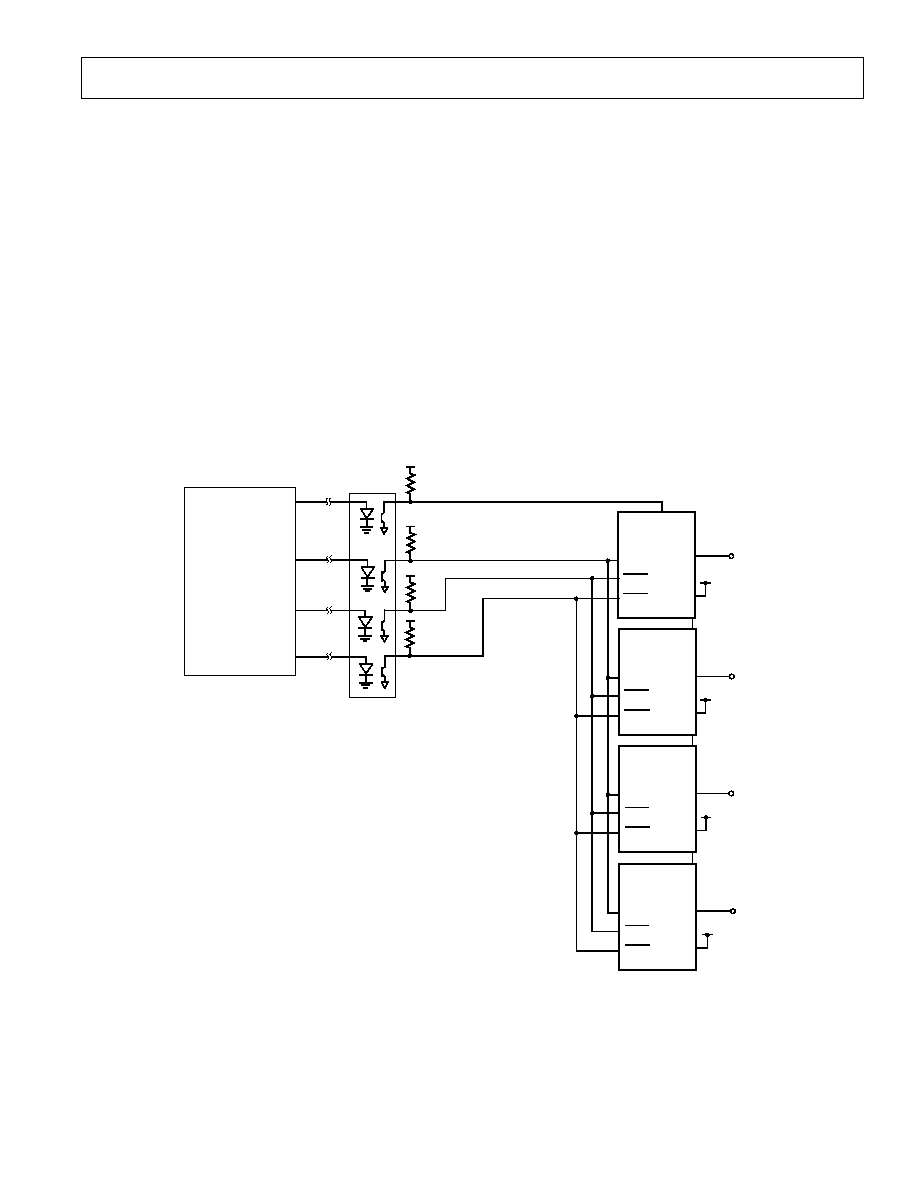
OPTO-ISOLATED INTERFACE
In many process control type applications it is necessary to pro-
vide an isolation barrier between the controller and the unit be-
ing controlled. Opto-isolators can provide voltage isolation in
excess of 3 kV. The serial loading structure of the AD7243
makes it ideal for opto-isolated interfaces as the number of in-
terface lines is kept to a minimum.
Figure 17 shows a 4-channel isolated interface using the
AD7243. The DCEN pin must be connected high to enable the
daisy-chain facility. Four channels with 12-bit resolution are
provided in the circuit shown, but this may be expanded to ac-
commodate any number of DAC channels without any extra
isolation circuitry.
The sequence of events to program the output channels is as
follows:
1. Take the
SYNC line low.
2. Transmit the data as four 16-bit words. A total of 64 clock
pulses is required to clock the data through the chain.
3. Take the
SYNC line high.
4. Pulse the
LDAC line low. This updates all output channels
simultaneously on the falling edge of
LDAC.
To reduce the number of opto-couplers, the
LDAC line could
be driven from a one shot which is triggered by the rising edge
on the
SYNC line. A low level pulse of 50 ns duration or greater
is all that is required to update the outputs.
SCLK
AD7243*
SYNC
LDAC
SDIN
DCEN
SDO
SCLK
AD7243*
SYNC
LDAC
SDIN
DCEN
SDO
SCLK
AD7243*
SYNC
LDAC
SDIN
DCEN
SDO
SCLK
AD7243*
SYNC
LDAC
SDIN
DCEN
SDO
V
OUT
*ADDITIONAL PINS OMITTED FOR CLARITY
DATA OUT
CLOCK OUT
SYNC OUT
CONTROL OUT
CONTROLLER
V
DD
V
OUT
(A)
QUAD OPTO-COUPLER
V
DD
V
DD
V
DD
V
DD
V
DD
V
DD
V
DD
V
OUT
(B)
V
OUT
(C)
V
OUT
(D)
V
OUT
V
OUT
V
OUT
Figure 17. Four-Channel Opto-lsolated Interface

AD7243
�12�
REV. A
OUTLINE DIMENSIONS
Dimensions shown in inches and (mm).
C1498a�1�6/00 (rev. A) 00993
PRINTED IN U.S.A.
Plastic DIP (N-16)
0.125
(3.18)
MIN
0.035
(0.89)
0.18
(4.57)
0.3 (7.62)
0.87 (22.1) MAX
0.25
(6.35)
0.31
(7.87)
0.18
(4.57)
MAX
0.011
(0.28)
1
8
9
16
0.018 (0.46)
0.033 (0.84)
0.1 (2.54)
Cerdip (Q-16)
0.310 (7.87)
0.220 (5.59)
16
1
9
8
TOP VIEW
(Not to Scale)
0.320 (8.13)
0.290 (7.37)
0.015 (0.381)
0.008 (0.204)
0.200
(5.08)
MAX
0.100 BSC
(2.54 BSC)
0.840 (21.34) MAX
0.060 (1.52)
0.015 (0.38)
0.150 (3.81) MIN
0.070 (1.78)
0.30 (0.76)
0.022 (0.558)
0.014 (0.356)
SOIC (R-16)
1
8
9
16
0.413 (10.49)
0.398 (10.11)
0.419 (10.64)
0.394 (10.01)
0.300 (7.62)
0.292 (7.42)
0.350 (8.89)
0.011 (0.279)
0.004 (0.102)
STANDOFF
0.050 (1.27) REF
0.019 (0.483)
0.014 (0.356)
0.104 (2.64)
0.093 (2.36)
0.02 (0.508)
45 C
CHAMP
o
0.01 (0.254)
0.050 (1.27)