AD813
REV. B
a
Information furnished by Analog Devices is believed to be accurate and
reliable. However, no responsibility is assumed by Analog Devices for its
use, nor for any infringements of patents or other rights of third parties
which may result from its use. No license is granted by implication or
otherwise under any patent or patent rights of Analog Devices.
Single Supply, Low Power
Triple Video Amplifier
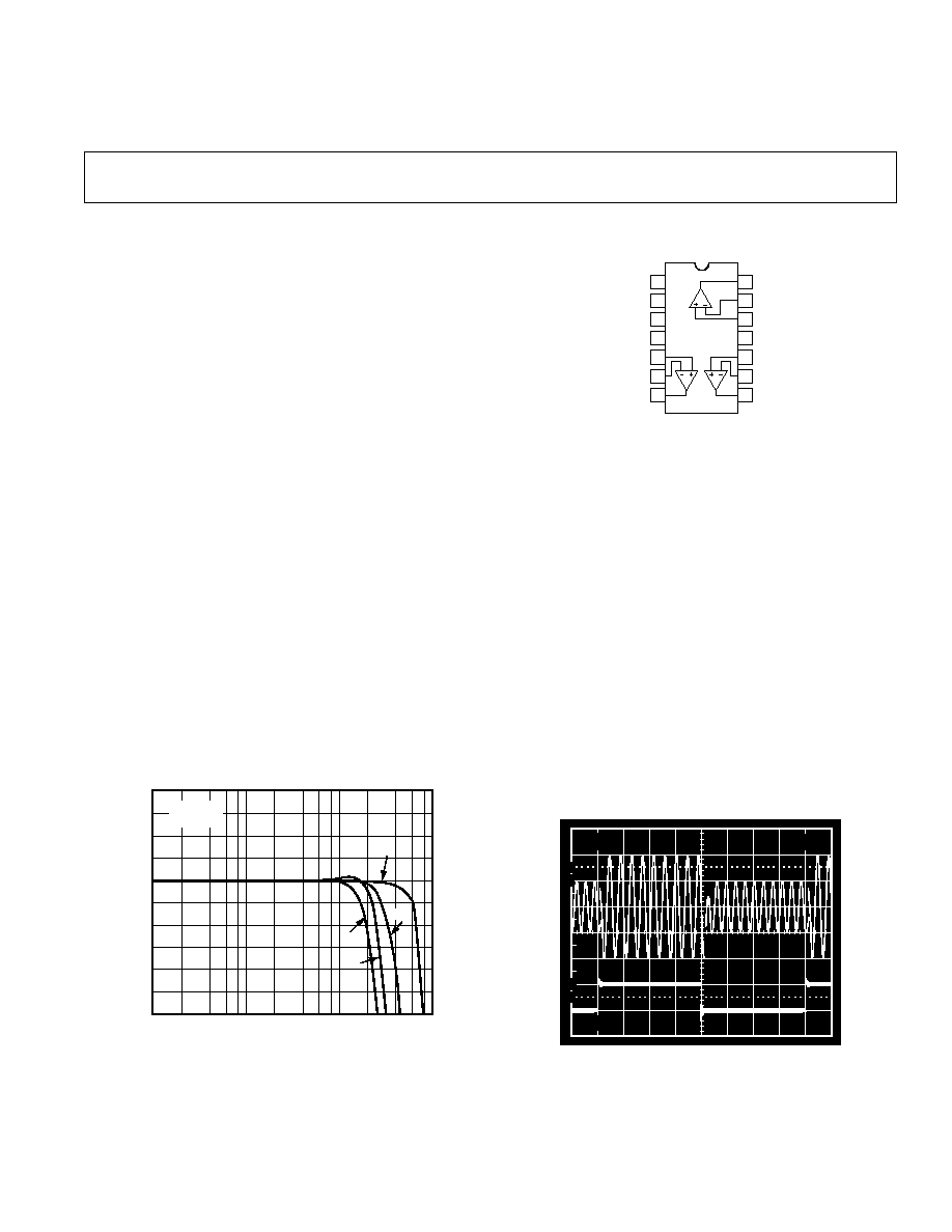
PIN CONFIGURATION
14-Lead DIP and SOIC
DISABLE1
DISABLE2
OUT2
≠IN2
+IN1
≠IN1
OUT1
DISABLE3
V
S
+
+IN2
V
S
≠
1
2
14
13
5
6
7
10
9
8
3
4
12
11
AD813
+IN3
≠IN3
OUT3
FEATURES
Low Cost
Three Video Amplifiers in One Package
Optimized for Driving Cables in Video Systems
Excellent Video Specifications (R
L
= 150 )
Gain Flatness 0.1 dB to 50 MHz
0.03% Differential Gain Error
0.06 Differential Phase Error
Low Power
Operates on Single +3 V to 15 V Power Supplies
5.5 mA/Amplifier Max Power Supply Current
High Speed
125 MHz Unity Gain Bandwidth (≠3 dB)
500 V/ s Slew Rate
High Speed Disable Function per Channel
Turn-Off Time 80 ns
Easy to Use
50 mA Output Current
Output Swing to 1 V of Rails
APPLICATIONS
Video Line Driver
LCD Drivers
Computer Video Plug-In Boards
Ultrasound
RGB Amplifier
CCD Based Systems
50 MHz while offering differential gain and phase error of
0.03% and 0.06
∞
. This makes the AD813 ideal for broadcast
and consumer video electronics.
The AD813 offers low power of 5.5 mA per amplifier max and
runs on a single +3 V power supply. The outputs of each ampli-
fier swing to within one volt of either supply rail to easily accom-
modate video signals. While operating on a single +5 V supply
the AD813 still achieves 0.1 dB flatness to 20 MHz and 0.05%
& 0.05
∞
of differential gain and phase performance. All this is
offered in a small 14-lead plastic DIP or SOIC package. These
features make this triple amplifier ideal for portable and battery
powered applications where size and power are critical.
The outstanding bandwidth of 125 MHz along with 500 V/
µ
s of
slew rate make the AD813 useful in many general purpose, high
speed applications where a single +3 V or dual power supplies
up to
±
15 V are needed. Furthermore the AD813 contains a
high speed disable function for each amplifier in order to power
down the amplifier or high impedance the output. This can then
be used in video multiplexing applications. The AD813 is avail-
able in the industrial temperature range of ≠40
∞
C to +85
∞
C in
plastic DIP and SOIC packages as well as chips.
PRODUCT DESCRIPTION
The AD813 is a low power, single supply triple video amplifier.
Each of the three current feedback amplifiers has 50 mA of output
current, and is optimized for driving one back-terminated video
load (150
). The AD813 features gain flatness of 0.1 dB to
10
90
100
0%
5V
500mV
500ns
Figure 2. Channel Switching Characteristics for a 3:1 Mux
100k
1M
100M
10M
FREQUENCY ≠ Hz
0
0.2
0.1
≠0.1
≠0.2
≠0.3
≠0.4
NORMALIZED GAIN ≠ dB
≠0.5
3V
15V
5V
G = +2
R
L
= 150
5V
Figure 1. Fine Scale Gain Flatness vs. Frequency,
G = +2, R
L
= 150
One Technology Way, P.O. Box 9106, Norwood, MA 02062-9106, U.S.A.
Tel: 781/329-4700
World Wide Web Site: http://www.analog.com
Fax: 781/326-8703
© Analog Devices, Inc., 1998
ORDERING GUIDE
Temperature
Package
Package
Model
Range
Description
Options
AD813AN
≠40
∞
C to +85
∞
C
14-Lead Plastic DIP
N-14
AD813AR-14
≠40
∞
C to +85
∞
C
14-Lead Plastic SOIC
R-14
AD813ACHIPS
≠40
∞
C to +85
∞
C
Die Form
AD813AR-REEL
13" REEL
AD813AR-REEL7
7" REEL
5962-9559601M2A*
≠55
∞
C to +125
∞
C
20-Lead LCC
*Refer to official DSCC drawing for tested specifications and pin configuration.
ABSOLUTE MAXIMUM RATINGS
1
Supply Voltage . . . . . . . . . . . . . . . . . . . . . . . . . . . . . . . .
±
18 V
Internal Power Dissipation
2
Plastic (N) . . . . . . . . . . . . . . . . . . . . . . . . . . . . . . 1.6 Watts
Small Outline (R) . . . . . . . . . . . . . . . . . . . . . . . . . 1.0 Watts
Input Voltage (Common Mode) . . . . . . . . . . . . . . . . . . .
±
V
S
Differential Input Voltage . . . . . . . . . . . . . . . . . . . . . . . .
±
6 V
Output Short Circuit Duration
. . . . . . . . . . . . . . . . . . . . . . . Observe Power Derating Curves
Storage Temperature Range N, R . . . . . . . . ≠65
∞
C to +125
∞
C
Operating Temperature Range
AD813A . . . . . . . . . . . . . . . . . . . . . . . . . . . ≠40
∞
C to +85
∞
C
Lead Temperature Range (Soldering 10 sec) . . . . . . . +300
∞
C
NOTES
1
Stresses above those listed under Absolute Maximum Ratings may cause perma-
nent damage to the device. This is a stress rating only; functional operation of the
device at these or any other conditions above those indicated in the operational
section of this specification is not implied. Exposure to absolute maximum rating
conditions for extended periods may affect device reliability.
2
Specification is for device in free air:
14-Lead Plastic DIP Package:
JA
= 75
∞
C/W
14-Lead SOIC Package:
JA
= 120
∞
C/W
AD813
Model
AD813A
Conditions
V
S
Min
Typ
Max
Units
MATCHING CHARACTERISTICS
Dynamic
Crosstalk
G = +2, f = 5 MHz
+5 V, +3 V
≠65
dB
Gain Flatness Match
G = +2, f = 20 MHz
+5 V, +3 V
0.1
dB
DC
Input Offset Voltage
T
MIN
≠T
MAX
+5 V, +3 V
0.5
3.5
mV
≠Input Bias Current
T
MIN
≠T
MAX
+5 V, +3 V
2
25
µ
A
POWER SUPPLY
Operating Range
2.4
36
V
Quiescent Current
Per Amplifier
+5 V
3.2
4.0
mA
+3 V
3.0
4.0
mA
T
MIN
≠T
MAX
+5 V
5.0
mA
Quiescent Current, Powered Down
Per Amplifier
+5 V
0.4
0.6
mA
+3 V
0.4
0.5
mA
Power Supply Rejection Ratio
Input Offset Voltage
V
S
= +3.0 V to +30 V
76
dB
≠Input Current
0.3
µ
A/V
+Input Current
0.005
µ
A/V
DISABLE CHARACTERISTICS
Off Isolation
f = 5 MHz
+5 V, +3 V
≠55
dB
Off Output Impedance
G = +1
+5 V, +3 V
13
pF
Channel-to-Channel
2 or 3 Channel
+5 V, +3 V
≠65
dB
Isolation
Mux, f = 5 MHz
Turn-On Time
+5 V, +3 V
100
ns
Turn-Off Time
80
ns
TRANSISTOR COUNT
111
NOTES
1
Slew rate measurement is based on 10% to 90% rise time in the specified closed-loop gain.
2
Single supply differential gain and phase are measured with the ac coupled circuit of Figure 52.
Specifications subject to change without notice.
≠5≠
REV. B