Document Outline
- FEATURES
- APPLICATIONS
- GENERAL DESCRIPTION
- FUNCTIONAL BLOCK DIAGRAMS
- PRODUCT HIGHLIGHTS
- ˛ˇ
- ˛ˇ
- ˛ˇ
- ˛ˇ
- ˛ˇ
- ˛ˇ

<0.5 CMOS 1.65 V to 3.6 V
Quad SPST Switches
ADG811/ADG812/ADG813
Rev. A
Information furnished by Analog Devices is believed to be accurate and reliable.
However, no responsibility is assumed by Analog Devices for its use, nor for any
infringements of patents or other rights of third parties that may result from its use.
Specifications subject to change without notice. No license is granted by implication
or otherwise under any patent or patent rights of Analog Devices. Trademarks and
registered trademarks are the property of their respective owners.
One Technology Way, P.O. Box 9106, Norwood, MA 02062-9106, U.S.A.
Tel: 781.329.4700
www.analog.com
Fax: 781.326.8703
© 2004 Analog Devices, Inc. All rights reserved.
FEATURES
0.5 typ on resistance
0.8 max on resistance at 125∞C
1.65 V to 3.6 V operation
Automotive temperature range: ≠40∞C to +125∞C
High current carrying capability: 300 mA continuous
Rail-to-rail switching operation
Fast switching times: <25 ns
Typical power consumption < 0.1 µW
APPLICATIONS
Cellular phones
MP3 players
Power routing
Battery-powered systems
PCMCIA cards
Modems
Audio and video signal routing
Communications systems
FUNCTIONAL BLOCK DIAGRAMS
S1
D1
S2
D2
S3
D3
S4
D4
IN1
IN2
IN3
IN4
ADG811
SWITCHES SHOWN FOR A LOGIC 1 INPUT
S1
D1
S2
D2
S3
D3
S4
D4
IN1
IN2
IN3
IN4
ADG812
S1
D1
S2
D2
S3
D3
S4
D4
IN1
IN2
IN3
IN4
ADG813
04306-A
-
001
Figure 1.
GENERAL DESCRIPTION
The ADG811, ADG812, and ADG813 are low voltage CMOS
devices containing four independently selectable switches.
These switches offer ultralow on resistance of less than 0.8
over the full temperature range. The digital inputs can handle
1.8 V logic with a 2.7 V to 3.6 V supply.
These devices contain four independent single-pole/single-
throw (SPST) switches. The ADG811 and ADG812 differ only
in that the digital control logic is inverted. The ADG811
switches are turned on with a logic low on the appropriate
control input, while a logic high is required to turn on the
switches of the ADG812. The ADG813 contains two switches
whose digital control logic is similar to the ADG811, while the
logic is inverted on the other two switches.
Each switch conducts equally well in both directions when on
and has an input signal range that extends to the supplies. The
ADG813 exhibits break-before-make switching action.
The ADG811, ADG812, and ADG813 are fully specified for
3.3 V, 2.5 V, and 1.8 V supply operation. They are available in a
16-lead TSSOP package.
PRODUCT HIGHLIGHTS
1.
<0.8 over full temperature range of ≠40∞C to +125∞C.
2.
Single 1.65 V to 3.6 V operation.
3.
Operational with 1.8 V CMOS logic.
4.
High current handling capability (300 mA continuous
current at 3.3 V).
5.
Low THD+N (0.02% typ).

ADG811/ADG812/ADG813
Rev. A | Page 2 of 16
TABLE OF CONTENTS
ADG811/ADG812/ADG813--Specifications .............................. 3
Absolute Maximum Ratings............................................................ 6
ESD Caution.................................................................................. 6
Pin Configuration and Function Descriptions............................. 7
Typical Performance Characteristics ..............................................8
Test Circuits..................................................................................... 11
Outline Dimensions ....................................................................... 13
Ordering Guide .......................................................................... 13
REVISION HISTORY
5/04--Data Sheet Changed from Rev. 0 to Rev. A
Updated Format..............................................................Universal
Updated Package Choices..............................................Universal
11/03--Revision 0: Initial Version

ADG811/ADG812/ADG813
Rev. A | Page 3 of 16
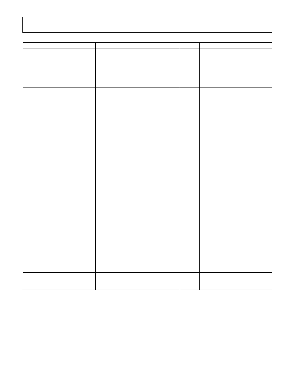
ADG811/ADG812/ADG813--SPECIFICATIONS
Table 1. V
DD
= 2.7 V to 3.6 V, GND = 0 V, unless otherwise noted
1
Parameter
+25∞C
≠40∞C to +85∞C
≠40∞C to +125∞C
Unit
Test Conditions/Comments
ANALOG SWITCH
Analog Signal Range
0 V to V
DD
V
On Resistance (R
ON
) 0.5
typ
V
DD
= 2.7 V, V
S
= 0 V to V
DD
, I
S
= 10 mA;
0.65
0.75
0.8
max
Figure 18
0.04
typ V
DD
= 2.7 V, V
S
= 0.5 V, I
S
= 10 mA
On Resistance Match between
Channels (R
ON
)
0.075
0.08
max
On Resistance Flatness (R
FLAT(ON)
) 0.1
typ
V
DD
= 2.7 V, V
S
= 0 V to V
DD
, I
S
= 10 mA
0.15
0.16
max
LEAKAGE CURRENTS
V
DD
= 3.6 V
Source Off Leakage I
S
(OFF)
±0.2
nA typ
V
S
= 0.6 V/3.3 V, V
D
= 3.3 V/0.6 V;
±1
±8
±80
nA max
Figure 19
Drain Off Leakage I
D
(OFF)
±0.2
nA typ
V
S
= 0.6 V/3.3 V, V
D
= 3.3 V/0.6 V;
±1
±8
±80
nA max
Figure 19
Channel On Leakage I
D
, I
S
(ON)
±0.2
nA typ
V
S
= V
D
= 0.6 V or 3.3 V; Figure 20
±1
±15
±90
nA
max
DIGITAL INPUTS
Input High Voltage, V
INH
2
V
min
Input Low Voltage, V
INL
0.8 V
max
Input Current, I
INL
or I
INH
0.005
µA
typ
V
IN
= V
INL
or V
INH
±0.1
µA
max
C
IN
, Digital Input Capacitance
6
pF typ
DYNAMIC CHARACTERISTICS
2
t
ON
21
ns
typ
R
L
= 50 , C
L
= 35 pF
25
26
28
ns
max
V
S
= 1.5 V/0 V; Figure 21
t
OFF
4
ns
typ
R
L
= 50 , C
L
= 35 pF
5
6
7
ns
max
V
S
= 1.5 V; Figure 21
Break-Before-Make Time Delay (t
BBM
) 17
ns
typ R
L
= 50 , C
L
= 35 pF
(ADG813 only)
5
ns min
V
S1
= V
S2
= 1.5 V; Figure 22
Charge Injection
30
pC typ
V
S
= 1.5 V, R
S
= 0 , C
L
= 1 nF;
Figure 23
Off Isolation
≠67
dB typ
R
L
= 50 , C
L
= 5 pF, f = 100 kHz;
Figure 24
Channel-to-Channel Crosstalk
≠90
dB typ
R
L
= 50 , C
L
= 5 pF, f = 100 kHz;
Figure 26
Total Harmonic Distortion (THD + N)
0.02
%
R
L
= 32 , f = 20 Hz to 20 kHz,
V
S
= 2 V p-p
Insertion Loss
≠0.05
dB typ
R
L
= 50 , C
L
= 5 pF, f = 100 kHz
≠3 dB Bandwidth
90
MHz typ
R
L
= 50 , C
L
= 5 pF; Figure 25
C
S
(OFF)
30
pF typ
C
D
(OFF)
35
pF typ
C
D
, C
S
(ON)
60
pF typ
POWER REQUIREMENTS
V
DD
= 3.6 V
I
DD
0.003
µA typ
Digital inputs = 0 V or 3.6 V
1.0
4
µA
max
1
Temperature range for the Y version is ≠40∞C to +125∞C.
2
Guaranteed by design, not subject to production test.
ADG811/ADG812/ADG813
Rev. A | Page 4 of 16
Table 2. V
DD
= 2.5 V ± 0.2 V, GND = 0 V, unless otherwise noted
1
Parameter
+25∞C
≠40∞C to +85∞C
≠40∞C to +125∞C
Unit
Test Conditions/Comments
ANALOG SWITCH
Analog Signal Range
0 V to V
DD
V
On Resistance (R
ON
) 0.65
typ
V
DD
= 2.3 V, V
S
= 0 V to V
DD
, I
S
= 10 mA;
0.72
0.8
0.88
max
Figure 18
0.04
typ V
DD
= 2.3 V; V
S
= 0.55 V, I
S
= 10 mA
On Resistance Match between
Channels (R
ON
)
0.08
0.085
max
On Resistance Flatness (R
FLAT(ON)
) 0.16
typ
V
DD
= 2.3 V; V
S
= 0 V to V
DD
, I
S
= 10 mA
0.23
0.24
max
LEAKAGE CURRENTS
V
DD
= 2.7 V
Source Off Leakage I
S
(OFF)
±0.2
nA typ
V
S
= 0.6 V/2.4 V, V
D
= 2.4 V/0.6 V;
±1
±6
±35
nA max
Figure 19
Drain Off Leakage I
D
(OFF)
±0.2
nA typ
V
S
= 0.6 V/2.4 V, V
D
= 2.4 V/0.6 V;
±1
±6
±35
nA max
Figure 19
Channel On Leakage I
D
, I
S
(ON)
±0.2
nA typ
V
S
= V
D
= 0.6 V or 2.4 V; Figure 20
±1
±11
±70
nA
max
DIGITAL INPUTS
Input High Voltage, V
INH
1.7 V
min
Input Low Voltage, V
INL
0.7 V
max
Input Current, I
INL
or I
INH
0.005
µA
typ
V
IN
= V
INL
or V
INH
±0.1
µA
max
C
IN
, Digital Input Capacitance
6
pF typ
DYNAMIC CHARACTERISTICS
2
t
ON
22
ns
typ
R
L
= 50 , C
L
= 35 pF
27
29
30
ns
max
V
S
= 1.5 V/ 0 V; Figure 21
t
OFF
4
ns
typ
R
L
= 50 , C
L
= 35 pF
6
7
8
ns
max
V
S
= 1.5 V; Figure 21
Break-Before-Make Time Delay (t
BBM
) 18
ns
typ R
L
= 50 , C
L
= 35 pF
(ADG813 only)
5
ns min
V
S1
= V
S2
= 1.5 V; Figure 22
Charge Injection
25
pC typ
V
S
= 1.25 V, R
S
= 0 , C
L
= 1 nF;
Figure 23
Off Isolation
≠67
dB typ
R
L
= 50 , C
L
= 5 pF, f = 100 kHz;
Figure 24
Channel-to-Channel Crosstalk
≠90
dB typ
R
L
= 50 , C
L
= 5 pF, f = 100 kHz;
Figure 26
Total Harmonic Distortion (THD + N)
0.022
%
R
L
= 32 , f = 20 Hz to 20 kHz,
V
S
= 1.5 V p-p
Insertion Loss
≠0.06
dB typ
R
L
= 50 , C
L
= 5 pF, f = 100 kHz
≠3 dB Bandwidth
90
MHz typ
R
L
= 50 , C
L
= 5 pF; Figure 25
C
S
(OFF)
32
pF typ
C
D
(OFF)
37
pF typ
C
D
, C
S
(ON)
60
pF typ
POWER REQUIREMENTS
V
DD
= 2.7 V
I
DD
0.003
µA typ
Digital inputs = 0 V or 2.7 V
1.0
4
µA
max
1
Temperature range for the Y version is ≠40∞C to +125∞C.
2
Guaranteed by design, not subject to production test.
ADG811/ADG812/ADG813
Rev. A | Page 5 of 16
Table 3. V
DD
= 1.65 V to 1.95 V, GND = 0 V, unless otherwise noted
1
Parameter
+25∞C ≠40∞C
to
+85∞C ≠40∞C
to +125∞C
Unit
Test Conditions/Comments
ANALOG SWITCH
Analog Signal Range
0 V to V
DD
V
On Resistance (R
ON
) 1
typ
V
DD
= 1.8 V, V
S
= 0 V to V
DD
, I
S
= 10 mA;
1.4
2.2
2.2
max
Figure 18
2.5
4
4
max
V
DD
= 1.65 V, V
S
= 0 V to V
DD
, I
S
= 10 mA
On Resistance Match between
Channels (R
ON
)
0.1
typ V
DD
= 1.65 V, V
S
= 0.7 V, I
S
= 10 mA
LEAKAGE CURRENTS
V
DD
= 1.95 V
Source Off Leakage I
S
(OFF)
±0.2
nA typ
V
S
= 0.6 V/1.65 V, V
D
= 1.65 V/0.6 V;
±1
±5
±30
nA max
Figure 19
Drain Off Leakage I
D
(OFF)
±0.2
nA typ
V
S
= 0.6 V/1.65 V, V
D
= 1.65 V/0.6 V;
±1
±5
±30
nA max
Figure 19
Channel On Leakage I
D
, I
S
(ON)
±0.2
nA typ
V
S
= V
D
= 0.6 V or 1.65 V; Figure 20
±1
±9
±60
nA
max
DIGITAL INPUTS
Input High Voltage, V
INH
0.65V
DD
V
min
Input Low Voltage, V
INL
0.35V
DD
V
max
Input Current, I
INL
or I
INH
0.005
µA
typ
V
IN
= V
INL
or V
INH
±0.1
µA
max
CIN, Digital Input Capacitance
6
pF typ
DYNAMIC CHARACTERISTICS
2
t
ON
27
ns
typ
R
L
= 50 , C
L
= 35 pF
35
36
37
ns
max
V
S
= 1.5 V/ 0 V; Figure 21
t
OFF
6
ns typ
R
L
= 50 , C
L
= 35 pF
8
9
10
ns
max
V
S
= 1.5 V; Figure 21
Break-Before-Make Time Delay (t
BBM
) 20
ns
typ R
L
= 50 , C
L
= 35 pF
(ADG813 only)
5
ns min
V
S1
= V
S2
= 1 V; Figure 22
Charge Injection
15
pC typ
V
S
= 1 V, R
S
= 0 , C
L
= 1 nF;
Figure 23
Off Isolation
≠67
dB typ
R
L
= 50 , C
L
= 5 pF, f = 100 kHz;
Figure 24
Channel-to-Channel Crosstalk
≠90
dB typ
R
L
= 50 , C
L
= 5 pF, f = 100 kHz;
Figure 26
Total Harmonic Distortion (THD + N)
0.14
%
R
L
= 32 , f = 20 Hz to 20 kHz,
V
S
= 1.2 V p-p
Insertion Loss
≠0.08
dB typ
R
L
= 50 , C
L
= 5 pF, f = 100 kHz
≠3 dB Bandwidth
90
MHz typ
R
L
= 50 , C
L
= 5 pF; Figure 25
C
S
(OFF)
32
pF typ
C
D
(OFF)
38
pF typ
C
D
, C
S
(ON)
60
pF typ
POWER REQUIREMENTS
V
DD
= 1.95 V
I
DD
0.003
µA typ
Digital inputs = 0 V or 1.95 V
1.0
4
µA
max
1
Temperature range for the Y version is ≠40∞C to +125∞C.
2
Guaranteed by design, not subject to production test.