REV. A
a
ADN2811
OC-48/OC-48 FEC Clock and Data Recovery IC
with Integrated Limiting Amp
Information furnished by Analog Devices is believed to be accurate and
reliable. However, no responsibility is assumed by Analog Devices for its
use, nor for any infringements of patents or other rights of third parties that
may result from its use. No license is granted by implication or otherwise
under any patent or patent rights of Analog Devices. Trademarks and
registered trademarks are the property of their respective companies.
One Technology Way, P.O. Box 9106, Norwood, MA 02062-9106, U.S.A.
Tel: 781/329-4700
www.analog.com
Fax: 781/326-8703
� 2002 Analog Devices, Inc. All rights reserved.
FEATURES
Meets SONET Requirements for Jitter Transfer/
Generation/Tolerance
Quantizer Sensitivity: 4 mV Typ
Adjustable Slice Level: 100 mV
1.9 GHz Minimum Bandwidth
Patented Clock Recovery Architecture
Loss of Signal Detect Range: 3 mV to 15 mV
Single Reference Clock Frequency for Both Native
SONET and 15/14 (7%) Wrapper Rate
Choice of 19.44 MHz, 38.88 MHz, 77.76 MHz, or 155.52 MHz
REFCLK LVPECL/LVDS/LVCMOS/LVTTL
Compatible Inputs (LVPECL/LVDS Only at 155.52 MHz)
19.44 MHz Oscillator On-Chip to Be Used with
External Crystal
Loss of Lock Indicator
Loopback Mode for High Speed Test Data
Output Squelch and Bypass Features
Single-Supply Operation: 3.3 V
Low Power: 540 mW Typical
7 mm 7 mm 48-Lead LFCSP
APPLICATIONS
SONET OC-48, SDH STM-16, and 15/14 FEC
WDM Transponders
Regenerators/Repeaters
Test Equipment
Backplane Applications
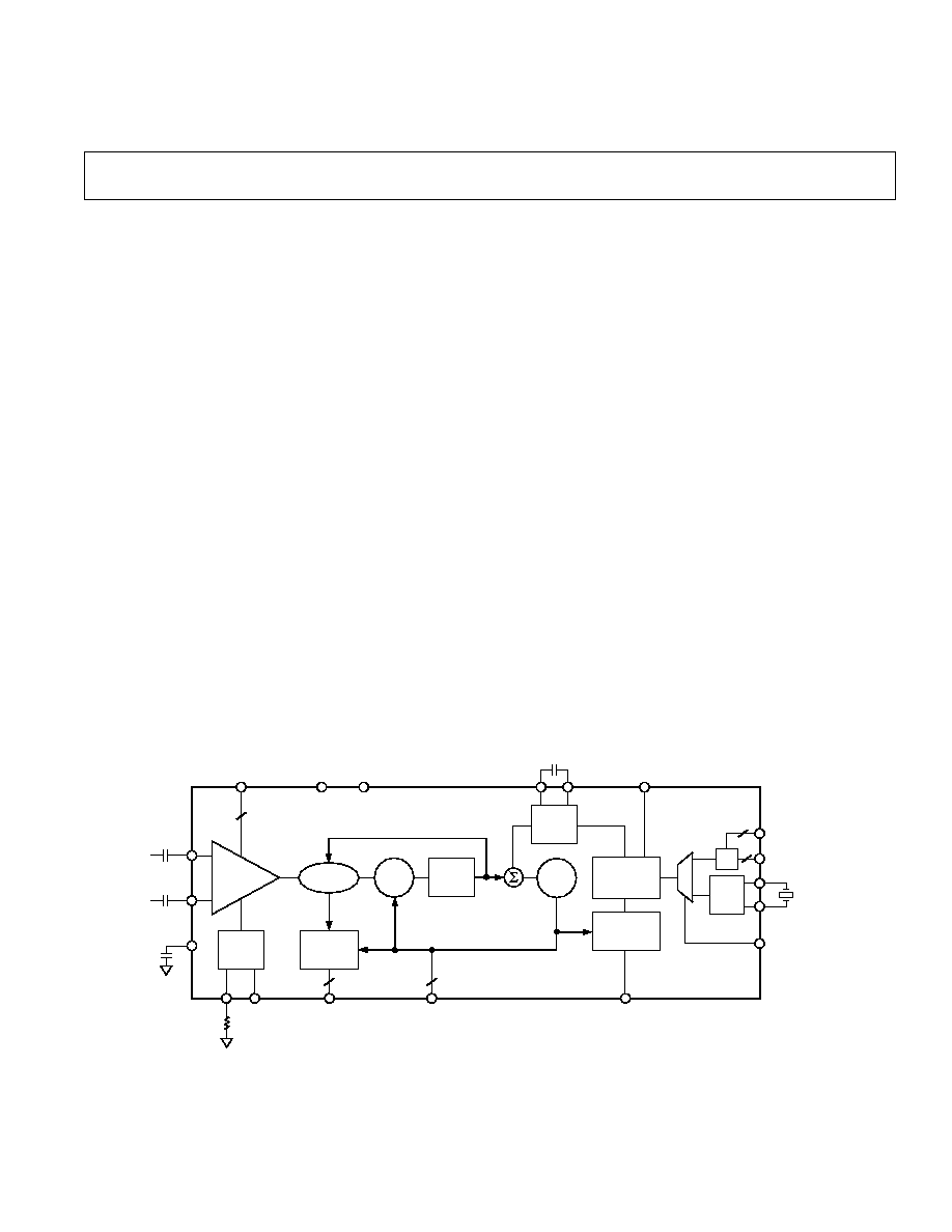
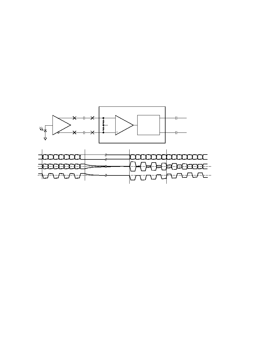
FUNCTIONAL BLOCK DIAGRAM
LEVEL
DETECT
DATA
RETIMING
FRACTIONAL
DIVIDER
FREQUENCY
LOCK
DETECTOR
LOOP
FILTER
PHASE
SHIFTER
PHASE
DET.
VCO
XTAL
OSC
LOOP
FILTER
QUANTIZER
/n
ADN2811
SLICEP/N
VCC
VEE
CF1
CF2
LOL
REFSEL[0..1]
REFCLKP/N
XO1
XO2
REFSEL
RATE
CLKOUTP/N
DATAOUTP/N
SDOUT
THRADJ
VREF
NIN
PIN
2
2
2
2
2
PRODUCT DESCRIPTION
The ADN2811 provides the receiver functions of quantization,
signal level detect, and clock and data recovery at OC-48 and
OC-48 FEC rates. All SONET jitter requirements are met,
including jitter transfer, jitter generation, and jitter tolerance.
All specifications are quoted for �40 C to +85 C ambient
temperature, unless otherwise noted.
The device is intended for WDM system applications and can
be used with either an external reference clock or an on-chip
oscillator with external crystal. Both the 2.48 Gb/s and 2.66 Gb/s
digital wrapper rate is supported by the ADN2811, without any
change of reference clock.
This device, together with a PIN diode and a TIA preamplifier,
can implement a highly integrated, low cost, low power, fiber
optic receiver.
The receiver front end signal detect circuit indicates when the
input signal level has fallen below a user-adjustable threshold.
The signal detect circuit has hysteresis to prevent chatter at
the output.
The ADN2811 is available in a compact 7 mm
� 7 mm 48-lead
chip scale package.
REV. A
�2�
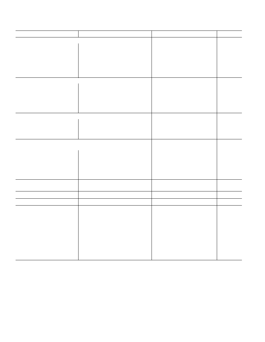
ADN2811�SPECIFICATIONS
(T
A
= T
MIN
to T
MAX
, VCC = V
MIN
to V
MAX
, V
EE
= 0 V, C
F
= 4.7 F, SLICEP = SLICEN = VCC,
unless otherwise noted.)
Parameter
Conditions
Min
Typ
Max
Unit
QUANTIZER�DC CHARACTERISTICS
Input Voltage Range
@ PIN or NIN, DC-Coupled
0
1.2
V
Peak-to-Peak Differential Input
2.4
V
Input Common-Mode Level
DC-Coupled. (See Figure 22)
0.4
V
Differential Input Sensitivity
PIN�NIN, AC-Coupled
1
, BER = 1 10
�10
4
10
mV p-p
Input Overdrive
Figure 4
2
5
mV p-p
Input Offset
500
�V
Input rms Noise
BER = 1
10
�10
244
�V rms
QUANTIZER�AC CHARACTERISTICS
Upper �3 dB Bandwidth
1.9
GHz
Small Signal Gain
Differential
54
dB
S11
@ 2.5 GHz
�15
dB
Input Resistance
Differential
100
Input Capacitance
0.65
pF
Pulsewidth Distortion
2
10
ps
QUANTIZER SLICE ADJUSTMENT
Gain
SliceP�SliceN = 0.5 V
0.115
0.200
0.300
V/V
Control Voltage Range
SliceP�SliceN
�0.8
+0.8
V
Control Voltage Range
@ SliceP or SliceN
1.3
VCC
V
Slice Threshold Offset
�1.0
mV
LEVEL SIGNAL DETECT (SDOUT)
Level Detect Range (See Figure 2)
R
THRESH
= 2 k
9.4
13.3
18.0
mV
R
THRESH
= 20 k
2.5
5.3
7.6
mV
R
THRESH
= 90 k
0.7
3.0
5.2
mV
Response TimeDC-Coupled
0.1
0.3
5
�s
Hysteresis (Electrical), PRBS 2
23
R
THRESH
= 2 k
5.6
6.6
7.8
dB
R
THRESH
= 20 k
3.9
6.1
8.5
dB
R
THRESH
= 90 k
3.2
6.7
9.9
dB
LOSS OF LOCK DETECT (LOL)
LOL Response Time
From f
VCO
error > 1000 ppm
60
�s
POWER SUPPLY VOLTAGE
3.0
3.3
3.6
V
POWER SUPPLY CURRENT
150
164
215
mA
PHASE-LOCKED LOOP
CHARACTERISTICS
PIN�NIN = 10 mV p-p
Jitter Transfer BW
OC-48
590
880
kHz
Jitter Peaking
OC-48
0.025
dB
Jitter Generation
OC-48, 12 kHz�20 MHz
0.003
3
UI rms
0.05
0.09
UI p-p
Jitter Tolerance
OC-48 (See Figure 9)
600 Hz
92
3
UI p-p
6 kHz
20
3
UI p-p
100 kHz
5.5
UI p-p
1 MHz
1.0
3
UI p-p

REV. A
ADN2811
�3�
Parameter
Conditions
Min
Typ
Max
Unit
CML OUTPUTS (CLKOUTP/N, DATAOUTP/N)
Single-Ended Output Swing
V
SE
(See Figure 3)
300
455
600
mV
Differential Output Swing
V
DIFF
(See Figure 3)
600
910
1200
mV
Output High Voltage
V
OH
VCC
V
Output Low Voltage
V
OL
VCC � 0.6
VCC � 0.3
V
Rise Time
20%�80%
84
150
ps
Fall time
80%�20%
84
150
ps
Setup Time
T
S
(See Figure 1)
OC-48
140
ps
Hold Time
T
H
(See Figure 1)
OC-48
150
ps
REFCLK DC INPUT CHARACTERISTICS
Input Voltage Range
@ REFCLKP or REFCLKN
0
VCC
V
Peak-to-Peak Differential Input
100
mV
Common-Mode Level
DC-Coupled, Single-Ended
VCC/2
V
TEST DATA DC INPUT
CHARACTERISTICS
4
(TDINP/N)
CML Inputs
Peak-to-Peak Differential Input Voltage
0.8
V
LVTTL DC INPUT CHARACTERISTICS
Input High Voltage
V
IH
2.0
V
Input Low Voltage
V
IL
0.8
V
Input Current
V
IN
= 0.4 V or V
IN
= 2.4 V
�5
+5
LVTTL DC OUTPUT CHARACTERISTICS
Output High Voltage
V
OH
, I
OH
= �2.0 mA
2.4
V
Output Low Voltage
V
OL
, I
OL
= +2.0 mA
0.4
V
NOTES
1
PIN and NIN should be differentially driven, ac-coupled for optimum sensitivity.
2
PWD measurement made on quantizer outputs in BYPASS mode.
3
Measurement is equipment limited.
4
TDINP/N are CML inputs. If the drivers to the TDINP/N inputs are anything other than CML, they must be ac-coupled.
Specifications subject to change without notice.
REV. A
�4�
ADN2811
ABSOLUTE MAXIMUM RATINGS
*
Supply Voltage (VCC) . . . . . . . . . . . . . . . . . . . . . . . . . . . 5.5 V
Minimum Input Voltage (All Inputs) . . . . . . . . . . VEE � 0.4 V
Maximum Input Voltage (All Inputs) . . . . . . . . VCC + 0.4 V
Maximum Junction Temperature . . . . . . . . . . . . . . . . . 165 C
Storage Temperature . . . . . . . . . . . . . . . . . . �65 C to +150 C
Lead Temperature (Soldering 10 Sec) . . . . . . . . . . . . . . 300 C
*Stresses above those listed under Absolute Maximum Ratings may cause perma-
nent damage to the device. This is a stress rating only; functional operation of the
device at these or any other conditions above those indicated in the operational
section of this specification is not implied. Exposure to absolute maximum rating
conditions for extended periods may affect device reliability.
THERMAL CHARACTERISTICS
Thermal Resistance
48-Lead LFCSP, four-layer board with exposed paddle
soldered to VCC
JA
= 25 C/W
CAUTION
ESD (electrostatic discharge) sensitive device. Electrostatic charges as high as 4000 V readily
accumulate on the human body and test equipment and can discharge without detection. Although the
ADN2811 features proprietary ESD protection circuitry, permanent damage may occur on devices
subjected to high energy electrostatic discharges. Therefore, proper ESD precautions are recommended
to avoid performance degradation or loss of functionality.
ORDERING GUIDE
Model
Temperature Range
Package
Option
ADN2811ACP-CML
�40�C to +85�C
48-Lead LFCSP
CP-48
ADN2811ACP-CML-RL �40�C to +85�C
48-Lead LFCSP
CP-48
Tape-Reel, 2500 pcs
REV. A
ADN2811
�5�
PIN CONFIGURATION
PIN 1
INDICATOR
TOP VIEW
ADN2811
THRADJ 1
VCC 2
VEE 3
VREF 4
PIN 5
NIN 6
SLICEP 7
SLICEN 8
VEE 9
LOL 10
XO1 11
XO2 12
REFCLKN 13
REFCLKP 14
REFSEL 15
VEE 16
TDINP 17
TDINN 18
VEE 19
VCC 20
CF1 21
VEE 22
REFSEL1 23
REFSEL0 24
36 VCC
35 VCC
34 VEE
33 VEE
32 NC
31 NC
30 RATE
29 VEE
28 VCC
27 VEE
26 VCC
25 CF2
48 LOOPEN
47 VCC
46 VEE
45 SDOUT
44 BYP
A
SS
43 VEE
42 VEE
41 CLK
OUTP
40 CLK
OUTN
39 SQ
UELCH
38 D
A
T
A
OUTP
37 D
A
T
A
OUTN
NC = NO CONNECT
PIN FUNCTION DESCRIPTION
Pin No.
Mnemonic
Type
Description
1
THRADJ
AI
LOS Threshold Setting Resistor
2, 26, 28, Pad
VCC
P
Analog Supply
3, 9, 16, 19, 22, 27, 29,
VEE
P
Ground
33, 34, 42, 43, 46
4
VREF
AO
Internal V
REF
Voltage. Decouple to GND with 0.1
�F capacitor.
5
PIN
AI
Differential Data Input. CML.
6
NIN
AI
Differential Data Input. CML.
7
SLICEP
AI
Differential Slice Level Adjust Input
8
SLICEN
AI
Differential Slice Level Adjust Input
10
LOL
DO
Loss of Lock Indicator. LVTTL active high.
11
XO1
AO
Crystal Oscillator
12
XO2
AO
Crystal Oscillator
13
REFCLKN
DI
Differential REFCLK Input. LVTTL, LVCMOS, LVPECL, LVDS
(LVPECL, LVDS only at 155.52 MHz).
14
REFCLKP
DI
Differential REFCLK Input. LVTTL, LVCMOS, LVPECL, LVDS
(LVPECL, LVDS only at 155.52 MHz).
15
REFSEL
DI
Reference Source Select. "0" = on-chip oscillator with external crystal;
"1" = external clock source, LVTTL.
17
TDINP
AI
Differential Test Data Input
18
TDINN
AI
Differential Test Data Input
20, 47
VCC
P
Digital Supply
21
CF1
AO
Frequency Loop Capacitor
23
REFSEL1
DI
Reference Frequency Select (See Table II) LVTTL.
24
REFSEL0
DI
Reference Frequency Select (See Table II) LVTTL.
25
CF2
AO
Frequency Loop Capacitor
30
RATE
DI
Data Rate Select (See Table I) LVTTL.
31, 32
NC
DI
No Connect
35, 36
VCC
P
Output Driver Supply
37
DATAOUTN
DO
Differential Retimed Data Output. CML.
38
DATAOUTP
DO
Differential Retimed Data Output. CML.
39
SQUELCH
DI
Disable Clock and Data Outputs. Active high. LVTTL.
40
CLKOUTN
DO
Differential Recovered Clock Output. CML.
41
CLKOUTP
DO
Differential Recovered Clock Output. CML.
44
BYPASS
DI
Bypass CDR Mode. Active high. LVTTL.
45
SDOUT
DO
Loss of Signal Detect Output. Active high. LVTTL.
48
LOOPEN
DI
Enable Test Data Inputs. Active high. LVTTL.
Type: P = Power, AI = Analog Input, AO = Analog Output, DI = Digital Input, DO = Digital Output
REV. A
�6�
ADN2811
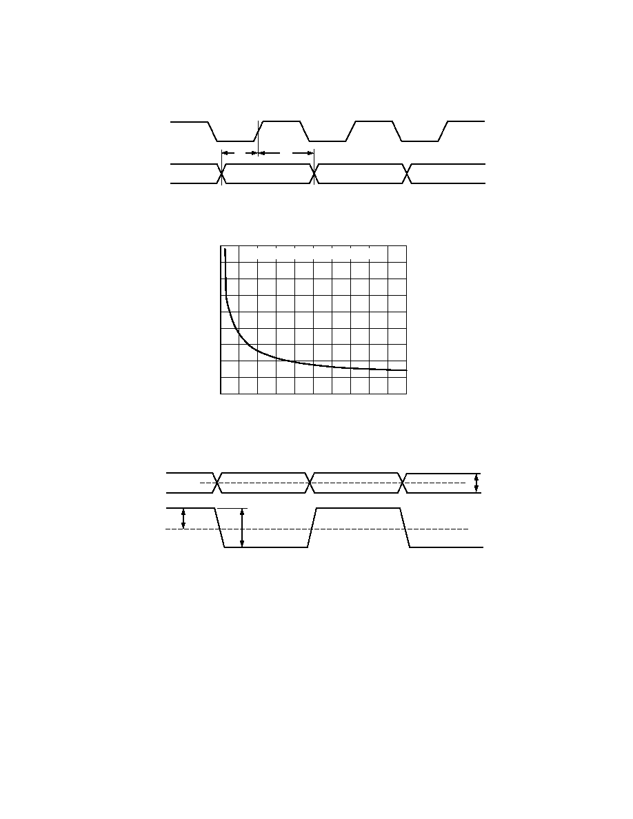
T
S
T
H
CLKOUTP
DATAOUTP/N
Figure 1. Output Timing
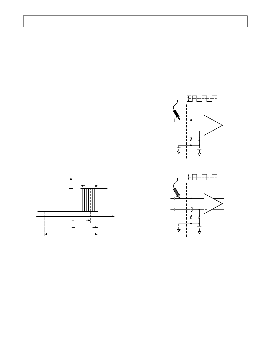
RESISTANCE � k
0
100
10
20
30
40
50
60
70
80
90
18
16
0
mV
8
6
4
2
12
10
14
THRADJ RESISTOR VS. LOS TRIP POINT
Figure 2. LOS Comparator Trip Point Programming
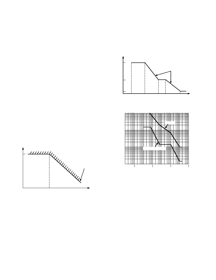
OUTP
OUTN
V
SE
V
CML
0V
OUTP�OUTN
V
SE
V
DIFF
Figure 3. Single-Ended vs. Differential Output Specs
REV. A
ADN2811
�7�
DEFINITION OF TERMS
Maximum, Minimum, and Typical Specifications
Specifications for every parameter are derived from statistical
analyses of data taken on multiple devices from multiple wafer
lots. Typical specifications are the mean of the distribution of
the data for that parameter. If a parameter has a maximum (or a
minimum), that value is calculated by adding to (or subtracting
from) the mean six times the standard deviation of the distribu-
tion. This procedure is intended to tolerate production variations.
If the mean shifts by 1.5 standard deviations, the remaining 4.5
standard deviations still provide a failure rate of only 3.4 parts
per million. For all tested parameters, the test limits are guardbanded
to account for tester variation to thus guarantee that no device is
shipped outside of data sheet specifications.
INPUT SENSITIVITY AND INPUT OVERDRIVE
Sensitivity and overdrive specifications for the quantizer involve
offset voltage, gain, and noise. The relationship between the
logic output of the quantizer and the analog voltage input is
shown in Figure 4. For sufficiently large positive input voltage,
the output is always Logic 1; similarly for negative inputs, the
output is always Logic 0. However, the transitions between
output Logic Levels 1 and 0 are not at precisely defined input
voltage levels but occur over a range of input voltages. Within
this zone of confusion, the output may be either 1 or 0, or it
may even fail to attain a valid logic state. The width of this zone
is determined by the input voltage noise of the quantizer. The
center of the zone of confusion is the quantizer input offset
voltage. Input overdrive is the magnitude of signal required to
guarantee the correct logic level with 1
� 10
�10
confidence level.
0
1
INPUT (V p-p)
OUTPUT
NOISE
SENSITIVITY
(2 OVERDRIVE)
OFFSET
OVERDRIVE
Figure 4. Input Sensitivity and Input Overdrive
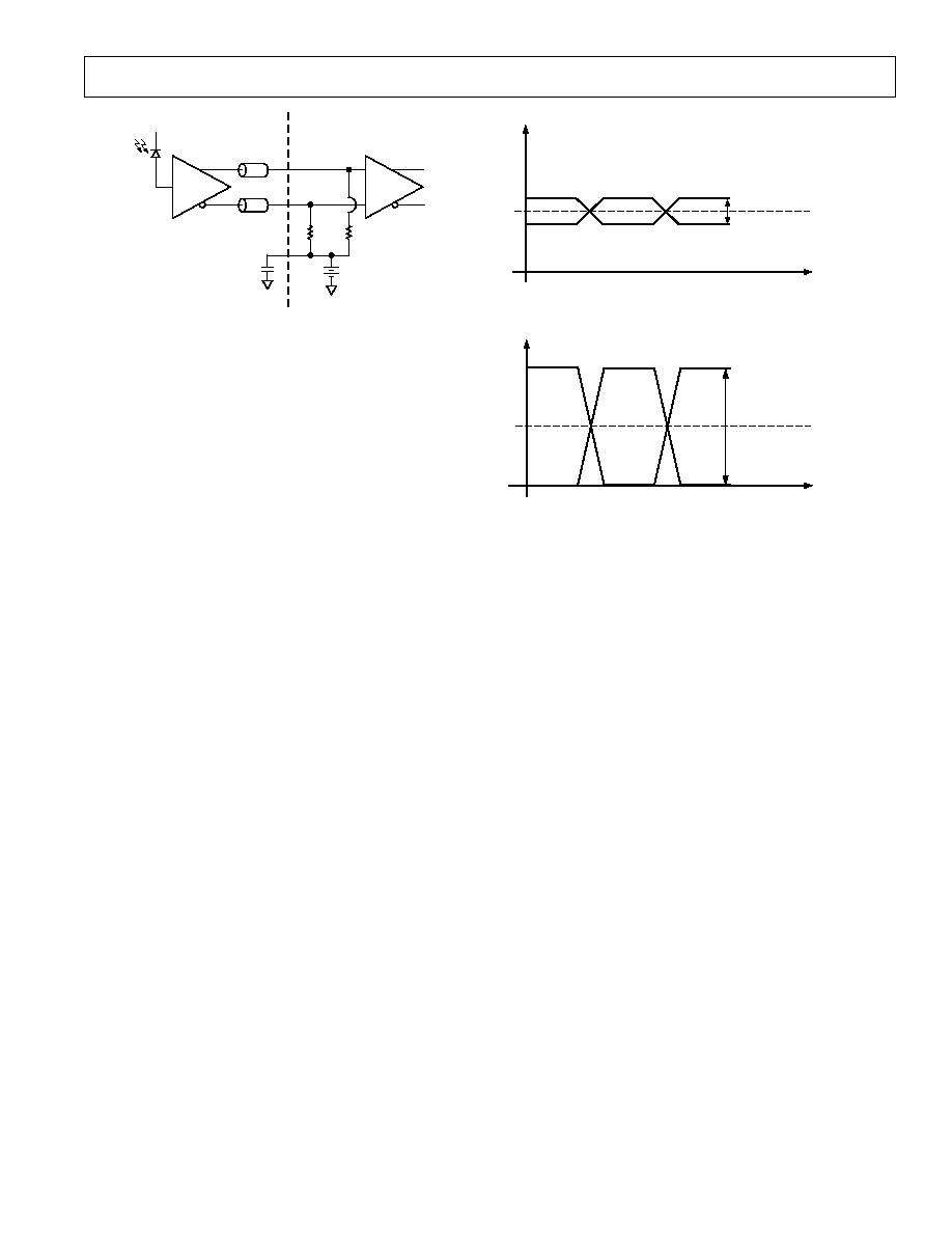
SINGLE-ENDED VS. DIFFERENTIAL
AC-coupling is typically used to drive the inputs to the quan-
tizer. The inputs are internally dc biased to a common-mode
potential of ~0.6 V. Driving the ADN2811 single-ended and
observing the quantizer input with an oscilloscope probe at the
point indicated in Figure 5 shows a binary signal with an average
value equal to the common-mode potential and instantaneous
values both above and below the average value. It is convenient
to measure the peak-to-peak amplitude of this signal and call
the minimum required value the quantizer sensitivity. Referring
to Figure 4, since both positive and negative offsets need to be
accommodated, the sensitivity is twice the overdrive.
50
50
QUANTIZER
+
ADN2811
VREF
PIN
SCOPE
PROBE
VREF
10mV p-p
Figure 5. Single-Ended Sensitivity Measurement
50
50
QUANTIZER
+
ADN2811
VREF
NIN
PIN
SCOPE
PROBE
VREF
5mV p-p
Figure 6. Differential Sensitivity Measurement
Driving the ADN2811 differentially (see Figure 6), sensitivity
seems to improve by observing the quantizer input with an
oscilloscope probe. This is an illusion caused by the use of a
single-ended probe. A 5 mV p�p signal appears to drive the
ADN2811 quantizer. However, the single-ended probe mea-
sures only half the signal. The true quantizer input signal is
twice this value since the other quantizer input is a complemen-
tary signal to the signal being observed.
LOS Response Time
The LOS response time is the delay between the removal of
the input signal and the indication of loss of signal (LOS) at
SDOUT. The LOS response time of the ADN2811 is 300 ns
typ when the inputs are dc-coupled. In practice, the time con-
stant of the ac-coupling at the quantizer input determines the
LOS response time.
REV. A
�8�
ADN2811
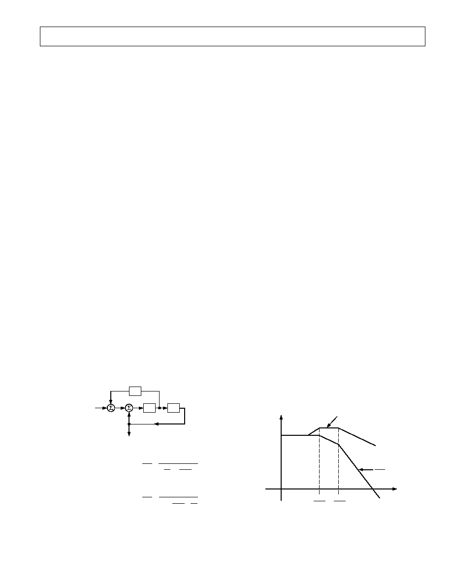
JITTER SPECIFICATIONS
The ADN2811 CDR is designed to achieve the best bit-error-rate
(BER) performance and has exceeded the jitter generation, trans-
fer, and tolerance specifications proposed for SONET/SDH
equipment defined in the Telcordia Technologies specification.
Jitter is the dynamic displacement of digital signal edges from
their long-term average positions measured in UI (unit intervals),
where 1 UI = 1 bit period. Jitter on the input data can cause
dynamic phase errors on the recovered clock sampling edge.
Jitter on the recovered clock causes jitter on the retimed data.
The following section briefly summarizes the specifications of
the jitter generation, transfer, and tolerance in accordance with
the Telcordia document (GR-253-CORE, Issue 3, September
2000) for the optical interface at the equipment level and the
ADN2811 performance with respect to those specifications.
Jitter Generation
The jitter generation specification limits the amount of jitter
that can be generated by the device with no jitter and wander
applied at the input. For OC-48 devices, the band-pass filter has
a 12 kHz high-pass cutoff frequency with a roll-off of 20 dB/
decade and a low-pass cutoff frequency of at least 20 MHz. The
jitter generated should be less than 0.01 UI rms and less
than 0.1 UI p-p.
Jitter Transfer
The jitter transfer function is the ratio of the jitter on the output
signal to the jitter applied on the input signal versus the fre-
quency. This parameter measures the limited amount of jitter
on an input signal that can be transferred to the output signal
(see Figure 7).
SLOPE = �20dB/DECADE
JITTER FREQUENCY � kHz
0.1
JITTER GAIN � dB
f
C
ACCEPTABLE
RANGE
Figure 7. Jitter Transfer Curve
Jitter Tolerance
The jitter tolerance is defined as the peak-to-peak amplitude of
the sinusoidal jitter applied on the input signal that causes a
1 dB power penalty. This is a stress test that is intended to
ensure no additional penalty is incurred under the operating
conditions (see Figure 8). Figure 9 shows the typical OC-48
jitter tolerance performance of the ADN2811.
SLOPE = �20dB/DECADE
f
0
f
1
f
2
f
3
f
4
JITTER FREQUENCY � Hz
15
1.5
0.15
INPUT JITTER AMPLITUDE � UI p-p
Figure 8. SONET Jitter Tolerance Mask
MODULATION FREQUENCY � Hz
1.00E+01
1.00E+03
1.00E+05
1.00E+07
1.00E+02
1.00E+01
1.00E�01
AMPLITUDE � UI p-p 1.00E+00
1.00E+02
1.00E+04
1.00E+06
1.00E+00
ADN2811
OC-48 SONET MASK
Figure 9. OC-48 Jitter Tolerance Curve
REV. A
ADN2811
�9�
THEORY OF OPERATION
The ADN2811 is a delay-locked and phase-locked loop circuit
for clock recovery and data retiming from an NRZ encoded data
stream. The phase of the input data signal is tracked by two
separate feedback loops that share a common control voltage.
A high speed delay-locked loop path uses a voltage controlled
phase shifter to track the high frequency components of the
input jitter. A separate phase control loop, comprised of the
VCO, tracks the low frequency components of the input jitter.
The initial frequency of the VCO is set by yet a third loop, which
compares the VCO frequency with the reference frequency and
sets the coarse tuning voltage. The jitter tracking phase-locked
loop controls the VCO by the fine tuning control.
The delay-locked and phase-locked loops together track the
phase of the input data signal. For example, when the clock lags
input data, the phase detector drives the VCO to a higher
frequency and also increases the delay through the phase shifter.
Both of these actions both serve to reduce the phase error between
the clock and data. The faster clock picks up phase while the
delayed data loses phase. Since the loop filter is an integrator,
the static phase error will be driven to zero.
Another view of the circuit is that the phase shifter implements
the zero required for the frequency compensation of a second-
order phase-locked loop, and this zero is placed in the feedback
path and thus does not appear in the closed-loop transfer func-
tion. Jitter peaking in a conventional second-order phase-locked
loop is caused by the presence of this zero in the closed-loop
transfer function. Since this circuit has no zero in the closed-
loop transfer, jitter peaking is minimized.
The delay-locked and phase-locked loops together simultaneously
provide wideband jitter accommodation and narrow-band jitter
filtering. The linearized block diagram in Figure 10 shows the
jitter transfer function, Z(s)/X(s), is a second-order low-pass
providing excellent filtering. Note the jitter transfer has no zero,
unlike an ordinary second-order phase-locked loop. This means
that the main PLL loop has low jitter peaking (see Figure 11),
which makes this circuit ideal for signal regenerator applications
where jitter peaking in a cascade of regenerators can contribute
to hazardous jitter accumulation.
d/sc
psh
e(s)
X(s)
INPUT
DATA
Z(s)
RECOVERED
CLOCK
d = PHASE DETECTOR GAIN
o = VCO GAIN
c = LOOP INTEGRATOR
psh = PHASE SHIFTER GAIN
n = DIVIDE RATIO
JITTER TRANSFER FUNCTION
Z(s)
X(s)
1
s
2
+ s +1
cn
do
n psh
o
=
TRACKING ERROR TRANSFER FUNCTION
e(s)
X(s)
s
2
s
2
+ s +
do
cn
d psh
c
=
o/s
Figure 10. PLL/DLL Architecture
The error transfer, e(s)/X(s), has the same high-pass form as an
ordinary phase-locked loop. This transfer function is free to be
optimized to give excellent wideband jitter accommodation
since the jitter transfer function, Z(s)/X(s), provides the narrow-
band jitter filtering.
The delay-locked and phase-locked loops contribute to overall
jitter accommodation. At low frequencies of input jitter on the
data signal, the integrator in the loop filter provides high gain to
track large jitter amplitudes with small phase error. In this case,
the VCO is frequency modulated and jitter is tracked as in an
ordinary phase-locked loop. The amount of low frequency jitter
that can be tracked is a function of the VCO tuning range. A
wider tuning range gives larger accommodation of low fre-
quency jitter. The internal loop control voltage remains small
for small phase errors, so the phase shifter remains close to the
center of its range and thus contributes little to the low fre-
quency jitter accommodation.
At medium jitter frequencies, the gain and tuning range of the
VCO are not large enough to track the input jitter. In this case,
the VCO control voltage becomes large and saturates, and the
VCO frequency dwells at one or the other extreme of its tuning
range. The size of the VCO tuning range therefore has only a
small effect on the jitter accommodation. The delay-locked loop
control voltage is now larger, and so the phase shifter takes on
the burden of tracking the input jitter. The phase shifter range, in
UI, can be seen as a broad plateau on the jitter tolerance curve.
The phase shifter has a minimum range of 2 UI at all data rates.
The gain of the loop integrator is small for high jitter frequen-
cies, so larger phase differences are needed to make the loop
control voltage big enough to tune the range of the phase
shifter. Large phase errors at high jitter frequencies cannot be
tolerated. In this region, the gain of the integrator determines
the jitter accommodation. Since the gain of the loop integrator
declines linearly with frequency, jitter accommodation is lower
with higher jitter frequency. At the highest frequencies, the loop
gain is very small and little tuning of the phase shifter can be
expected. In this case, jitter accommodation is determined by
the eye opening of the input data, the static phase error, and the
residual loop jitter generation. The jitter accommodation is
roughly 0.5 UI in this region. The corner frequency between the
declining slope and the flat region is the closed loop bandwidth
of the delay-locked loop, which is roughly 5 MHz.
JITTER PEAKING
IN ORDINARY PLL
ADN2811
Z(s)
X(s)
f
(kHz)
JITTER
GAIN
(dB)
o
n psh
d psh
c
Figure 11. Jitter Response vs. Conventional PLL
REV. A
�10�
ADN2811
FUNCTIONAL DESCRIPTION
Clock and Data Recovery
The ADN2811 will recover clock and data from serial bit streams
at OC-48 as well as the 15/14 FEC rates. The data rate is selected
by the RATE input (see Table I).
Table I. Data Rate Selection
RATE
Data Rate
Frequency (MHz)
0
OC-48
2488.32
1
OC-48 FEC
2666.06
Limiting Amplifier
The limiting amplifier has differential inputs (PIN/NIN) that are
internally terminated with 50
to an on-chip voltage reference
(VREF = 0.6 V typically). These inputs are normally ac-coupled,
although dc-coupling is possible as long as the input common-mode
voltage remains above 0.4 V (see Figures 20�22). Input offset is
factory trimmed to achieve better than 4 mV typical sensitivity
with minimal drift. The limiting amplifier can be driven
differentially or single-ended.
Slice Adjust
The quantizer slicing level can be offset by
� 100 mV to mitigate
the effect of ASE (amplified spontaneous emission) noise by
applying a differential voltage input of
� 0.8 V to SLICEP/N
inputs. If no adjustment of the slice level is needed, SLICEP/N
should be tied to VCC.
Loss of Signal (LOS) Detector
The receiver front end level signal detect circuit indicates when
the input signal level has fallen below a user adjustable threshold.
The threshold is set with a single external resistor from Pin 1,
THRADJ, to GND. The LOS comparator trip point versus the
resistor value is illustrated in Figure 2 (this is only valid for
SLICEP = SLICEN = VCC). If the input level to the ADN2811
drops below the programmed LOS threshold, SDOUT (Pin 45)
will indicate the loss of signal condition with a Logic 1. The LOS
response time is ~300 ns by design but will be dominated by the
RC time constant in ac-coupled applications.
If the LOS detector is used, the quantizer slice adjust pins must
both be tied to VCC. This is to avoid interaction with the LOS
threshold level.
Note that it is not expected to use both LOS and slice adjust at
the same time; systems with optical amplifiers need the slice
adjust to evade ASE. However, a loss of signal in an optical link
that uses optical amplifiers causes the optical amplifier output to
be full-scale noise. Under this condition, the LOS would not
detect the failure. In this case, the loss of lock signal will indi-
cate the failure because the CDR circuitry will not be able to
lock onto a signal that is full-scale noise.
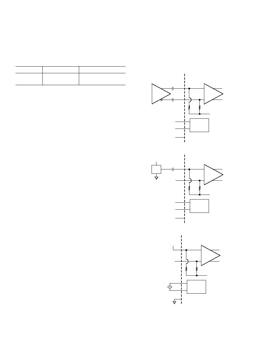
Reference Clock
There are three options for providing the reference frequency to
the ADN2811: differential clock, single-ended clock, or crystal
oscillator. See Figures 12�14 for example configurations.
The ADN2811 can accept any of the following reference clock
frequencies: 19.44 MHz, 38.88 MHz, 77.76 MHz at LVTTL/
LVCMOS/LVPECL/LVDS levels or 155.52 MHz at LVPECL/
LVDS levels via the REFCLKN/P inputs, independent of data
rate. The input buffer accepts any differential signal with a
peak-to-peak differential amplitude of greater than 100 mV
(e.g., LVPECL or LVDS) or a standard single-ended low volt-
age TTL input, providing maximum system flexibility. The
appropriate division ratio can be selected using the REFSEL0/1
pins, according to Table II. Phase noise and duty cycle of the
reference clock are not critical and 100 ppm accuracy is sufficient.
100k
100k
BUFFER
ADN2811
VCC/2
REFCLKN
REFCLKP
CRYSTAL
OSCILLATOR
XO1
XO2
VCC
VCC
VCC
REFSEL
Figure 12. Differential REFCLK Configuration
OUT
100k
100k
BUFFER
ADN2811
VCC/2
REFCLKP
CRYSTAL
OSCILLATOR
XO1
XO2
VCC
VCC
VCC
REFSEL
CLK
OSC
VCC
REFCLKN
NC
Figure 13. Single-Ended REFCLK Configuration
100k
100k
BUFFER
ADN2811
VCC/2
REFCLKN
REFCLKP
CRYSTAL
OSCILLATOR
XO1
XO2
REFSEL
NC
19.44MHz
VCC
Figure 14. Crystal Oscillator Configuration
REV. A
ADN2811
�11�
An on-chip oscillator to be used with an external crystal is also
provided as an alternative to using the REFCLKN/P inputs.
Details of the recommended crystal are given in Table III.
Table II. Reference Frequency Selection
Applied Reference
REFSEL
REFSEL[1..0]
Frequency (MHz)
1
00
19.44
1
01
38.88
1
10
77.76
1
11
155.52
0
XX
REFCLKP/N Inactive. Use
19.44 MHz XTAL oscillator
on Pins XO1, XO2 (Pull
REFCLKP to VCC).
Table III. Required Crystal Specifications
Parameter
Value
Mode
Series Resonant
Frequency/Overall Stability
19.44 MHz
� 100 ppm
Frequency Accuracy
� 100 ppm
Temperature Stability
� 100 ppm
Aging
� 100 ppm
ESR
20
max
Recommended Manufacturer:
Raltron (305) 593-6033
Part Number: H10S-19.440-S-EXT
REFSEL must be tied to VCC when the REFCLKN/P inputs
are active or tied to VEE when the oscillator is used. No
connection between the XO pin and REFCLK input is necessary
(see Figures 12�14). Note that the crystal should operate in series
resonant mode, which renders it insensitive to external parasitics.
No trimming capacitors are required.
Lock Detector Operation
The lock detector monitors the frequency difference between
the VCO and the reference clock and deasserts the loss of lock
signal when the VCO is within 500 ppm of center frequency
(see Figure 15). This enables the phase loop, which pulls the
VCO frequency in the remaining amount and also acquires
phase lock. Once locked, if the input frequency error exceeds
1000 ppm (0.1%), the loss of lock signal is reasserted and con-
trol returns to the frequency loop, which will reacquire and
maintain a stable clock signal at the output.
1000
500
0
500
1000
f
VCO
ERROR
(ppm)
LOL
1
Figure 15. Transfer Function of LOL
The frequency loop requires a single external capacitor between
CF1 and CF2. The capacitor specification is given in Table IV.
Table IV. Recommended C
F
Capacitor Specification
Parameter
Value
Temperature Range
�40 C to +85 C
Capacitance
>3.0
�F
Leakage
<80 nA
Rating
>6.3 V
Recommended Manufacturer:
Murata Electronics (770) 436-1300
Part Number: GRM32RR71C475LC01
Squelch Mode
When the squelch input is driven to a TTL high state, both the
clock and data outputs are set to the zero state to suppress
downstream processing. If desired, this pin can be directly
driven by the LOS detector output, SDOUT. If the squelch func-
tion is not required, the pin should be tied to VEE.
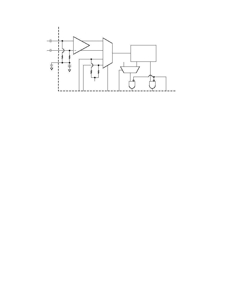
Test Modes: Bypass and Loopback
When the bypass input is driven to a TTL high state, the
quantizer output is connected directly to the buffers driving the data
out pins, thus bypassing the clock recovery circuit (see Figure 16).
This feature can help the system to deal with nonstandard bit rates.
The Loopback Mode can be invoked by driving the LOOPEN
Pin to a TTL high state, which facilitates system diagnostic test-
ing. This will connect the test inputs (TDINP/N) to the clock
and data recovery circuit (per Figure 16). The test inputs have
internal 50
terminations and can be left floating when not in
use. TDINP/N are CML inputs and can only be dc-coupled
when being driven by CML outputs. The TDINP/N inputs must
be ac-coupled if being driven by anything other than CML out-
puts. Bypass and loopback modes are mutually exclusive. Only
one of these modes can be used at any given time. The
ADN2811 will be put into an indeterminate state if both
BYPASS and LOOPEN pins are set to Logic 1 at the same time.
�12�
REV. A
ADN2811
APPLICATIONS INFORMATION
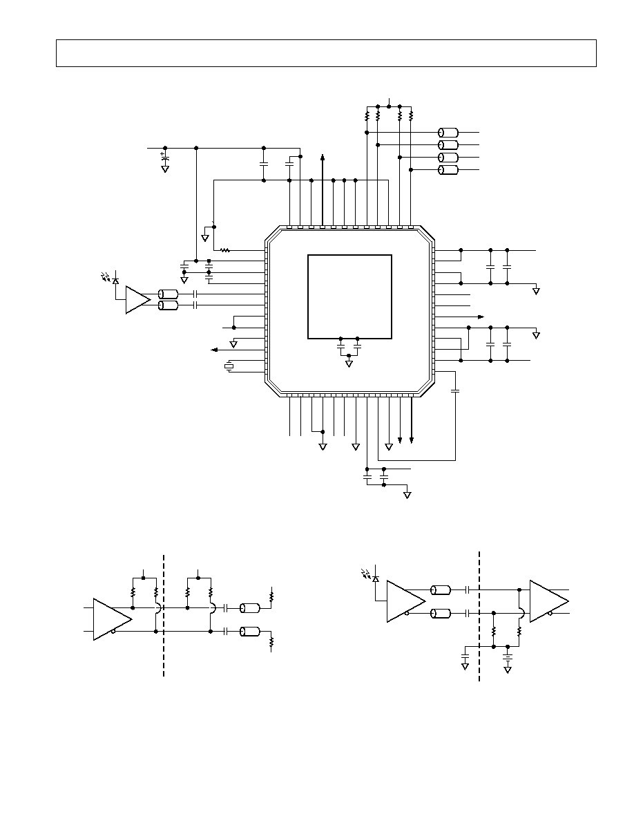
PCB Design Guidelines
Proper RF PCB design techniques must be used for optimal performance.
Power Supply Connections and Ground Planes
Use of one low impedance ground plane to both analog and
digital grounds is recommended. The VEE pins should be sol-
dered directly to the ground plane to reduce series inductance.
If the ground plane is an internal plane and connections to the
ground plane are made through vias, multiple vias may be used
in parallel to reduce the series inductance, especially on Pins 33
and 34, which are the ground returns for the output buffers.
Use of a 10
�F electrolytic capacitor between VCC and GND is
recommended at the location where the 3.3 V supply enters the
PCB. Use of 0.1
�F and 1 nF ceramic chip capacitors should be
placed between IC power supply VCC and GND as close as
possible to the ADN2811 VCC pins. Again, if connections to the
supply and ground are made through vias, the use of multiple vias
in parallel will help to reduce series inductance, especially on Pins 35
and 36, which supply power to the high speed CLKOUTP/N and
DATAOUTP/N output buffers. Refer to the schematic in
Figure 17 for recommended connections.
Transmission Lines
Use of 50
transmission lines are required for all high fre-
quency input and output signals to minimize reflections,
including PIN, NIN, CLKOUTP, CLKOUTN, DATAOUTP,
and DATAOUTN (also REFCLKP, REFCLKN for a
155.2 MHz REFCLK). It is also recommended that the
PIN/NIN input traces are matched in length and that the
50
50
QUANTIZER
+
ADN2811
VREF
NIN
PIN
50
50
VCC
TDINP/N
LOOPEN
BYPASS
CDR
RETIMED
DATA
CLK
0
1
1
0
DATAOUTP/N
CLKOUTP/N SQUELCH
FROM
QUANTIZER
OUTPUT
Figure 16. Test Modes
CLKOUTP/N and DATAOUTP/N output traces are matched
in length. All high speed CML outputs, CLKOUTP/N and
DATAOUTP/N, also require 100
back termination chip
resistors connected between the output pin and VCC. These
resistors should be placed as close as possible to the output
pins. These 100
resistors are in parallel with on-chip 100
termination resistors to create a 50
back termination (see
Figure 18).
The high speed inputs, PIN and NIN, are internally terminated
with 50
to an internal reference voltage (see Figure 19). A 0.1 �F
capacitor is recommended between VREF, Pin 4, and GND to
provide an ac ground for the inputs.
As with any high speed mixed-signal design, take care to keep
all high speed digital traces away from sensitive analog nodes.
Soldering Guidelines for Chip-Scale Package
The lands on the 48-lead LFCSP are rectangular. The printed
circuit board pad for these should be 0.1 mm longer than the
package land length and 0.05 mm wider than the package land
width. The land should be centered on the pad. This will ensure
that the solder joint size is maximized. The bottom of the chip-
scale package has a central exposed pad. The pad on the printed
circuit board should be at least as large as this exposed pad.
The user must connect the exposed pad to analog VCC.
If vias are used, they should be incorporated into the pad at
1.2 mm pitch grid. The via diameter should be between 0.3 mm
and 0.33 mm and the via barrel should be plated with 1 oz.
copper to plug the via.
REV. A
ADN2811
�13�
ADN2811
1
2
3
4
5
6
7
8
9
10
11
12
13 14 15 16 17 18 19 20 21 22 23 24
36
35
34
33
32
31
30
29
28
27
26
25
48 47 46 45 44 43 42 41 40 39 38 37
1nF
0.1 F
1nF
0.1 F
THRADJ
VCC
VEE
VREF
PIN
NIN
SLICEP
SLICEN
VEE
LOL
XO1
XO2
VCC
C
IN
50
R
TH
1nF
0.1 F
0.1 F
50
TIA
VCC
19.44MHz
C
REFCLKN
REFCLKP
REFSEL
VEE
TDINP
TDINN
VEE
VCC
CF1
VEE
REFSEL1
REFSEL0
NC
VCC
NC
NC
C
C
4.7 F
(SEE TABLE IV FOR SPECS)
1nF
0.1 F
VCC
VCC
VCC
VEE
VEE
NC
NC
RATE
VEE
VCC
VEE
VCC
CF2
VCC
LOOPEN
VCC
VEE
SDOUT
BYP
A
SS
VEE
VEE
CLK
OUTP
CLK
OUTN
SQ
UELCH
DA
T
A
OUTP
DA
T
A
OUTN
C
1nF
0.1 F
10 F
VCC
50
TRANSMISSION
LINES
CLKOUTP
CLKOUTN
DATAOUTP
DATAOUTN
VCC
4 100
EXPOSED PAD
TIED OFF TO
VCC PLANE
WITH VIAS
1nF
0.1 F
C
VCC
Figure 17. Typical Application Circuit
100
50
ADN2811
50
50
100
VCC
100
100
VCC
0.1 F
0.1 F
50
V
TERM
V
TERM
Figure 18. AC-Coupled Output Configuration
50
50
ADN2811
0.1 F
NIN
PIN
C
IN
C
IN
50
TIA
VREF
VCC
50
Figure 19. AC-Coupled Input Configuration
�14�
REV. A
ADN2811
Choosing AC-Coupling Capacitors
The choice of ac-coupling capacitors at the input (PIN, NIN)
and output (DATAOUTP, DATAOUTN) of the ADN2811
must be chosen carefully. When choosing the capacitors, the
time constant formed with the two 50
resistors in the signal
path must be considered. When a large number of consecutive
identical digits (CIDs) are applied, the capacitor voltage can
drop due to baseline wander (see Figure 20), causing pattern
dependent jitter (PDJ).
For the ADN2811 to work robustly at OC-48, a minimum
capacitor of 0.1
�F to PIN/NIN and 0.1 �F on DATAOUTP/
DATAOUTN should be used. This is based on the assumption
that 1000 CIDs must be tolerated and that the PDJ should be
limited to 0.01 UI p-p.
50
ADN2811
NIN
PIN
50
V
REF
C
IN
C
IN
V2
V1
V2b
V1b
TIA
LIMAMP
CDR
C
OUT
C
OUT
DATAOUTP
DATAOUTN
+
4
3
2
1
V1
V1b
V2
V2b
V
DIFF
V
DIFF
= V2�V2b
VTH = ADN2811 QUANTIZER THRESHOLD
V
REF
VTH
NOTES
1. DURING DATA PATERNS WITH HIGH TRANSITION DENSITY, DIFFERENTIAL DC VOLTAGE AT V1 AND V2 IS ZERO.
2. WHEN THE OUTPUT OF THE TIA GOES TO CID, V1 AND V1b ARE DRIVEN TO DIFFERENT DC LEVELS. V2 AND V2b DISCHARGE TO THE V
REF
LEVEL, WHICH
EFFECTIVELY INTRODUCES A DIFFERENTIAL DC OFFSET ACROSS THE AC-COUPLING CAPACITORS.
3. WHEN THE BURST OF DATA STARTS AGAIN, THE DIFFERENTIAL DC OFFSET ACROSS THE AC-COUPLING CAPACITORS IS APPLIED TO THE INPUT LEVELS,
CAUSING A DC SHIFT IN THE DIFFERENTIAL INPUT. THIS SHIFT IS LARGE ENOUGH SUCH THAT ONE OF THE STATES, EITHER HIGH OR LOW DEPENDING ON
THE LEVELS OF V1 AND V1b WHEN THE TIA WENT TO CID, IS CANCELLED OUT. THE QUANTIZER WILL NOT RECOGNIZE THIS AS A VALID STATE.
4. THE DC OFFSET SLOWLY DISCHARGES UNTIL THE DIFFERENTIAL INPUT VOLTAGE EXCEEDS THE SENSITIVITY OF THE ADN2811. THE QUANTIZER WILL BE
ABLE TO RECOGNIZE BOTH HIGH AND LOW STATES AT THIS POINT.
Figure 20. Example of Baseline Wander
DC-Coupled Application
The inputs to the ADN2811 can also be dc-coupled. This may
be necessary in burst mode applications where there are long
periods of CIDs and baseline wander cannot be tolerated. If the
inputs to the ADN2811 are dc-coupled, care must be taken not
to violate the input range and common-mode level requirements
of the ADN2811 (see Figures 21�23). If dc-coupling is required,
and the output levels of the TIA do not adhere to the levels
shown in Figures 22 and 23, then there will need to be level
shifting and/or an attenuator between the TIA outputs and the
ADN2811 inputs.
REV. A
ADN2811
�15�
50
50
ADN2811
0.1 F
NIN
PIN
50
TIA
VREF
VCC
50
Figure 21. ADN2811 with DC-Coupled Inputs
LOL Toggling during Loss of Input Data
If the input data stream is lost due to a break in the optical link
(or for any reason), the clock output from the ADN2811 will
stay within 1000 ppm of the VCO center frequency as long as
there is a valid reference clock. The LOL pin will toggle at a
rate of several kHz. This is because the LOL pin will toggle
between a Logic 1 and a Logic 0 while the frequency loop and
phase loop swap control of the VCO. The chain of events are as
follows:
� The ADN2811 is locked to the input data stream; LOL = 0.
� The input data stream is lost due to a break in the link. The
VCO frequency drifts until the frequency error is greater
than 1000 ppm. LOL is asserted to a Logic 1 as control of
the VCO is passed back to the frequency loop.
� The frequency loop pulls the VCO to within 500 ppm of its
center frequency. Control of the VCO is passed back to the
phase loop and LOL is deasserted to a Logic 0.
� The phase loop tries to acquire, but there is no input
data present so the VCO frequency drifts.
� The VCO frequency drifts until the frequency error is
greater than 1000 ppm. LOL is asserted to a Logic 1 as
control of the VCO is passed back to the frequency
loop. This process is repeated until a valid input data
stream is re-established.
V
CM
= 0.4V MIN
(DC-COUPLED)
V
SE
= 5mV MIN
PIN
NIN
V p-p = PIN � NIN = 2 V
SE
= 10mV AT SENSITIVITY
INPUT (V)
Figure 22. Minimum Allowed DC-Coupled Input Levels
INPUT (V)
PIN
NIN
V
CM
= 0.6V
(DC-COUPLED)
V
SE
= 1.2V MAX
V p-p = PIN � NIN = 2 V
SE
= 2.4V MAX
Figure 23. Maximum Allowed DC-Coupled Input Levels
C03019�0�1
2
/02(A)
PRINTED IN U.S.A.
�16�
ADN2811
REV. A
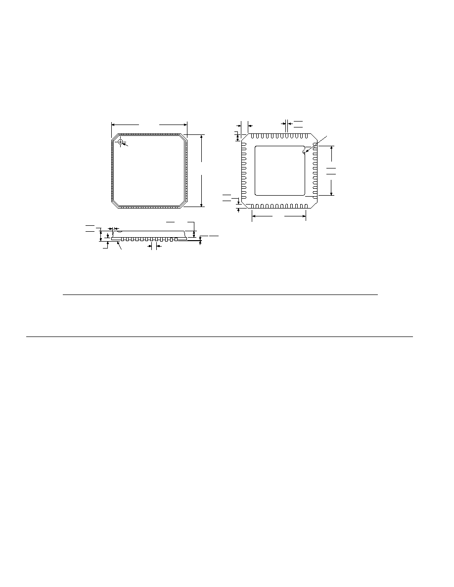
OUTLINE DIMENSIONS
48-Lead Frame Chip Scale Package [LFCSP]
7 mm 7 mm Body
(CP-48)
Dimensions shown in millimeters
PIN 1
INDICATOR
TOP
VIEW
6.75
BSC SQ
7.00
BSC SQ
1
48
12
13
37
36
24
25
BOTTOM
VIEW
5.25
5.10
4.95
0.50
0.40
0.30
0.30
0.23
0.18
0.50 BSC
12
MAX
0.20
REF
1.00 MAX
0.65 NOM
1.00
0.90
0.80
5.50
REF
0.05 MAX
0.02 NOM
0.60 MAX
0.60 MAX
PIN 1
INDICATOR
COPLANARITY
0.08
SQ
SEATING
PLANE
COMPLIANT TO JEDEC STANDARDS MO-220-VKKD-2
Revision History
Location
Page
1
2/02--Data Sheet changed from REV. 0 to REV. A.
Change to FUNCTIONAL DESCRIPTION Reference Clock . . . . . . . . . . . . . . . . . . . . . . . . . . . . . . . . . . . . . . . . . . . . . . . . . . . . 10
Updated OUTLINE DIMENSIONS . . . . . . . . . . . . . . . . . . . . . . . . . . . . . . . . . . . . . . . . . . . . . . . . . . . . . . . . . . . . . . . . . . . . . . . 16