 | ÐлекÑÑоннÑй компоненÑ: ADR1500 | СкаÑаÑÑ:  PDF PDF  ZIP ZIP |
ADR1500 1.2875 V Micropower, Shunt Voltage Reference Data Sheet (Rev. 0)
1.2875 V Micropower, Shunt
Voltage Reference
ADR1500
Rev. 0
Information furnished by Analog Devices is believed to be accurate and reliable. However, no
responsibility is assumed by Analog Devices for its use, nor for any infringements of patents or other
rights of third parties that may result from its use. Specifications subject to change without notice. No
license is granted by implication or otherwise under any patent or patent rights of Analog Devices.
Trademarks and registered trademarks are the property of their respective owners.
One Technology Way, P.O. Box 9106, Norwood, MA 02062-9106, U.S.A.
Tel: 781.329.4700
www.analog.com
Fax: 781.461.3113
©2006 Analog Devices, Inc. All rights reserved.
FEATURES
Wide operating range: 50 A to 10 mA
Initial accuracy: ±0.2% max
Output impedance: 1 max
Wideband noise (10 Hz to 10 kHz): 20 V rms
Operating temperature: -40°C to +85°C
Compact, surface-mount SC70 package
APPLICATIONS
Computer servers
Battery-powered instrumentation
Portable medical equipment
Automotive
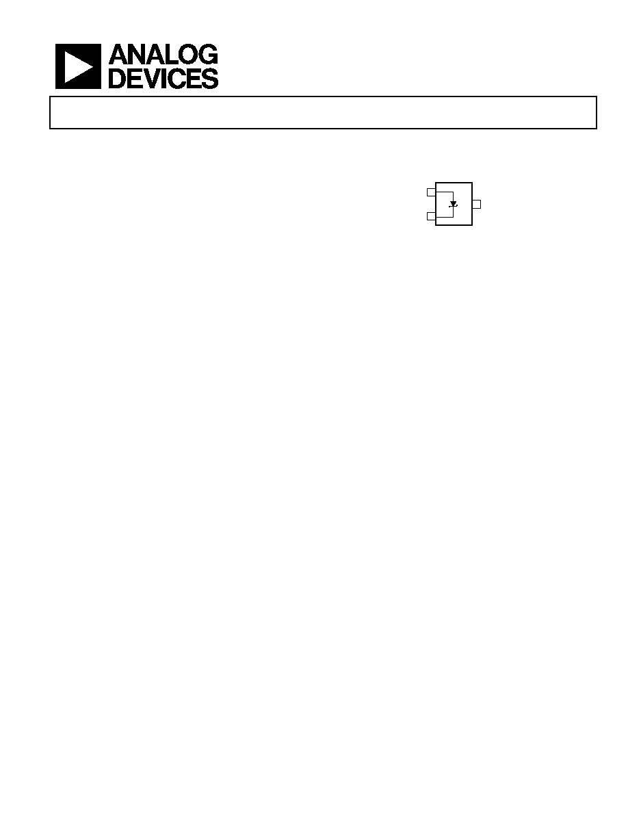
PIN CONFIGURATION
05
74
9-
0
0
1
V
1
V+
2
NC (OR V)
3
TOP VIEW
(Not to Scale)
NC = NO CONNECT
ADR1500
Figure 1. 3-Lead SC70 (KS Suffix)
GENERAL DESCRIPTION
The ADR1500 is a low cost, 2-terminal (shunt), precision band
gap reference. It provides an accurate 1.2875 V output for input
currents between 50 A to 10 mA.
The low minimum operating current makes the ADR1500 ideal
for use in battery-powered 3 V or 5 V systems. However, the
wide operating current range means the ADR1500 is extremely
versatile and suitable for use in a wide variety of high current
applications.
The ADR1500 is available in the tiny SC70 package and is
specified over the -40°C to +85°C operating temperature range.

ADR1500
Rev. 0 | Page 2 of 8
TABLE OF CONTENTS
Features .............................................................................................. 1
Applications....................................................................................... 1
Pin Configuration............................................................................. 1
General Description ......................................................................... 1
Revision History ............................................................................... 2
Specifications..................................................................................... 3
Electrical Characteristics............................................................. 3
Absolute Maximum Ratings............................................................ 4
ESD Caution.................................................................................. 4
Typical Performance Characteristics ..............................................5
Theory of Operation .........................................................................6
Applying the ADR1500 ................................................................6
Turn-On Time ...............................................................................6
Transient Response .......................................................................7
Outline Dimensions ..........................................................................8
Ordering Guide .............................................................................8
REVISION HISTORY
1/06--Revision 0: Initial Version
ADR1500
Rev. 0 | Page 3 of 8
SPECIFICATIONS
ELECTRICAL CHARACTERISTICS
T
A
= 25°C, I
IN
= 100 A, unless otherwise noted.
Table 1.
Parameter Min
Typ
Max
Unit
REVERSE
VOLTAGE
OUTPUT
1.2849 1.2875 1.2901 V
REVERSE VOLTAGE TEMPERATURE DRIFT, -40°C to +85°C
170
220
ppm/°C
MINUMUM OPERATING CURRENT, -40°C to +85°C
50
A
REVERSE VOLTAGE CHANGE WITH REVERSE CURRENT
50 A < I
IN
< 10 mA, -40°C to +85°C
3.0
6
mV
50 A < I
IN
< 1 mA, -40°C to +85°C
0.7
mV
DYNAMIC OUTPUT IMPEDANCE (V
R
/I
R
)
I
IN
= 1 mA ± 100 A (f = 120 Hz)
0.4
1
OUTPUT
NOISE
RMS Noise Voltage: 10 Hz to 10 kHz
20
V rms
Low Frequency Noise Voltage: 0.1 Hz to 10 Hz
5
V p-p
TURN-ON SETTLING TIME TO 0.1%, NO C
OUT
5
s
OUTPUT
VOLTAGE
HYSTERESIS
80
V
TEMPERATURE
RANGE
Specified
Range
-40
+85 °C
Operating Range
-55
+125
°C
ADR1500
Rev. 0 | Page 4 of 8
ABSOLUTE MAXIMUM RATINGS
Table 2.
Parameter Rating
Reverse Current
25 mA
Forward Current
20 mA
SC70 (KS) Package Dissipation
JA
376°C/W
JC
189°C/W
Storage Temperature Range
-65°C to +150°C
Operating Temperature Range
-55°C to +150°C
Lead Temperature, Soldering
Vapor Phase (60 sec)
215°C
Infrared (15 sec)
220°C
Stresses above those listed under Absolute Maximum Ratings
may cause permanent damage to the device. This is a stress
rating only; functional operation of the device at these or any
other conditions above those indicated in the operational
section of this specification is not implied. Exposure to absolute
maximum rating conditions for extended periods may affect
device reliability.
ESD CAUTION
ESD (electrostatic discharge) sensitive device. Electrostatic charges as high as 4000 V readily accumulate on
the human body and test equipment and can discharge without detection. Although this product features
proprietary ESD protection circuitry, permanent damage may occur on devices subjected to high energy
electrostatic discharges. Therefore, proper ESD precautions are recommended to avoid performance
degradation or loss of functionality.
ADR1500
Rev. 0 | Page 5 of 8
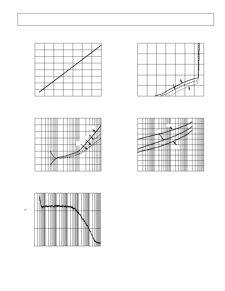
TYPICAL PERFORMANCE CHARACTERISTICS
1.310
1.305
1.300
1.295
1.290
1.285
1.280
1.275
1.270
50
125
100
75
50
25
0
25
05
74
9-
0
02
R
E
VE
R
S
E VO
L
T
A
G
E (V
)
TEMPERATURE (°C)
Figure 2. Output Drift for Different Temperature Characteristics
6
5
4
3
2
1
0
1
2
0.01
10
1
0.1
05
74
9-
0
03
O
UT
P
UT
V
O
L
T
A
G
E
E
RRO
R (
m
V
)
REVERSE CURRENT (mA)
+125°C
+85°C
+25°C
40°C
Figure 3. Output Voltage Error vs. Reverse Current
1000
100
10
1
1
1000000
100
1000
10000
100000
10
05
74
9-
0
04
N
O
I
S
E VO
L
T
A
G
E (
n
V/
H
z
)
FREQUENCY (Hz)
Figure 4. Noise Spectral Density
100
80
60
40
20
0
0
0.2
0.4
0.6
0.8
1.0
1.2
1.4
05
74
9-
0
05
RE
V
E
RS
E
CURRE
N
T
(
µ
A)
REVERSE VOLTAGE (V)
+85°C
+25°C
40°C
Figure 5. Reverse Current vs. Reverse Voltage
1.0
0.9
0.8
0.7
0.6
0.5
0.4
0.3
0.2
0.1
0
0.01
100
1
10
0.1
05
74
9-
0
06
F
O
RW
AR
D V
O
L
T
AG
E
(
V
)
FORWARD CURRENT (mA)
40°C
+85°C
+25°C
Figure 6. Forward Voltage vs. Forward Current
ADR1500
Rev. 0 | Page 6 of 8
THEORY OF OPERATION
The ADR1500 uses the band gap concept to produce a stable
voltage reference suitable for high accuracy data acquisition
components and systems. This device makes use of the underlying
physical nature of the silicon transistor base emitter voltage in
the forward-biased operating region. All such transistors have
an approximate -2 mV/°C temperature coefficient, which is not
suitable for use as a low TC reference; however, extrapolation of
the temperature characteristic of any one of these devices to
absolute zero (with collector current proportional to absolute
temperature) reveals that V
BE
goes to approximately the silicon
band gap voltage. Therefore, if a voltage could be developed
with an opposing temperature coefficient to the sum with the
V
BE
, than a zero TC reference would result. The ADR1500
circuit in Figure 7 provides such a compensating voltage, V1,
by deriving two transistors at different current densities and
amplifying the resultant V
BE
difference (V
BE
, which has a
positive TC). The sum of the V
BE
and V1 provides a stable
voltage reference.
057
49
-
00
8
V+
V
+
V
BE
V
BE
+
V1
+
Figure 7. Schematic Diagram
APPLYING THE ADR1500
The ADR1500 is simple to use in virtually all applications. To
operate the ADR1500 as a conventional shunt reference, see
Figure 8. An external series resistor is connected between the
supply voltage and the ADR1500.
For a given supply voltage, the series resistor, R
S
, determines the
reverse current flowing through the ADR1500. The value of R
S
must be chosen to accommodate the expected variations of the
supply voltage, V
S
, load current, I
L
, and the ADR1500 reverse
voltage, V
R
, while maintaining an acceptable reverse current, I
R
,
through the ADR1500.
The minimum value for R
S
should be enough to limit I
R
to
10 mA when V
S
is at its maximum, and I
L
and V
R
are at their
minimum. The equation for selecting R
S
is
)
(
)
(
L
R
R
S
S
I
I
V
V
R
+
-
=
05
74
9
-
00
9
(A)
R
S
V
S
V
R
I
R
+ I
L
V
OUT
I
R
+
I
L
(B)
R
S
+5V (+3V) ±10%
V
R
2.94k
(1.30k)
V
OUT
+
Figure 8. Typical Connection Diagram
Figure 8 shows a typical connection of the ADR1500 operating
at a minimum of 100 A. This connection can provide ±1 mA
to the load, while accommodating ±10% power supply
variations.
TURN-ON TIME
The turn-on time is a critical parameter for applications
demanding a large amount of processing. Figure 9 shows
the turn-on characteristics of the ADR1500.
0
574
9-
0
10
250mV/DIV
5µs/DIV
2.4V
0V
V
IN
C
L
= 200pF
Figure 9. Response Time
Upon application of power (cold start), the time required for
the output voltage to reach its final value within a specified
error is the turn-on settling time. Tow components are normally
associated with the time for active circuits to settle and the time
for the thermal gradients on the chip to stabilize. This characteristic
is generated from cold start operation and represents the true
turn-on waveform after power up. Figure 10 shows both the
course and fine turn-on settling characteristics of the device;
the total settling time to within 1.0 mV is about 6 s, and there
is no long thermal tail when the horizontal scale is expanded to
2 s/DIV. The output turn-on time is modified when an
external noise reduction filter is used. When present, the time
constant of the filter dominates the overall settling.
ADR1500
Rev. 0 | Page 7 of 8
0
574
9-
0
11
OUTPUT ERROR
1mV/DIV 2µs/DIV
OUTPUT
0.5mV/DIV 2ms/DIV
2.4V
0V
V
IN
Figure 10. Turn-On Settling Time
Attempts to drive a large capacitive load (in excess of 1000 pF)
can result in ringing. This is due to the additional poles formed
by the load capacitance and the output impedance of the reference.
A recommended method for driving capacitive loads of this
magnitude is shown in Figure 11.
057
49
-
012
+
V
R
V
OUT
C
L
R
S
= 11.5k
V
IN
R
L
Figure 11. Turn-On, Settling, and Transient Test Circuit
TRANSIENT RESPONSE
Many ADCs and DACs present transient current loads to the
reference. Poor reference response can degrade the converter's
performance. Figure 12 displays both the coarse and fine
settling characteristics of the device to load transient of ±50 A.
It shows the settling characteristics of the device for an
increased reverse current of 50 A and the response when the
reverse current is decreased by 50 A. The transients settle to
1 mV in about 3 s.
0
574
9-
0
13
I
R
= 100µA + 50µA STEP
I
R
= 100µA 50µA STEP
1µs/DIV
20mV/DIV
1mV/DIV
20mV/DIV
1mV/DIV
Figure 12. Transient Settling Time
A resistor isolates the capacitive load from the output stage,
while the capacitor provides a single-pole, low-pass filter and
lowers the output noise.
ADR1500
Rev. 0 | Page 8 of 8
OUTLINE DIMENSIONS
ALL DIMENSIONS COMPLIANT WITH EIAJ SC70
0.40
0.25
0.10 MAX
1.00
0.80
SEATING
PLANE
1.10
0.80
0.40
0.10
0.26
0.10
0.30
0.20
0.10
2
1
3
PIN 1
0.65 BSC
2.20
2.00
1.80
2.40
2.10
1.80
1.35
1.25
1.15
0.10 COPLANARITY
1
1
15
05
-
0
Figure 13. 3-Lead Thin Shrink Small Outline Transistor Package [SC70]
(KS-3)
Dimensions shown in millimeters
ORDERING GUIDE
Model
Initial Output Error
Temperature
Coefficient (Typ)
Temperature Range
Package
Description
Package
Option Branding
ADR1500BKSZ-REEL
1
2.6 mV
170 ppm/°C
-40°C to +85°C
3-Lead SC70
KS-3
R2F
1
Z = Pb-free part.
©2006 Analog Devices, Inc. All rights reserved. Trademarks and
registered trademarks are the property of their respective owners.
D05749-0-1/06(0)
Document Outline
- þÿ
- þÿ
- þÿ
- PIN CONFIGURATION
- þÿ
- þÿ
- þÿ
- þÿ
- þÿ
- þÿ
- þÿ