ƒÓÍÛÏÂÌÚýˆËˇ Ë ÓÔËÒýÌˡ www.docs.chipfind.ru
REV. A
ADR370
*
Precision Low Power 2.048 V
SOT-23 Voltage Reference
Information furnished by Analog Devices is believed to be accurate and
reliable. However, no responsibility is assumed by Analog Devices for its
use, nor for any infringements of patents or other rights of third parties that
may result from its use. No license is granted by implication or otherwise
under any patent or patent rights of Analog Devices. Trademarks and
registered trademarks are the property of their respective companies.
One Technology Way, P.O. Box 9106, Norwood, MA 02062-9106, U.S.A.
Tel: 781/329-4700
www.analog.com
Fax: 781/326-8703
© 2003 Analog Devices, Inc. All rights reserved.
*Protected by U.S.Patent No. 5,969,657; other patents pending.
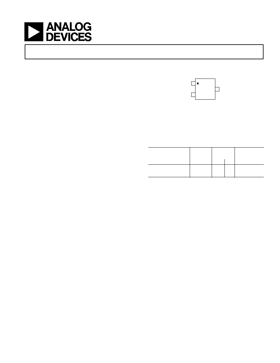
PIN CONFIGURATION
3-Lead SOT-23
1
3
2
V
IN
V
OUT
ADR370
GND
Table I. ADR370 Products
Output Initial
Temperature
Voltage Accuracy Coefficent
Products
(V
O
)
(mV)
(%) (ppm/
∞C)
ADR370BRT-REEL7
2.048
4 0.2 50
ADR370ART-REEL7
2.048
10 0.5 100
FEATURES
Initial Accuracy: 4 mV Max
Initial Accuracy Error: 0.2%
Low TCVO: 50 ppm/ C Max from ≠40 C to +125 C,
30 ppm/ C Max from +25 C to +70 C
Load Regulation: 200 V/mA, 100 ppm/mA
Line Regulation: 25 V/V, 20 ppm/V
Wide Operating Range: V
IN
= 2.3 V to 15 V
Low Power: 72 A Max
High Output Sink/Source Current: 5 mA Min
Wide Temperature Range: ≠40 C to +125 C
Tiny 3-Lead SOT-23 Package with Standard Pinout
APPLICATIONS
Battery-Powered Instrumentation
Portable Medical Instruments
Data Acquisition Systems
Industrial Process Control Systems
Automotive
GENERAL DESCRIPTION
The ADR370 is a low cost, 3-terminal (series) band-gap voltage
reference featuring high accuracy, high stability, and low power
consumption packaged in a tiny 3-lead SOT-23 package. Precise
matching and thermal tracking of on-chip components, as well as
patented temperature drift curvature correction design techniques,
have been employed to ensure that the ADR370 provides an
accurate 2.048 V output.
This micropowered, low dropout voltage device will source or
sink up to 5 mA of load current while providing a stable 2.048 V
output. The compact footprint, high accuracy, and an operating
range of 2.3 V to 12 V make the ADR370 ideal for use in 3 V
and 5 V systems where there may be wide variations in supply
voltage and a need to minimize power dissipation.
The ADR370 is offered in A and B grades; all devices are specified
over the extended industrial range of ≠40
∞C to +125∞C.
REV. A
≠2≠
ADR370≠SPECIFICATIONS
ELECTRICAL CHARACTERISTICS
Parameter
Symbol
Conditions
Min
Typ
Max
Unit
Output Voltage (@ 25
∞C)
V
O
2.044
2.048 2.052
V
Initial Accuracy Error
A Grade
V
OERR
≠10
+10
mV
V
OERR
≠0.5
+0.5
%
B Grade
V
OERR
≠4
+4
mV
V
OERR
≠0.2
+0.2
%
Output Voltage Temperature Drift
A Grade
TCV
O
≠40
∞C to +125∞C
100
ppm/
∞C
B Grade
TCV
O
≠40
∞C to +125∞C
50
ppm/
∞C
TCV
O
25
∞C to 70∞C
30
ppm/
∞C
Supply Headroom
V
IN
≠ V
OUT
200
mV
Load Regulation
0 mA < I
OUT
< 5 mA @ 25
∞C
≠0.200
+0.200
mV/mA
≠3 mA < I
OUT
< 0 mA @ 25
∞C
≠0.480
+0.480
mV/mA
≠0.1 mA < I
OUT
< +0.1 mA
≠0.425
+0.425
mV/mA
Line Regulation
V
OUT
200 mV < V
IN
< 15 V
20
ppm/V
I
OUT
= 0 mA
Ripple Rejection
V
OUT
/
V
IN
V
IN
= 5 V
± 100 mV (f = 120 Hz)
80
dB
Quiescent Current
72
µA
Short-Circuit Current to Ground
15
µA
Noise Voltage (@ 25
∞C)
0.1 Hz to 10 Hz
70
µV p-p
10 Hz to 10 kHz
50
µV rms
Turn-On Settling Time
C
L
= 0.2
µF
100
µs
Long Term Stability
1,000 Hours @ 25
∞C
100
ppm/1,000 hrs
Output Voltage Hysteresis
115
ppm
Temperature Range
≠40
+125
∞C
*Guaranteed by characterization.
Specifications subject to change without notice.
(T
A
= T
MIN
to T
MAX
, V
IN
= 5 V, unless otherwise noted.)
REV. A
ADR370
≠3≠
ABSOLUTE MAXIMUM RATINGS
*
Supply Voltage . . . . . . . . . . . . . . . . . . . . . . . . . . . . . . . . . . 18 V
Storage Temperature Range
RT Package . . . . . . . . . . . . . . . . . . . . . . . . ≠65
∞C to +125∞C
Operating Temperature Range . . . . . . . . . . . ≠40
∞C to +125∞C
Lead Temperature Range
Soldering, 60 sec . . . . . . . . . . . . . . . . . . . . . . . . . . . . 215
∞C
Infrared, 15 sec . . . . . . . . . . . . . . . . . . . . . . . . . . . . . 220
∞C
*Absolute maximum ratings apply at 25
∞C, unless otherwise noted.
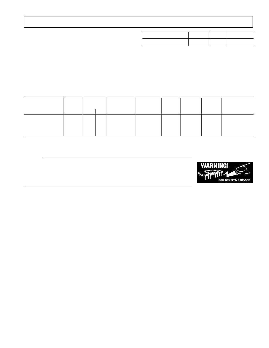
CAUTION
ESD (electrostatic discharge) sensitive device. Electrostatic charges as high as 4000 V readily
accumulate on the human body and test equipment and can discharge without detection. Although the
ADR370 features proprietary ESD protection circuitry, permanent damage may occur on devices
subjected to high energy electrostatic discharges. Therefore, proper ESD precautions are recommended
to avoid performance degradation or loss of functionality.
ORDERING GUIDE
Output
Initial
Temperature
Number
Voltage
Accuracy
Coefficient
Package
Package
of Parts
Temperature
Model
(V
O
)
(mV) (%)
(ppm/
∞C)
Description
Option
Branding per Reel
Range
ADR370BRT-R2
2.048
±4 0.5
50
SOT-23
3-Lead
RPB
250
≠40
∞C to +125∞C
ADR370BRT-REEL7
2.048
±4 0.2
50
SOT-23
3-Lead
RPB
3,000
≠40
∞C to +125∞C
ADR370ART-R2
2.048
±10 0.5
100
SOT-23
3-Lead
RPA
250
≠40
∞C to +125∞C
ADR370ART-REEL7 2.048
±10 0.5
100
SOT-23
3-Lead
RPA
3,000
≠40
∞C to +125∞C
Package Type
JA
JC
Unit
3-SOT-23 (RT)
220
102
∞C/W
REV. A
≠4≠
ADR370≠Typical Performance Characteristics
LOAD ≠ mA
12
≠4
≠4
5
≠3
V
O ≠
mV
≠2
≠1
0
1
2
3
4
10
4
2
0
≠2
8
6
≠40 C
+125 C
+25 C
TPC 1. Load Regulation vs. Load Current
TEMPERATURE ≠ C
2.048
2.036
≠40
OUTPUT VOLTAGE ≠ V
45
125
2.038
2.040
2.042
2.044
2.046
V
IN
= 5V
V
IN
= 15V
TPC 2. Output Voltage vs. Temperature
TEMPERATURE ≠ C
80
20
≠40
SUPPLY CURRENT ≠
A
45
125
30
40
50
60
70
V
IN
= 5V
V
IN
= 15V
TPC 3. Supply Current vs. Temperature
TEMPERATURE ≠ C
6
≠10
≠40
LINE REGULATION ≠ ppm/V
45
125
≠8
0
4
V
IN
5V TO 15V
≠6
≠4
≠2
2
TPC 4. Line Regulation vs. Temperature
TIME ≠ 0.1s/DIV
0
0
0
0
0
0
VO
LTA
G
E
≠ 10
V/DIV
0
0
0
0
0
0
0
0
0
0
0
0
0
0
TPC 5. Voltage Noise 0.1 Hz to 10 Hz
TIME ≠ 0.1s/DIV
0
0
0
0
0
0
VO
LTA
G
E
≠ 200
V/DIV
0
0
0
0
0
0
0
0
0
0
0
0
0
0
TPC 6. Voltage Noise 10 Hz to 100 kHz
REV. A
ADR370
≠5≠
TIME ≠ 100 s/DIV
0
0
0
0
0
0
VO
LTA
G
E
≠
V
0
0
0
0
0
0
0
0
0
0
0
0
0
0
V
OUT
= 1V/DIV
V
IN
= 5V/DIV
C
BY
= 0.1 F
C
LOAD
= 0.22 F
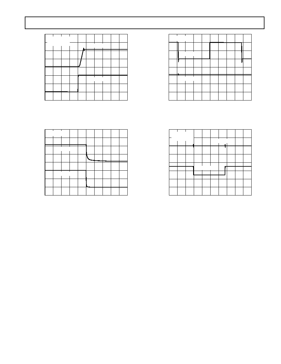
TPC 7. Turn-On Response
TIME ≠ 100 s/DIV
0
0
0
0
0
0
VO
LTA
G
E
≠
V
0
0
0
0
0
0
0
0
0
0
0
0
0
0
V
OUT
= 1V/DIV
V
IN
= 5V/DIV
R
LOAD
= 1k
TPC 8. Turn-Off Response
TIME ≠ 100 s/DIV
0
0
0
0
0
0
VO
LTA
G
E
≠
V
0
0
0
0
0
0
0
0
0
0
0
0
0
0
V
IN
= 1V/DIV
V
OUT
= 1V/DIV
C
L
= 0.1 F
TPC 9. Line Transient Response
TIME ≠ 100ms/DIV
0
0
0
0
0
0
VO
LTA
G
E
≠
V
0
0
0
0
0
0
0
0
0
0
0
0
0
0
V
OUT
= 20mV/DIV
V
IN
= 2V/DIV
C
BY
= 0.1 F
C
LOAD
= 0.1 F
TPC 10. Load Transient Response
REV. A
≠6≠
ADR370
PARAMETER DEFINITIONS
Temperature Coefficient
Temperature coefficient is the change of output voltage with
respect to operating temperature changes, normalized by the
output voltage at 25
∞C. This parameter is expressed in ppm/∞C
and can be determined with the following equation
TCV
ppm
C
V
T
V
T
V
C
T
T
O
O
O
O
∞
=
( )
-
( )
∞
(
)
◊
-
(
)
◊
2
1
2
1
6
25
10
(1)
where:
V
O
(25
∞C) = V
O
at 25
∞C.
V
O
(T
1
) = V
O
at Temperature 1.
V
O
(T
2
) = V
O
at Temperature 2.
Line Regulation
Line regulation is the change in output voltage due to a specified
change in input voltage. This parameter accounts for the effects
of self-heating. Line regulation is expressed in either percent per
volt, parts-per-million per volt, or microvolts per volt change in
input voltage.
Load Regulation
Load regulation is the change in output voltage due to a specified
change in load current. This parameter accounts for the effects
of self-heating. Load regulation is expressed in either microvolts
per milliampere, parts-per-million per milliampere, or ohms of
dc output resistance.
Long Term Stability
Long term stability is the typical shift of output voltage at 25
∞C
on a sample of parts subjected to a test of 1,000 hours at 25
∞C.
V
V
t
V
t
V
ppm
V
t
V
t
V
t
O
O
O
O
O
O
O
=
( )
-
( )
[ ]
=
( )
-
( )
( )
◊
0
1
0
1
0
6
10
(2)
where:
V
O
(T
1
) = V
O
at 25
∞C at time 0.
V
O
(T
2
) = V
O
at 25
∞C after 1,000 hours operation at 25∞C.
Thermal Hysteresis
Thermal hysteresis is defined as the change of output voltage after
the device is cycled through temperature from +25
∞C to ≠40∞C
to +125
∞C and back to +25∞C. This is a typical value from a sample
of parts put through such a cycle.
V
V
C
V
V
ppm
V
C
V
V
C
O
HYS
O
O TC
O
HYS
O
O TC
O
_
_
_
_
=
∞
(
)
-
[ ]
=
∞
(
)
-
∞
(
)
◊
25
25
25
10
6
(3)
where:
V
O
(25
∞C) = V
O
at 25
∞C.
V
O_TC
= V
O
at 25
∞C after temperature cycle at +25∞C to ≠40∞C
to +125
∞C and back to +25∞C.
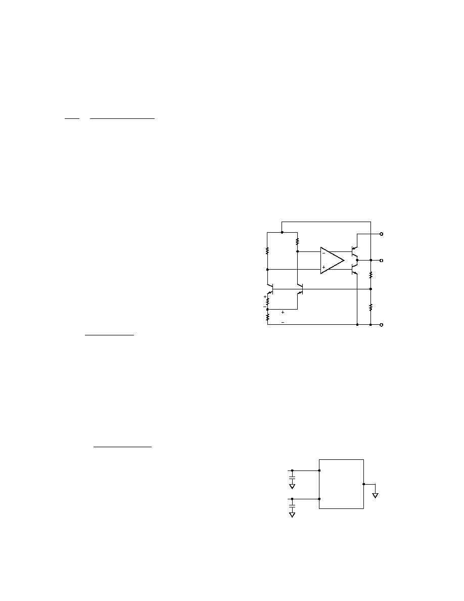
THEORY OF OPERATION
The ADR370 uses the band-gap concept to produce a stable,
low temperature coefficient voltage reference suitable for high
accuracy data acquisition components and systems. This device
makes use of underlying temperature characteristics of a silicon
transistor's base-emitter voltage (V
BE
) in the forward biased
operating region. Under this condition, all such transistors have
a ≠2 mV/
∞C temperature coefficient (TC) and a V
BE
that, when
extrapolated to absolute zero, 0 K, (with collector current pro-
portional to absolute temperature) approximates the silicon
band-gap voltage. By summing a voltage that has an equal and
opposite temperature coefficient of 2 mV/
∞C with a V
BE
of a
forward biased transistor, an almost zero TC reference can be
developed. The simplified circuit diagram in Figure 1 shows how
a compensating voltage, V1, is achieved by driving two transistors
at different current densities and amplifying the resultant V
BE
difference (
V
BE
, which has a positive TC). The sum (V
BG
) of V
BE
and V1 is then buffered and amplified to produce a stable reference
voltage of 2.048 V at the output.
V
IN
V
OUT
GND
V
DS
R5
R6
R4
R3
R2
R1
V1
Figure 1. Simplified Schematic
Applying the ADR370
In order to achieve the specified performance, two external
components should be used in conjunction with the ADR370,
a 4.7
µF capacitor and a 1 µF capacitor should be applied to the
input and output, respectively. Figure 2 shows the ADR370 with
both the input and output capacitors attached.
For further transient response optimization, an additional 0.1
µF
capacitor in parallel with the 4.7
µF input capacitor can be used.
A 1
µF output capacitor will provide stable performance for all
loading conditions. The ADR370 can, however, operate under
low (≠100
µA < I
OUT
< +100
µA) current conditions with just a
0.2
µF output capacitor and a 1 µF input capacitor.
C
IN
V
IN
ADR370
GND
4.7 F
C
OUT
V
OUT
1 F
Figure 2. Typical Connection Diagram
REV. A
ADR370
≠7≠
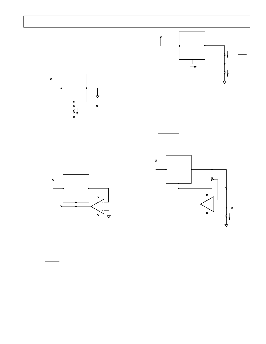
APPLICATIONS
Low Cost Negative Reference
A low cost negative reference can be obtained by leveraging the
current sinking capability of the ADR370. Simply tying the V
OUT
terminal to ground and adding a bias resistor, R
SET
, to the GND
pin of the device, a negative voltage reference can be obtained
as shown in Figure 3. R
SET
should be chosen such that I
SET
remains between 1 mA to 5 mA.
V
IN
V
DD
V
SS
R
SET
I
SET
ADR370
V
OUT
GND
≠VREF
Figure 3. Low Cost Negative Reference
Precision Negative Reference
Without using any matching resistors, a precision negative reference
can be obtained using the configuration shown in Figure 4. The
voltage difference between V
OUT
and GND of the ADR370 is
2.048 V. Since V
OUT
is at virtual ground, U2 will close the loop by
forcing the GND pin to be the negative reference node. U2 should
be a low offset voltage precision op amp, such as the OP1177.
V
IN
+15V
U2
U1
2.3V TO 12V
OP1177
≠15V
ADR370
V
OUT
GND
≠VREF
Figure 4. Precision Negative Reference
Low Cost Current Source
Figure 5 illustrates how a simple, low cost current source can be
configured using the ADR370. The load current, I
L
, is simply
the sum of I
SET
and the quiescent current, I
q
. I
SET
is simply the
reference voltage generated by the ADR370 divided by R
SET
.
I
V
R
SET
SET
=
2 048
.
(4)
The quiescent current, I
q
, varies slightly with load. The variation
in I
q
limits the use of this circuit to general-purpose applications.
V
IN
V
L
+ 2.5V < V
DD
< V
L
+ 12V
ADR370
V
OUT
GND
I
SET
=
R
SET
R
SET
V
L
R
L
I
L
I
q
= 65 A
2.048V
Figure 5. Low Cost Current Source
Precision Current Source with Adjustable Output
A precision current source can be implemented with the circuit
shown in Figure 6. By adding a mechanical or digital potenti-
ometer, this circuit becomes an adjustable current source. If a
digital potentiometer like the AD5201 is used, the load current
is simply the voltage across terminals B-to-W of the digital
potentiometer divided by R
SET
.
I
V
D
R
L
REF
SET
=
◊
◊ 256
(5)
where D is the decimal equivalent of the digital potentiometer
input code.
V
IN
+12V
A
B
W
≠2.048V TO V
L
0V TO (2.048V + V
L
)
12V
OP1177
AD5201
≠12V
ADR370
V
OUT
GND
V
L
R
L
R
SET
I
L
Figure 6. Programmable 0 mA to 5 mA Current Source
To optimize the resolution of this circuit, dual supply op amps
should be used because the ground potential of ADR370 can
swing from ≠2.048 V at zero scale to V
L
at full scale of the
potentiometer setting.
REV. A
≠8≠
ADR370
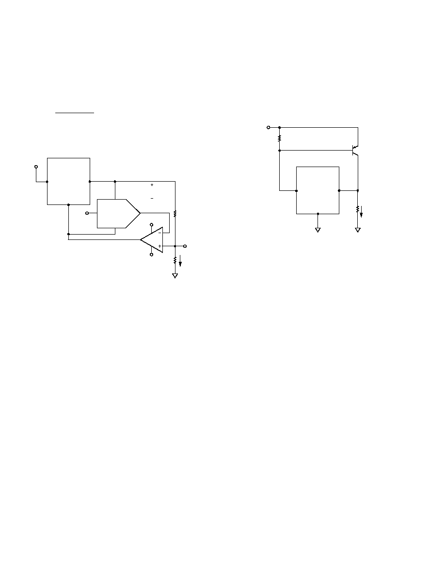
12-Bit Precision Programmable Current Source
By replacing the potentiometer in Figure 6 with a 12-bit precision
DAC like the AD5322, a higher precision programmable current
source can be achieved. Figure 7 illustrates the implementation
of this circuit. The load current can be determined with the
following equation.
I
V
D
R
L
REF
SET
=
-
(
)
◊
1
4096
(6)
The compliance voltage should be kept low so that the supply
voltage to U2, between V
DD
and GND, does not fall below 2.5 V.
V
IN
U1
U2
+5V
V+
V≠
1
11
U3
2
3
VREF (1 ≠ D2/N)
+5V
OP1177
AD5322
≠5V
ADR370
V
OUT
GND
+5V
V
L
R
L
R
SET
TOL
±0.05%
I
L
V
IN
V
DD
V
O
GND
Figure 7. 12-Bit Programmable Current Source
Precision Boosted Output Regulator
A precision voltage output with boosted current can be realized
with the circuit shown in Figure 8. In this circuit, V
O
is maintained
by the ADR370 at 2.048 V.
The ADR370 sources a maximum of 5 mA if the load current,
I
L
, is more than 5 mA, current is furnished by the transistor, Q1,
and the input voltage supply V
DD
.
V
IN
R1
10k
R
L
I
L
ADR370
V
OUT
GND
V
DD
Q1
2N3906
4V TO 12V
Figure 8. Precision Boosted Output Regulator
Q1 will be turned on to regulate current as needed. R1 is required
to bias the base of Q1 and must be large enough to comply with
the supply current requirements of the ADR370. The supply
voltage can be as low as 4 V.
The maximum current output of this circuit is limited by the
power dissipation of the bipolar transistor, Q1.
P
V
I
DISS
DD
L
=
-
(
)
◊
2 048
.
(7)
Using the 2N3906 PNP transistor shown in Figure 8 and a 4 V
power supply, R
L
should be chosen so that a maximum of 100 mA
is drawn from the circuit, which limits the power dissipation of
Q1 to ~200 mW.
REV. A
ADR370
≠9≠
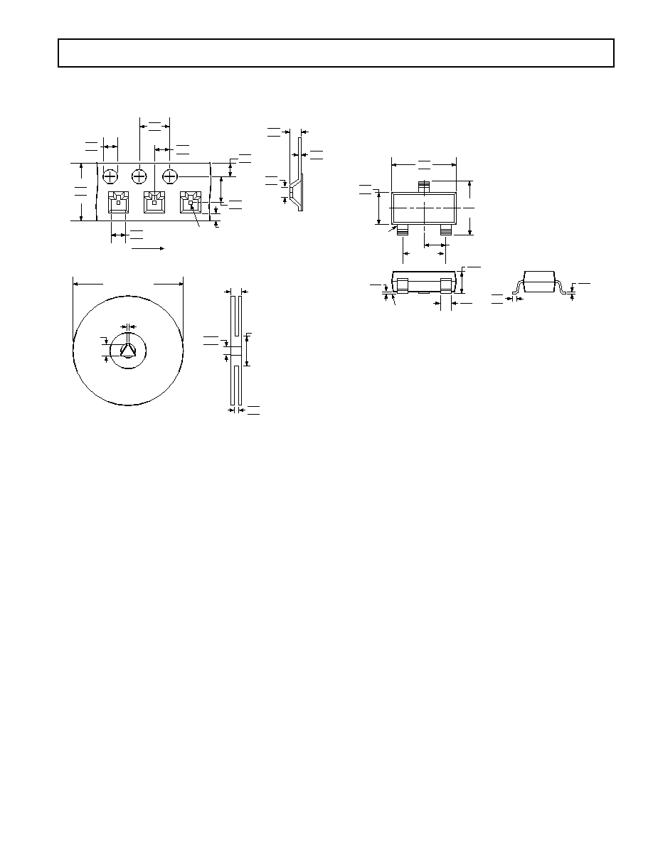
TAPE AND REEL DIMENSIONS
Dimensions shown in millimeters.
2.80
2.70
2.60
1.10
1.00
0.90
0.35
0.30
0.25
4.10
4.00
3.90
1.55
1.50
1.50
8.30
8.00
7.70
3.20
3.10
2.90
2.05
2.00
1.95
1.85
1.75
1.65
3.55
3.50
3.45
0.75 MIN
DIRECTION OF UNREELING
1.00 MIN
13.20
13.00
12.80
9.90
8.40
8.40
20.20
MIN
1.50 MIN
7" REEL 100.00
OR
13" REEL 330.00
7" REEL 50.00 MIN
OR
13" REEL 100.00 MIN
14.40 MAX
OUTLINE DIMENSIONS
3-Lead Small Outline Transistor Package [SOT-23-3]
(RT-3)
Dimensions shown in millimeters.
3.04
2.90
2.80
PIN 1
1.40
1.30
1.20
2.64
2.10
1.90 BSC
1
2
3
SEATING
PLANE
1.12
0.89
0.10
0.01
0.50
0.30
0.20
0.08
0.60
0.50
0.40
0.95 BSC
COMPLIANT TO JEDEC STANDARDS TO-236AB

REV. A
≠10≠
ADR370
Revision History
Location
Page
7/03--Data Sheet changed from REV. 0 to REV. A.
Updated FEATURES . . . . . . . . . . . . . . . . . . . . . . . . . . . . . . . . . . . . . . . . . . . . . . . . . . . . . . . . . . . . . . . . . . . . . . . . . . . . . . . . . . . . 1
Updated Table I . . . . . . . . . . . . . . . . . . . . . . . . . . . . . . . . . . . . . . . . . . . . . . . . . . . . . . . . . . . . . . . . . . . . . . . . . . . . . . . . . . . . . . . . 1
Updated ELECTRICAL CHARACTERISTICS . . . . . . . . . . . . . . . . . . . . . . . . . . . . . . . . . . . . . . . . . . . . . . . . . . . . . . . . . . . . . . . 2
Updated ABSOLUTE MAXIMUM RATINGS . . . . . . . . . . . . . . . . . . . . . . . . . . . . . . . . . . . . . . . . . . . . . . . . . . . . . . . . . . . . . . . . 3
Updated ORDERING GUIDE . . . . . . . . . . . . . . . . . . . . . . . . . . . . . . . . . . . . . . . . . . . . . . . . . . . . . . . . . . . . . . . . . . . . . . . . . . . . . 3
Updated PARAMETER DEFINITIONS . . . . . . . . . . . . . . . . . . . . . . . . . . . . . . . . . . . . . . . . . . . . . . . . . . . . . . . . . . . . . . . . . . . . . 6
Updated OUTLINE DIMENSIONS . . . . . . . . . . . . . . . . . . . . . . . . . . . . . . . . . . . . . . . . . . . . . . . . . . . . . . . . . . . . . . . . . . . . . . . . 9

≠11≠

C03432≠0≠7/03(A)
≠12≠
Document Outline
- FEATURES
- APPLICATIONS
- GENERAL DESCRIPTION
- PIN CONFIGURATION
- SPECIFICATIONS
- ABSOLUTE MAXIMUM RATINGS
- ORDERING GUIDE
- TYPICAL PERFORMANCE CHARACTERISTICS
- PARAMETER DEFINITIONS
- Temperature Coefficient
- Line Regulation
- Load Regulation
- Long Term Stability
- Thermal Hysteresis
- THEORY OF OPERATION
- APPLICATIONS
- Low Cost Negative Reference
- Precision Negative Reference
- Low Cost Current Source
- Precision Current Source with Adjustable Output
- 12-Bit Precision Programmable Current Source
- Precision Boosted Output Regulator
- TAPE AND REEL DIMENSIONS
- OUTLINE DIMENSIONS
- REVISION HISTORY