/home/web/htmldatasheet/RUSSIAN/html/ad/164576
REV. A
Information furnished by Analog Devices is believed to be accurate and
reliable. However, no responsibility is assumed by Analog Devices for its
use, nor for any infringements of patents or other rights of third parties
which may result from its use. No license is granted by implication or
otherwise under any patent or patent rights of Analog Devices.
a
One Technology Way, P.O. Box 9106, Norwood, MA 02062-9106, U.S.A.
Tel: 781/329-4700
World Wide Web Site: www.analog.com
Fax: 781/326-8703
© Analog Devices, Inc., 2001
ADR390/ADR391
Precision Low Drift 2.048 V/2.500 V
SOT-23 Voltage References with Shutdown
FEATURES
Load Regulation: 60 ppm/mA
Line Regulation: 25 ppm/V
Wide Operating Range:
2.4 V18 V for ADR390
2.8 V18 V for ADR391
Low Power: 120 A Max
Shutdown to Less than 3 A Max
High Output Current: 5 mA Min
Wide Temperature Range: 40 C to +85 C
Tiny SOT-23-5 Package
APPLICATIONS
Battery-Powered Instrumentation
Portable Medical Instruments
Data Acquisition Systems
Industrial and Process Control Systems
Hard Disk Drives
Automotive
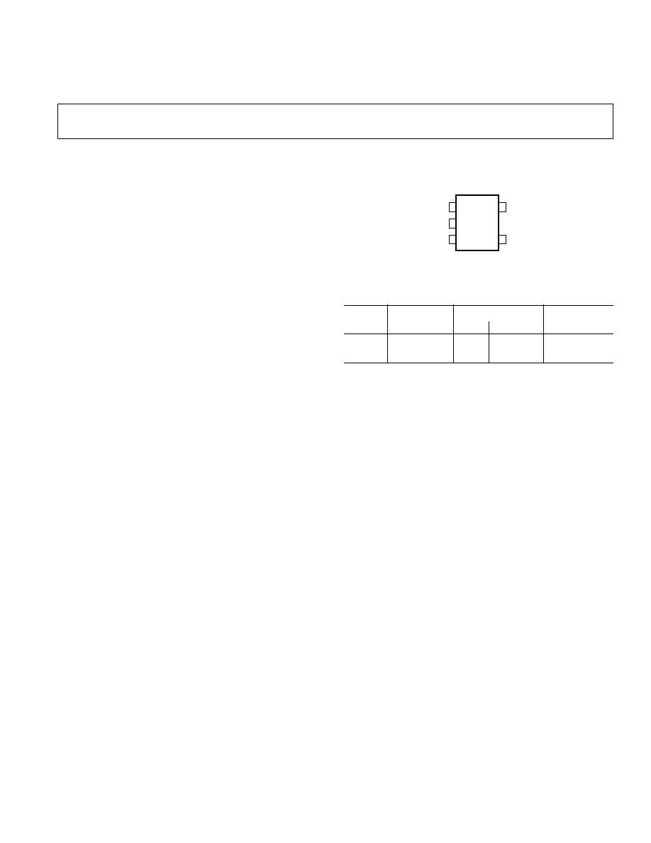
PIN CONFIGURATION
5-Lead SOT-23
(RT Suffix)
1
2
3
ADR390/
ADR391
(Not to Scale)
5
4
SHDN
V
IN
V
OUT (SENSE)
GND
V
OUT (FORCE)
Table I. ADR39x Products
Part
Output
Initial Accuracy
Tempco
Number
Voltage (V)
mV
%
ppm/ C, Max
ADR390
2.048
±6
±0.29
25
ADR391
2.500
±6
±0.24
25
GENERAL DESCRIPTION
The ADR390 and ADR391 are precision 2.048 V and 2.5 V
bandgap voltage references featuring high accuracy and stability
and low power consumption in a tiny footprint. Patented temperature
drift curvature correction techniques minimize nonlinearity of the
voltage change with temperature. The wide operating range and
low power consumption with additional shutdown capability
make them ideal for 3 V to 5 V battery-powered applications.
The V
OUT
Sense Pin enables greater accuracy by supporting full
Kelvin operation in systems using very fine or long circuit traces.
The ADR390 and ADR391 are micropower, Low Dropout Voltage
(LDV) devices that provide a stable output voltage from supplies as
low as 300 mV above the output voltage. They are specified over the
industrial (40
°C to +85°C) temperature range. Each is available
in the tiny 5-lead SOT-23 package.
The combination of V
OUT
sense and shutdown functions also
enables a number of unique applications combining precision
reference/regulation with fault decision and overcurrent protec-
tion. Details are provided in the Applications section.
REV. A
2
ADR390/ADR391
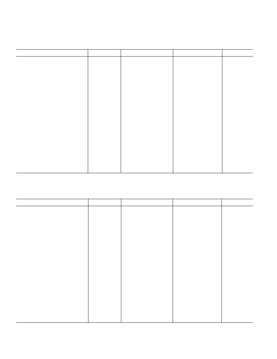
ELECTRICAL CHARACTERISTICS
Parameter
Symbol
Conditions
Min
Typ
Max
Unit
Output Voltage
V
O
2.042
2.048 2.054
V
Initial Accuracy
V
OERR
6
+6
mV
0.29
+0.29
%
Temperature Coefficient
TCV
O
40
°C < T
A
< +85
°C
5
25
ppm/
°C
0
°C < T
A
< 70
°C
3
21
ppm/
°C
Minimum Supply Voltage Headroom
V
IN
V
O
I
L
3 mA
300
mV
Line Regulation
V
O
/
V
IN
V
IN
= 2.5 V to 15 V
40
°C < T
A
< +85
°C
10
25
ppm/V
Load Regulation
V
O
/
I
LOAD
V
IN
= 3 V,
I
LOAD
= 0 mA to 5 mA
40
°C < T
A
< +85
°C
60
ppm/mA
Quiescent Current
I
IN
No Load
100
120
µA
40
°C < T
A
< +85
°C
140
µA
Voltage Noise
e
N
0.1 Hz to 10 Hz
5
µV p-p
Turn-On Settling Time
t
R
20
µs
Long-Term Stability
V
O
See Figure 1
50
ppm
Output Voltage Hysteresis
V
O_HYS
40
ppm
Ripple Rejection Ratio
RRR
f
IN
= 60 Hz
85
dB
Short Circuit to GND
I
SC
30
mA
Shutdown Supply Current
I
SHDN
3
µA
Shutdown Logic Input Current
I
LOGIC
500
nA
Shutdown Logic Low
V
INL
0.8
V
Shutdown Logic High
V
INH
2.4
V
Specifications subject to change without notice.
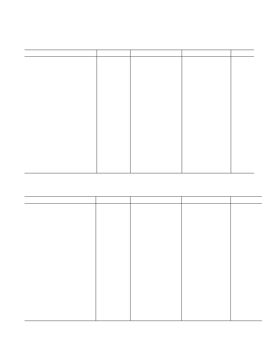
(@ V
IN
= 5 V, T
A
= 25 C unless otherwise noted.)
(@ V
IN
= 15 V, T
A
= 25 C unless otherwise noted.)
ADR390 SPECIFICATIONS
REV. A
3
ADR390/ADR391
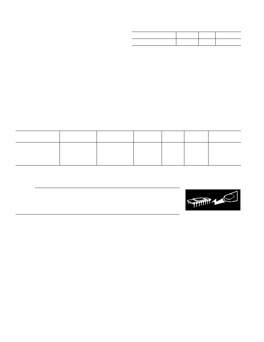
ELECTRICAL CHARACTERISTICS
Parameter
Symbol
Conditions
Min
Typ
Max
Unit
Output Voltage
V
O
2.494
2.5
2.506
V
Initial Accuracy
V
OERR
6
+6
mV
0.24
+0.24
%
Temperature Coefficient
TCV
O
40
°C < T
A
< +85
°C
5
25
ppm/
°C
0
°C < T
A
< 70
°C
3
21
ppm/
°C
Minimum Supply Voltage Headroom
V
IN
V
O
I
L
2 mA
300
mV
Line Regulation
V
O
/
V
IN
V
IN
= 2.8 V to 15 V
40
°C < T
A
< +85
°C
10
25
ppm/V
Load Regulation
V
O
/
I
LOAD
V
IN
= 3.5 V,
I
LOAD
= 0 mA to 5 mA
40
°C < T
A
< +85
°C
60
ppm/mA
Quiescent Current
I
IN
No Load
100
120
µA
40
°C < T
A
< +85
°C
140
µA
Voltage Noise
e
N
0.1 Hz to 10 Hz
5
µV p-p
Turn-On Settling Time
t
R
20
µs
Long-Term Stability
V
O
See Figure 1
50
ppm
Output Voltage Hysteresis
V
O_HYS
75
ppm
Ripple Rejection Ratio
RRR
f
IN
= 60 Hz
85
dB
Short Circuit to GND
I
SC
25
mA
Shutdown Supply Current
I
SHDN
3
µA
Shutdown Logic Input Current
I
LOGIC
500
nA
Shutdown Logic Low
V
INL
0.8
V
Shutdown Logic High
V
INH
2.4
V
Specifications subject to change without notice.
ELECTRICAL CHARACTERISTICS
Parameter
Symbol
Conditions
Min
Typ
Max
Unit
Output Voltage
V
O
2.494
2.5
2.506
V
Initial Accuracy
V
OERR
6
+6
mV
0.24
+0.24
%
Temperature Coefficient
TCV
O
40
°C < T
A
< +85
°C
5
25
ppm/
°C
0
°C < T
A
< 70
°C
3
21
ppm/
°C
Minimum Supply Voltage Headroom
V
IN
V
O
I
L
2 mA
300
mV
Line Regulation
V
O
/
V
IN
V
IN
= 2.8 V to 15 V
40
°C < T
A
< +85
°C
10
25
ppm/V
Load Regulation
V
O
/
I
LOAD
V
IN
= 3.5 V,
I
LOAD
= 0 mA to 5 mA
40
°C < T
A
< +85
°C
60
ppm/mA
Quiescent Current
I
IN
No Load
100
120
µA
40
°C < T
A
< +85
°C
140
µA
Voltage Noise
e
N
0.1 Hz to 10 Hz
5
µV p-p
Turn-On Settling Time
t
R
20
µs
Long-Term Stability
V
O
See Figure 1
50
ppm
Output Voltage Hysteresis
V
O_HYS
75
ppm
Ripple Rejection Ratio
RRR
f
IN
= 60 Hz
85
dB
Short Circuit to GND
I
SC
30
mA
Shutdown Supply Current
I
SHDN
3
µA
Shutdown Logic Input Current
I
LOGIC
500
nA
Shutdown Logic Low
V
INL
0.8
V
Shutdown Logic High
V
INH
2.4
V
Specifications subject to change without notice.
(@ V
IN
= 5 V, T
A
= 25 C unless otherwise noted).
(@ V
IN
= 15 V, T
A
= 25 C unless otherwise noted.)
ADR391 SPECIFICATIONS
REV. A
4
ADR390/ADR391
ABSOLUTE MAXIMUM RATINGS
*
Supply Voltage . . . . . . . . . . . . . . . . . . . . . . . . . . . . . . . . . 18 V
Shutdown Logic Level . . . . . . . . . . . . . . . . . . . . . . . . . . . 18 V
Or Supply Voltage, Whichever is Lower . . . . . . . . . . . . 18 V
Output Short-Circuit Duration to GND . . . . . . . . . . Indefinite
Storage Temperature Range
RT Package . . . . . . . . . . . . . . . . . . . . . . . 65
°C to +150°C
Operating Temperature Range
ADR390/ADR391 . . . . . . . . . . . . . . . . . . 40
°C to +85°C
Junction Temperature Range
RT Package . . . . . . . . . . . . . . . . . . . . . . . 65
°C to +150°C
Lead Temperature Range (Soldering, 60 sec) . . . . . . . 300
°C
*Stresses above those listed under Absolute Maximum Ratings may cause perma-
nent damage to the device. This is a stress rating only; functional operation of the
device at these or any other conditions above those listed in the operational sections
of this specification is not implied. Exposure to absolute maximum rating condi-
tions for extended periods may affect device reliability.
Package Type
JA
*
JC
Unit
5-Lead SOT-23 (RT)
230
°C/W
*
JA
is specified for worst-case conditions, i.e.,
JA
is specified for device in
socket for SOT packages.
ORDERING GUIDE
Temperature
Package
Package
Top
Output
Number of
Model
Range
Description
Option
Mark
Voltage
Parts Per Reel
ADR390ARTREEL7
40 C to +85 C
5-Lead SOT
RT-5
R0A
2.048
3,000
ADR390ARTREEL
40 C to +85 C
5-Lead SOT
RT-5
R0A
2.048
10,000
ADR391ARTREEL7
40 C to +85 C
5-Lead SOT
RT-5
R1A
2.500
3,000
ADR391ARTREEL
40 C to +85 C
5-Lead SOT
RT-5
R1A
2.500
10,000
CAUTION
ESD (electrostatic discharge) sensitive device. Electrostatic charges as high as 4000 V readily
accumulate on the human body and test equipment and can discharge without detection. Although
the ADR390/ADR391 features proprietary ESD protection circuitry, permanent damage may
occur on devices subjected to high-energy electrostatic discharges. Therefore, proper ESD
precautions are recommended to avoid performance degradation or loss of functionality.
WARNING!
ESD SENSITIVE DEVICE
REV. A
ADR390/ADR391
5
PARAMETER DEFINITION
Temperature Coefficient (TCV
O
)
The change of output voltage over the operating temperature
change and normalized by the output voltage at 25 C, expressed
in ppm/ C. The equation follows:
TCV
ppm C
V
T
V
T
V
C
T
T
O
O
O
O
°
]
[
=
( )
-
( )
°
( )
×
-
(
)
×
2
1
2
1
6
25
10
Where:
V
O
(25 C) = V
O
at 25 C.
V
O
(T
1
) = V
O
at temperature1.
V
O
(T
2
) = V
O
at temperature2.
Line Regulation (
V
O
/
V
IN
)
The change in output voltage due to a specified change in input
voltage. It includes the effects of self-heating. Line regulation is
expressed in either percent per volt, parts-per-million per volt,
or microvolts per volt change in input voltage.
Load Regulation (
V
O
/
I
LOAD
)
The change in output voltage due to a specified change in load
current. It includes the effects of self-heating. Load Regulation
is expressed in either microvolts per milliampere, parts-per-million
per milliampere, or
of dc output resistance.
Input Capacitor
Input capacitors are not required on the ADR390/ADR391. There
is no limit for the value of the capacitor used on the input,
but a 1
µF to 10 µF capacitor on the input will improve transient
response in applications where the supply suddenly changes. An
additional 0.1
µF in parallel will also help reducing noise from
the supply.
Output Capacitor
The ADR390/ADR391 does not need output capacitors for
stability under any load condition. An output capacitor, typi-
cally 0.1
µF, will filter out any low-level noise voltage and will
not affect the operation of the part. On the other hand, the load
transient response can be improved with an additional 1
µF to
10
µF output capacitor in parallel. A capacitor here will act as a
source of stored energy for sudden increase in load current. The
only parameter that will degrade, by adding an output capacitor,
is turn-on time and it depends on the size of the capacitor chosen.
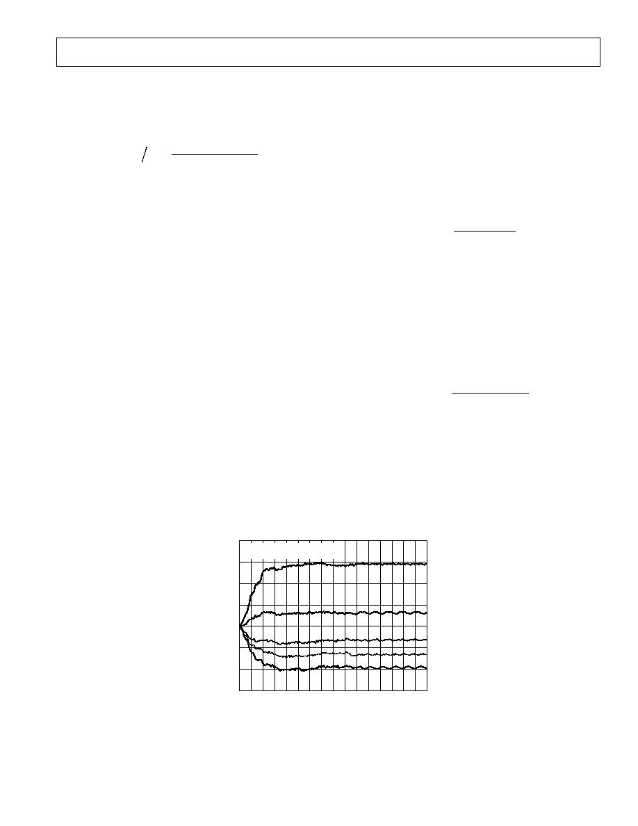
Long Term Stability
Typical shift in output voltage over 1000 hours at a controlled
temperature. Figure 1 shows a sample of parts measured at
different intervals in a controlled environment of 50
°C for
1000 hours.
V
V
t
V
t
V
ppm
V
t
V
t
V
t
O
O
O
O
O
O
O
=
( )
-
( )
[ ]
=
( )
-
( )
( )
×
0
1
0
1
0
6
10
Where:
V
O
(t
0
) = V
O
at at time 0.
V
O
(t
1
) = V
O
after 1000 hours operation at a controlled
temperature.
Thermal Hysteresis (V
O_HYS
)
The change of output voltage after the device is cycled through
temperature from +25 C to 40 C to +85
°C and back to +25 C.
This is a typical value from a sample of parts put through such
a cycle.
V
V
C
V
V
ppm
V
C
V
V
C
O
HYS
O
O TC
O
HYS
O
O TC
O
_
_
_
_
=
( )
-
[ ]
=
°
( )
-
°
( )
×
25
25
25
10
6
o
Where:
V
O
(25 C) = V
O
at 25 C.
V
O_TC
= V
O
at 25 C after temperature cycle at +25 C to
40 C to +85 C and back to +25 C.
150
DRIFT ppm
200
150
TIME Hours
0
100
50
0
50
100
86
176
250
324
440
640
840
1040
DATA TAKEN IN CONTROLLED
ENVIRONMENT @ 50 C 1 C
Figure 1. ADR391 Typical Long-Term Drift over 1000 Hours
REV. A
ADR390/ADR391
6
TEMPERATURE C
2.042
40
15
V
OUT
V
10
35
60
85
2.044
2.046
2.048
2.050
2.052
2.054
SAMPLE 1
SAMPLE 2
SAMPLE 3
TPC 1. ADR390 Output Voltage vs. Temperature
TEMPERATURE C
2.494
40
15
V
OUT
V
10
35
60
85
2.496
2.498
2.500
2.502
2.504
2.506
SAMPLE 1
SAMPLE 2
SAMPLE 3
TPC 2. ADR391 Output Voltage vs. Temperature
INPUT VOLTAGE V
140
120
40
2.5
15.0
5.0
SUPPLY CURRENT
A
7.5
10.0
12.5
100
80
60
+85 C
+25 C
40 C
TPC 3. ADR390 Supply Current vs. Input Voltage
INPUT VOLTAGE V
140
120
40
2.5
15.0
5.0
SUPPLY CURRENT
A
7.5
10.0
12.5
100
80
60
+85 C
+25 C
40 C
TPC 4. ADR391 Supply Current vs. Input Voltage
TEMPERATURE C
10
40
15
LOAD REGULATION
ppm/mA
10
35
60
85
15
20
25
30
35
40
I
L
= 0mA TO 5mA
V
IN
= 5.0V
V
IN
= 3.0V
TPC 5. ADR390 Load Regulation vs. Temperature
TEMPERATURE C
10
40
15
LOAD REGULATION
ppm/mA
10
35
60
85
15
20
25
30
35
40
V
IN
= 5.0V
V
IN
= 3.5V
I
L
= 0mA TO 5mA
TPC 6. ADR391 Load Regulation vs. Temperature
Typical Performance Characteristics
REV. A
ADR390/ADR391
7
TEMPERATURE C
0
40
15
LINE REGULATION
ppm/V
10
35
60
85
5
1
2
3
4
V
IN
= 2.5V TO 15V
TPC 7. ADR390 Line Regulation vs. Temperature
TEMPERATURE C
0
40
15
LINE REGULATION
ppm/V
10
35
60
85
5
1
2
3
4
V
IN
= 2.8V TO 15V
TPC 8. ADR391 Line Regulation vs. Temperature
LOAD CURRENT mA
0.8
0
0
5
1
DIFFERENTIAL VOLTAGE
V
2
3
4
0.6
0.4
0.2
40 C
+85 C
+25 C
TPC 9. ADR390 Minimum Input-Output Voltage
Differential vs. Load Current
LOAD CURRENT mA
0.8
0
0
5
1
DIFFERENTIAL VOLTAGE
V
2
3
4
0.6
0.4
0.2
40 C
+85 C
+25 C
TPC 10. ADR391 Minimum Input-Output Voltage
Differential vs. Load Current
V
OUT
DEVIATION mV
60
50
0
0.24
0.30
0.12
FREQUENCY
0
0.06
0.18
40
30
20
10
0.18
0.06
0.12
0.24
TEMPERATURE: +25 C 40 C +85 C +25 C
TPC 11. ADR390 V
OUT
Hysteresis Distribution
V
OUT
DEVIATION mV
70
50
0
0.56
0.26
FREQUENCY
0.04
0.19
40
30
20
10
0.41
0.11
0.34
60
TEMPERATURE: +25 C 40 C +85 C +25 C
TPC 12. ADR391 V
OUT
Hysteresis Distribution
REV. A
ADR390/ADR391
8
FREQUENCY Hz
1k
100
10
10k
100
VOLTAGE NOISE DENSITY
nV/ Hz
1k
ADR390
ADR391
V
IN
= 5V
TPC 13. Voltage Noise Density vs. Frequency
VOLTAGE
2
V/DIV
TIME 1 Sec/DIV
0
0
0
0
0
0
0
0
0
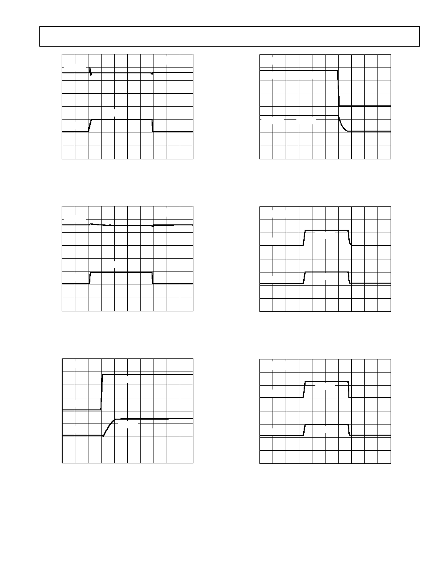
TPC 14. ADR391 Typical Voltage Noise 0.1 Hz to 10 Hz
VOLTAGE
100
V/DIV
TIME 10ms/DIV
0
0
0
0
0
0
0
0
0
TPC 15. ADR391 Voltage Noise 10 Hz to 10 kHz
VOLTAGE
TIME 10 s/DIV
0
0
0
0
0
0
0
0
C
BYPASS
= 0 F
LINE
INTERRUPTION
V
OUT
0.5V/DIV
1V/DIV
TPC 16. ADR391 Line Transient Response
VOLTAGE
TIME 10 s/DIV
0
0
0
0
0
0
0
0
0
C
BYPASS
= 0.1 F
LINE
INTERRUPTION
V
OUT
0.5V/DIV
1V/DIV
TPC 17. ADR391 Line Transient Response
VOLTAGE
1V/DIV
TIME 200 s/DIV
0
0
0
0
0
0
0
0
0
C
L
= 0nF
V
LOAD
ON
V
OUT
LOAD OFF
TPC 18. ADR391 Load Transient Response
REV. A
ADR390/ADR391
9
VOLTAGE
1V/DIV
TIME 200 s/DIV
0
0
0
0
0
0
0
0
0
C
L
= 1nF
V
OUT
V
LOAD
ON
LOAD OFF
TPC 19. ADR391 Load Transient Response
VOLTAGE
1V/DIV
TIME 200 s/DIV
0
0
0
0
0
0
0
0
0
C
L
= 100nF
V
OUT
V
LOAD
ON
LOAD OFF
TPC 20. ADR391 Load Transient Response
VOLTAGE
TIME 20 s/DIV
0
0
0
0
0
0
0
0
0
V
OUT
V
IN
V
IN
= 15V
5V/DIV
2V/DIV
TPC 21. ADR391 Turn-On Response Time at 15 V
VOLTAGE
TIME 40 s/DIV
0
0
0
0
0
0
0
0
0
V
OUT
V
IN
V
IN
= 15V
5V/DIV
2V/DIV
TPC 22. ADR391 Turn-Off Response at 15 V
VOLTAGE
TIME 200 s/DIV
0
0
0
0
0
0
0
0
0
C
BYPASS
= 0.1 F
V
IN
V
OUT
5V/DIV
2V/DIV
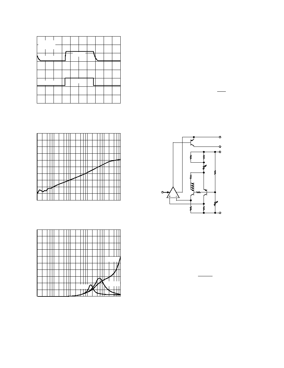
TPC 23. ADR391 Turn-On/Turn-Off Response at 5 V
VOLTAGE
TIME 200 s/DIV
0
0
0
0
0
0
0
0
0
R
L
= 500
V
OUT
V
IN
5V/DIV
2V/DIV
TPC 24. ADR391 Turn-On/Turn-Off Response at 5 V
REV. A
ADR390/ADR391
10
VOLTAGE
5V/DIV
TIME 200 s/DIV
0
0
0
0
0
0
0
0
0
R
L
= 500
C
L
= 100nF
V
OUT
V
IN
5V/DIV
2V/DIV
TPC 25. ADR391 Turn-On/Turn-Off Response at 5 V
FREQUENCY Hz
10
1M
100
RIPPLE REJECTION
dB
1k
10k
100k
80
60
120
40
20
0
20
40
60
80
100
TPC 26. Ripple Rejection vs. Frequency
FREQUENCY Hz
10
1M
100
OUTPUT IMPEDANCE
1k
10k
100k
100
90
0
80
70
60
50
40
30
20
10
C
L
= 0 F
C
L
= 0.1 F
C
L
= 1 F
TPC 27. Output Impedance vs. Frequency
THEORY OF OPERATION
Bandgap references are the high-performance solution for low
supply voltage and low power voltage reference applications,
and the ADR390/ADR391 is no exception. The uniqueness of
this product lies in its architecture. By observing Figure 2, the
ideal zero TC bandgap voltage is referenced to the output, not to
ground. Therefore, if noise exists on the ground line, it will be
greatly attenuated on V
OUT
. The bandgap cell consists of the
pnp pair Q51 and Q52, running at unequal current densities.
The difference in V
BE
results in a voltage with a positive TC
which is amplified up by the ratio of
2
58
54
×
R
R
. This PTAT
voltage, combined with V
BE
s of Q51 and Q52 produce the stable
bandgap voltage.
Reduction in the bandgap curvature is performed by the ratio of
the resistors R44 and R59, one of which is linearly temperature
dependent. Precision laser trimming and other patented circuit
techniques are used to further enhance the drift performance.
SHDN
R60
Q51
R54
R61
R53
Q52
R58
R59
R44
R48
R49
Q1
V
IN
V
OUT
(FORCE)
V
OUT
(SENSE)
GND
Figure 2. Simplified Schematic
Device Power Dissipation Considerations
The ADR390/ADR391 is capable of delivering load currents to
5 mA with an input voltage that ranges from 2.8 V (ADR391 only)
to 15 V. When this device is used in applications with large input
voltages, care should be taken to avoid exceeding the specified maxi-
mum power dissipation or junction temperature that could result in
premature device failure. The following formula should be used to
calculate a device's maximum junction temperature or dissipation:
P
T
T
D
A
=
-
J
JA
In this equation, T
J
and T
A
are, respectively, the junction and
ambient temperatures, P
D
is the device power dissipation, and
JA
is the device package thermal resistance.
Shutdown Mode Operation
The ADR390/ADR391 includes a shutdown feature that is TTL/
CMOS level compatible. A logic LOW or a zero volt condition on
the
SHDN pin is required to turn the device off. During shutdown,
the output of the reference becomes a high impedance state where
its potential would then be determined by external circuitry. If the
shutdown feature is not used, the
SHDN pin should be connected
to V
IN
(Pin 2).
REV. A
ADR390/ADR391
11
APPLICATIONS
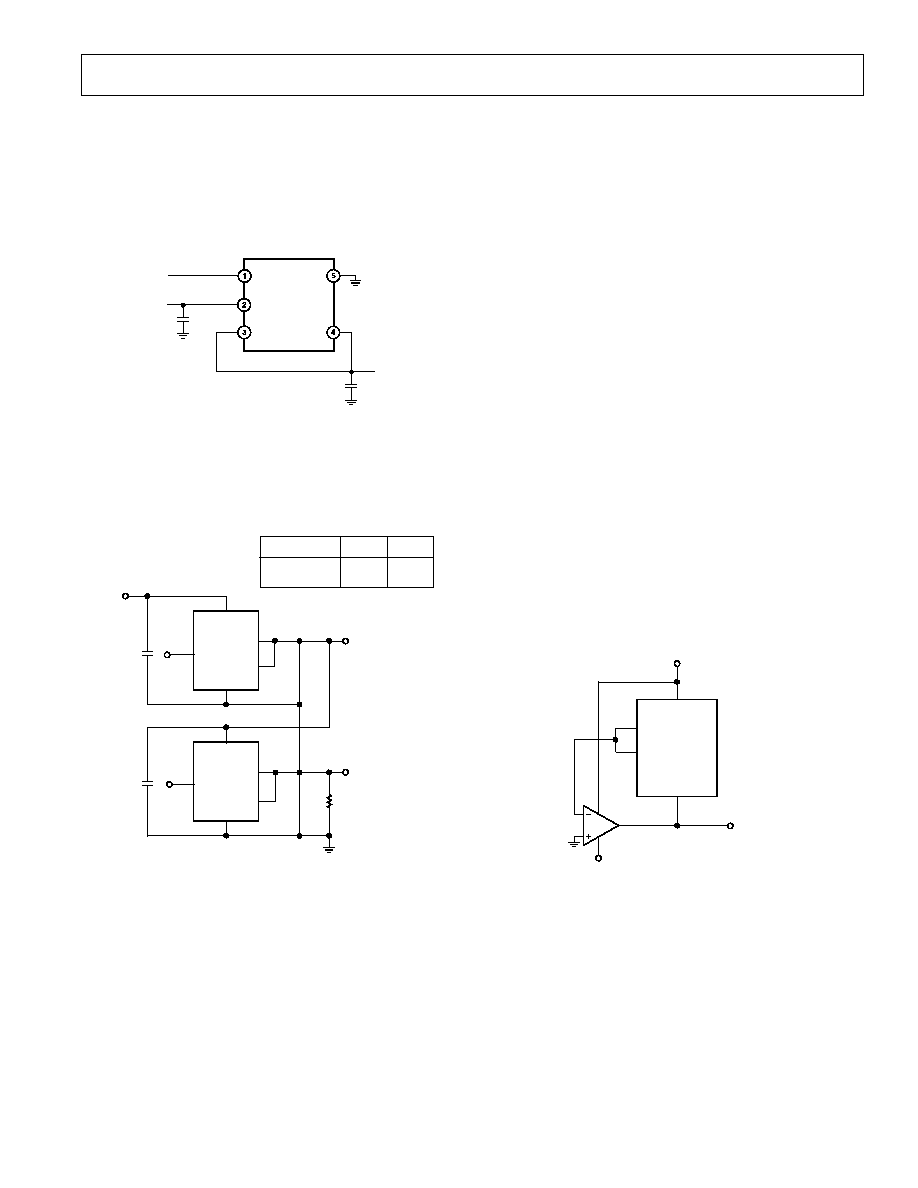
BASIC VOLTAGE REFERENCE CONNECTION
The circuit in Figure 3 illustrates the basic configuration for the
ADR39x family. Decoupling capacitors are not required for cir-
cuit stability. The ADR39x family is capable of driving capacitive
loads from 0
µF to 10 µF. However, a 0.1 µF ceramic output
capacitor is recommended to absorb and deliver the charge as is
required by a dynamic load.
SHUTDOWN
INPUT
C
B
0.1 F
C
B
0.1 F
*
*
OUTPUT
* NOT REQUIRED
ADR39x
SHDN
V
IN
V
OUT(S)
GND
V
OUT(F)
Figure 3.
Stacking Reference ICs for Arbitrary Outputs
Some applications may require two reference voltage sources which
are a combined sum of standard outputs. The following circuit
shows how this "stacked output" reference can be implemented:
OUTPUT TABLE
U1/U2
ADR390/ADR390
ADR391/ADR391
V
OUT1
(V)
2.048
2.5
V
OUT2
(V)
4.096
5.0
SHDN
GND
V
OUT(F)
V
IN
2 U2
1
5
C1
0.1 F
V
IN
4
V
OUT2
SHDN
GND
V
OUT(F)
V
IN
2 U1
1
5
C2
0.1 F
4
V
OUT1
R1
3.9k
3
V
OUT(S)
V
OUT(S)
3
Figure 4. Stacking Voltage References with the ADR390/
ADR391
Two reference ICs are used, fed from an unregulated input,
V
IN
. The outputs of the individual ICs are simply connected in
series which provides two output voltages V
OUT1
and V
OUT2
.
V
OUT1
is the terminal voltage of U1, while V
OUT2
is the sum of this
voltage and the terminal voltage of U2. U1 and U2 are simply
chosen for the two voltages that supply the required outputs (see
Output Table). For example, if both U1 and U2 are ADR391s,
V
OUT1
is 2.5 V and V
OUT2
is 5.0 V.
While this concept is simple, a precaution is in order. Since the
lower reference circuit must sink a small bias current from U2,
plus the base current from the series PNP output transistor in
U2, either the external load of U1 or R1 must provide a path for
this current. If the U1 minimum load is not well defined, the
resistor R1 should be used, set to a value that will conservatively
pass 600
µA of current with the applicable V
OUT1
across it. Note
that the two U1 and U2 reference circuits are locally treated as
macrocells, each having its own bypasses at input and output for best
stability. Both U1 and U2 in this circuit can source dc currents up to
their full rating. The minimum input voltage, V
IN,
is determined by
the sum of the outputs, V
OUT2
, plus the dropout voltage of U2.
A Negative Precision Reference without Precision Resistors
In many current-output CMOS DAC applications where the
output signal voltage must be of the same polarity as the reference
voltage, it is often required to reconfigure a current-switching
DAC into a voltage-switching DAC through the use of a 1.25 V
reference, an op amp, and a pair of resistors. Using a current-
switching DAC directly requires the need for an additional
operational amplifier at the output to reinvert the signal. A negative
voltage reference is then desirable from the point that an additional
operational amplifier is not required for either reinversion (current-
switching mode) or amplification (voltage switching mode) of the
DAC output voltage. In general, any positive voltage reference can
be converted into a negative voltage reference through the use of an
operational amplifier and a pair of matched resistors in an inverting
configuration. The disadvantage to this approach is that the largest
single source of error in the circuit is the relative matching of the
resistors used.
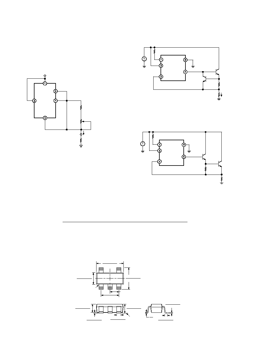
A Negative Precision Reference without Precision Resistors
A negative reference can be easily generated by adding an op
amp, A1 and configured as Figure 5 below. V
OUTF
and V
OUTS
are at virtual ground and therefore the negative reference can be
taken directly from the output of the op amp. The op amp must
be dual supply, low offset, and rail-to-rail if the negative supply
voltage is close to the reference output.
V
DD
V
DD
V
REF
V
OUT(S)
V
OUT(F)
V
IN
SHDN
GND
ADR39x
A1 = OP777, OP193
A1
2
4
3
5
Figure 5.
Precision Current Source
Many times in low-power applications, the need arises for a preci-
sion current source that can operate on low supply voltages. As
shown in the following figure, the ADR390/ADR391 can be config-
ured as a precision current source. The circuit configuration
illustrated is a floating current source with a grounded load.
The reference's output voltage is bootstrapped across R
SET
,
which sets the output current into the load. With this configura-
tion, circuit precision is maintained for load currents in the range
from the reference's supply current, typically 90
µA to approxi-
mately 5 mA.
REV. A
12
C004192.54/01(A)
PRINTED IN U.S.A.
ADR390/ADR391
OUTLINE DIMENSIONS
Dimensions shown in inches and (mm).
5-Lead SOT-23
(RT Suffix)
0.1181 (3.00)
0.1102 (2.80)
PIN 1
0.0669 (1.70)
0.0590 (1.50)
0.1181 (3.00)
0.1024 (2.60)
1
3
4
5
0.0748 (1.90)
BSC
0.0374 (0.95) BSC
2
0.0079 (0.20)
0.0031 (0.08)
0.0217 (0.55)
0.0138 (0.35)
10
0
0.0197 (0.50)
0.0138 (0.35)
0.0059 (0.15)
0.0019 (0.05)
0.0512 (1.30)
0.0354 (0.90)
SEATING
PLANE
0.0571 (1.45)
0.0374 (0.95)
The ADR390/ADR391 includes a shutdown feature that is
TTL/CMOS level compatible. A logic LOW or a zero volt
condition on the
SHDN pin is required to turn the device off.
During shutdown, the output of the reference becomes a high-
impedance state where its potential would then be determined
by the external circuitry. If the shutdown feature is not used, the
SHDN pin should be connected to V
IN
(Pin 2).
V
IN
ADR39x
GND
V
OUT
I
OUT
R
1
I
SY
ADJUST
R
SET
P
1
R
L
}
SHDN
V
OUT
V
IN
R
1
Figure 6. A Precision Current Source
High-Power Performance with Current Limit
In some cases, the user may want higher output current delivered
to a load and still achieve better than 0.5% accuracy out of the
ADR390/ADR391. The accuracy for a reference is normally
specified on the data sheet with no load. However, the output
voltage changes with load current.
The circuit below provides high current without compromising
the accuracy of the ADR390/ADR391. The series pass transis-
tor Q1 provides up to 1 A load current. The ADR390/ADR391
delivers only the base drive to Q1 through the force pin. The
sense pin of the ADR390/ADR391 is a regulated output and is
connected to the load.
The transistor Q2 protects Q1 during short circuit limit faults by
robbing its base drive. The maximum current is I
LMAX
0.6 V/R
S
.
I
L
V
IN
R1
4.7k
Q2
Q2N2222
Q2N4921
Q1
R
S
R
L
SHDN
V
IN
V
OUT (SENSE)
V
OUT (FORCE)
GND
U1
ADR390/ADR391
Figure 7. ADR390/ADR391 for High-Power Performance
with Current Limit
A similar circuit function can also be achieved with the Darlington
transistor configuration, see Figure 8.
ADR390/ADR391
V
IN
R1
4.7k
Q2
Q2N2222
Q2N4921
R
S
R
L
SHDN
V
IN
V
OUT (SENSE)
V
OUT (FORCE)
GND
Q1
U1
Figure 8. ADR390/ADR391 High Output Current with
Darlington Drive Configuration