Äîêóìåíòàöèÿ è îïèñàíèÿ www.docs.chipfind.ru
a
Preliminary Technical Data
Mixed Signal DSP Controller With CAN
This information applies to a product under development. Its characteristics and specifi-
cations are subject to change without notice. Analog Devices assumes no obligation
regarding future manufacturing unless otherwise agreed to in writing.
One Technology Way, P.O.Box 9106, Norwood, MA 02062-9106, U.S.A.
Tel:781/329-4700 www.analog.com
Fax:781/326-8703
©Analog Devices,Inc., 2002
REV. PrA
PRELIMINARY TECHNICAL DATA
ADSP-21992
MIXED SIGNAL DSP CONTROLLER FEATURES
ADSP-219x, 16-bit, Fixed Point DSP Core with up to 160
MIPS sustained performance
48K Words of On chip RAM, Configured as 32K Words
On chip 24-bit Program RAM and 16K Words On chip
16-bit Data RAM
External Memory Interface
Dedicated Memory DMA Controller for Data/Instruction
Transfer between Internal/External Memory
Programmable PLL and Flexible Clock Generation
Circuitry Enables Full speed Operation from Low
speed Input Clocks
IEEE JTAG Standard 1149.1 Test Access Port Supports
On chip Emulation and System Debugging
8-Channel, 20 MSPS, 14-bit Analog to Digital Converter
System
Three Phase 16-bit Center Based PWM Generation Unit
with 12.5 ns resolution
Dedicated 32-bit Encoder Interface Unit with
Companion Encoder Event Timer
Dual 16-bit Auxiliary PWM Outputs
16 General Purpose Flag I/O Pins
Three Programmable 32-bit Interval Timers
SPI Communications Port with Master or Slave
Operation
Synchronous Serial Communications Port (SPORT)
Capable of Software UART Emulation
Controller Area Network (CAN) Module Fully Compliant
with V2.0B Standard
FUNCTIONAL BLOCK DIAGRAM
ADC
CONTROL
VREF
PIPELINE
FLASH ADC
CLOCK
GENERATOR / PLL
PM ADDRESS/DATA
DM ADDRESS/DATA
I/O
BUS
16K X 16
DMRAM
(BLOCK 1)
32K X 24
PM RAM
(BLOCK 0)
EXTERNAL
MEMORY
INTERFACE
(EMI)
TIMER 0
TIMER 1
TIMER 2
4K X 24
PMROM
(BLOCK 2)
160 MHZ
ADSP-219X
DSP
JTAG
TEST &
EMULATION
ADDRESS
DATA
CONTROL
I/O REGISTERS
PWM
GENERATION
UNIT
ENCODER
INTERFACE
UNIT
(AND EET)
AUXILIARY
PWM
UNIT
FLAG
I/O
SPI
SPORT
WATCHDOG
TIMER
INTERRUPT
CONTROLLER
(ICNTL)
POR
MEMORY DMA
CONTROLLER
CONTROLLER
AREA
NETWORK
(CAN)

For current information contact Analog Devices at (781) 937-1799
ADSP-21992
August 2002
This information applies to a product under development. Its characteristics and specifications are subject to change without notice. Analog
Devices assumes no obligation regarding future manufacturing unless otherwise agreed to in writing.
2
REV. PrA
PRELIMINARY TECHNICAL DATA
Integrated Watchdog Timer
Dedicated Peripheral Interrupt Controller with Software
Priority Control
Multiple Boot Modes
Precision 1.0V Voltage Reference
Integrated Power-On-Reset (POR) Generator
Flexible Power Management with Selectable Powerdown
and Idle Modes
2.5V Internal Operation with 3.3V I/O
Operating Temperature Range of 40ºC to +115ºC
176 pin LQFP package
TARGET APPLICATIONS
Industrial Motor Drives
Un-Interruptible Power Supplies
Optical Networking Control
Data Acquisition Systems
Test and Measurement Systems
Portable Instrumentation
GENERAL NOTE
This data sheet provides preliminary information for the
ADSP-21992 Mixed Signal Digital Signal Processor.
GENERAL DESCRIPTION
The ADSP-21992 is a mixed signal DSP controller based
on the ADSP-219x DSP Core, suitable for a variety of high
performance Industrial Motor Control and Signal Process-
ing applications that require the combination of a high
performance DSP and the mixed signal integration of
embedded control peripherals such as analog to digital con-
version with communications interfaces such as CAN.
The ADSP-21992 integrates the 160 MIPS, fixed point
ADSP-219x family base architecture with a serial port, an
SPI compatible port, a DMA controller, three programma-
ble timers, general purpose Programmable Flag pins,
extensive interrupt capabilities, on chip program and data
memory spaces, and a complete set of embedded control
peripherals that permits fast motor control and signal pro-
cessing in a highly integrated environment.
The ADSP-21992 architecture is code compatible with
previous ADSP-217x based ADMCxxx products. Although
the architectures are compatible, the ADSP-21992, with
ADSP-219x architecture, has a number of enhancements
over earlier architectures. The enhancements to computa-
tional units, data address generators, and program
sequencer make the ADSP-21992 more flexible and easier
to program than the previous ADSP-21xx embedded DSPs.
Indirect addressing options provide addressing flexibility--
premodify with no update, pre- and post-modify by an
immediate 8-bit, two's complement value and base address
registers for easier implementation of circular buffering.
The ADSP-21992 integrates 48K words of on chip memory
configured as 32K words (24-bit) of program RAM, and
16K words (16-bit) of data RAM.
Fabricated in a high speed, low power, CMOS process, the
ADSP-21992 operates with a 6.25 ns instruction cycle time
(160 MIPS). All instructions, except two multiword
instructions, execute in a single DSP cycle.
The ADSP-21992's flexible architecture and comprehen-
sive instruction set support multiple operations in parallel.
For example, in one processor cycle, the ADSP-21992 can:
·
Generate an address for the next instruction fetch
·
Fetch the next instruction
·
Perform one or two data moves
·
Update one or two data address pointers
·
Perform a computational operation
These operations take place while the processor
continues to:
·
Receive and transmit data through the serial port
·
Receive or transmit data over the SPI port
·
Access external memory through the external memory
interface
·
Decrement the timers
·
Operate the embedded control peripherals (ADC, PWM,
EIU, etc.)
DSP Core Architecture
·
6.25 ns instruction cycle time (internal), for up to 160
MIPS sustained performance
·
ADSP-218x family code compatible with the same easy
to use algebraic syntax
·
Single cycle instruction execution
·
Up to 1 Mwords of addressable memory space with
twenty four bits of addressing width
·
Dual purpose program memory for both instruction and
data storage
·
Fully transparent Instruction Cache allows dual operand
fetches in every instruction cycle
·
Unified memory space permits flexible address genera-
tion, using two independent DAG units
·
Independent ALU, Multiplier/Accumulator, and barrel
Shifter computational units with dual 40-bit
accumulators
·
Single cycle context switch between two sets of computa-
tional and DAG registers
·
Parallel execution of computation and memory
instructions
·
Pipelined architecture supports efficient code execution
at speeds up to 160 MIPS
·
Register file computations with all non-conditional,
non-parallel computational instructions
·
Powerful Program Sequencer provides zero overhead
looping and conditional instruction execution
This information applies to a product under development. Its characteristics and specifications are subject to change without notice. Analog
Devices assumes no obligation regarding future manufacturing unless otherwise agreed to in writing.
3
REV. PrA
For current information contact Analog Devices at (781) 937-1799
ADSP-21992
August 2002
PRELIMINARY TECHNICAL DATA
·
Architectural enhancements for compiled C code
efficiency
·
Architecture enhancements beyond ADSP-218x family
are supported with instruction set extensions for added
registers, ports, and peripherals.
The clock generator module of the ADSP-21992 includes
Clock Control logic that allows the user to select and change
the main clock frequency. The module generates two output
clocks; the DSP core clock, CCLK, and the peripheral
clock, HCLK. CCLK can sustain clock values of up to 160
MHz, while HCLK can be equal to CCLK or CCLK/2 for
values up to a maximum 80MHz peripheral clock.
The ADSP-21992 instruction set provides flexible data
moves and multifunction (one or two data moves with a
computation) instructions. Every single word instruction
can be executed in a single processor cycle. The
ADSP-21992 assembly language uses an algebraic syntax
for ease of coding and readability. A comprehensive set of
development tools supports program development.
The block diagram
Figure 1
shows the architecture of the
embedded ADSP-219x core. It contains three independent
computational units: the ALU, the multiplier/accumulator
(MAC), and the shifter. The computational units process
16-bit data from the register file and have provisions to
support multiprecision computations. The ALU performs
a standard set of arithmetic and logic operations; division
primitives are also supported. The MAC performs single
cycle multiply, multiply/add, and multiply/subtract opera-
tions. The MAC has two 40-bit accumulators, which help
with overflow. The shifter performs logical and arithmetic
shifts, normalization, denormalization, and derive exponent
operations. The shifter can be used to efficiently implement
numeric format control, including multiword and block
floating point representations.
Register usage rules influence placement of input and
results within the computational units. For most operations,
the computational units' data registers act as a data register
file, permitting any input or result register to provide input
to any unit for a computation. For feedback operations, the
computational units let the output (result) of any unit be
Figure 1. ADSP-21992 DSP Block Diagram
I/O REGISTERS
(MEMORY MAPPED)
CONTROL
STATUS
BUFFERS
I/O PROCESSOR
INTERRUPT CONTROLLER/
TIMERS/FLAGS
CACHE
64 X 24-BIT
JTAG
TEST &
EMULATION
ADDR BUS
MUX
EXTERNAL MEMORY
INTERFACE
EXTERNAL PORT
DATA BUS
MUX
PM ADDRESS BUS
DM ADDRESS BUS
PM DATA BUS
DM DATA BUS
BUS
CONNECT
(PX)
ADSP-219X
DSP CORE
PROGRAM
SEQUENCER
DATA
REGISTER
FILE
MULT
BARREL
SHIFTER
ALU
DMA
CONTROLLER
INPUT
REGISTERS
RESULT
REGISTERS
16 X 16-BIT
AHB CORE
INTERFACE
DAG1
4 X 4 X 16
DAG2
4 X 4 X 16
DATA
DATA
ADDRESS
TWO INDEPENDENT BLOCKS
INTERNAL SRAM
ADDRESS
DMA
DATA
DMA
ADDRESS
EMBEDDED
CONTROL
PERIPHERALS AND
COMMUNICATIONS
PORTS
For current information contact Analog Devices at (781) 937-1799
ADSP-21992
August 2002
This information applies to a product under development. Its characteristics and specifications are subject to change without notice. Analog
Devices assumes no obligation regarding future manufacturing unless otherwise agreed to in writing.
4
REV. PrA
PRELIMINARY TECHNICAL DATA
input to any unit on the next cycle. For conditional or mul-
tifunction instructions, there are restrictions on which data
registers may provide inputs or receive results from each
computational unit. For more information, see the
ADSP-219x DSP Instruction Set Reference.
A powerful program sequencer controls the flow of instruc-
tion execution. The sequencer supports conditional jumps,
subroutine calls, and low interrupt overhead. With internal
loop counters and loop stacks, the ADSP-21992 executes
looped code with zero overhead; no explicit jump instruc-
tions are required to maintain loops.
Two data address generators (DAGs) provide addresses for
simultaneous dual operand fetches (from data memory and
program memory). Each DAG maintains and updates four
16-bit address pointers. Whenever the pointer is used to
access data (indirect addressing), it is pre- or post-modified
by the value of one of four possible modify registers. A length
value and base address may be associated with each pointer
to implement automatic modulo addressing for circular
buffers. Page registers in the DAGs allow circular addressing
within 64K word boundaries of each of the 256 memory
pages, but these buffers may not cross page boundaries.
Secondary registers duplicate all the primary registers in the
DAGs; switching between primary and secondary registers
provides a fast context switch.
Efficient data transfer in the core is achieved with the use of
internal buses:
·
Program Memory Address (PMA) Bus
·
Program Memory Data (PMD) Bus
·
Data Memory Address (DMA) Bus
·
Data Memory Data (DMD) Bus
·
Direct Memory Access Address Bus
·
Direct Memory Access Data Bus
The two address buses (PMA and DMA) share a single
external address bus, allowing memory to be expanded off
chip, and the two data buses (PMD and DMD) share a
single external data bus. Boot memory space and I/O
memory space also share the external buses.
Program memory can store both instructions and data, per-
mitting the ADSP-21992 to fetch two operands in a single
cycle, one from program memory and one from data
memory. The DSP's dual memory buses also let the
embedded ADSP-219x core fetch an operand from data
memory and the next instruction from program memory in
a single cycle.
Memory Architecture
The ADSP-21992 provides 48K words of on chip SRAM
memory. This memory is divided into two blocks; a 32K x
24-bit (block 0) and a 16K x 16-bit (block 1). In addition,
the ADSP-21992 provides a 4k x 24-bit block of program
memory boot ROM (that is reserved by ADI for boot load
routines). The memory map of the ADSP-21992 is illus-
trated in Figure 2.
As shown in Figure 2, the two internal memory RAM blocks
reside in memory page 0. The entire DSP memory map
consists of 256 pages (pages 0 to 255), and each page is 64
kWords long. External memory space consists of four
memory banks (banks 0-3) and supports a wide variety of
memory devices. Each bank is selectable using unique
memory select lines (MS3 - MS0) and has configurable page
boundaries, wait states, and wait state modes. The 4K words
of on chip boot ROM populates the top of page 255, while
the remaining 254 pages are addressable off chip. I/O
memory pages differ from external memory in that they are
1K word long, and the external I/O pages have their own
select pin (IOMS). Pages 0-31 of I/O memory space reside
on chip and contain the configuration registers for the
peripherals. Both the ADSP_219x core and DMA capable
peripherals can access the DSP's entire memory map.
NOTE: The physical external memory addresses are limited
by 20 address lines, and are determined by the external data
width and packing of the external memory space. The
Strobe signals (MS3 - 0) can be programmed to allow the
user to change starting page addresses at run time.
Internal (On chip) Memory
The ADSP-21992's unified program and data memory
space consists of 16M locations that are accessible through
two 24-bit address buses, the PMA and DMA buses. The
Figure 2. ADSP-21992 DSP Core Memory Map at Reset
0x000000
0x00 7FFF
0x00 BFFF
0x01 0000
0x40 0000
0x80 0000
0xC0 0000
0xFF 0000
0xFF 1000
0xFF FFFF
0x00 8000
0x00 C000
0x00 FFFF
0xFF 0FFF
PAGE 0 (64K) ON-CHIP
(0 WAIT STATE)
EXTERNAL MEMORY
(4M - 64K)
PAGES 1 TO 63
BANK 0
(OFF-CHIP)
MS0
PAGE 255
(ON-CHIP
EXTERNAL MEMORY
EXTERNAL MEMORY
PAGES 64 TO 127
BANK 1
(OFF-CHIP)
PAGES 128 TO 191
BANK 2
(OFF-CHIP)
PAGES 192 TO 254
BANK 0
(OFF-CHIP)
MS1
MS2
MS3
EXTERNAL MEMORY
(4M - 64K)
BLOCK 0: 32K X 24-BIT RAM
RESERVED (16K)
BLOCK 1: 16K X 16-BIT RAM
BLOCK 2: 4K X 24-BIT
PM ROM
UNUSED ON-CHIP
MEMORY (60K)
This information applies to a product under development. Its characteristics and specifications are subject to change without notice. Analog
Devices assumes no obligation regarding future manufacturing unless otherwise agreed to in writing.
5
REV. PrA
For current information contact Analog Devices at (781) 937-1799
ADSP-21992
August 2002
PRELIMINARY TECHNICAL DATA
DSP uses slightly different mechanisms to generate a 24-bit
address for each bus. The DSP has three functions that
support access to the full memory map.
·
The DAGs generate 24-bit addresses for data fetches from
the entire DSP memory address range. Because DAG
index (address) registers are 16 bits wide and hold the
lower 16 bits of the address, each of the DAGs has its own
8-bit page register (DMPGx) to hold the most significant
eight address bits. Before a DAG generates an address,
the program must set the DAG's DMPGx register to the
appropriate memory page. The DMPG1 register is also
used as a page register when accessing external memory.
The program must set DMPG1 accordingly, when
accessing data variables in external memory. A 'C'
program macro is provided for setting this register.
·
The Program Sequencer generates the addresses for
instruction fetches. For relative addressing instructions,
the program sequencer bases addresses for relative jumps,
calls, and loops on the 24-bit Program Counter (PC). In
direct addressing instructions (two word instructions),
the instruction provides an immediate 24-bit address
value. The PC allows linear addressing of the full 24-bit
address range.
·
For indirect jumps and calls that use a 16-bit DAG
address register for part of the branch address, the
Program Sequencer relies on an 8-bit Indirect Jump page
(IJPG) register to supply the most significant eight
address bits. Before a cross page jump or call, the program
must set the program sequencer's IJPG register to the
appropriate memory page.
The ADSP-21992 has 4K word of on chip ROM that holds
boot routines. The DSP starts executing instructions from
the on chip boot ROM, which starts the boot process.
For
more information, see Booting Modes on page 14.
The on
chip boot ROM is located on Page 255 in the DSP's
memory space map, starting at address 0xFF0000.
External (Off Chip) Memory
Each of the ADSP-21992's off chip memory spaces has a
separate control register, so applications can configure
unique access parameters for each space. The access param-
eters include read and write wait counts, wait state
completion mode, I/O clock divide ratio, write hold time
extension, strobe polarity, and data bus width. The core
clock and peripheral clock ratios influence the external
memory access strobe widths.
For more information, see
Clock Signals on page 13.
The off chip memory spaces are:
·
External memory space (MS30 pins)
·
I/O memory space (IOMS pin)
·
Boot memory space (BMS pin)
All of these off chip memory spaces are accessible through
the External Port, which can be configured for 8-bit or
16-bit data widths.
External Memory Space
External memory space consists of four memory banks.
These banks can contain a configurable number of 64 k
Word pages. At reset, the page boundaries for external
memory have Bank0 containing pages 1 to 63, Bank1 con-
taining pages 64 to 127, Bank2 containing pages 128 to 191,
and Bank3 containing pages 192 to 254. The MS3-MS0
memory bank pins select Banks 3-0, respectively. Both the
ADSP-219x core and DMA capable peripherals can access
the DSP's external memory space.
All accesses to external memory are managed by the
External Memory Interface Unit (EMI).
I/O Memory Space
The ADSP-21992 supports an additional external memory
called I/O memory space. The IO space consists of 256
pages, each containing 1024 addresses. This space is
designed to support simple connections to peripherals (such
as data converters and external registers) or to bus interface
ASIC data registers. The first 32K addresses (IO pages 0 to
31) are reserved for on chip peripherals. The upper 224k
addresses (IO pages 32 to 255) are available for external
peripheral devices. External I/O pages have their own select
pin (IOMS). The DSP instruction set provides instructions
for accessing I/O space.
Boot Memory Space
Boot memory space consists of one off chip bank with 254
pages. The BMS memory bank pin selects boot memory
space. Both the ADSP-219x core and DMA capable periph-
Figure 3. ADSP-21992 I/O Memory Map
ON-CHIP
PERIPHERALS
16-BITS
OFF-CHIP
PERIPHERALS
16-BITS
PAGES 0 TO 31
1024 WORDS/PAGE
2 PERIPHERALS/PAGE
0X00::0X000
0X20::0X000
0XFF::0X3FF
0X1F::0X3FF
PAGES 32 TO 255
1024 WORDS/PAGE

For current information contact Analog Devices at (781) 937-1799
ADSP-21992
August 2002
This information applies to a product under development. Its characteristics and specifications are subject to change without notice. Analog
Devices assumes no obligation regarding future manufacturing unless otherwise agreed to in writing.
6
REV. PrA
PRELIMINARY TECHNICAL DATA
erals can access the DSP's off chip boot memory space. After
reset, the DSP always starts executing instructions from the
on chip boot ROM.
Bus Request and Bus Grant
The ADSP-21992 can relinquish control of the data and
address buses to an external device. When the external
device requires access to the bus, it asserts the bus request
(BR) signal. The (BR) signal is arbitrated with core and
peripheral requests. External Bus requests have the lowest
priority. If no other internal request is pending, the external
bus request will be granted. Due to synchronizer and arbi-
tration delays, bus grants will be provided with a minimum
of three peripheral clock delays. The ADSP-21992 will
respond to the bus grant by:
·
Three stating the data and address buses and the MS30,
BMS, IOMS, RD, and WR output drivers.
·
Asserting the bus grant (BG) signal.
The ADSP-21992 will halt program execution if the bus is
granted to an external device and an instruction fetch or
data read/write request is made to external general purpose
or peripheral memory spaces. If an instruction requires two
external memory read accesses, the bus will not be granted
between the two accesses. If an instruction requires an
external memory read and an external memory write access,
the bus may be granted between the two accesses. The
external memory interface can be configured so that the
core will have exclusive use of the interface. DMA and Bus
Requests will be granted. When the external device releases
BR, the DSP releases BG and continues program execution
from the point at which it stopped.
The bus request feature operates at all times, even while the
DSP is booting and RESET is active.
The ADSP-21992 asserts the BGH pin when it is ready to
start another external port access, but is held off because
the bus was previously granted. This mechanism can be
extended to define more complex arbitration protocols for
implementing more elaborate multimaster systems.
DMA Controller
The ADSP-21992 has a DMA controller that supports
automated data transfers with minimal overhead for the
DSP core. Cycle stealing DMA transfers can occur between
the ADSP-21992's internal memory and any of its DMA
capable peripherals. Additionally, DMA transfers can be
accomplished between any of the DMA capable peripherals
and external devices connected to the external memory
interface. DMA capable peripherals include the SPORT
and SPI ports, and ADC Control module. Each individual
DMA capable peripheral has a dedicated DMA channel. To
describe each DMA sequence, the DMA controller uses a
set of parameters--called a DMA descriptor. When succes-
sive DMA sequences are needed, these DMA descriptors
can be linked or chained together, so the completion of one
DMA sequence auto initiates and starts the next sequence.
DMA sequences do not contend for bus access with the DSP
core, instead DMAs "steal" cycles to access memory.
All DMA transfers use the DMA bus shown in
Figure 1 on
page 3
. Because all of the peripherals use the same bus,
arbitration for DMA bus access is needed. The arbitration
for DMA bus access appears in
Table 1
.
DSP Peripherals Architecture
The ADSP-21992 contains a number of special purpose,
embedded control peripherals, which can be seen in the
Functional Block diagram on page 1. The ADSP-21992
contains a high performance, 8-channel, 14-bit ADC
system with dual channel simultaneous sampling ability
across 4 pairs of inputs. An internal precision voltage
reference is also available as part of the ADC system. In
addition, a three phase, 16-bit, center based PWM genera-
tion unit can be used to produce high accuracy PWM signals
with minimal processor overhead. The ADSP-21992 also
contains a flexible incremental encoder interface unit for
position sensor feedback; two adjustable frequency auxiliary
PWM outputs, 16 lines of digital I/O; a 16-bit watchdog
timer; three general purpose timers and an interrupt con-
troller that manages all peripheral interrupts. Finally, the
ADSP-21992 contains an integrated power-on-reset (POR)
circuit that can be used to generate the required reset signal
for the device on power-on.
The ADSP-21992 has an external memory interface that is
shared by the DSP's core, the DMA controller, and DMA
capable peripherals, which include the ADC, SPORT, and
SPI communication ports. The external port consists of a
16-bit data bus, a 20-bit address bus, and control signals.
Figure 4. ADSP-21992 Boot Memory Map
PAGES 1 TO 254
64K WORDS/PAGE
0x01 0000
0xFE 0000
OFF-CHIP
BOOT MEMORY
16-BITS
Table 1. I/O Bus Arbitration Priority
DMA Bus Master
Arbitration Priority
SPORT Receive DMA
0--Highest
SPORT Transmit DMA
1
ADC Control DMA
2
SPI0 Receive/Transmit DMA
3
Memory DMA
4--Lowest

This information applies to a product under development. Its characteristics and specifications are subject to change without notice. Analog
Devices assumes no obligation regarding future manufacturing unless otherwise agreed to in writing.
7
REV. PrA
For current information contact Analog Devices at (781) 937-1799
ADSP-21992
August 2002
PRELIMINARY TECHNICAL DATA
The data bus is configurable to provide an 8 or 16 bit
interface to external memory. Support for word packing lets
the DSP access 16- or 24-bit words from external memory
regardless of the external data bus width.
The memory DMA controller lets the ADSP-21992 move
data and instructions from between memory spaces: inter-
nal-to-external, internal-to-internal, and external-to-
external. On chip peripherals can also use this controller for
DMA transfers.
The embedded ADSP-219x core can respond to up to
seventeen interrupts at any given time: three internal (stack,
emulator kernel, and power down), two external (emulator
and reset), and twelve user defined (peripherals) interrupts.
Programmers assign each of the 32 peripheral interrupt
requests to one of the 12 user defined interrupts. These
assignments determine the priority of each peripheral for
interrupt service.
The following sections provide a functional overview of the
ADSP-21992 peripherals.
Serial Peripheral Interface (SPI) Port
The Serial Peripheral Interface (SPI) Port provides func-
tionality for a generic configurable serial port interface
based on the SPI standard, which enables the DSP to com-
municate with multiple SPI compatible devices. Key
features of the SPI port are:
·
Interface to host microcontroller or serial EEPROM
·
Master or slave operation (3 Wire Interface MISO,
MOSI, SCK)
·
Data rates to 20 Mbaud (16-bit baud rate selector)
·
8 or 16-bit transfer
·
Programmable clock phase & polarity
·
Broadcast Mode - 1 master, multiple slaves
·
DMA capability & Dedicated interrupts
·
PF0 can be used as Slave Select Input Line
·
PF1-PF7 can be used as external Slave Select output
SPI is a 3 wire interface consisting of 2 data pins (MOSI
and MISO), one clock pin (SCK), and a single Slave Select
input (SPISS0) that is multiplexed with the PF0 Flag IO
line and seven Slave Select outputs (SPISEL1 to SPISEL7)
that are multiplexed with the PF1 to PF7 Flag IO lines. The
SPISS0 input is used to select the ADSP-21992 as a slave
to an external master. The SPISEL1 to SPISEL7 outputs
can be used by the ADSP-21992 (acting as a master) to
select/enable up to seven external slaves in an multi device
SPI configuration. In a multimaster or a multi device con-
figuration, all MOSI pins are tied together, all MISO pins
are tied together, and all SCK pins are tied together.
During transfers, the SPI port simultaneously transmits and
receives by serially shifting data in and out on the serial data
line. The serial clock line synchronizes the shifting and
sampling of data on the serial data line.
In master mode, the DSP's core performs the following
sequence to set up and initiate SPI transfers:
1.
Enables and configures the SPI port operation (data
size, and transfer format).
2.
Selects the target SPI slave with the SPISELx output
pin (reconfigured Programmable Flag pin).
3.
Defines one or more DMA descriptors in Page 0 of I/O
memory space (optional in DMA mode only).
4.
Enables the SPI DMA engine and specifies transfer
direction (optional in DMA mode only).
5.
In non DMA mode only, reads or writes the SPI port
receive or transmit data buffer.
The SCK line generates the programmed clock pulses for
simultaneously shifting data out on MOSI and shifting
data in on MISO. In DMA mode only, transfers continue
until the SPI DMA word count transitions from 1 to 0.
In slave mode, the DSP core performs the following
sequence to set up the SPI port to receive data from a master
transmitter:
1.
Enables and configures the SPI slave port to match the
operation parameters set up on the master (data size
and transfer format) SPI transmitter.
2.
Defines and generates a receive DMA descriptor in
Page 0 of memory space to interrupt at the end of the
data transfer (optional in DMA mode only).
3.
Enables the SPI DMA engine for a receive access
(optional in DMA mode only).
4.
Starts receiving the data on the appropriate SCK edges
after receiving an SPI chip select on the SPISS0 input
pin (reconfigured Programmable Flag pin)
from a master
In DMA mode only, reception continues until the SPI
DMA word count transitions from 1 to 0. The DSP core
could continue, by queuing up the next DMA descriptor.
A slave mode transmit operation is similar, except the DSP
core specifies the data buffer in memory space from which
to transmit data, generates and relinquishes control of the
transmit DMA descriptor, and begins filling the SPI port
data buffer. If the SPI controller is not ready on time to
transmit, it can transmit a "zero" word.
DSP Serial Port (SPORT)
The ADSP-21992 incorporates a complete synchronous
serial port (SPORT) for serial and multiprocessor commu-
nications. The SPORT supports the following features:
·
Bidirectional: the SPORT has independent transmit and
receive sections.
·
Double buffered: the SPORT section (both receive and
transmit) has a data register for transferring data words
to and from other parts of the processor and a register for
shifting data in or out. The double buffering provides
additional time to service the SPORT.

For current information contact Analog Devices at (781) 937-1799
ADSP-21992
August 2002
This information applies to a product under development. Its characteristics and specifications are subject to change without notice. Analog
Devices assumes no obligation regarding future manufacturing unless otherwise agreed to in writing.
8
REV. PrA
PRELIMINARY TECHNICAL DATA
·
Clocking: the SPORT can use an external serial clock or
generate its own in a wide range of frequencies down to 0
Hz. Maximum clock value is 40 MHz for internally
generated clock.
·
Word length: each SPORT section supports serial data
word lengths from three to sixteen bits that can be trans-
ferred either MSB first or LSB first.
·
Framing: each SPORT section (receive and transmit) can
operate with or without frame synchronization signals for
each data word; with internally generated or externally
generated frame signals; with active high or active low
frame signals; with either of two pulse widths and frame
signal timing.
·
Companding in hardware: each SPORT section can
perform A law and µ law companding according to
CCITT recommendation G.711.
·
Direct Memory Access with single cycle overhead: using
the built in DMA master, the SPORT can automatically
receive and/or transmit multiple memory buffers of data
with an overhead of only one DSP cycle per data word.
The on chip DSP via a linked list of memory space
resident DMA descriptor blocks can configure transfers
between the SPORT and memory space. This chained list
can be dynamically allocated and updated.
·
Interrupts: each SPORT section (receive and transmit)
generates an interrupt upon completing a data word
transfer, or after transferring an entire buffer or buffers if
DMA is used.
·
Multi channel capability: The SPORT can receive and
transmit data selectively from channels of a serial bit
stream that is time division multiplexed into up to 128
channels. This is especially useful for T1 interfaces or as
a network communication scheme for multiple proces-
sors. The SPORTs also support T1 and E1 carrier
systems.
·
Each SPORT channel (TX and RX) supports a DMA
buffer of up to 8, 16-bit transfers.
·
The SPORT operates at a frequency of up to ½ the clock
frequency of the HCLK
·
The SPORT is capable of UART software emulation.
Controller Area Network (CAN) Module
The ADSP-21992 contains a Controller Area Network
(CAN) Module. Key features of the CAN Module are:
·
Conforms to the CAN V2.0B standard.
·
Supports both standard (11-bit) and extended (29-bit)
Identifiers
·
Supports Data Rates of up to 1Mbit/sec (and higher)
·
16 Configurable Mailboxes (All receive or transmit)
·
Dedicated Acceptance Mask for each Mailbox
·
Data Filtering (first 2 bytes) can be used for Acceptance
Filtering
·
Error Status and Warning registers
·
Transmit Priority by Identifier
·
Universal Counter Module
·
Readable Receive and Transmit Counters
The CAN Module is a low baud rate serial interface
intended for use in applications where baud rates are
typically under 1 Mbit/ sec. The CAN protocol incorporates
a data CRC check, message error tracking and fault node
confinement as means to improve network reliability to the
level required for control applications.
The CAN module architecture is based around a 16-entry
mailbox RAM. The mailbox is accessed sequentially by the
CAN serial interface or the host CPU. Each mailbox
consists of eight 16-bit data words. The data is divided into
fields, which includes a message identifier, a time stamp, a
byte count, up to 8 bytes of data, and several control bits.
Each node monitors the messages being passed on the
network. If the identifier in the transmitted message
matches an identifier in one of it's mailboxes, then the
module knows that the message was meant for it, passes the
data into it's appropriate mailbox, and signals the host of its
arrival with an interrupt.
The CAN network itself is a single, differential pair line. All
nodes continuously monitor this line. There is no clock wire.
Messages are passed in one of 4 standard message types or
frames. Synchronization is achieved by an elaborate sync
scheme performed in each CAN receiver. Message arbitra-
tion is accomplished 1 bit at a time. A dominant polarity is
established for the network. All nodes are allowed to start
transmitting at the same time following a frame sync pulse.
As each node transmits a bit, it checks to see if the bus is the
same state that it transmitted. If it is, it continues to
transmit. If not, then another node has transmitted a
dominant bit so the first node knows it has lost the arbitra-
tion and it stops transmitting. The arbitration continues, bit
by bit until only 1 node is left transmitting.
The electrical characteristics of each network connection
are very stringent so the CAN interface is typically divided
into 2 parts: a controller and a transceiver. This allows a
single controller to support different drivers and CAN
networks. The ADSP-21992 CAN module represents only
the controller part of the interface. This module's network
I/O is a single transmit line and a single receive line, which
communicate to a line transceiver.
Analog To Digital Conversion System
The ADSP-21992 contains a fast, high accuracy, multiple
input analog to digital conversion system with simultaneous
sampling capabilities. This A/D conversion system permits

This information applies to a product under development. Its characteristics and specifications are subject to change without notice. Analog
Devices assumes no obligation regarding future manufacturing unless otherwise agreed to in writing.
9
REV. PrA
For current information contact Analog Devices at (781) 937-1799
ADSP-21992
August 2002
PRELIMINARY TECHNICAL DATA
the fast, accurate conversion of analog signals needed in
high performance embedded systems. Key features of the
ADC system are:
·
14-bit Pipeline (6-Stage Pipeline) Flash Analog to Digital
Converter.
·
8 Dedicated Analog Inputs.
·
Dual Channel Simultaneous Sampling Capability.
·
Programmable ADC Clock Rate to Maximum of 20
MSPS.
·
First Channel ADC Data Valid approximately 400 ns after
CONVST (at 20 MSPS).
·
All 8 Inputs Converted in approximately 800 ns (at 20
MSPS).
·
2.0 V peak to peak Input Voltage Range.
·
Multiple Convert Start Sources.
·
Internal or External Voltage Reference.
·
Out of Range Detection.
·
DMA capable transfers from ADC to memory.
The ADC system is based on a pipeline flash converter core,
and contains dual input Sample and Hold amplifiers so that
simultaneous sampling of two input signals is supported.
The ADC system provides an analog input voltage range of
2.0Vpp and provides 14-bit performance with a clock rate
of up to 20 MHz. The ADC system can be programmed to
operate at a clock rate that is programmable from HCLK
/
4
to HCLK
/
30, to a maximum of 20 MHz.
The ADC input structure supports 8 independent analog
inputs; 4 of which are multiplexed into one sample and hold
amplifier (A_SHA) and 4 of which are multiplexed into the
other sample and hold amplifier (B_SHA).
At the 20 MHz HCLK rate, the first data value is valid
approximately 400 ns after the Convert Start command. All
8 channels are converted in approximately 800 ns.
The core of theADSP-21992 provides 14-bit data such that
the stored data values in the ADC data registers are 14-bits
wide.
Voltage Reference
The ADSP-21992 contains an onboard band gap reference
that can be used to provide a precise 1.0V output for use by
the A/D system and externally on the VREF pin for biasing
and level shifting functions. Additionally, the ADSP-21992
may be configured to operate with an external reference
applied to the VREF pin, if required.
PWM Generation Unit
Key features of the three phase PWM Generation Unit are:
·
16-bit, center based PWM Generation Unit
·
Programmable PWM Pulsewidth, with resolutions to
12.5 ns (at 80 MHz)
·
Single/Double Update Modes
·
Programmable Dead Time and Switching Frequency
·
Two's Complement Implementation permits smooth
transition into full ON and full OFF states
·
Possibility to synchronize the PWM Generation to an
External Synchronization
·
Special Provisions for BDCM Operation (Crossover and
Output Enable Functions)
·
Wide Variety of Special Switched Reluctance (SR)
Operating Modes
·
Output Polarity and Clock Gating Control
·
Dedicated Asynchronous PWM Shutdown Signal
·
Multiple shut down sources, independently for each unit
The ADSP-21992 integrates a flexible and programmable,
three phase PWM waveform generator that can be pro-
grammed to generate the required switching patterns to
drive a three phase voltage source inverter for ac induction
(ACIM) or permanent magnet synchronous (PMSM)
motor control. In addition, the PWM block contains special
functions that considerably simplify the generation of the
required PWM switching patterns for control of the elec-
tronically commutated motor (ECM) or brushless dc motor
(BDCM). Tying a dedicated pin, PWMSR, to GND,
enables a special mode, for switched reluctance motors
(SRM).
The six PWM output signals consist of three high side drive
pins (AH, BH and CH) and three low side drive signals pins
(AL, BL and CL). The polarity of the generated PWM
signals may be set via hardware by the PWMPOL input pin,
so that either active HI or active LO PWM patterns can be
produced.
The switching frequency of the generated PWM patterns is
programmable using the 16-bit PWMTM register. The
PWM generator is capable of operating in two distinct
modes, single update mode or double update mode. In
single update mode the duty cycle values are programmable
only once per PWM period, so that the resultant PWM
patterns are symmetrical about the midpoint of the PWM
period. In the double update mode, a second updating of
the PWM registers is implemented at the midpoint of the
PWM period. In this mode, it is possible to produce asym-
metrical PWM patterns. that produce lower harmonic
distortion in three phase PWM inverters.
Auxiliary PWM Generation Unit
Key features of the Auxiliary PWM Generation Unit are:
·
16-bit, programmable frequency, programmable duty
cycle PWM outputs
·
Independent or offset operating modes
·
Double buffered control of duty cycle and period registers

For current information contact Analog Devices at (781) 937-1799
ADSP-21992
August 2002
This information applies to a product under development. Its characteristics and specifications are subject to change without notice. Analog
Devices assumes no obligation regarding future manufacturing unless otherwise agreed to in writing.
10
REV. PrA
PRELIMINARY TECHNICAL DATA
·
Separate auxiliary PWM synchronization signal and asso-
ciated interrupt (can be used to trigger ADC Convert
Start).
·
Separate Auxiliary PWM shutdown signal (AUXTRIP).
The ADSP-21992 integrates a two channel, 16-bit,
auxiliary PWM output unit that can be programmed with
variable frequency, variable duty cycle values and may
operate in two different modes, independent mode or offset
mode. In independent mode, the two auxiliary PWM gen-
erators are completely independent and separate switching
frequencies and duty cycles may be programmed for each
auxiliary PWM output. In offset mode the switching
frequency of the two signals on the AUX0 and AUX1 pins
is identical. Bit 4 of the AUXCTRL register places the
auxiliary PWM channel pair in independent or offset mode
The Auxiliary PWM Generation unit provides two chip
output pins, AUX0 and AUX1 (on which the switching
signals appear) and one chip input pin, AUXTRIP, which
can be used to shutdown the switching signals, for example
in a fault condition.
Encoder Interface Unit
The ADSP-21992 incorporates a powerful encoder
interface block to incremental shaft encoders that are often
used for position feedback in high performance motion
control systems.
·
Quadrature rates to 53 MHz (at 80 MHz peripheral
clock).
·
Programmable filtering of all encoder input signals
·
32-bit encoder counter
·
Variety of hardware and software reset modes
·
Two registration inputs to latch EIU count value with
corresponding registration interrupt
·
Status of A/B signals latched with reading of EIU count
value.
·
Alternative frequency & direction mode
·
Single north marker mode
·
Count error monitor function with dedicated error
interrupt
·
Dedicated 16-bit loop timer with dedicated interrupt
·
Companion encoder event (1
/
T) timer unit.
The encoder interface unit (EIU) includes a 32-bit quadra-
ture up/down counter, programmable input noise filtering
of the encoder input signals and the zero markers, and has
four dedicated chip pins. The quadrature encoder signals
are applied at the EIA and EIB pins. Alternatively, a
frequency and direction set of inputs may be applied to the
EIA and EIB pins. In addition, two north marker/strobe
inputs are provided on pins EIZ and EIS. These inputs may
be used to latch the contents of the encoder quadrature
counter into dedicated registers, EIZLATCH and
EISLATCH, on the occurrence of external events at the EIZ
and EIS pins. These events may be programmed to be either
rising edge only (latch event) or rising edge if the encoder is
moving in the forward direction and falling edge if the
encoder is moving in the reverse direction (software latched
north marker functionality).
The encoder interface unit incorporates programmable
noise filtering on the four encoder inputs to prevent spurious
noise pulses from adversely affecting the operation of the
quadrature counter. The encoder interface unit operates at
a clock frequency equal to the HCLK rate. The encoder
interface unit operates correctly with encoder signals at fre-
quencies of up to 13.25 MHz, corresponding to a maximum
quadrature frequency of 53 MHz (assuming an ideal
quadrature relationship between the input EIA and EIB
signals).
The EIU may be programmed to use the north marker on
EIZ to reset the quadrature encoder in hardware, if
required.
Alternatively, the north marker can be ignored, and the
encoder quadrature counter is reset according to the
contents of a maximum count register, EIUMAXCNT.
There is also a "single north marker" mode available in
which the encoder quadrature counter is reset only on the
first north marker pulse.
The encoder interface unit can also be made to implement
some error checking functions. If an encoder count error is
detected (due to a disconnected encoder line, for example),
a status bit in the EIUSTAT register is set, and an EIU count
error interrupt is generated.
The encoder interface unit of the ADSP-21992 contains a
16-bit loop timer that consists of a timer register, period
register and scale register so that it can be programmed to
time out and reload at appropriate intervals. When this loop
timer times out, an EIU loop timer timeout interrupt is
generated. This interrupt could be used to control the
timing of speed and position control loops in high perfor-
mance drives.
The encoder interface unit also includes a high performance
encoder event timer (EET) block that permits the accurate
timing of successive events of the encoder inputs. The EET
can be programmed to time the duration between up to 255
encoder pulses and can be used to enhance velocity estima-
tion, particularly at low speeds of rotation.
Flag I/O (FIO) Peripheral Unit
The FIO module is a generic parallel I/O interface that
supports sixteen bidirectional multifunction flags or general
purpose digital I/O signals (PF15-PF0).
All sixteen FLAG bits can be individually configured as an
input or output based on the content of the direction (DIR)
register, and can also be used as an interrupt source for one
of two FIO interrupts. When configured as input, the input

This information applies to a product under development. Its characteristics and specifications are subject to change without notice. Analog
Devices assumes no obligation regarding future manufacturing unless otherwise agreed to in writing.
11
REV. PrA
For current information contact Analog Devices at (781) 937-1799
ADSP-21992
August 2002
PRELIMINARY TECHNICAL DATA
signal can be programmed to set the FLAG on either a level
(level sensitive input/interrupt) or an edge (edge sensitive
input/interrupt).
The FIO module can also be used to generate an asynchro-
nous unregistered wake up signal FIO_WAKEUP for DSP
core wake up after power down.
The FIO Lines, PF7 - PF1 can also be configured as external
slave select outputs for the SPI Communications Port, while
PF0 can be configured to act as a Slave select input.
The FIO Lines can be configured to act as a PWM shutdown
source for the three phase PWM generation unit of the
ADSP-21992.
Watchdog Timer
The ADSP-21992 integrates a watchdog timer that can be
used as a protection mechanism against unintentional
software events. It can be used to cause a complete DSP and
peripheral reset in such an event. The watchdog timer
consists of a 16-bit timer that is clocked at the external clock
rate (CLKIN or crystal input frequency).
In order to prevent an unwanted timeout or reset, it is
necessary to periodically write to the watchdog timer
register. During abnormal system operation, the watchdog
count will eventually decrement to 0 and a watchdog
timeout will occur. In the system, the watchdog timeout will
cause a full reset of the DSP core and peripherals.
General Purpose Timers
The ADSP-21992 contains a general purpose timer unit
that contains three identical 32-bit timers. The three pro-
grammable interval timers (Timer0, Timer1 and Timer2)
generate periodic interrupts. Each timer can be indepen-
dently set to operate in one of three modes:
·
Pulse Waveform Generation (PWM_OUT) mode
·
Pulse Width Count/Capture (WDTH_CAP) mode
·
External Event Watchdog (EXT_CLK) mode
Each Timer has one bidirectional chip pin, TMR2-TMR0.
For each timer, the associated pin is configured as an output
pin in PWM_OUT Mode and as input pin in WDTH_CAP
and EXT_CLK Modes.
Interrupts
The interrupt controller lets the DSP respond to 17 inter-
rupts with minimum overhead. The DSP core implements
an interrupt priority scheme as shown in
Table 2
. Applica-
tions can use the unassigned slots for software and
peripheral interrupts. The Peripheral Interrupt Controller
is used to assign the various peripheral interrupts to the 12
user assignable interrupts of the DSP core.
There is no assigned priority for the peripheral interrupts
after reset. To assign the peripheral interrupts a different
priority, applications write the new priority to their corre-
sponding control bits (determined by their ID) in the
Interrupt Priority Control register.
Interrupt routines can either be nested with higher priority
interrupts taking precedence or processed sequentially.
Interrupts can be masked or unmasked with the IMASK
register. Individual interrupt requests are logically ANDed
with the bits in IMASK; the highest priority unmasked
interrupt is then selected. The emulation, power down, and
reset interrupts are nonmaskable with the IMASK register,
but software can use the DIS INT instruction to mask the
power down interrupt.
Table 2. Interrupt Priorities/Addresses
Interrupt
IMASK/
IRPTL
Vector Address
Emulator (NMI)
--Highest Priority
NA
NA
Reset (NMI)
0
0x00 0000
Power Down (NMI)
1
0x00 0020
Loop and PC Stack
2
0x00 0040
Emulation Kernel
3
0x00 0060
User Assigned Interrupt
(USR0)
4
0x00 0080
User Assigned Interrupt
(USR1)
5
0x00 00A0
User Assigned Interrupt
(USR2)
6
0x00 00C0
User Assigned Interrupt
(USR3)
7
0x00 00E0
User Assigned Interrupt
(USR4)
8
0x00 0100
User Assigned Interrupt
(USR5)
9
0x00 0120
User Assigned Interrupt
(USR6)
10
0x00 0140
User Assigned Interrupt
(USR7)
11
0x00 0160
User Assigned Interrupt
(USR8)
12
0x00 0180
User Assigned Interrupt
(USR9)
13
0x00 01A0
User Assigned Interrupt
(USR10)
14
0x00 01C0
User Assigned Interrupt
(USR11)
--Lowest Priority
15
0x00 01E0

For current information contact Analog Devices at (781) 937-1799
ADSP-21992
August 2002
This information applies to a product under development. Its characteristics and specifications are subject to change without notice. Analog
Devices assumes no obligation regarding future manufacturing unless otherwise agreed to in writing.
12
REV. PrA
PRELIMINARY TECHNICAL DATA
The Interrupt Control (ICNTL) register controls interrupt
nesting and enables or disables interrupts globally.
The IRPTL register is used to force and clear interrupts.
On chip stacks preserve the processor status and are auto-
matically maintained during interrupt handling. To support
interrupt, loop, and subroutine nesting, the PC stack is
33 levels deep, the loop stack is eight levels deep, and the
status stack is 16 levels deep. To prevent stack overflow, the
PC stack can generate a stack level interrupt if the PC stack
falls below three locations full or rises above 28
locations full.
The following instructions globally enable or disable
interrupt servicing, regardless of the state of IMASK.
ENA INT;
DIS INT;
At reset, interrupt servicing is disabled.
For quick servicing of interrupts, a secondary set of DAG
and computational registers exist. Switching between the
primary and secondary registers lets programs quickly
service interrupts, while preserving the state of the DSP.
Peripheral Interrupt Controller
The Peripheral Interrupt Controller is a dedicated periph-
eral unit of the ADSP-21992 (accessed via IO mapped
registers). The function of the peripheral interrupt control-
ler is to manage the connection of up to 32 peripheral
interrupt requests to the DSP core.
For each peripheral interrupt source, there is a unique 4-bit
code that allows the user to assign the particular peripheral
interrupt to any one of the 12 user assignable interrupts of
the embedded ADSP-219x core. Therefore, the peripheral
interrupt controller of the ADSP-21992 contains 8, 16-bit
Interrupt Priority Registers (Interrupt Priority Register 0
(IPR0) to Interrupt Priority Register 7 (IPR7)).
Each Interrupt Priority Register contains a four 4-bit codes;
one specifically assigned to each peripheral interrupt. The
user may write a value between 0x0 and 0xB to each 4-bit
location in order to effectively connect the particular
interrupt source to the corresponding user assignable
interrupt of the ADSP-219x core.
Writing a value of 0x0 connects the peripheral interrupt to
the USR0 user assignable interrupt of the ADSP-219x core
while writing a value of 0xB connects the peripheral
interrupt to the USR11 user assignable interrupt. The core
interrupt USR0 is the highest priority user interrupt, while
USR11 is the lowest priority. Writing a value between 0xC
and 0xF effectively disables the peripheral interrupt by not
connecting it to any ADSP-219x core interrupt input. The
user may assign more than one peripheral interrupt to any
given ADSP-219x core interrupt. In that case, the onus is
on the user software in the interrupt vector table to
determine the exact interrupt source through reading status
bits etc.
This scheme permits the user to assign the number of
specific interrupts that are unique to their application to the
interrupt scheme of the ADSP-219x core. The user can then
use the existing interrupt priority control scheme to dynam-
ically control the priorities of the 12 core interrupts.
Low Power Operation
The ADSP-21992 has four low power options that signifi-
cantly reduce the power dissipation when the device
operates under standby conditions. To enter any of these
modes, the DSP executes an IDLE instruction. The
ADSP-21992 uses the configuration of the PD, STCK, and
STALL bits in the PLLCTL register to select between the
low power modes as the DSP executes the IDLE instruction.
Depending on the mode, an IDLE shuts off clocks to
different parts of the DSP in the different modes. The low
power modes are:
·
Idle
·
Power Down Core
·
Power Down Core/Peripherals
·
Power Down All
Idle Mode
When the ADSP-21992 is in Idle mode, the DSP core stops
executing instructions, retains the contents of the instruc-
tion pipeline, and waits for an interrupt. The core clock and
peripheral clock continue running.
To enter Idle mode, the DSP can execute the IDLE instruc-
tion anywhere in code. To exit Idle mode, the DSP responds
to an interrupt and (after two cycles of latency) resumes
executing instructions.
Power down Core Mode
When the ADSP-21992 is in Power Down Core mode, the
DSP core clock is off, but the DSP retains the contents of
the pipeline and keeps the PLL running. The peripheral bus
keeps running, letting the peripherals receive data.
To exit Power Down Core mode, the DSP responds to an
interrupt and (after two cycles of latency) resumes executing
instructions.
Power Down Core/Peripherals Mode
When the ADSP-21992 is in Power Down Core/Peripherals
mode, the DSP core clock and peripheral bus clock are off,
but the DSP keeps the PLL running. The DSP does not
retain the contents of the instruction pipeline.The periph-
eral bus is stopped, so the peripherals cannot receive data.
To exit Power Down Core/Peripherals mode, the DSP
responds to an interrupt and (after five to six cycles of
latency) resumes executing instructions.

This information applies to a product under development. Its characteristics and specifications are subject to change without notice. Analog
Devices assumes no obligation regarding future manufacturing unless otherwise agreed to in writing.
13
REV. PrA
For current information contact Analog Devices at (781) 937-1799
ADSP-21992
August 2002
PRELIMINARY TECHNICAL DATA
Power Down All Mode
When the ADSP-21992 is in Power Down All mode, the
DSP core clock, the peripheral clock, and the PLL are all
stopped. The DSP does not retain the contents of the
instruction pipeline. The peripheral bus is stopped, so the
peripherals cannot receive data.
To exit Power Down Core/Peripherals mode, the DSP
responds to an interrupt and (after 500 cycles to re-stabilize
the PLL) resumes executing instructions.
Clock Signals
The ADSP-21992 can be clocked by a crystal oscillator or
a buffered, shaped clock derived from an external clock
oscillator. If a crystal oscillator is used, the crystal should be
connected across the CLKIN and XTAL pins, with two
capacitors connected as shown in
Figure 5
. Capacitor
values are dependent on crystal type and should be specified
by the crystal manufacturer. A parallel resonant, fundamen-
tal frequency, microprocessor grade crystal should be used
for this configuration.
If a buffered, shaped clock is used, this external clock
connects to the DSP's CLKIN pin. CLKIN input cannot
be halted, changed, or operated below the specified
frequency during normal operation. This clock signal
should be a TTL compatible signal. When an external clock
is used, the XTAL input must be left unconnected.
The DSP provides a user programmable 1 to 32 multi-
plication of the input clock, including some fractional
values, to support 128 external to internal (DSP core) clock
ratios. The BYPASS pin, and MSEL60 and DF bits, in the
PLL configuration register, decide the PLL multiplication
factor at reset. At runtime, the multiplication factor can be
controlled in software. To support input clocks greater that
100 MHz, the PLL uses an additional bit (DF). If the input
clock is greater than 100 MHz, DF must be set. If the input
clock is less than 100 MHz, DF must be cleared. For clock
multiplier settings, see the ADSP-21992 DSP Hardware
Reference Manual.
The peripheral clock is supplied to the CLKOUT pin.
All on chip peripherals for the ADSP-21992 operate at the
rate set by the peripheral clock. The peripheral clock
(HCLK) is either equal to the core clock rate or one half the
DSP core clock rate (CCLK). This selection is controlled
by the IOSEL bit in the PLLCTL register. The maximum
core clock is 160 MHz, and the maximum peripheral clock
is 80 MHz--the combination of the input clock and
core/peripheral clock ratios may not exceed these limits.
Reset and Power On Reset (POR)
The RESET pin initiates a complete hardware reset of the
ADSP-21992 when pulled low. The RESET signal must be
asserted when the device is powered up to assure proper
initialization. The ADSP-21992 contains an integrated
power on reset (POR) circuit that provides an output reset
signal, POR, from the ADSP-21992 on power up and if the
power supply voltage falls below the threshold level. The
ADSP-21992 may be reset from an external source using
the RESET signal or alternatively the internal power on
reset circuit may be used by connecting the POR pin to the
RESET pin. During power up the RESET line must be
activated for long enough to allow the DSP core's internal
clock to stabilize. The power up sequence is defined as the
total time required for the crystal oscillator to stabilize after
a valid VDD is applied to the processor and for the internal
phase locked loop (PLL) to lock onto the specific crystal
frequency. A minimum of 2000 cycles will ensure that the
PLL has locked (this does not include the crystal oscillator
start up time).
The RESET input contains some hysteresis. If using an RC
circuit to generate your RESET signal, the circuit should
use an external Schmidt trigger.
The master reset sets all internal stack pointers to the empty
stack condition, masks all interrupts, and resets all registers
to their default values (where applicable). When RESET is
released, if there is no pending bus request, program control
jumps to the location of the on chip boot ROM (0xFF0000)
and the booting sequence is performed.
Power Supplies
The ADSP-21992 has separate power supply connections
for the internal (V
DDINT
) and external (V
DDEXT
) power
supplies. The internal supply must meet the 2.5 V require-
ment. The external supply must be connected to a 3.3 V
supply. All external supply pins must be connected to the
same supply.
Figure 5. External Crystal Connections
CLKIN
XTAL
ADSP-2199X
50MHZ

For current information contact Analog Devices at (781) 937-1799
ADSP-21992
August 2002
This information applies to a product under development. Its characteristics and specifications are subject to change without notice. Analog
Devices assumes no obligation regarding future manufacturing unless otherwise agreed to in writing.
14
REV. PrA
PRELIMINARY TECHNICAL DATA
Booting Modes
The ADSP-21992 supports a number of different boot
modes that are controlled by the three dedicated hardware
boot mode control pins (BMODE2, BMODE1 and
BMODE0). The use of 3 boot mode control pins means
that up to 8 different boot modes are possible. Of these only
5 modes are valid on the ADSP-21992. The ADSP-21992
exposes the boot mechanism to software control by
providing a nonmaskable boot interrupt that vectors to the
start of the on chip ROM memory block (at address
0xFF0000). A boot interrupt is automatically initiated
following either a hardware initiated reset, via the RESET
pin, or a software initiated reset, via writing to the Software
Reset register Following either a hardware or a software
reset, execution always starts from the boot ROM at address
0xFF0000, irrespective of the settings of the BMODE2,
BMODE1 and BMODE0 pins. The dedicated BMODE2,
BMODE1 and BMODE0 pins are sampled during
hardware reset.
The particular boot mode for the ADSP-21992 associated
with the settings of the BMODE2, BMODE1, BMODE0
pins is defined in Table 1.
Instruction Set Description
The ADSP-21992 assembly language instruction set has an
algebraic syntax that was designed for ease of coding and
readability. The assembly language, which takes full
advantage of the processor's unique architecture, offers the
following benefits:
·
ADSP-219x assembly language syntax is a superset of and
source code compatible (except for two data registers and
DAG base address registers) with ADSP-21xx family
syntax. It may be necessary to restructure ADSP-21xx
programs to accommodate the ADSP-21992's unified
memory space and to conform to its interrupt vector map.
·
The algebraic syntax eliminates the need to remember
cryptic assembler mnemonics. For example, a typical
arithmetic add instruction, such as AR = AX0 + AY0,
resembles a simple equation.
·
Every instruction, but two, assembles into a single, 24-bit
word that can execute in a single instruction cycle. The
exceptions are two dual word instructions. One writes 16-
or 24-bit immediate data to memory, and the other is an
absolute jump/call with the 24-bit address specified in the
instruction.
·
Multifunction instructions allow parallel execution of an
arithmetic, MAC, or shift instruction with up to two
fetches or one write to processor memory space during a
single instruction cycle.
·
Program flow instructions support a wider variety of con-
ditional and unconditional jumps/calls and a larger set of
conditions on which to base execution of conditional
instructions.
DEVELOPMENT TOOLS
The ADSP-21992 is supported with a complete set of
software and hardware development tools, including Analog
Devices' emulators and VisualDSP® development environ-
ment. The same emulator hardware that supports other
ADSP-219x DSPs, also fully emulates the ADSP-21992.
The VisualDSP project management environment lets pro-
grammers develop and debug an application. This
environment includes an easy-to-use assembler that is based
on an algebraic syntax; an archiver (librarian/library
builder); a linker; a loader; a cycle-accurate, instruc-
tion-level simulator; a C/C++ compiler; and a C/C++
run-time library that includes DSP and mathematical func-
tions. Two key points for these tools are:
·
Compiled ADSP-219x C/C++ code efficiency--the
compiler has been developed for efficient translation of
C/C++ code to ADSP-219x assembly. The DSP has
architectural features that improve the efficiency of
compiled C/C++ code.
·
ADSP-218x family code compatibility--The assembler
has legacy features to ease the conversion of existing
ADSP-218x applications to the ADSP-219x.
Debugging both C/C++ and assembly programs with the
VisualDSP debugger, programmers can:
·
View mixed C/C++ and assembly code (interleaved
source and object information)
·
Insert break points
·
Set conditional breakpoints on registers, memory, and
stacks
Table 3. Summary of Boot Modes for ADSP-21992
Boot Mode
BMODE2
BMODE1
BMODE0
Function
0
0
0
0
Illegal Reserved
1
0
0
1
Boot from External 8-bit Memory over EMI
2
0
1
0
Execute from External 8-bit Memory
3
0
1
1
Execute from External 16-bit Memory
4
1
0
0
Boot from SPI0
4 kbits
5
1
0
1
Boot from SPI0
>
4kbits
6
1
1
0
Illegal Reserved
7
1
1
1
Illegal Reserved
This information applies to a product under development. Its characteristics and specifications are subject to change without notice. Analog
Devices assumes no obligation regarding future manufacturing unless otherwise agreed to in writing.
15
REV. PrA
For current information contact Analog Devices at (781) 937-1799
ADSP-21992
August 2002
PRELIMINARY TECHNICAL DATA
·
Trace instruction execution
·
Profile program execution
·
Fill and dump memory
·
Source level debugging
·
Create custom debugger windows
The VisualDSP IDE lets programmers define and manage
DSP software development. Its dialog boxes and property
pages let programmers configure and manage all of the
ADSP-219x development tools, including the syntax high-
lighting in the VisualDSP editor. This capability permits:
·
Control how the development tools process inputs and
generate outputs.
·
Maintain a one-to-one correspondence with the tool's
command line switches.
Analog Devices DSP emulators use the IEEE 1149.1 JTAG
test access port of the ADSP-21992 processor to monitor
and control the target board processor during emulation.
The emulator provides full-speed emulation, allowing
inspection and modification of memory, registers, and
processor stacks. Nonintrusive in-circuit emulation is
assured by the use of the processor's JTAG interface--the
emulator does not affect target system loading or timing.
In addition to the software and hardware development tools
available from Analog Devices, third parties provide a wide
range of tools supporting the ADSP-219x processor family.
Hardware tools include ADSP-219x PC plug-in cards.
Third Party software tools include DSP libraries, real-time
operating systems, and block diagram design tools.
Designing an Emulator Compatible DSP Board (Target)
The White Mountain DSP (Product Line of Analog
Devices, Inc.) family of emulators are tools that every DSP
developer needs to test and debug their hardware and
software system. Analog Devices has supplied an IEEE
1149.1 JTAG Test Access Port (TAP) on each JTAG DSP.
The emulator uses the TAP to access the internals of the
DSP, allowing the developer to load code, set breakpoints,
observe variables, observe memory, examine registers, etc.
The DSP must be halted to send data and commands, but
once an operation is completed by the emulator, the DSP
system is set running at full speed with no impact on system
timing.
To use these emulators, the target's design must include the
interface between an Analog Devices JTAG DSP and the
emulation header on a custom DSP target board. The
following sections provide the guidelines for design that help
eliminate possible JTAG emulation port problems.
Target Board Connector
The emulator interface to an ADI JTAG DSP is a 14-pin
header, as shown in
Figure 6
. The customer must supply
this header on their target board in order to communicate
with the emulator. The interface consists of a standard dual
row 0.025" square post header, set on 0.1" x 0.1" spacing,
with a minimum post length of 0.235". Pin 3 is the key
position used to prevent the pod from being inserted back-
wards. This pin must be clipped on the target board.
Also, the clearance (length, width, and height) around the
header must be considered. Leave a clearance of at least
0.15" and 0.10" around the length and width of the header,
and reserve a height clearance to attach and detach the pod
connector. For more information, see
Layout Require-
ments on page 17
.
As can be seen in
Figure 6
, there are two sets of signals on
the header. There are the standard JTAG signals TMS,
TCK, TDI, TDO, TRST and , EMU used for emulation
purposes (via an emulator). There are also secondary JTAG
signals BTMS, BTCK, BTDI, and BTRST that are option-
ally used for board-level (boundary scan) testing. The "B"
signals would be connected to a separate on-board JTAG
boundary scan controller if used. Most customers will never
use the "B" signals. If they will not be used, tie all of them
to ground as shown in figure 2.
Note: BTCK can alternately be pulled up (for some older
silicon) to VDD (+5V, +3.3V, or +2.5V) using a 4.7K
resistor, as described in previous documents. Tying the
signal to ground is universal and will work for all silicon.
When the emulator is not connected to this header, place
jumpers across BTMS, BTCK, BTRST, and BTDI as
shown in
Figure 7
. This holds the JTAG signals in the
correct state to allow the DSP to run free. Remove all the
jumpers when connecting the emulator to the JTAG header.
Figure 6. JTAG Target Board Connector for JTAG
Equiped Analog Devices DSP (Jumpers in
Place)
TOP VIEW
13
14
11
12
9
10
9
7
8
5
6
3
4
1
2
EMU
GND
TMS
TCK
TRST
TDI
TDO
GND
KEY (NO PIN)
BTMS
BTCK
BTRST
BTDI
GND
For current information contact Analog Devices at (781) 937-1799
ADSP-21992
August 2002
This information applies to a product under development. Its characteristics and specifications are subject to change without notice. Analog
Devices assumes no obligation regarding future manufacturing unless otherwise agreed to in writing.
16
REV. PrA
PRELIMINARY TECHNICAL DATA
The state of each standard JTAG signal can be found in
Table 4
.
The DSP CLKIN signal is the clock signal line (typically 30
MHz or greater) that connects an oscillator to all DSPs in
multiple DSP systems requiring synchronization. For syn-
chronous DSP operations to work correctly the CLKIN
signal on all the DSPs must be the same signal and the skew
between them must be minimal (use clock drivers, or other
means) see the DSP users guide for more details on
CLKIN.
Note that the CLKIN signal is not used by the emulator and
can cause noise problems if connected to the JTAG header.
Legacy documents show it connected to pin 4 of the JTAG
header. Pin-4 should be tied to ground on the 14-pin JTAG
header (do not connect the JTAG header pin to the DSP
CLKIN signal). If you have already connected it to the
JTAG header pin, and are experiencing noise from this
signal, simply clip this pin on the 14-pin JTAG header.
The final connections between a single DSP target and the
emulation header (within 6 inches) are shown in
Figure 8
.
A 4.7K
pull-up resistor has been added on TCK, TDI
and TMS chain for increased noise resistance.
Should your design use more than one DSP (or other JTAG
device in the scan chain), or if your JTAG header is more
than 6 inches from the DSP, use a buffered connection
scheme as shown in
Figure 9
(no local boundary scan mode
shown). To keep signal skew to a minimum, be sure the
buffers are all in the same physical package (typical chips
have 6, 8, or 16 drivers). Using a buffer that has built in
series resistors such as the 74ABT2244 family can help
reduce ringing on the JTAG signal lines. For low voltage
applications (3.3V, 2.5V, and 1.8V I/O), the 74ALVT, and
74AVC logic families are a good starting point. Also, note
the position of the pull-up resistor on EMU. This is
required since the EMU line is an open drain signal.
Important: If you have more than one DSP (or JTAG
device) on your target (in the scan chain), it is imperative
that you buffer the JTAG header. This will keep the signals
clean and avoid noise problems that occur with longer signal
traces (ultimately resulting in reliable emulator operation).
Although the theoretical number of devices that can be
supported (by the software) in one JTAG scan chain is quite
large (50 devices or more) it is not recommended that you
use more than eight physical devices in one scan chain. (A
physical device could however contain many JTAG devices
such as inside a multi-chip module). The recommendation
of not more than eight physical devices is mostly due to the
transmission line effects that appear in long signal traces,
and based on some field-collected empirical data. The best
approach for large numbers of physical devices is to break
the chain into several smaller independent chains, each with
their own JTAG header and buffer. If this is not possible,
at least add some jumpers that can reduce the number of
devices in one chain for debug purposes, and pay special
attention in the layout stage for transmission line effects.
Figure 7. JTAG Target Board Connector With No Local
Boundary Scan
Table 4. State of Standard JTAG Signals
1
1
O = Output, I = Input, o/d = Open Drain
Signal
Description
Emulator
DSP
TMS
Test Mode Select
O
I
TCK
Test Clock (10 MHz)
O
I
TRST
Test Reset
O
I
TDI
Test Data In
O
I
TDO
Test Data Out
I
O
EMU
Emulation Pin
I
O, o/d
TOP VIEW
13
14
11
12
9
10
9
7
8
5
6
3
4
1
2
EMU
GND
TMS
TCK
TRST
TDI
TDO
GND
KEY (NO PIN)
BTMS
BTCK
BTRST
BTDI
GND
Figure 8. Single-DSP JTAG-Connections, Unbuffered
TOP VIEW
13
14
11
12
9
10
9
7
8
5
6
3
4
1
2
EMU
GND
TMS
TCK
TRST
TDI
TDO
GND
KEY (NO PIN)
BTMS
BTCK
BTRST
BTDI
GND
4
.
7
k
4
.
7
k
4
.
7
k
VDD
EMU
TMS
TCK
TRST
TDI
TDO
6 INCHES OR LESS
JTAG
CONNECTOR
DSP
JTAG
PORT
This information applies to a product under development. Its characteristics and specifications are subject to change without notice. Analog
Devices assumes no obligation regarding future manufacturing unless otherwise agreed to in writing.
17
REV. PrA
For current information contact Analog Devices at (781) 937-1799
ADSP-21992
August 2002
PRELIMINARY TECHNICAL DATA
Layout Requirements
All JTAG signals (TCK, TMS, TDI, TDO, EMU, and
TRST) should be treated as critical route signals. This
means pay special attention when routing these signals.
Specify a controlled impedance requirement for each route
(value depends on your circuit board - typically 50-75
).
Keep crosstalk and inductance to a minimum on these lines
by using a good ground plane and by routing away from
other high noise signals such as clock lines. Keep these
routes as short and clean as possible, and keep the bused
signals (TMS, TCK, TRST and, EMU) as close to the same
length as possible.
Note: The JTAG TAP relies on the state of the TMS line
and the TCK clock signal. If these signals have glitches (due
to ground bounce, crosstalk, etc.) unreliable emulator
operation will result. If you are experiencing emulator
problems, look at these signals using a high-speed digital
oscilloscope. These lines must be clean, and may require
special termination schemes. If you are buffering the JTAG
header (most customers will) you must provide signal ter-
mination appropriate for your target board (series, parallel,
R/C, etc.).
Power Sequence
The power-on sequence for your target and emulation
system is as follows: Apply power to the emulator first, then
to the target board. This ensures that the JTAG signals are
in the correct state for the DSP to run free. Upon power-on,
the emulator drives the TRST signal low, keeping the DSP
TAP in the test-logic-reset state, until the emulation
software takes control. Removal of power should be the
reverse: Turn off power to the target board then to the
emulator.
Emulator Model Specifics
The following sections contain design details on various
emulator pod designs by White Mountain DSP. The
emulator pod is the device that connects directly to the DSP
target board 14-pin JTAG header. Check our web site for
updates to this document that will contain new emulator
design details.
White Mountain DSP JTAG Pod Connector
This section applies to the Mountain ICE, Summit-ICE,
Trek-ICE, Mountain-ICE/WS, Apex-ICE.
Figure 10
details the dimensions of the JTAG pod connector
at the 14-pin target end.
Figure 11
displays the keep-out
area for a target board header. The keep-out area allows the
pod connector to properly seat onto the target board header.
This board area should contain no components (chips,
resistors, capacitors, etc.). The dimensions are referenced
to the center of the 0.25" square post pin.
White Mountain DSP 3.3V Pod Logic
This section applies to Mountain ICE, Summit-ICE,
Trek-ICE, Mountain-ICE/WS, Apex-ICE.
A portion of the White Mountain DSP 3.3V emulator pod
interface is shown in
Figure 12
. This figure describes the
driver circuitry of the emulator pod. As can be seen, TMS,
TCK and TDI are driven with a 33
series resistor. TRST
is driven with a 100
series resistor. TDO and CLKIN are
Figure 9. Multiple-DSP JTAG-Connections, Buffered
EMU
TRST
E
M
U
T
R
S
T
E
M
U
T
M
S
T
C
K
T
R
S
T
TDI
TDO
E
M
U
T
R
S
T
TOP VIEW
13
14
11
12
9
10
9
7
8
5
6
3
4
1
2
GND
TMS
TCK
TDI
TDO
GND
KEY (NO PIN)
BTMS
BTCK
BTRST
BTDI
GND
4
.
7
k
4
.
7
k
4
.
7
k
VDD
JTAG
CONNECTOR
DSP
P0
4
.
7
k
4
.
7
k
T
M
S
T
C
K
TDI
TDO
DSP
P1
DSP
P#
BUFFERS
T
M
S
T
C
K
TDI
TDO
For current information contact Analog Devices at (781) 937-1799
ADSP-21992
August 2002
This information applies to a product under development. Its characteristics and specifications are subject to change without notice. Analog
Devices assumes no obligation regarding future manufacturing unless otherwise agreed to in writing.
18
REV. PrA
PRELIMINARY TECHNICAL DATA
terminated with an optional 91/120
parallel terminator.
EMU is pulled up with a 4.7K
resistor. The 74LVT244
chip drives the signals at 3.3V, with a maximum current
rating of ±32mA.
You can parallel terminate the TMS, TCK, TRST, and TDI
lines locally on your target board, if needed, since they are
driven by the pod with sufficient current drive (±32mA). In
order to use the terminators on the TDO line (CLKIN is
not used), you MUST have a buffer on your target board
JTAG header. The DSP is not capable of driving the parallel
terminator load directly with TDO. Assuming you have the
proper buffers, you may use the optional parallel termina-
tors simply by placing a jumper on J2.
White Mountain DSP 2.5V Pod Logic
This section applies to Mountain ICE, Summit-ICE,
Trek-ICE, Mountain-ICE/WS.
A portion of the White Mountain DSP 2.5V emulator pod
interface is shown in
Figure 13
. This figure describes the
driver circuitry of the emulator pod. As can be seen, TMS,
TCK, and TDI are driven with a 33
series resistor. TRST
is driven with a 100
series resistor. TDO is pulled up with
a 4.7K
resistor and terminated with an optional parallel
terminator that can be configured by the user. EMU is
pulled up with a 4.7K
resistor.
The CLKIN signal is not used and not connected inside the
pod. The 74ALVT16244 chip drives the signals at 2.5V,
with a maximum current rating of ±8mA.
You can terminate the TMS, TCK, TRST, and TDI lines
locally on your target board, if needed, as long as the termi-
nator's current use does not exceed the driver's maximum
current supply (±8mA). In order to use the terminator on
the TDO line, you MUST have a buffer on your target board
JTAG header. The DSP is not capable of driving a parallel
terminator load (typically 50-75
) directly with TDO.
Assuming you have the proper buffers, you may use the
optional parallel terminator by adding the appropriate
resistors and placing a jumper on J2.
Additional Information
This data sheet provides a general overview of the
ADSP-21992 architecture and functionality. For detailed
information on the ADSP-21992 embedded DSP core
Figure 10. JTAG Pod Connector Dimensions
Figure 11. JTAG Pod Connector Keep-Out Area
Figure 12. 3.3V JTAG Pod Driver Logic
Figure 13. 2.5V JTAG Pod Driver Logic

This information applies to a product under development. Its characteristics and specifications are subject to change without notice. Analog
Devices assumes no obligation regarding future manufacturing unless otherwise agreed to in writing.
19
REV. PrA
For current information contact Analog Devices at (781) 937-1799
ADSP-21992
August 2002
PRELIMINARY TECHNICAL DATA
architecture, instruction set, communications ports and
embedded control peripherals, refer to the ADSP-21992
Mixed Signal DSP Controller Hardware Reference Manual.
PIN DESCRIPTIONS
ADSP-21992 pin definitions are listed in
Table 5
. All
ADSP-21992 inputs are asynchronous and can be asserted
asynchronously to CLKIN (or to TCK for TRST).
Unused inputs should be tied or pulled to V
DDEXT
or GND,
except for ADDR210, DATA150, PF7-0, and inputs that
have internal pullup or pulldown resistors (TRST,
BMODE0, BMODE1, BMODE2, BYPASS, TCK, TMS,
TDI, PWMPOL, PWMSR, and RESET)--these pins can
be left floating. These pins have a logic level hold circuit that
prevents input from floating internally. PWMTRIP has an
internal pulldown, but should not be left floating to avoid
unnecessary PWM shutdowns.
The following symbols appear in the Type column of
Table 5
: G = Ground, I = Input, O = Output, P = Power
Supply, B = Bidirectional, T = Three State, D = Digital,
A = Analog, CKG = Clock Generation pin, PU = Internal
Pull Up, PD = Internal Pull Down, and OD = Open Drain.
Table 5. ADSP-21992 Pin Descriptions
Signal Name
Type
Description
A19 - A0
D, OT
External Port Address Bus
D15 - D0
D, BT
External Port Data Bus
RD
D, OT
External Port Read Strobe
WR
D, OT
External Port Write Strobe
ACK
D, I
External Port Access Ready Acknowledge
BR
D, I, PU
External Port Bus Request
BG
D, O
External Port Bus Grant
BGH
D, O
External Port Bus Grant Hang
MS0
D, OT
External Port Memory Select Strobe 0
MS1
D, OT
External Port Memory Select Strobe 1
MS2
D, OT
External Port Memory Select Strobe 2
MS3
D, OT
External Port Memory Select Strobe 3
IOMS
D, OT
External Port IO Space Select Strobe
BMS
D, OT
External Port Boot Memory Select Strobe
CLKIN
D,I,CKG
Clock Input/Oscillator Input/ Crystal Connection 0
XTAL
D,O,CKG
Oscillator Output/ Crystal Connection 1
CLKOUT
D, OT
Clock Output (HCLK)
BYPASS
D, I, PU
PLL Bypass Mode Select
RESET
D, I, PU
Processor Reset Input
POR
D, O
Power on Reset Output
BMODE2
D, I, PU
Boot Mode Select Input 2
BMODE1
D, I, PD
Boot Mode Select Input 1
BMODE0
D, I, PU
Boot Mode Select Input 0
TCK
D, I
JTAG Test Clock
TMS
D, I, PU
JTAG Test Mode Select
TDI
D, I, PU
JTAG Test Data Input
TDO
D, OT
JTAG Test Data Output
TRST
D, I, PU
JTAG Test Reset Input
EMU
D, OT, PU
Emulation Status
VIN0
A, I
ADC Input 0
VIN1
A, I
ADC Input 1
VIN2
A, I
ADC Input 2
VIN3
A, I
ADC Input 3
VIN4
A, I
ADC Input 4
VIN5
A, I
ADC Input 5
VIN6
A, I
ADC Input 6
VIN7
A, I
ADC Input 7
ASHAN
A, I
Inverting SHA_A Input
BSHAN
A, I
Inverting SHA_B Input

This information applies to a product under development. Its characteristics and specifications are subject to change without notice. Analog
Devices assumes no obligation regarding future manufacturing unless otherwise agreed to in writing.
20
REV. PrA
For current information contact Analog Devices at (781) 937-1799
ADSP-21992
August 2002
PRELIMINARY TECHNICAL DATA
CAPT
A, O
Noise Reduction Pin
CAPB
A, O
Noise Reduction Pin
VREF
A, I, O
Voltage Reference Pin (Mode Selected by State of SENSE)
SENSE
A, I
Voltage Reference Select Pin
CML
A, O
Common Mode Level Pin
CONVST
D, I
ADC Convert Start Input
CANRX
D, I
Controller Area Network (CAN) Receive
CANTX
D, O, OD
Controller Area Network (CAN) Transmit
PF15
D, BT, PD
General Purpose IO15
PF14
D, BT, PD
General Purpose IO14
PF13
D, BT, PD
General Purpose IO13
PF12
D, BT, PD
General Purpose IO12
PF11
D, BT, PD
General Purpose IO11
PF10
D, BT, PD
General Purpose IO10
PF9
D, BT, PD
General Purpose IO9
PF8
D, BT, PD
General Purpose IO8
PF7/SPISEL7
D, BT, PD
General Purpose IO7 / SPI Slave Select Output 7
PF6/SPISEL6
D, BT, PD
General Purpose IO6 / SPI Slave Select Output 6
PF5/SPISEL5
D, BT, PD
General Purpose IO5 / SPI Slave Select Output 5
PF4/SPISEL4
D, BT, PD
General Purpose IO4 / SPI Slave Select Output 4
PF3/SPISEL3
D, BT, PD
General Purpose IO3 / SPI Slave Select Output 3
PF2/SPISEL2
D, BT, PD
General Purpose IO2 / SPI Slave Select Output 2
PF1/SPISEL1
D, BT, PD
General Purpose IO1 / SPI Slave Select Output 1
PF0/SPISS0
D, BT, PD
General Purpose IO0 / SPI Slave Select Input 0
SCK
D, BT
SPI Clock
MISO
D, BT
SPI Master In Slave Out Data
MOSI
D, BT
SPI Master Out Slave In Data
DT
D, OT
SPORT Data Transmit
DR
D, I
SPORT Data Receive
RFS
D, BT
SPORT Receive Frame Sync
TFS
D, BT
SPORT Transmit Frame Sync
TCLK
D, BT
SPORT Transmit Clock
RCLK
D, BT
SPORT Receive Clock
EIA
D, I
Encoder A Channel Input
EIB
D, I
Encoder B Channel Input
EIZ
D, I
Encoder Z Channel Input
EIS
D, I
Encoder S Channel Input
AUX0
D, O
Auxiliary PWM Channel 0 Output
AUX1
D, O
Auxiliary PWM Channel 1 Output
AUXTRIP
D, I, PD
Auxiliary PWM Shutdown Pin
TMR2
D, BT
Timer 0 Input/Output Pin
TMR1
D, BT
Timer 1 Input/Output Pin
TMR0
D, BT
Timer 2 Input/Output Pin
AH
D, O
PWM Channel A HI PWM
AL
D, O
PWM Channel A LO PWM
BH
D, O
PWM Channel B HI PWM
BL
D, O
PWM Channel B LO PWM
CH
D, O
PWM Channel C HI PWM
CL
D, O
PWM Channel C LO PWM
PWMSYNC
D, BT
PWM Synchronization
PWMPOL
D, I, PU
PWM Polarity
PWMTRIP
D, I, PD
PWM Trip
Table 5. ADSP-21992 Pin Descriptions (Continued)
Signal Name
Type
Description

This information applies to a product under development. Its characteristics and specifications are subject to change without notice. Analog
Devices assumes no obligation regarding future manufacturing unless otherwise agreed to in writing.
21
REV. PrA
For current information contact Analog Devices at (781) 937-1799
ADSP-21992
August 2002
PRELIMINARY TECHNICAL DATA
PWMSR
D, I, PU
PWM SR Mode Select
AVDD (2 pins)
A, P
Analog Supply Voltage
AVSS (2 pins)
A, G
Analog Ground
VDDINT (6 pins)
D, P
Digital Internal Supply
VDDEXT (10 pins)
D, P
Digital External Supply
GND (16 pins)
D, G
Digital Ground
Table 5. ADSP-21992 Pin Descriptions (Continued)
Signal Name
Type
Description
This information applies to a product under development. Its characteristics and specifications are subject to change without notice. Analog
Devices assumes no obligation regarding future manufacturing unless otherwise agreed to in writing.
22
REV. PrA
For current information contact Analog Devices at (781) 937-1799
ADSP-21992
August 2002
PRELIMINARY TECHNICAL DATA
ADSP-21992--SPECIFICATIONS
RECOMMENDED OPERATING CONDITIONS
Parameter
Description
1
Min
Max
Unit
V
DDINT
Internal (Core) Supply Voltage
2.37
2.63
V
V
DDEXT
External (I/O) Supply Voltage
TBD
3.6
V
V
IH1
High Level Input Voltage
2
, @ V
DDINT
= max
2.0
V
DDEXT
V
V
IH2
High Level Input Voltage
3
, @ V
DDINT
= max
2.2
V
DDEXT
V
V
IL
Low Level Input Voltage
1, 2
, @ V
DDINT
= min
0.3
0.6
V
T
AMB
Ambient Operating Temperature
40ºC
+85ºC
ºC
1
Specifications subject to change without notice.
2
Applies to input and bidirectional pins: DATA150, HAD150, HA16, HALE, HACK, HACK_P, BYPASS, HRD, HWR, ACK, PF70, HCMS,
HCIOMS, BR, TFS, TFS1, TFS2/MOSI0, RFS, RFS1, RFS2/MOSI1, BMODE2, BMODE10, TMS, TDI, TCK, DT2/MISO0, DR, DR1,
DR2/MISO1, TCLK, TCLK1, TCLK2/SCK0, RCLK, RCLK1, RCLK2/SCK1.
3
Applies to input pins: CLKIN, RESET, TRST.
ELECTRICAL CHARACTERISTICS
Parameter
1
Description
Test Conditions
Min
Max
Unit
V
OH
High Level Output Voltage
2
@
V
DDEXT
= min,
I
OH
= 0.5 mA
2.4
V
V
OL
Low Level Output Voltage
2
@ V
DDEXT
= min,
I
OL
= 2.0 mA
0.4
V
I
IH
High Level Input Current
3, 4
@ V
DDEXT
= max,
V
IN
= V
DD
max
TBD
µA
I
IL
Low Level Input Current
2
@ V
DDINT
= max,
V
IN
= 0 V
TBD
µA
I
ILP
Low Level Input Current
3
@ V
DDINT
= max,
V
IN
= 0 V
TBD
µA
I
OZH
Three State Leakage Current
5
@ V
DDINT
= max,
V
IN
= V
DD
max
TBD
µA
I
OZL
Three State Leakage Current
4
@ V
DDINT
= max,
V
IN
= 0 V
TBD
µA
I
OZHP
Three State Leakage Current
6
@ V
DDINT
= max,
V
IN
= V
DD
max
TBD
µA
I
OZLS
Three State Leakage Current
5
@ V
DDINT
= max,
V
IN
= 0 V
TBD
µA
I
IDD TYPICAL
Supply Current (Internal)
@ t
CK
= TBD ns,
V
DDINT
= max
TBD
mA
I
IDD IDLE
Supply Current (Internal)
@ t
CK
= TBD ns,
V
DDINT
= max
TBD
mA
I
IDD PWRDWN
Supply Current (Internal)
@ t
CK
= TBD ns,
V
DDINT
= max
TBD
mA
C
IN
Input Capacitance
7, 8
f
IN
= 1 MHz,
T
CASE
= 25°C,
V
IN
= 2.5 V
TBD
pF
1
Specifications subject to change without notice.

This information applies to a product under development. Its characteristics and specifications are subject to change without notice. Analog
Devices assumes no obligation regarding future manufacturing unless otherwise agreed to in writing.
23
REV. PrA
For current information contact Analog Devices at (781) 937-1799
ADSP-21992
August 2002
PRELIMINARY TECHNICAL DATA
ABSOLUTE MAXIMUM RATINGS
ESD SENSITIVITY
TIMING SPECIFICATIONS
This section contains timing information for the DSP's
external signals.
2
Applies to output and bidirectional pins: DATA150, ADDR210, HAD150, MS30, IOMS, RD, WR, CLKOUT, HACK, PF70, TMR20, BGH,
BG, DT, DT1, DT2/MISO0, TCLK, TCLK1, TCLK2/SCK0, RCLK, RCLK1, RCLK2/SCK1, TFS, TFS1, TFS2/MOSI0, RFS, RFS1, RFS2/MOSI1,
BMS, TDO, TXD, EMU.
3
Applies to input pins: ACK, BR, HCMS, HCIOMS, BMODE2, BMODE10, HA16, HALE, HRD, HWR, CLKIN, RESET, TCK, TDI, TMS, TRST,
DR, DR1, BYPASS, RXD.
4
Applies to input pins with internal pull ups: TRST, BMODE0, BMODE1, BMODE2, BYPASS, TCK, TMS, TDI, RESET.
5
Applies to three statable pins: DATA150, ADDR210, MS30, RD, WR, PF70, BMS, IOMS, TFSx, RFSx, TDO, EMU.
6
The test program used to measure I
DDINPEAK
represents worst case processor operation and is not sustainable under normal application conditions. Actual
internal power measurements made using typical applications are less than specified.
For more information, see Power Dissipation on page 42.
7
Applies to all signal pins.
8
Guaranteed, but not tested.
V
DDINT
Internal (Core) Supply Voltage
1,2
. . . . . . 0.3 to 3.0 V
V
DDEXT
External (I/O) Supply Voltage . . . . . . . . 0.3 to 4.6 V
V
IL
V
IH
Input Voltage . . . . . . . . . . . . . . . . . . 0.5 to + 5.5 V
3
V
OL
V
OH
Output Voltage Swing . . . . . . . . . . . 0.5 to + 5.5 V
3
C
L
Load Capacitance . . . . . . . . . . . . . . . . . . . . . . . . 200 pF
t
CCLK
Core Clock Period . . . . . . . . . . . . . . . . . . . . . . 6.25 ns
f
CCLK
Core Clock Frequency . . . . . . . . . . . . . . . . . 160 MHz
t
HCLK
Peripheral Clock Period . . . . . . . . . . . . . . . . . . . . 10 ns
f
HCLK
Peripheral Clock Frequency . . . . . . . . . . . . . . 80 MHz
T
STORE
Storage Temperature Range . . . . . . . . . . 65 to 150ºC
T
LEAD
Lead Temperature (5 seconds) . . . . . . . . . . . . . 185ºC
1
Specifications subject to change without notice.
2
Stresses greater than those listed above may cause permanent damage to the device.
These are stress ratings only, and functional operation of the device at these or
any other conditions greater than those indicated in the operational sections of
this specification is not implied. Exposure to absolute maximum rating conditions
for extended periods may affect device reliability.
3
Except CLKIN and analog pins.
CAUTION:
ESD (electrostatic discharge) sensitive device. Electrostatic charges as high as 4000V
readily accumulate on the human body and test equipment and can discharge without
detection. Although the ADSP-21992 features proprietary ESD protection circuitry,
permanent damage may occur on devices subjected to high-energy electrostatic
discharges. Therefore, proper ESD precautions are recommended to avoid perfor-
mance degradation or loss of functionality.
PRELIMINARY TECHNICAL DATA
This information applies to a product under development. Its characteristics and specifications are subject to change without notice. Analog
Devices assumes no obligation regarding future manufacturing unless otherwise agreed to in writing.
24
REV. PrA
For current information contact Analog Devices at (781) 937-1799
ADSP-21992
August 2002
Clock In and Clock Out Cycle Timing
Table 6
and
Figure 14
describe clock and reset operations. Per
V
DDINT
Internal (Core) Supply Voltage, 0.3 to 3.0 V on
page 23
, combinations of CLKIN and clock multipliers must not select core/peripheral clocks in excess of 160/100 MHz.
Table 6. Clock In and Clock Out Cycle Timing
Parameter
Description
Min
Max
Unit
Switching Characteristic
t
CKOD
CLKOUT delay from CLKIN
0
5.8
ns
t
CKO
CLKOUT period
1
1
Figure 14
shows a 2 ratio between CLKOUT = 2
CLKIN (or t
HCLK
= 2
t
CCLK
), but the ratio has many programmable options. For more information
see the System Design chapter of the ADSP-219x/2191 DSP Hardware Reference.
10
ns
Timing Requirements
t
CK
CLKIN period
2,3
2
In clock multiplier mode and MSEL60 set for 1:1 (or CLKIN = CCLK), t
CK
=t
CCLK
.
3
In bypass mode, t
CK
=t
CCLK
.
6.25
200
ns
t
CKL
CLKIN low pulse
2.2
ns
t
CKH
CLKIN high pulse
2.2
ns
t
WRST
RESET asserted pulsewidth low
200t
CLKOUT
ns
t
MSLS
MSELx/BYPASS stable before RESET de-asserted setup
450
µs
t
MSLH
MSELx/BYPASS stable after RESET de-asserted hold
10t
CLKOUT
ns
Figure 14. Clock In and Clock Out Cycle Timing
t
CKOD
CLKOUT
MSEL60
BYPASS
RESET
CLKIN
t
WRST
t
CKH
t
CK
t
CKL
t
MSLH
t
MSLS
t
CKO
PRELIMINARY TECHNICAL DATA
This information applies to a product under development. Its characteristics and specifications are subject to change without notice. Analog
Devices assumes no obligation regarding future manufacturing unless otherwise agreed to in writing.
25
REV. PrA
For current information contact Analog Devices at (781) 937-1799
ADSP-21992
August 2002
Programmable Flags Cycle Timing
Table 7
and
Figure 15
describe programmable flag operations.
Table 7. Programmable Flags Cycle Timing
Parameter
Description
Min
Max
Unit
Switching Characteristic
t
DFO
Flag output delay with respect to HCLK
3
ns
t
HFO
Flag output hold after HCLK high
TBD
TBD
ns
Timing Requirement
t
HFI
Flag input hold is asynchronous
3
ns
Figure 15. Programmable Flags Cycle Timing
FLAG INPUT
PF
(INPUT)
PF
(OUTPUT)
HCLK
t
HFI
FLAG OUTPUT
t
DFO
t
DFO
t
HFO
PRELIMINARY TECHNICAL DATA
This information applies to a product under development. Its characteristics and specifications are subject to change without notice. Analog
Devices assumes no obligation regarding future manufacturing unless otherwise agreed to in writing.
26
REV. PrA
For current information contact Analog Devices at (781) 937-1799
ADSP-21992
August 2002
Timer PWM_OUT Cycle Timing
Table 8
and
Figure 16
describe timer expired operations. The input signal is asynchronous in "width capture mode" and
has an absolute maximum input frequency of 50 MHz.
Table 8. Timer PWM_OUT Cycle Timing
Parameter
Description
Min
Max
Unit
Switching Characteristic
t
HTO
Timer pulsewidth output
1
1
The minimum time for t
HTO
is one cycle, and the maximum time for t
HTO
equals (2
32
1) cycles.
6.25
(2
32
1) cycles
ns
Figure 16. Timer PWM_OUT Cycle Timing
HCLK
PWM_OUT
t
HTO
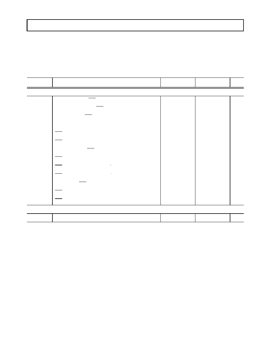
PRELIMINARY TECHNICAL DATA
This information applies to a product under development. Its characteristics and specifications are subject to change without notice. Analog
Devices assumes no obligation regarding future manufacturing unless otherwise agreed to in writing.
27
REV. PrA
For current information contact Analog Devices at (781) 937-1799
ADSP-21992
August 2002
External Port Write Cycle Timing
Table 9
and
Figure 17
describe external port write operations.
The external port lets systems extend read/write accesses in three ways: wait states, ACK input, and combined wait states
and ACK. To add waits with ACK, the DSP must see ACK low at the rising edge of EMI clock. ACK low causes the DSP
to wait, and the DSP requires two EMI clock cycles after ACK goes high to finish the access. For more information, see
the External Port chapter in the ADSP-219x/2191 DSP Hardware Reference
Table 9. External Port Write Cycle Timing
Parameter
Description
1, 2, 3
1
t
HCLK
is the peripheral clock period.
2
These are preliminary timing parameters that are based on worst case operating conditions.
3
The pad loads for these timing parameters are 20 pF.
Min
Max
Unit
Switching Characteristics
t
CWA
EMI
4
clock low to WR asserted delay
4
EMI clock is the external port clock that is generated from the EMI clock ratio. This signal is not available on an external pin, but (roughly) corresponds
to HCLK (at similar clock ratios).
2.8
ns
t
CSWS
Chip select asserted to WR de-asserted delay
4.3
6.5
ns
t
AWS
Address valid to WR setup and delay
4.9
7.0
ns
t
AKS
ACK asserted to EMI clock high delay
6.0
ns
t
WSCS
WR de-asserted to chip select de-asserted
4.8
7.0
ns
t
WSA
WR de-asserted to address invalid
4.5
6.6
ns
t
CWD
EMI clock low to WR de-asserted delay
2.5
2.7
ns
t
WW
WR strobe pulsewidth
t
HCLK
0.5
ns
t
CDA
WR to data enable access delay
1.5
4.1
ns
t
CDD
WR to data disable access delay
3.3
7.4
ns
t
DSW
Data valid to WR de-asserted setup
t
HCLK
1.4
t
HCLK
+ 4.8
ns
t
DHW
WR de-asserted to data invalid hold time; wt_hold=0
3.4
7.4
ns
t
DHW
WR de-asserted to data invalid hold time; wt_hold=1
t
HCLK
+ 3.4
t
HCLK
+ 7.4
ns
Timing Requirement
t
AKW
ACK strobe pulsewidth
10.0
ns
PRELIMINARY TECHNICAL DATA
This information applies to a product under development. Its characteristics and specifications are subject to change without notice. Analog
Devices assumes no obligation regarding future manufacturing unless otherwise agreed to in writing.
28
REV. PrA
For current information contact Analog Devices at (781) 937-1799
ADSP-21992
August 2002
Figure 17. External Port Write Cycle Timing
D150
ACK
WR
A210
MS30
IOMS
BMS
EMI CLOCK
t
CWA
t
AWS
t
CWD
t
WW
t
AK
W
t
DSW
t
DHW
t
CSWS
t
WSA
t
WSCS
t
CD
A
t
AKS
PRELIMINARY TECHNICAL DATA
This information applies to a product under development. Its characteristics and specifications are subject to change without notice. Analog
Devices assumes no obligation regarding future manufacturing unless otherwise agreed to in writing.
29
REV. PrA
For current information contact Analog Devices at (781) 937-1799
ADSP-21992
August 2002
External Port Read Cycle Timing
Table 10
and
Figure 18
describe external port read operations. For additional information on the ACK signal, see the
discussion on
on page 27
.
Table 10. External Port Read Cycle Timing
Parameter
Description
1, 2, 3
1
t
HCLK
is the peripheral clock period.
2
These are preliminary timing parameters that are based on worst case operating conditions.
3
The pad loads for these timing parameters are 20 pF.
Min
Max
Unit
Switching Characteristics
t
CRA
EMI
4
clock low to RD asserted delay
4
EMI clock is the external port clock that is generated from the EMI clock ratio. This signal is not available on an external pin, but (roughly) corresponds
to HCLK (at similar clock ratios).
2.8
ns
t
CSRS
Chip select asserted to RD asserted delay
4.3
6.5
ns
t
ARS
Address valid to RD setup and delay
4.9
7.0
ns
t
AKS
ACK asserted to EMI clock high delay
6.0
ns
t
CRD
EMI clock low to RD de-asserted delay
2.5
2.7
ns
t
RSCS
RD de-asserted to chip select de-asserted setup
4.8
7.0
ns
t
RW
RD strobe pulsewidth
t
HCLK
0.5
ns
t
RSA
RD de-asserted to address invalid setup
4.5
6.6
ns
Timing Requirements
t
AKW
ACK strobe pulsewidth
10.0
ns
t
CDA
RD to data enable access delay
0.0
ns
t
RDA
RD asserted to data access setup
t
HCLK
5.5
ns
t
ADA
Address valid to data access setup
t
HCLK
0.2
ns
t
SDA
Chip select asserted to data access setup
t
HCLK
0.6
ns
t
SD
Data valid to RD de-asserted setup
1.8
ns
t
HRD
RD de-asserted to data invalid hold
0.0
ns
PRELIMINARY TECHNICAL DATA
This information applies to a product under development. Its characteristics and specifications are subject to change without notice. Analog
Devices assumes no obligation regarding future manufacturing unless otherwise agreed to in writing.
30
REV. PrA
For current information contact Analog Devices at (781) 937-1799
ADSP-21992
August 2002
Figure 18. External Port Read Cycle Timing
D150
ACK
RD
A210
MS30
IOMS
BMS
EMI CLOCK
t
CRA
t
ARS
t
CRD
t
RW
t
AKW
t
CDA
t
RDA
t
ADA
t
SDA
t
SD
t
HRD
t
CSRS
t
RSA
t
RSCS
t
AKS
PRELIMINARY TECHNICAL DATA
This information applies to a product under development. Its characteristics and specifications are subject to change without notice. Analog
Devices assumes no obligation regarding future manufacturing unless otherwise agreed to in writing.
31
REV. PrA
For current information contact Analog Devices at (781) 937-1799
ADSP-21992
August 2002
External Port Bus Request and Grant Cycle Timing
Table 11
and
Figure 19
describe external port bus request and bus grant operations.
Table 11. External Port Bus Request and Grant Cycle Timing
Parameter
Description
1, 2, 3
1
t
HCLK
is the peripheral clock period.
2
These are preliminary timing parameters that are based on worst case operating conditions.
3
The pad loads for these timing parameters are 20 pF.
Min
Max
Unit
Switching Characteristics
t
SD
CLKOUT high to xMS, address, and RD/WR disable
4.3
ns
t
SE
CLKOUT low to xMS, address, and RD/WR enable
4.0
ns
t
DBG
CLKOUT high to BG asserted setup
2.2
ns
t
EBG
CLKOUT high to BG de-asserted hold time
2.2
ns
t
DBH
CLKOUT high to BGH asserted setup
2.4
ns
t
EBH
CLKOUT high to BGH de-asserted hold time
2.4
ns
Timing Requirements
t
BS
BR asserted to CLKOUT high setup
4.6
ns
t
BH
CLKOUT high to BR de-asserted hold time
0.0
ns
PRELIMINARY TECHNICAL DATA
This information applies to a product under development. Its characteristics and specifications are subject to change without notice. Analog
Devices assumes no obligation regarding future manufacturing unless otherwise agreed to in writing.
32
REV. PrA
For current information contact Analog Devices at (781) 937-1799
ADSP-21992
August 2002
Figure 19. External Port Bus Request and Grant Cycle Timing
t
BH
BR
A210
MS30
IOMS
BMS
CLKOUT
BG
WR
RD
BGH
t
BS
t
SD
t
SD
t
SD
t
DBG
t
DBH
t
SE
t
SE
t
SE
t
EBG
t
EBH

PRELIMINARY TECHNICAL DATA
This information applies to a product under development. Its characteristics and specifications are subject to change without notice. Analog
Devices assumes no obligation regarding future manufacturing unless otherwise agreed to in writing.
33
REV. PrA
For current information contact Analog Devices at (781) 937-1799
ADSP-21992
August 2002
Serial Port (SPORT) Clocks and Data Timing
Table 12
and
Figure 20
describe SPORT transmit and receive operations.
Table 12. Serial Port (SPORT) Clocks and Data Timing
1
1
To determine whether communication is possible between two devices at clock speed n, the following specifications must be confirmed:
1) frame sync delay and frame sync setup and hold, 2) data delay and data setup and hold, and 3) SCLK width.
Parameter
Description
Min
Max
Unit
Switching Characteristics
t
HOFSE
RFS Hold after RCLK (Internally Generated RFS)
2
2
Referenced to drive edge.
0
12.4
ns
t
DFSE
RFS Delay after RCLK (Internally Generated RFS)
2
0
12.4
ns
t
DDTEN
Transmit Data Delay after TCLK
2
0
12.1
ns
t
DDTTE
Data Disable from External TCLK
2
0
12.0
ns
t
DDTIN
Data Enable from Internal TCLK
2
0
6.8
ns
t
DDTTI
Data Disable from Internal TCLK
2
0
6.3
ns
Timing Requirements
t
SCLKIW
TCLK/RCLK Width
20
ns
t
SFSI
TFS/RFS Setup before TCLK/RCLK
3
3
Referenced to sample edge.
0.6
ns
t
HFSI
TFS/RFS Hold after TCLK/RCLK
3, 4
4
RFS hold after RCLK when MCE = 1, MFD = 0 is 0 ns minimum from drive edge. TFS hold after TCLK for late external TFS is 0 ns minimum from
drive edge.
0.3
ns
t
SDRI
Receive Data Setup before RCLK
3
2.3
ns
t
HDRI
Receive Data Hold after RCLK
3
1.9
ns
t
SCLKW
TCLK/RCLK Width
20
ns
t
SFSE
TFS/RFS Setup before TCLK/RCLK
3
0.6
ns
t
HFSE
TFS/RFS Hold after TCLK/RCLK
3, 4
0.6
ns
t
SDRE
Receive Data Setup before RCLK
3
2.2
ns
t
HDRE
Receive Data Hold after RCLK
3
1.8
ns
PRELIMINARY TECHNICAL DATA
This information applies to a product under development. Its characteristics and specifications are subject to change without notice. Analog
Devices assumes no obligation regarding future manufacturing unless otherwise agreed to in writing.
34
REV. PrA
For current information contact Analog Devices at (781) 937-1799
ADSP-21992
August 2002
Figure 20. Serial Port (SPORT) Clocks and Data
DRIVE EDGE
DRIVE EDGE
SCLK
t
DDTEN
t
DDTTE
SCLK
(INT)
SCLK
(EXT)
SCLK
FS
DRIVE
EDGE
SAMPLE
EDGE
DATA RECEIVE-- EXTERNAL CLOCK
DXA/DXB
t
SCLKW
TDFSE
t
HOFSE
t
SFSE
t
HFSE
t
SDRE
t
HDRE
NOTE: EITHER THE RISING EDGE OR FALLING EDGE OF SCLK (EXTERNAL), SCLK (INTERNAL) CAN BE USED AS THE ACTIVE SAMPLING EDGE.
DXA/DXB
DXA/DXB
SCLK
FS
DRIVE
EDGE
SAMPLE
EDGE
DATA RECEIVE-- INTERNAL CLOCK
DXA/DXB
t
SCLKIW
t
DFSE
t
HOFSE
t
SFSI
t
HFSI
t
SDRI
t
HDRI
SCLK
t
DDTIN
t
DDTTI
DRIVE EDGE
DRIVE EDGE

PRELIMINARY TECHNICAL DATA
This information applies to a product under development. Its characteristics and specifications are subject to change without notice. Analog
Devices assumes no obligation regarding future manufacturing unless otherwise agreed to in writing.
35
REV. PrA
For current information contact Analog Devices at (781) 937-1799
ADSP-21992
August 2002
Serial Port (SPORT) Frame Synch Timing
Table 13
and
Figure 21
describe SPORT frame synch operations.
To determine whether communication is possible between two devices at clock speed n, the following specifications must
be confirmed: 1) frame sync delay and frame sync setup and hold, 2) data delay and data setup and hold, and 3)
R/TCLK width.
Table 13. Serial Port (SPORT) Frame Synch Timing
Parameter
Description
Min
Max
Unit
Switching Characteristics
t
HOFSE
RFS Hold after RCLK (Internally Generated RFS)
1
1
Referenced to drive edge.
12.4
ns
t
HOFSI
TFS Hold after TCLK (Internally Generated TFS)
1
12.2
ns
t
DDTENFS
Data Enable from late FS or MCE = 1, MFD = 0
2
2
MCE = 1, TFS enable and TFS valid follow t
DDTLFSE
and t
DDTENFS
.
4.7
ns
t
DDTLFSE
Data Delay from Late External TFS or External RFS with
MCE = 1, MFD = 0
3
4.7
ns
t
HDTE
Transmit Data Hold after TCLK (external clk)
1
12.4
ns
t
HDTI
Transmit Data Hold after TCLK (internal clk)
1
0
12.2
ns
t
DDTE
Transmit Data Delay after TCLK (external clk)
1
0
12.2
ns
t
DDTI
Transmit Data Delay after TCLK (internal clk)
1
0
11.1
ns
Timing Requirements
t
SFSE
TFS/RFS Setup before TCLK/RCLK (external clk)
3
3
Referenced to sample edge.
0.6
TBD
ns
t
SFSI
TFS/RFS Setup before TCLK/RCLK (internal clk)
3
0.6
TBD
ns
PRELIMINARY TECHNICAL DATA
This information applies to a product under development. Its characteristics and specifications are subject to change without notice. Analog
Devices assumes no obligation regarding future manufacturing unless otherwise agreed to in writing.
36
REV. PrA
For current information contact Analog Devices at (781) 937-1799
ADSP-21992
August 2002
Figure 21. Serial Port (SPORT) Frame Synch
DRIVE
SAMPLE
DRIVE
FIRST BIT
SECOND BIT
SCLK
FS
t
HOFSE/I
t
DDTENFS
t
DDTLFSE
t
SFSE/I
LATE EXTERNAL TRANSMIT FS
EXTERNAL RECEIVE FS WITH MCE = 1, MFD = 0
DRIVE
SAMPLE
DRIVE
FIRST BIT
SECOND BIT
SCLK
FS
t
HOFSE/I
t
DDTENFS
t
DDTLFSE
DXA/DXB
t
SFSE/I
t
DDTE/I
t
HDTE/I
t
DDTE/I
t
HDTE/I
DXA/DXB

PRELIMINARY TECHNICAL DATA
This information applies to a product under development. Its characteristics and specifications are subject to change without notice. Analog
Devices assumes no obligation regarding future manufacturing unless otherwise agreed to in writing.
37
REV. PrA
For current information contact Analog Devices at (781) 937-1799
ADSP-21992
August 2002
Serial Peripheral Interface (SPI) Port--Master Timing
Table 14
and
Figure 22
describe SPI port master operations.
Table 14. Serial Peripheral Interface (SPI) Port--Master Timing
Parameter
Description
Min
Max
Unit
Switching Characteristics
t
SDSCIM
SPISS low to first SCLK edge
2t
HCLK
ns
t
SPICHM
Serial clock high period
2t
HCLK
ns
t
SPICLM
Serial clock low period
2t
HCLK
ns
t
SCK
Serial clock period
4t
HCLK
ns
t
HDSM
Last SCLK edge to SPISS high
2t
HCLK
ns
t
SPITDM
Sequential transfer delay
2t
HCLK
ns
t
DDSPID
SCLK edge to data out valid (data out delay)
0
6
ns
t
HDSPID
SCLK edge to data out invalid (data out hold)
0
5
ns
Timing Requirements
t
SSPID
Data input valid to SCLK edge (data input setup)
1.6
ns
t
HSPID
SCLK sampling edge to data input invalid
1.6
ns
PRELIMINARY TECHNICAL DATA
This information applies to a product under development. Its characteristics and specifications are subject to change without notice. Analog
Devices assumes no obligation regarding future manufacturing unless otherwise agreed to in writing.
38
REV. PrA
For current information contact Analog Devices at (781) 937-1799
ADSP-21992
August 2002
Figure 22. Serial Peripheral Interface (SPI) Port--Master
t
SSPID
t
HSPID
t
HDSPID
LSB
MSB
THSPID
t
DDS-
PID
MOSI
(OUTPUT)
MISO
(INPUT)
SPISS
(OUTPUT)
SCLK
(CPOL = 0)
(OUTPUT)
SCLK
(CPOL = 1)
(OUTPUT)
MOSI
(OUTPUT)
MISO
(INPUT)
CPHA=1
CPHA=0
t
SPICHM
t
SPICLM
t
SPICLM
t
SPICLK
t
SPICHM
t
HDSM
t
SPITDM
t
HDSPID
LSB
VALID
LSB
MSB
MSB
VALID
THSPID
t
DDS-
PID
t
SSPID
MSB
VALID
t
SDSCIM
t
SSPID
LSB
VALID
PRELIMINARY TECHNICAL DATA
This information applies to a product under development. Its characteristics and specifications are subject to change without notice. Analog
Devices assumes no obligation regarding future manufacturing unless otherwise agreed to in writing.
39
REV. PrA
For current information contact Analog Devices at (781) 937-1799
ADSP-21992
August 2002
Serial Peripheral Interface (SPI) Port--Slave Timing
Table 15
and
Figure 23
describe SPI port slave operations.
Table 15. Serial Peripheral Interface (SPI) Port--Slave Timing
Parameter
Description
Min
Max
Unit
Switching Characteristics
t
DSOE
SPISS assertion to data out active
0
6
ns
t
DSDHI
SPISS deassertion to data high impedance
0
6
ns
t
DDSPID
SCLK edge to data out valid (data out delay)
0
5
ns
t
HDSPID
SCLK edge to data out invalid (data out hold)
0
5
ns
Timing Requirements
t
SPICHS
Serial clock high period
2t
HCLK
ns
t
SPICLS
Serial clock low period
2t
HCLK
ns
t
SCK
Serial clock period
4t
HCLK
ns
t
HDS
Last SCK edge to SPISS not asserted
2t
HCLK
ns
t
SPITDS
Sequential Transfer Delay
2t
HCLK
ns
t
SDSCI
SPISS assertion to first SCK edge
2t
HCLK
ns
t
SSPID
Data input valid to SCLK edge (data input setup)
1.6
ns
t
HSPID
SCLK sampling edge to data input invalid
1.6
ns
PRELIMINARY TECHNICAL DATA
This information applies to a product under development. Its characteristics and specifications are subject to change without notice. Analog
Devices assumes no obligation regarding future manufacturing unless otherwise agreed to in writing.
40
REV. PrA
For current information contact Analog Devices at (781) 937-1799
ADSP-21992
August 2002
Figure 23. Serial Peripheral Interface (SPI) Port--Slave
t
HSPID
t
DDSPID
t
DSDHI
LSB
MSB
MSB
VALID
t
HSPID
t
DSOE
t
DDSPID
t
HDSPID
MISO
(OUTPUT)
MOSI
(INPUT)
SPISS
(INPUT)
SCLK
(CPOL = 0)
(INPUT)
SCLK
(CPOL = 1)
(INPUT)
MISO
(OUTPUT)
MOSI
(INPUT)
CPHA=1
CPHA=0
TSSPID
t
SDSCI
t
SPICHS
t
SPICLS
t
SPICLS
t
SPICLK
t
HDS
t
SPICHS
t
SSPID
t
HSPID
t
DSDHI
LSB
VALID
MSB
MSB
VALID
t
DSOE
t
DDSPID
t
SSPID
LSB
VALID
LSB
TSPITD
S
PRELIMINARY TECHNICAL DATA
This information applies to a product under development. Its characteristics and specifications are subject to change without notice. Analog
Devices assumes no obligation regarding future manufacturing unless otherwise agreed to in writing.
41
REV. PrA
For current information contact Analog Devices at (781) 937-1799
ADSP-21992
August 2002
JTAG Test And Emulation Port Timing
Table 16
and
Figure 24
describe JTAG port operations.
Table 16. JTAG Port Timing
Parameter
Description
Min
Max
Unit
Switching Characteristics
t
DTDO
TDO Delay from TCK Low
4
ns
t
DSYS
System Outputs Delay After TCK Low
1
1
System Outputs = DATA150, ADDR210, MS30, RD, WR, ACK, CLKOUT, BG, PF70, TIMEXP, DT, DT1, TCLK, TCLK1, RCLK, RCLK1,
TFS, TFS1, RFS, RFS1, BMS.
0
5
ns
Timing Parameters
t
TCK
TCK Period
20
ns
t
STAP
TDI, TMS Setup Before TCK High
4
ns
t
HTAP
TDI, TMS Hold After TCK High
4
ns
t
SSYS
System Inputs Setup Before TCK Low
2
2
System Inputs = DATA150, ADDR210, RD, WR, ACK, BR, BG, PF70, DR, DR1, TCLK, TCLK1, RCLK, RCLK1, TFS, TFS1, RFS, RFS1,
CLKIN, RESET.
4
ns
t
HSYS
System Inputs Hold After TCK Low
2
5
ns
t
TRSTW
TRST Pulsewidth
3
3
50 MHz max.
4
ns
Figure 24. JTAG Port Timing
TMS
TDI
TDO
SYSTEM
INPUTS
SYSTEM
OUTPUTS
TCK
t
TCK
t
HTAP
t
STAP
t
DTDO
t
SSYS
t
HSYS
t
DSYS
This information applies to a product under development. Its characteristics and specifications are subject to change without notice. Analog
Devices assumes no obligation regarding future manufacturing unless otherwise agreed to in writing.
42
REV. PrA
For current information contact Analog Devices at (781) 937-1799
ADSP-21992
August 2002
PRELIMINARY TECHNICAL DATA
Output Drive Currents
Figure 25
shows typical current and voltage characteristics
for the output drivers of the ADSP-21992. The curves
represent the current drive capability of the output drivers
as a function of output voltage.
Power Dissipation
Total power dissipation has two components, one due to
internal circuitry and one due to the switching of external
output drivers. Internal power dissipation is dependent on
the instruction execution sequence and the data operands
involved. Using the current specifications (I
DDINPEAK
, I
DDINHIGH
,
I
DDINLOW
, I
DDIDLE
) from the
Electrical Characteristics on
page 22
and the current versus operation information in
Table 17
, designers can estimate the ADSP-21992's
internal power supply (V
DDINT
) input current for a specific
application, according to the formula in
Figure 26
.
The external component of total power dissipation is caused
by the switching of output pins. Its magnitude depends on:
·
The number of output pins that switch during each cycle
(O)
·
The maximum frequency at which they can switch (f)
·
Their load capacitance (C)
·
Their voltage swing (V
DD
)
and is calculated by the formula in
Figure 27
.
The load capacitance should include the processor's
package capacitance (C
IN
). The switching frequency
includes driving the load high and then back low. Address
and data pins can drive high and low at a maximum rate of
1
/
(2t
CK
). The write strobe can switch every cycle at a
frequency of 1
/
t
CK
. Select pins switch at 1
/
(2t
CK
), but selects
can switch on each cycle. For example, estimate P
EXT
with
the following assumptions:
·
A system with one bank of external data memory--asyn-
chronous RAM (16-bit)
·
Four 8K 16 RAM chips are used, each with a load of 10
pF
·
External data memory writes occur every other cycle, a
rate of 1
/
(4t
CK
), with 50% of the pins switching
·
The bus cycle time is 50 MHz (t
CK
= 20 ns)
Figure 25. ADSP-21992 Typical Drive Currents
SOURCE (V
DDEXT
) VOLTAGE V
120
100
80
60
40
20
0
20
40
60
80
100
120
0
3.5
0.5
1
1.5
2.0
2.5
3.0
S
O
U
R
C
E
(
V
D
D
E
X
T
)
C
U
R
R
E
N
T
M
A
TBD
Table 17. ADSP-21992 Operation Types Versus Input Current
Operation
Typical Activity (I
DD TYPICAL
)
High Activity (I
DD IDLE
)
Low Activity (I
DD PWRDWN
)
Instruction Type
TBD
TBD
TBD
Instruction Fetch
TBD
TBD
TBD
Core Memory Access
1
TBD
TBD
TBD
Internal Memory DMA
TBD
TBD
TBD
External Memory
DMA
TBD
TBD
TBD
Data bit pattern for core
memory access and
DMA
TBD
TBD
TBD
1
These assume a 2:1 core clock ratio. For more information on ratios and clocks (t
CK
and t
CCLK
), see
Clock Signals on page 13
.
Figure 26. I
DDINT
Calculation
I
DDINT
%Typical
I
DD-TYPICAL
×
(
)
=
%Idle
I
DD-IDLE
×
(
)
%Powerdown
I
DD-PWRDWN
×
(
)
+
+
Figure 27. P
EXT
Calculation
P
EXT
O
C
×
V
DD
2
×
f
×
=
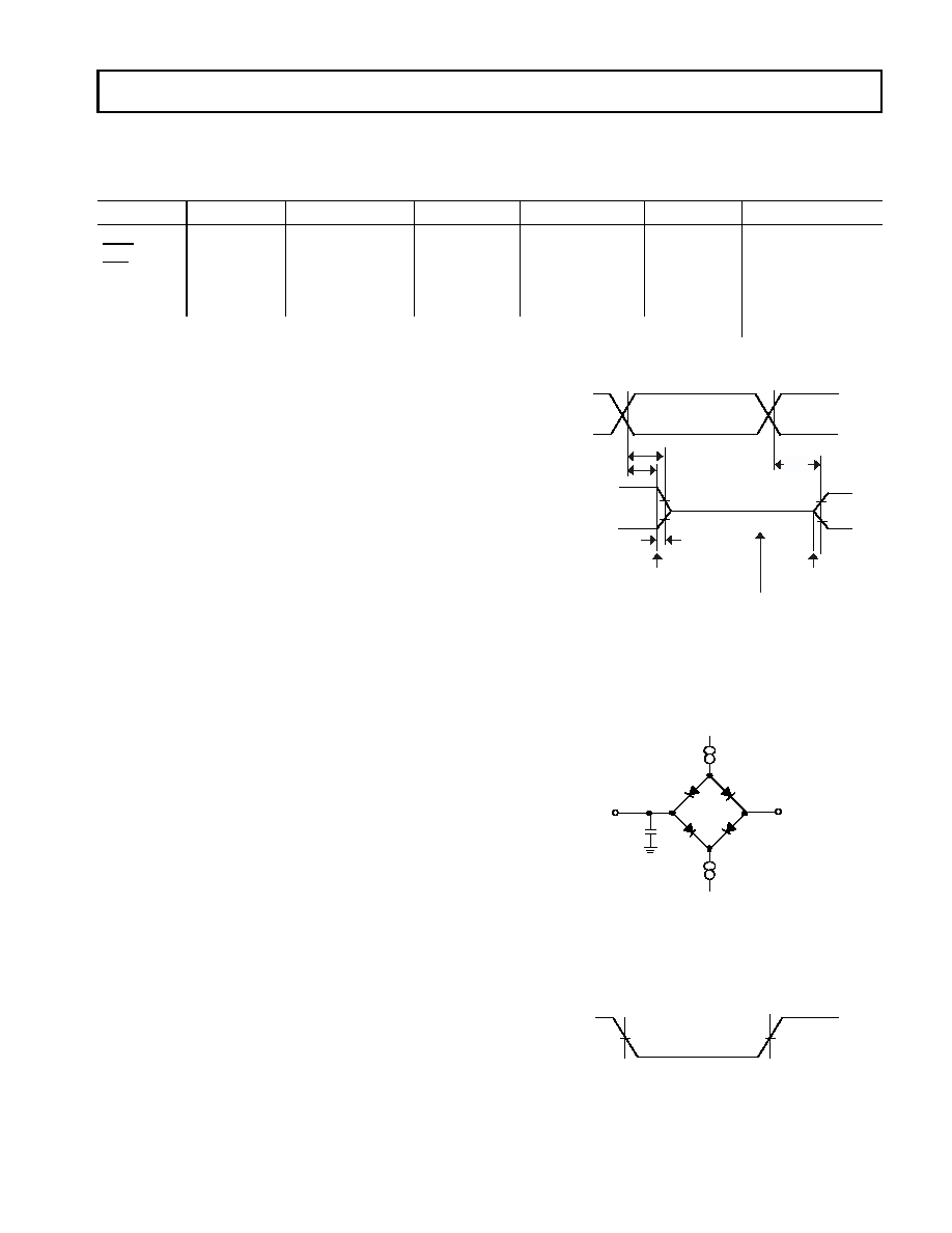
This information applies to a product under development. Its characteristics and specifications are subject to change without notice. Analog
Devices assumes no obligation regarding future manufacturing unless otherwise agreed to in writing.
43
REV. PrA
For current information contact Analog Devices at (781) 937-1799
ADSP-21992
August 2002
PRELIMINARY TECHNICAL DATA
The P
EXT
equation is calculated for each class of pins that
can drive as shown in
Table 18
.
A typical power consumption can now be calculated for
these conditions by adding a typical internal power dissipa-
tion with the formula in
Figure 28
.
Where:
·
P
EXT
is from
Table 18
·
P
INT
is I
DDINT
2.5V, using the calculation I
DDINT
listed in
Power Dissipation on page 42
Note that the conditions causing a worst case P
EXT
are
different from those causing a worst case P
INT
. Maximum
P
INT
cannot occur while 100% of the output pins are
switching from all ones to all zeros. Note also that it is not
common for an application to have 100% or even 50% of
the outputs switching simultaneously.
Test Conditions
The DSP is tested for output enable, disable, and hold time.
Output Disable Time
Output pins are considered to be disabled when they stop
driving, go into a high impedance state, and start to decay
from their output high or low voltage. The time for the
voltage on the bus to decay by V is dependent on the
capacitive load, C
L
and the load current, I
L
. This decay time
can be approximated by the equation in
Figure 29
.
The output disable time t
DIS
is the difference between
t
MEASURED
and t
DECAY
as shown in
Figure 30
. The time t
MEASURED
is the interval from when the reference signal switches to
when the output voltage decays V from the measured
output high or output low voltage. The t
DECAY
is calculated
with test loads C
L
and I
L
, and with V equal to 0.5 V.
Table 18. P
EXT
Calculation
Pin Type
# of Pins
% Switching
C
f
V
DD
2
= P
EXT
Address
15
50
44.7 pF
12.5 MHz
10.9 V
= 0.046 W
MSx
1
0
44.7 pF
12.5 MHz
10.9 V
= 0.000 W
WR
2
100
44.7 pF
25 MHz
10.9 V
= 0.024 W
Data
64
50
14.7 pF
12.5 MHz
10.9 V
= 0.064 W
CLKOUT
1
100
4.7 pF
25 MHz
10.9 V
= 0.001 W
P
EXT
= 0.135 W
Figure 28. P
TOTAL
(Typical) Calculation
Figure 29. Decay Time Calculation
P
TOTAL
P
=
EXT
P
INT
+
t
DECAY
C
L
V
I
L
---------------
=
Figure 30. Output Enable/Disable
Figure 31. Equivalent Device Loading for AC
Measurements (Includes All Fixtures)
Figure 32. Voltage Reference Levels for AC
Measurements (Except Output Enable/Disable)
REFERENCE
SIGNAL
t
DIS
OUTPUT STARTS
DRIVING
V
OH
(MEASURED) DV
V
OL
(MEASURED) + DV
t
MEASURED
V
OH
(MEASURED)
V
OL
(MEASURED)
2.0V
1.0V
HIGH-IMPEDANCE STATE.
TEST CONDITIONS CAUSE THISVOLT-
AGE TO BE APPROXIMATELY 1.5V
OUTPUT STOPS
DRIVING
t
DECAY
t
ENA
+1.5V
50PF
TO
OUTPUT
PIN
IOL
IOH
INPUT
OR
OUTPUT
1.5V
1.5V

This information applies to a product under development. Its characteristics and specifications are subject to change without notice. Analog
Devices assumes no obligation regarding future manufacturing unless otherwise agreed to in writing.
44
REV. PrA
For current information contact Analog Devices at (781) 937-1799
ADSP-21992
August 2002
PRELIMINARY TECHNICAL DATA
Output Enable Time
Output pins are considered to be enabled when they have
made a transition from a high impedance state to when they
start driving. The output enable time t
ENA
is the interval from
when a reference signal reaches a high or low voltage level
to when the output has reached a specified high or low trip
point, as shown in the Output Enable/Disable diagram
(
Figure 30
). If multiple pins (such as the data bus) are
enabled, the measurement value is that of the first pin to
start driving.
Example System Hold Time Calculation
To determine the data output hold time in a particular
system, first calculate t
DECAY
using the equation given in
Figure 29
. Choose V to be the difference between the
ADSP-21992's output voltage and the input threshold for
the device requiring the hold time. A typical V will be 0.4 V.
C
L
is the total bus capacitance (per data line), and I
L
is the
total leakage or three state current (per data line). The hold
time will be t
DECAY
plus the minimum disable time (i.e.,
t
DATRWH
for the write cycle).
Capacitive Loading
Output delays and holds are based on standard capacitive
loads: 50 pF on all pins (see
Figure 35
). The delay and hold
specifications given should be derated by a factor of
1.5 ns/50 pF for loads other than the nominal value of
50 pF.
Figure 33
and
Figure 34
show how output rise time
varies with capacitance. These figures also show graphically
how output delays and holds vary with load capacitance.
(Note that this graph or derating does not apply to output
disable delays; see
Output Disable Time on page 43
.) The
graphs in these figures may not be linear outside the ranges
shown.
Environmental Conditions
The thermal characteristics in which the DSP is operating
influence performance.
Thermal Characteristics
The ADSP-21992 comes in a 196-lead Ball Grid Array
(mini-BGA) package. The ADSP-21992 is specified for an
ambient temperature (T
AMB
) as calculated using the formula
in
Figure 36
. To ensure that the T
AMB
data sheet specification
is not exceeded, a heatsink and/or an air flow source may be
used. A heatsink should be attached to the ground plane (as
close as possible to the thermal pathways) with a thermal
adhesive.
Figure 33. Typical Output Rise Time (10%90%,
V
DDEXT
=Max) vs. Load Capacitance
LOAD CAPACITANCEPF
16.0
8.0
0
0
200
20
40
60
80
100
120
140
160
180
14.0
12.0
4.0
2.0
10.0
6.0
TBD
R
I
S
E
A
N
D
F
A
L
L
T
I
M
E
S
N
S
(
0
.
3
5
V
3
.
1
2
V
,
1
0
%
9
0
%
)
Figure 34. Typical Output Rise Time (10%-90%,
V
DDEXT
=Min) vs. Load Capacitance
Figure 35. Typical Output Delay or Hold vs. Load
Capacitance (at Max Case Temperature)
Figure 36. T
CASE
Calculation
3.5
0
3.0
2.5
2.0
1.5
1.0
0.5
LOAD CAPACITANCEPF
0
200
20
40
60
80
100
120
140
160
180
TBD
R
I
S
E
A
N
D
F
A
L
L
T
I
M
E
S
N
S
(
0
.
3
1
2
.
8
2
,
1
0
%
9
0
%
)
LOAD CAPACITANCEPF
5
25
50
75
100
125
150
175
4
3
2
1
TBD
O
U
T
P
U
T
D
E
L
A
Y
O
R
H
O
L
D
N
S
NOMINAL
T
AMB
T
CASE
=
PD
CA
×

This information applies to a product under development. Its characteristics and specifications are subject to change without notice. Analog
Devices assumes no obligation regarding future manufacturing unless otherwise agreed to in writing.
45
REV. PrA
For current information contact Analog Devices at (781) 937-1799
ADSP-21992
August 2002
PRELIMINARY TECHNICAL DATA
Where:
·
T
AMB
= Ambient temperature (measured near top surface
of package)
·
PD = Power dissipation in W (this value depends upon
the specific application; a method for calculating PD is
shown under Power Dissipation).
·
CA
= Value from
Table 19
.
·
JB
= TBD°C
/
W
There are some important things to note about these T
AMB
calculations and the values in
Table 19
:
·
This represents thermal resistance at total power of
TBD W.
·
For the mini-BGA package:
JC
= 8.4°C
/
W
ADSP-21992 Pinout
Table 20
identifies the signal for each LQFP lead number.
Table 21
identifies the LQFP lead number for each signal
name.
Table 5
describes each signal.
Table 19.
CA
Values
1
1
These are preliminary estimates.
Airflow
(Linear Ft.
/
Min.)
0
100
200
400
600
Airflow
(Meters
/
Second)
0
0.5
1
2
3
Mini-BGA:
CA
(°C
/
W)
26
24
22
20.9
19.8
This information applies to a product under development. Its characteristics and specifications are subject to change without notice. Analog
Devices assumes no obligation regarding future manufacturing unless otherwise agreed to in writing.
46
REV. PrA
For current information contact Analog Devices at (781) 937-1799
ADSP-21992
August 2002
PRELIMINARY TECHNICAL DATA
Table 20. 176-lead LQFP
Signal By Lead Number
Lead #
Signal
Lead #
Signal
Lead #
Signal
Lead #
Signal
1
N/C
45
VDDEXT
89
N/C
133
VDDEXT
2
N/C
46
A4
90
N/C
134
PF11
3
VDDEXT
47
A3
91
VDDEXT
135
PF10
4
RCLK
48
A2
92
BYPASS
136
PF9
5
SCK
49
A1
93
BMODE0
137
PF8
6
MISO
50
A0
94
BMODE1
138
PF7/SPISEL7
7
MOSI
51
D15
95
BMODE2
139
PF6/SPISEL6
8
RD
52
D14
96
N/C
140
PF5/SPISEL5
9
WR
53
D13
97
DGND
141
PF4/SPISEL4
10
ACK
54
D12
98
VDDINT
142
DGND
11
BR
55
D11
99
EMU
143
VDDEXT
12
BG
56
DGND
100
TRST
144
PF3/SPISEL3
13
BGH
57
VDDEXT
101
TDO
145
PF2/SPISEL2
14
IOMS
58
DGND
102
TDI
146
PF1/SPISEL1
15
BMS
59
VDDINT
103
TMS
147
PF0/SPISS0
16
MS3
60
D10
104
TCK
148
DGND
17
DGND
61
D9
105
POR
149
VDDINT
18
VDDEXT
62
D8
106
RESET
150
AVSS
19
MS2
63
D7
107
CLKIN
151
AVDD
20
MS1
64
D6
108
XTAL
152
N/C
21
MS0
65
D5
109
CLKOUT
153
VREF
22
DGND
66
DGND
110
CONVST
154
CML
23
VDDINT
67
VDDINT
111
TMR0
155
CAPT
24
A19
68
D4
112
DGND
156
CAPB
25
A18
69
D3
113
VDDEXT
157
SENSE
26
A17
70
D2
114
TMR1
158
VIN3
27
A16
71
D1
115
TMR2
159
VIN2
28
A15
72
D0
116
EIS
160
VIN1
29
A14
73
CANRX
117
DGND
161
VIN0
30
A13
74
DGND
118
VDDINT
162
ASHAN
31
DGND
75
VDDEXT
119
EIZ
163
BSHAN
32
VDDEXT
76
CL
120
EIB
164
VIN4
33
A12
77
CH
121 EIA
165
VIN5
34
A11
78
BL
122
AUXTRIP
166
VIN6
35
A10
79
BH
123
AUX1
167
VIN7
36
A9
80
AL
124
AUX0
168
AVSS
37
A8
81
AH
125
PF15
169
AVDD
38
A7
82
CANTX
126
PF14
170
DT
39
A6
83 N/C
127
PF13
171
DR
40
A5
84
PWMSYNC
128
PF12
172
RFS
41
DGND
85 PWMPOL
129
DGND
173
TFS
42
N/C
86 PWMSR
130
N/C
174
TCLK
43
N/C
87
PWMTRIP
131
N/C
175
DGND
44
N/C
88
DGND
132
N/C
176
N/C
This information applies to a product under development. Its characteristics and specifications are subject to change without notice. Analog
Devices assumes no obligation regarding future manufacturing unless otherwise agreed to in writing.
47
REV. PrA
For current information contact Analog Devices at (781) 937-1799
ADSP-21992
August 2002
PRELIMINARY TECHNICAL DATA
Table 21. 176-lead LQFP
Lead Number by Signal
Signal
Lead #
Signal
Lead #
Signal
Lead #
Signal
Lead #
A0
50
CAPB
156
EIS
116
PWMTRIP
87
A1
49
CAPT
155
EIZ
119
RCLK
4
A10
35
CH
77
EMU
99
RD
8
A11
34
CL
76
IOMS
14
RESET
106
A12
33
CLKIN
107
MISO
6
RFS
172
A13
30
CLKOUT
109
MOSI
7
SCK
5
A14
29
CML
154
MS0
21
SENSE
157
A15
28
CONVST
110
MS1
20
TCK
104
A16
27
D0
72
MS2
19
TCLK
174
A17
26
D1
71
MS3
16
TDI
102
A18
25
D10
60
N/C
1
TDO
101
A19
24
D11
55
N/C
2
TFS
173
A2
48
D12
54
N/C
42
TMR0
111
A3
47
D13
53
N/C
43
TMR1
114
A4
46
D14
52
N/C
44
TMR2
115
A5
40
D15
51
N/C
83
TMS
103
A6
39
D2
70
N/C
89
TRST
100
A7
38
D3
69
N/C
90
VDDEXT
3
A8
37
D4
68
N/C
96
VDDEXT
18
A9
36
D5
65
N/C
130
VDDEXT
32
ACK
10
D6
64
N/C
131
VDDEXT
45
AH
81
D7
63
N/C
132
VDDEXT
57
AL
80
D8
62
N/C
152
VDDEXT
75
ASHAN
162
D9
61
N/C
176
VDDEXT
91
AUX0
124
DGND
17
PF0/SPISS0
147
VDDEXT
113
AUX1
123
DGND
22
PF1/SPISEL1
146
VDDEXT
133
AUXTRIP
122
DGND
31
PF10
135
VDDEXT
143
AVDD
151
DGND
41
PF11
134
VDDINT
23
AVDD
169
DGND
56
PF12
128
VDDINT
59
AVSS
150
DGND
58
PF13
127
VDDINT
67
AVSS
168
DGND
66
PF14
126
VDDINT
98
BG
12
DGND
74
PF15
125
VDDINT
118
BGH
13
DGND
88
PF2/SPISEL2
145
VDDINT
149
BH
79
DGND
97
PF3/SPISEL3
144
VIN0
161
BL
78
DGND
112
PF4/SPISEL4
141
VIN1
160
BMODE0
93
DGND
117
PF5/SPISEL5
140
VIN2
159
BMODE1
94
DGND
129
PF6/SPISEL6
139
VIN3
158
BMODE2
95
DGND
142
PF7/SPISEL7
138
VIN4
164
BMS
15
DGND
148
PF8
137
VIN5
165
BR
11
DGND
175
PF9
136
VIN6
166
BSHAN
163
DR
171
POR
105
VIN7
167
BYPASS
92
DT
170
PWMPOL
85 VREF
153
CANRX
73
EIA
121
PWMSR
86 WR
9
CANTX
82
EIB
120
PWMSYNC
84 XTAL
108
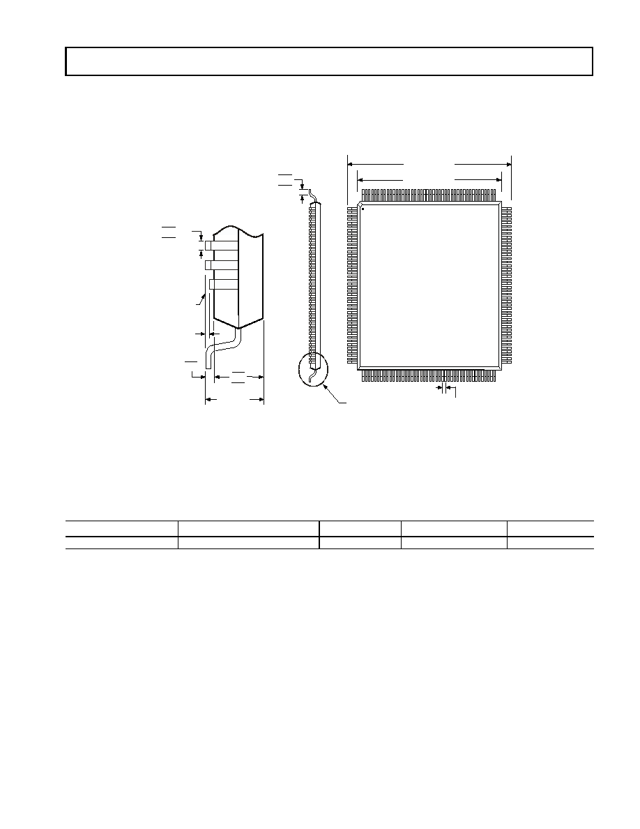
This information applies to a product under development. Its characteristics and specifications are subject to change without notice. Analog
Devices assumes no obligation regarding future manufacturing unless otherwise agreed to in writing.
48
REV. PrA
For current information contact Analog Devices at (781) 937-1799
ADSP-21992
August 2002
PRELIMINARY TECHNICAL DATA
OUTLINE DIMENSIONS
Dimensions in the outline diagram are shown in millimeters.
ORDERING GUIDE
176-LEAD LQFP (ST-176-1)
Part Number
Ambient Temperature Range
Instruction Rate Operating Voltage
Package
ADSP-21992YST
40ºC to +115ºC
160 MHz
2.5 Int./3.3 Ext. V
176-lead LQFP
TOP VIEW (PINS DOWN)
PIN 1
133
1
132
45
44
88
89
176
26.00
BSC SQ
24.00 BSC SQ
0.27
0.22 TYP
0.17
0.50 BSC
LEAD PITCH
0.75
0.60
0.45
SEATING
PLANE
1.60 MAX
0.15
0.05
0.08 MAX LEAD
COPLANARITY
1.45
1.40
1.35
DETAIL A
NOTES:
1.
DIMENSIONS IN MILLIMETERS.
2.
ACTUAL POSITION OF EACH LEAD IS WITHIN 0.08 OF ITS
IDEAL POSITION, WHEN MEASURED IN THE LATERAL DIRECTION.
3.
CENTER DIMENSIONS ARE NOMINAL.
DETAIL A

This datasheet has been download from:
www.datasheetcatalog.com
Datasheets for electronics components.
Document Outline