Äîêóìåíòàöèÿ è îïèñàíèÿ www.docs.chipfind.ru
±1°C Temperature Monitor with
Series Resistance Cancellation
ADT7461*
FEATURES
On-chip and remote temperature sensor
0.25°C resolution/1°C accuracy on remote channel
1°C resolution/3°C accuracy on local channel
Automatically cancels up to 3 k (typ) of resistance in series
with remote diode to allow noise filtering
Extended, switchable temperature measurement range 0°C
to +127°C (default) or 55°C to +150°C
Pin and register compatible with ADM1032
2-wire SMBus serial interface with SMBus alert support
Programmable over/under temperature limits
Offset registers for system calibration
Up to 2 overtemperature fail-safe THERM outputs
Small 8-lead SOIC or MSOP package
170 µA operating current, 5.5 µA standby current
APPLICATIONS
Desktop and notebook computers
Industrial controllers
Smart batteries
Automotive
Enbedded systems
Burn-in applications
Instrumentation
PRODUCT DESCRIPTION
The ADT7461 is a dual-channel digital thermometer and
under/over temperature alarm, intended for use in PCs and
thermal management systems. It is pin and register compatible
with the ADM1032. The ADT7461 has three additional features:
series resistance cancellation, where up to 3 k (typical) of
resistance in series with the temperature monitoring diode may
be automatically cancelled from the temperature result, allowing
noise filtering; configurable ALERT output; and an extended,
switchable temperature measurement range.
The ADT7461 can measure the temperature of a remote ther-
mal diode accurate to ±1°C, and the ambient temperature accu-
rate to ±3°C. The temperature measurement range defaults to
0°C to +127°C, compatible with ADM1032, but can be switched
to a wider measurement range, from -55°C to +150°C. The
ADT7461 communicates over a 2-wire serial interface compati-
ble with system management bus (SMBus) standards. An
ALERT output signals when the on-chip or remote temperature
is out of range. The THERM output is a comparator output that
allows on/off control of a cooling fan. The ALERT output can
be reconfigured as a second THERM output if required.
*Protected by U.S. Patents
5,195,827; 5,867,012;
5,982,221;
6,097,239; 6,133,753; 6,169,442; other patents pending.
04110
-
0
-
012
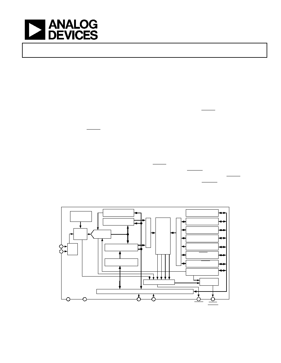
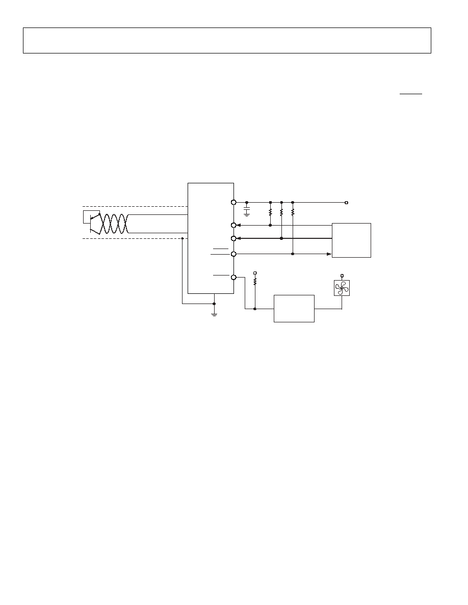
DIGITAL MUX
DIGITAL MUX
SCLK
SDATA
GND
V
DD
6
4
ADDRESS POINTER
REGISTER
LOCAL TEMPERATURE
LOW LIMIT REGISTER
LOCAL TEMPERATURE
HIGH LIMIT REGISTER
REMOTE TEMPERATURE
LOW LIMIT REGISTER
REMOTE TEMPERATURE
HIGH LIMIT REGISTER
LIMIT
COMPARATOR
LOCAL TEMPERATURE
VALUE REGISTER
REMOTE TEMPERATURE
VALUE REGISTER
ADC
ANALOG
MUX
ON-CHIP
TEMPERATURE
SENSOR
RUN/STANDBY
BUSY
REMOTE OFFSET
REGISTER
EXTERNAL DIODE OPEN-CIRCUIT
ADT7461
STATUS REGISTER
SMBus INTERFACE
LOCAL THERM LIMIT
REGISTER
EXTERNAL THERM LIMIT
REGISTER
CONFIGURATION
REGISTER
INTERRUPT
MASKING
7
5
1 8
THERM
ALERT/
THERM2
D+
D
SRC
BLOCK
2
3
CONVERSION RATE
REGISTER
Figure 1. Functional Block Diagram
Information furnished by Analog Devices is believed to be accurate and reliable.
However, no responsibility is assumed by Analog Devices for its use, nor for any
infringements of patents or other rights of third parties that may result from its use.
Specifications subject to change without notice. No license is granted by implication
or otherwise under any patent or patent rights of Analog Devices. Trademarks and
registered trademarks are the property of their respective owners.
One Technology Way, P.O. Box 9106, Norwood, MA 02062-9106, U.S.A.
Tel: 781.329.4700
www.analog.com
Fax: 781.326.8703
© 2003 Analog Devices, Inc. All rights reserved.
Rev. 0

ADT7461
TABLE OF CONTENTS
ADT7461Specifications................................................................. 3
SMBus Timing Specifications ......................................................... 4
Absolute Maximum Ratings............................................................ 5
Thermal Characteristics .............................................................. 5
Pin Configuration and Pin Function Descriptions...................... 6
Typical Performance Characteristics ............................................. 7
Functional Description .................................................................... 9
Series Resistance Cancellation.................................................... 9
Temperature Measurement Method .......................................... 9
Temperature Measurement Results.......................................... 10
Temperature Measurement Range ........................................... 10
Temperature Data Format ......................................................... 10
ADT7461 Registers .................................................................... 11
Serial Bus Interface..................................................................... 14
Addressing the Device ............................................................... 14
Alert Output................................................................................ 16
Low Power Standby Mode......................................................... 16
Sensor Fault Detection .............................................................. 16
The ADT7461 Interrupt System............................................... 17
Application Information ........................................................... 18
Factors Affecting Diode Accuracy ........................................... 18
Thermal Inertia and Self-Heating ............................................ 19
Layout Considerations............................................................... 19
Application Circuit..................................................................... 20
Outline Dimensions ....................................................................... 21
Ordering Guide .......................................................................... 21
REVISION HISTORY
Revision 0: Initial Version
Rev. 0 | Page 2 of 24
ADT7461
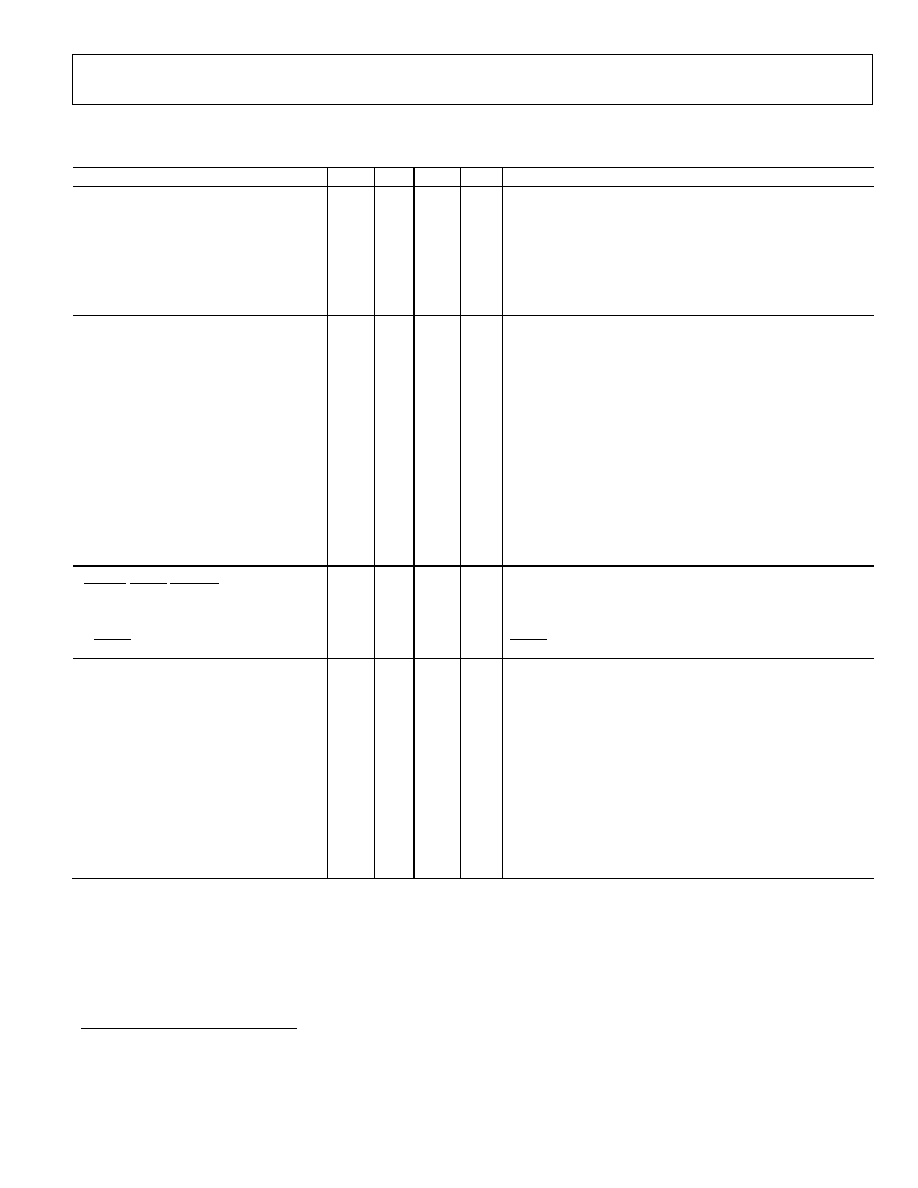
ADT7461SPECIFICATIONS
Table 1. ADT7461 Specifications at T
A
= -40°C to +120°C , V
DD
= 3 V to 5.5 V, unless otherwise noted.
Parameter
Min
Typ
Max
Unit
Test Conditions
POWER SUPPLY
Supply Voltage, V
DD
3.0
3.30
5.5
V
Average Operating Supply Current, I
DD
170
215
µA
0.0625 Conversions/Sec Rate
1
5.5
10
µA
Standby Mode , 40°C T
A
+85°C
5.5
20
µA
Standby Mode, +85°C T
A
+120°C
Undervoltage Lockout Threshold
2.2
2.55
2.8
V
V
DD
Input, Disables ADC, Rising Edge
Power-On-Reset Threshold
1
2.5
V
TEMPERATURE-TO-DIGITAL CONVERTER
Local Sensor Accuracy
±1
±3
°C
-40°C T
A
+100°C, 3 V V
DD
3.6 V
Resolution
1
°C
Remote Diode Sensor Accuracy
±1
°C
+60°C T
A
+100°C, -55°C T
D
2
+150°C, 3 V V
DD
3.6 V
±3
°C
-40°C T
A
+120°C, -55°C T
D
2
+150°C, 3 V V
DD
5.5 V
Resolution
0.25
°C
Remote Sensor Source Current
96
µA
High Level
3
36
µA
Middle
Level
3
6
µA
Low
Level
3
Conversion Time
32.13
114.6
ms
From Stop Bit to Conversion Complete (Both Channels) One-
Shot Mode with Averaging Switched On
3.2
12.56
ms
One-Shot Mode with Averaging Off (i.e., Conversion Rate = 16,
32, or 64 Conversions per Second)
Maximum Series Resistance Cancelled
3
k
Resistance Split Evenly on Both the D+ and D Inputs
OPEN-DRAIN DIGITAL OUTPUTS
(THERM, ALERT/THERM2)
Output Low Voltage, V
OL
0.4
V
I
OUT
= -6.0 mA
3
High Level Output Leakage Current, I
OH
0.1
1
µA
V
OUT
= V
DD
3
ALERT Output Low Sink Current
1
mA
ALERT forced to 0.4 V
SMBus INTERFACE
3, 4
Logic Input High Voltage, V
IH
2.1
V
3 V V
DD
3.6 V
SCLK, SDATA
Logic Input Low Voltage, V
IL
0.8
V
3 V V
DD
3.6 V
SCLK, SDATA
Hysteresis
500
mV
SMBus Output Low Sink Current
6
mA
SDATA Forced to 0.6 V
Logic Input Current, I
IH
, I
IL
-1
+1
µA
SMBus Input Capacitance, SCLK, SDATA
5
pF
SMBus Clock Frequency
400
kHz
SMBus Timeout
5
25
64
ms
User Programmable.
SCLK Falling Edge to SDATA Valid Time
1
µs
Master Clocking in Data
1
See Table 8 for information on other conversion rates.
2
Guaranteed by characterization but not production tested.
3
Guaranteed by design but not production tested.
4
See SMBus Timing Specifications section for more information.
5
Disabled by default. Details on how to enable it are in the SMBus section of this data sheet.
Rev. 0 | Page 3 of 24
ADT7461
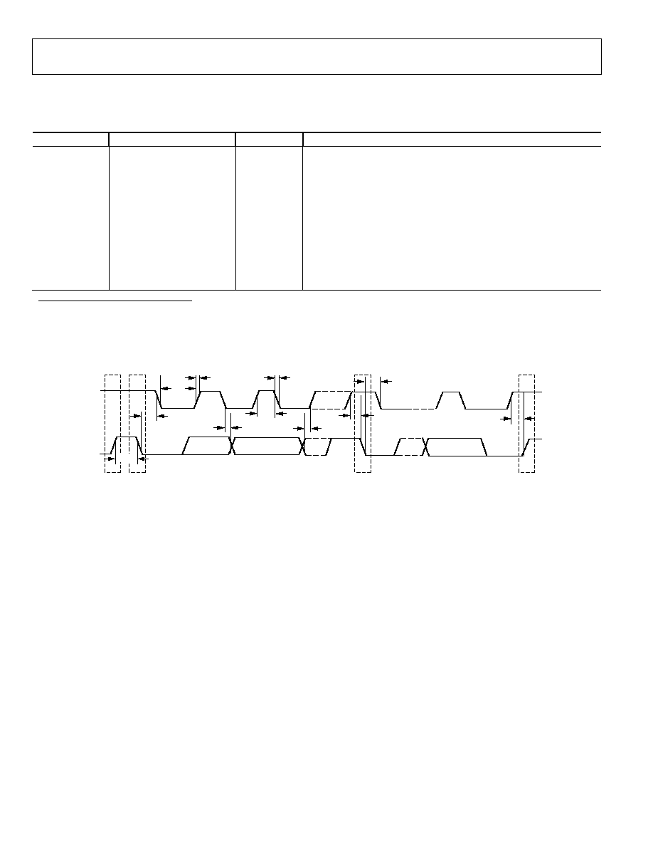
SMBus TIMING SPECIFICATIONS
Table 2. SMBus Timing Specifications
1
Parameter
Limit at T
MIN
, T
MAX
Unit Description
f
SCLK
400
kHz max
t
LOW
4.7
µs min
Clock Low Period, between 10% Points.
t
HIGH
4
µs min
Clock High Period, between 90% Points.
t
R
1
µs max
Clock/Data Rise Time.
t
F
300
ns max
Clock/Data Fall Time.
t
SU; STA
4.7
µs min
Start Condition Setup Time.
t
HD; STA
2
4
µs min
Start Condition Hold Time.
t
SU; DAT
3
250
ns min
Data Setup Time.
t
HD; DAT
300
µs min
Data Hold Time.
t
SU; STO
4
4
µs min
Stop Condition Setup Time.
t
BUF
4.7
µs min
Bus Free Time between Stop and Start Conditions.
1
Guaranteed by design but not production tested.
2
Time from 10% of SDATA to 90% of SCLK.
3
Time for 10% or 90% of SDATA to 10% of SCLK.
4
Time for 90% of SCLK to 10% of SDATA.
04110-0-001
SCLK
SDATA
t
R
t
F
t
LOW
t
HD;DAT
t
HD;STA
t
HIGH
t
SU;DAT
STOP START
STOP
START
t
SU;STA
t
SU;STO
t
HD;STA
t
BUF
Figure 2. Serial Bus Timing
Rev. 0 | Page 4 of 24

ADT7461
ABSOLUTE MAXIMUM RATINGS
Table 3. ADT7461 Absolute Maximum Ratings*
Parameter Rating
Positive Supply Voltage (V
DD
) to GND
-0.3 V, +5.5 V
D+
-0.3 V to V
DD
+ 0.3 V
D- to GND
-0.3 V to +0.6 V
SCLK, SDATA, ALERT
-0.3 V to +5.5 V
THERM
-0.3 V to V
DD
+ 0.3 V
Input Current, SDATA, THERM
-1 mA, +50 mA
Input Current, D-
±1 mA
ESD Rating, All Pins (Human Body Model)
2000 V
Maximum Junction Temperature (T
J
Max)
150°C
Storage Temperature Range
-65°C to +150°C
IR Reflow Peak Temperature
220°C
Lead Temperature (Soldering 10 sec)
300°C
*Stresses above those listed under Absolute Maximum Ratings may cause
permanent damage to the device. This is a stress rating only; functional
operation of the device at these or any other conditions above those indi-
cated in the operational section of this specification is not implied. Exposure
to absolute maximum rating conditions for extended periods may affect
device reliability.
THERMAL CHARACTERISTICS
8-Lead SOIC Package
JA
= 121°C/W
8-Lead MSOP Package
JA
= 142°C/W
Rev. 0 | Page 5 of 24
ADT7461
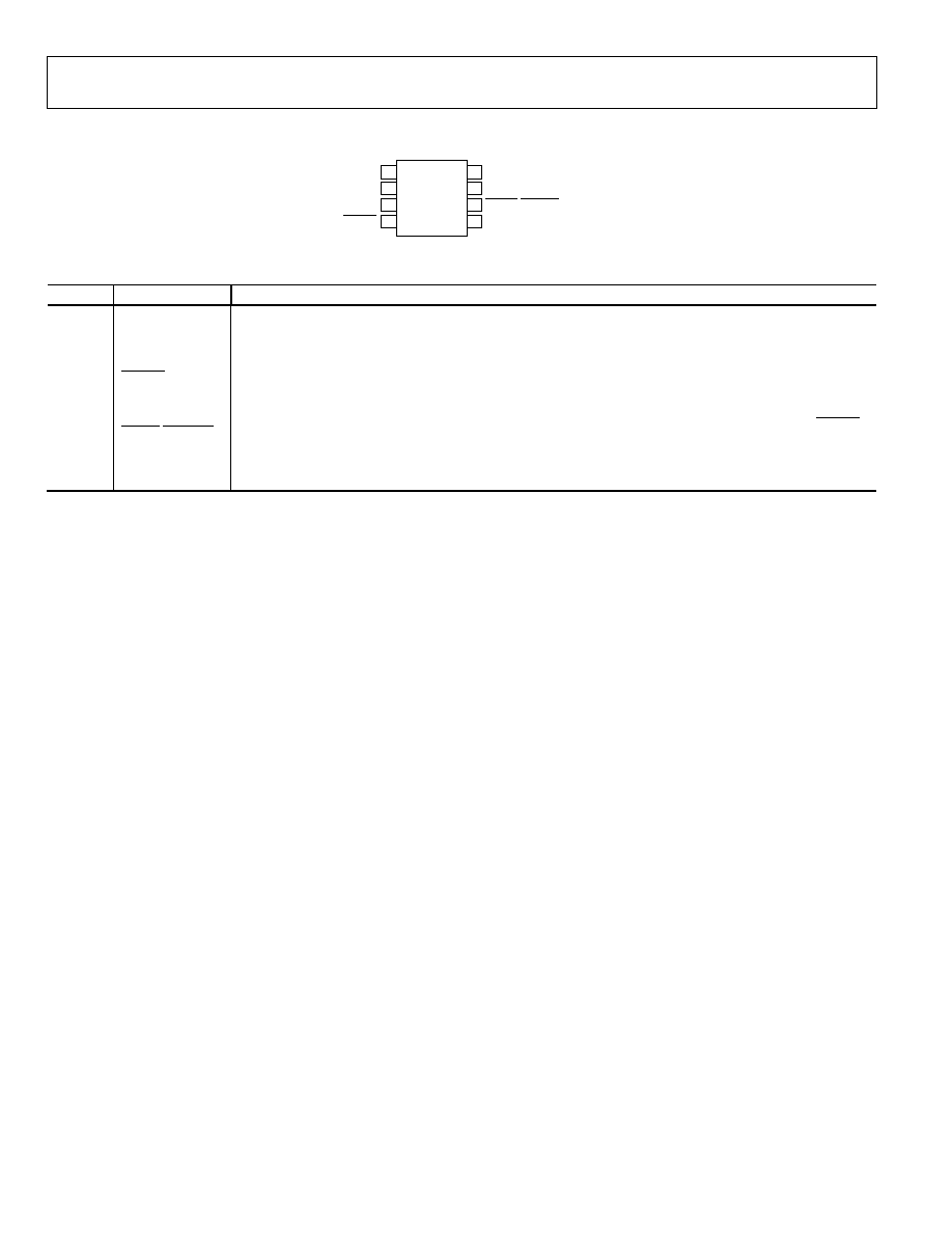
PIN CONFIGURATION AND PIN FUNCTION DESCRIPTIONS
04110-0-013
SCLK
SDATA
ALERT/THERM2
GND
1
V
DD
ADT7461
TOP VIEW
(Not to Scale)
8
2
D+
7
3
D
6
4
THERM
5
Figure 3. Pin Configuration
Table 4. Pin Function Descriptions
Pin No.
Mnemonic
Description
1
V
DD
Positive Supply, 3 V to 5.5 V.
2
D+
Positive Connection to Remote Temperature Sensor.
3
D-
Negative Connection to Remote Temperature Sensor.
4
THERM
Open-Drain Output that can be used to turn a fan on/off or throttle a CPU clock in the event of an
overtemperature condition. Requires pull-up to V
DD
.
5
GND
Supply Ground Connection.
6
ALERT/THERM2
Open-Drain Logic Output used as interrupt or SMBus alert. This may also be configured as a second THERM
output. Requires pull-up resistor.
7
SDATA
Logic Input/Output, SMBus Serial Data. Open-drain output. Requires pull-up resistor.
8
SCLK
Logic Input, SMBus Serial Clock. Requires pull-up resistor.
Rev. 0 | Page 6 of 24
ADT7461
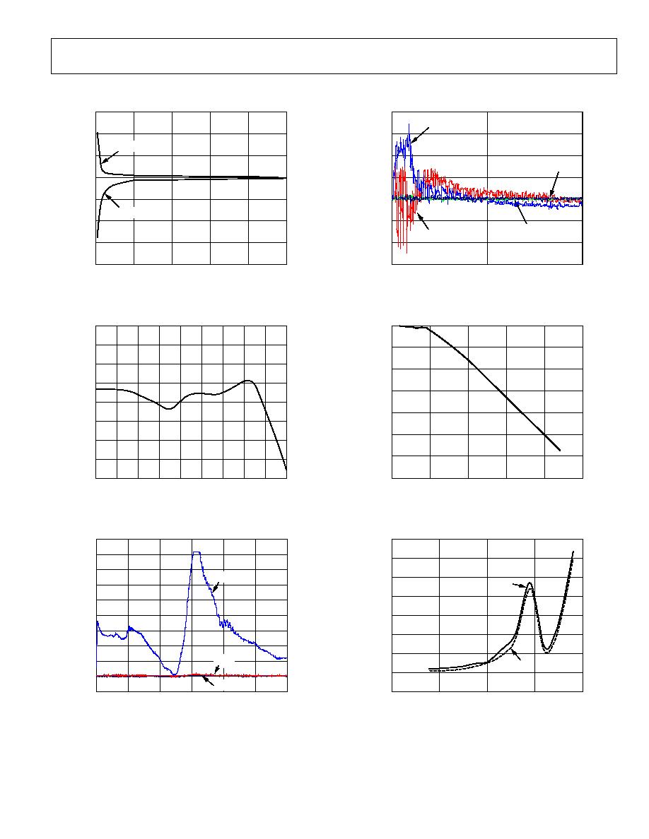
TYPICAL PERFORMANCE CHARACTERISTICS
04110-0-017
60
0
20
40
60
80
LEAKAGE REISITANVE (M
)
100
TE
MP
E
RATURE
E
RROR (
°
C)
80
60
40
20
0
20
40
D+ TO GND
D+ TO V
CC
Figure 4. Temperature Error vs. Leakage Resistance
04110-0-022
3
10
10
30
50
70
90
110
130
150
TEMPERATURE (
°C)
TE
MP
E
RATURE
E
RROR (
°
C)
0.8
0.7
0.6
0.5
0.4
0.3
0.2
0.1
0
Figure 5. Temperature Error vs. Actual Temperature Using 2N3906
04110-0-014
180
160
140
120
100
0
100
200
300
FREQUENCY (MHz)
400
500
600
TE
MP
E
RATURE
E
RROR (
°
C)
80
60
40
20
0
20
60mV
40mV
100mV
Figure 6. Temperature Error vs. Differential Mode Noise Frequency
04110-0-015
20
0
20
FREQUENCY (MHz)
40
TE
MP
E
RATURE
E
RROR (
°
C)
15
10
5
0
5
10
15
250mV EXTERNAL
250mV INTERNAL
100mV EXTERNAL
100mV INTERNAL
Figure 7. Temperature Error vs. Power Supply Noise Frequency
04110-0-018
0
0
5
10
15
20
CAPACITANCE (nF)
25
TE
MP
E
RATURE
E
RROR (
°
C)
70
60
50
40
30
20
10
Figure 8. Temperature Error vs. Capacitance between D+ and D-
04110-0-019
800
0.01
0.1
1
10
3V
5.5V
CONVERSION RATE (Hz)
100
I
DD
(
µ
A)
0
100
200
300
400
500
600
700
Figure 9. Operating Supply Current vs. Conversion Rate
Rev. 0 | Page 7 of 24
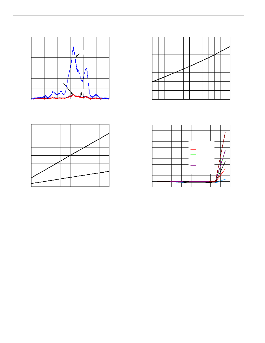
ADT7461
04110-0-016
60
0
100
200
300
400
500
FREQUENCY (MHz)
600
TE
MP
E
RATURE
E
RROR (
°
C)
0
10
20
30
40
50
60mV
100mV
40mV
Figure 10. Temperature Error vs. Common-Mode Noise Frequency
04110-0-020
40
0
100
200
300
3V
5.5V
SCL CLOCK FREQUENCY (kHz)
400
50
150
250
350
I
DD
(
µ
A)
0
5
10
15
20
25
30
35
Figure 11. Standby Supply Current vs. Clock Frequency
04110-0-021
7
3.0 3.2 3.4 3.6 3.8 4.0 4.2 4.4 4.6 4.8 5.0 5.2 5.4
V
DD
(V)
I
DD
(
µ
A)
0
1
2
3
4
5
6
Figure 12. Standby Current vs. Supply Voltage
04110-0-023
0
2
10
200
1k
2k
3k
4k
SERIES RESISTANCE (
)
TE
MP
E
RATURE
E
R
ROR (
°
C)
5
0
5
10
15
20
25
30
35
40
45
50
3.3V T = 30
3.3V T = +25
3.3V T = +120
5.5V T = 30
5.5V T = +25
5.5V T = +120
Figure 13. Temperature Error vs. Series Resistance
Rev. 0 | Page 8 of 24

ADT7461
FUNCTIONAL DESCRIPTION
The ADT7461 is a local and remote temperature sensor and
over/under temperature alarm, with the added ability to
automatically cancel the effect of 3 k (typical) of resistance
in series with the temperature monitoring diode. When the
ADT7461 is operating normally, the on-board ADC operates in
a free-running mode. The analog input multiplexer alternately
selects either the on-chip temperature sensor to measure its
local temperature or the remote temperature sensor. The ADC
digitizes these signals and the results are stored in the local and
remote temperature value registers.
The local and remote measurement results are compared with
the corresponding high, low, and THERM temperature limits,
stored in eight on-chip registers. Out-of-limit comparisons gen-
erate flags that are stored in the status register. A result that
exceeds the high temperature limit, the low temperature limit,
or an external diode fault will cause the ALERT output to assert
low. Exceeding THERM temperature limits causes the THERM
output to assert low. The ALERT output can be reprogrammed
as a second THERM output.
The limit registers can be programmed, and the device con-
trolled and configured, via the serial SMBus. The contents of
any register can also be read back via the SMBus.
Control and configuration functions consist of: switching the
device between normal operation and standby mode, selecting
the temperature measurement scale, masking or enabling the
ALERT output, switching Pin 6 between ALERT and THERM2,
and selecting the conversion rate.
SERIES RESISTANCE CANCELLATION
Parasitic resistance, seen in series with the remote diode, to the
D+ and D- inputs to the ADT7461, is caused by a variety of
factors, including PCB track resistance and track length. This
series resistance appears as a temperature offset in the remote
sensor's temperature measurement. This error typically causes a
0.5°C offset per ohm of parasitic resistance in series with the
remote diode.
The ADT7461 automatically cancels out the effect of this series
resistance on the temperature reading, giving a more accurate
result, without the need for user characterization of this resis-
tance. The ADT7461 is designed to automatically cancel typically
up to 3 k of resistance. By using an advanced temperature
measurement method, this is transparent to the user. This fea-
ture allows resistances to be added to the sensor path to produce
a filter, allowing the part to be used in noisy environments. See
the section on
for more details.
Noise Filtering
Noise Filtering
TEMPERATURE MEASUREMENT METHOD
A simple method of measuring temperature is to exploit the
negative temperature coefficient of a diode, measuring the
base-emitter voltage (V
BE
) of a transistor, operated at constant
current. Unfortunately, this technique requires calibration to
null out the effect of the absolute value of V
BE
, which varies
from device to device.
The technique used in the ADT7461 is to measure the change
in V
BE
when the device is operated at three different currents.
Previous devices have used only two operating currents, but it is
the use of a third current that allows automatic cancellation of
resistances in series with the external temperature sensor.
Figure 14 shows the input signal conditioning used to measure
the output of an external temperature sensor. This figure shows
the external sensor as a substrate transistor, but it could equally
be a discrete transistor. If a discrete transistor is used, the collec-
tor will not be grounded and should be linked to the base. To
prevent ground noise interfering with the measurement, the
more negative terminal of the sensor is not referenced to
ground but is biased above ground by an internal diode at the
D- input. C1 may optionally be added as a noise filter (recom-
mended maximum value 1000 pF). However, a better option in
noisy environments is to add a filter, as described in the section
on
. See the section on
for
more information on C1.
Layout Considerations
To measure V
BE
, the operating current through the sensor is
switched among three related currents. Shown in Figure 14,
N1 × I and N2 × I are different multiples of the current I. The
currents through the temperature diode are switched between I
and N1 × I, giving V
BE1
, and then between I and N2 × I, giving
V
BE2
. The temperature may then be calculated using the two
V
BE
measurements. This method can also be shown to cancel
the effect of any series resistance on the temperature measurement.
The resulting V
BE
waveforms are passed through a 65 kHz
low-pass filter to remove noise and then to a chopper-stabilized
amplifier. This amplifies and rectifies the waveform to produce
a dc voltage proportional to V
BE
. The ADC digitizes this volt-
age and a temperature measurement is produced. To reduce the
effects of noise, digital filtering is performed by averaging the
results of 16 measurement cycles for low conversion rates. At
rates of 16, 32, and 64 conversions/second, no digital averaging
takes place.
Signal conditioning and measurement of the internal tempera-
ture sensor is performed in the same manner.
Rev. 0 | Page 9 of 24
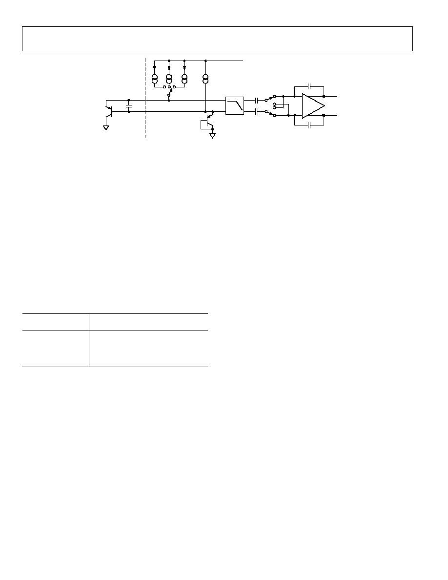
ADT7461
04110-0-002
I
N1
×
I
N2
×
I
I
BIAS
V
DD
V
OUT+
TO ADC
V
OUT
REMOTE
SENSING
TRANSISTOR
*CAPACITOR C1 IS OPTIONAL. IT SHOULD ONLY BE USED IN NOISY ENVIRONMENTS.
D+
D
C1*
BIAS
DIODE
LOW-PASS FILTER
f
C
= 65kHz
Figure 14. Input Signal Conditioning
TEMPERATURE MEASUREMENT RESULTS
The results of the local and remote temperature measurements
are stored in the local and remote temperature value registers
and are compared with limits programmed into the local and
remote high and low limit registers.
The local temperature value is in Register 0×00 and has a
resolution of 1°C. The external temperature value is stored in
two registers, with the upper byte in Register 0×01 and the
lower byte in Register 0×10. Only the two MSBs in the external
temperature low byte are used. This gives the external tempera-
ture measurement a resolution of 0.25°C. T
shows the data
format for the external temperature low byte.
able 5
Table 5. Extended Temperature Resolution (Remote
Temperature Low Byte)
Extended
Resolution
Remote Temperature Low Byte
0.00°C
0 000 0000
0.25°C
0 100 0000
0.50°C
1 000 0000
0.75°C
1 100 0000
When reading the full external temperature value, both the high
and low byte, the two registers should be read in succession.
Reading one register does not lock the other, so both should be
read before the next conversion finishes. In practice, there is
more than enough time to read both registers, as transactions
over the SMBus are significantly faster than a conversion time.
TEMPERATURE MEASUREMENT RANGE
The temperature measurement range for both internal and
external measurements is, by default, 0°C to +127°C. However,
the ADT7461 can be operated using an extended temperature
range. It can measure the full temperature range of an external
diode, from -55°C to +150°C. The user can switch between
these two temperature ranges by setting or clearing Bit 2 in
the configuration register. A valid result is available in the next
measurement cycle after changing the temperature range.
In extended temperature mode, the upper and lower tempera-
ture that can be measured by the ADT7461 is limited by the
remote diode selection. The temperature registers themselves
can have values from -64°C to +191°C. However, most tem-
perature sensing diodes have a maximum temperature range of
-55°C to +150°C.
It should be noted that while both local and remote temperature
measurements can be made while the part is in extended
temperature mode, the ADT7461 itself should not be exposed to
temperatures greater than those specified in the absolute maximum
ratings section. Further, the device is only guaranteed to operate as
specified at ambient temperatures from -40°C to +120°C.
TEMPERATURE DATA FORMAT
The ADT7461 has two temperature data formats. When the
temperature measurement range is from 0°C to +127°C (de-
fault), the temperature data format for both internal and exter-
nal temperature results is binary. When the measurement range
is in extended mode, an offset binary data format is used for
both internal and external results. Temperature values in the
offset binary data format are offset by +64. Examples of tem-
peratures in both data formats are shown in
.
Table 6
Rev. 0 | Page 10 of 24

ADT7461
Table 6. Temperature Data Format (Local and Remote Temperature High Byte)
Temperature
Binary
Offset Binary
1
55°C
0 000 0000
2
0 000 1001
0°C
0 000 0000
0 100 0000
+1°C
0 000 0001
0 100 0001
+10°C
0 000 1010
0 100 1010
+25°C
0 001 1001
0 101 1001
+50°C
0 011 0010
0 111 0010
+75°C
0 100 1011
1 000 1011
+100°C
0 110 0100
1 010 0100
+125°C
0 111 1101
1 011 1101
+127°C
0 111 1111
1 011 1111
+150°C
0 111 1111
3
1 101 0110
1
Offset binary scale temperature values are offset by +64.
2
Binary scale temperature measurement returns 0 for all temperatures < 0°C.
3
Binary scale temperature measurement returns 127 for all temperature > 127°C.
The user may switch between measurement ranges at any time.
Switching the range will also switch the data format. The next
temperature result following the switching will be reported back
to the register in the new format. However, the contents of the
limit registers will not change. It is up to the user to ensure that
when the data format changes, the limit registers are repro-
grammed as necessary. More information on this can be found
in the
section.
Limit Registers
ADT7461 REGISTERS
The ADT7461 contains 22 8-bit registers in total. These regis-
ters are used to store the results of remote and local temperature
measurements and high and low temperature limits and to con-
figure and control the device. A description of these registers
follows, and further details are given in Table 7 through Table 11.
Address Pointer Register
The address pointer register itself does not have, or require, an
address, as the first byte of every write operation is automati-
cally written to this register. The data in this first byte always
contains the address of another register on the ADT7461, which
is stored in the address pointer register. It is to this register
address that the second byte of a write operation is written to or
to which a subsequent read operation is performed.
The power-on default value of the address pointer register is
0×00, so if a read operation is performed immediately after
power-on, without first writing to the address pointer, the value
of the local temperature will be returned, since its register
address is 0×00.
Temperature Value Registers
The ADT7461 has three registers to store the results of local and
remote temperature measurements. These registers can only be
written to by the ADC and can be read by the user over the
SMBus. The local temperature value register is at Address 0×00.
The external temperature value high byte register is at Address
0×01, with the low byte register at Address 0×10. The power-on
default for all three registers is 0×00.
Configuration Register
The configuration register is Address 0×03 at read and Address
0×09 at write. Its power-on default is 0×00. Only four bits of the
configuration register are used. Bits 0, 1, 3, and 4 are reserved
and should not be written to by the user.
Bit 7 of the configuration register is used to mask the ALERT
output. If Bit 7 is 0, the ALERT output is enabled. This is the
power-on default. If Bit 7 is set to 1, the ALERT output is dis-
abled. This only applies if Pin 6 is configured as ALERT. If Pin 6
is configured as THERM2, then the value of Bit 7 has no effect.
If Bit 6 is 0, power-on default, the device is in operating mode
with the ADC converting. If Bit 6 is set to 1, the device is in
standby mode and the ADC does not convert. The SMBus does,
however, remain active in standby mode, so values can be read
from or written to the ADT7461 via the SMBus in this mode.
The ALERT and THERM outputs are also active in standby
mode. Changes made to the registers in standby mode that
affect the THERM or ALERT outputs will cause these signals to
be updated.
Bit 5 determines the configuration of Pin 6 on the ADT7461. If
Bit 5 is 0, (default) then Pin 6 is configured as an ALERT output.
If Bit 5 is 1, then Pin 6 is configured as a THERM2 output. Bit 7,
the ALERT mask bit, is only active when Pin 6 is configured as
an ALERT output. If Pin 6 is setup as a THERM2 output, then
Bit 7 has no effect.
Bit 2 sets the temperature measurement range. If Bit 2 is 0
(default value), the temperature measurement range is set
between 0°C to +127°C. Setting Bit 2 to 1 means that the meas-
urement range is set to the extended temperature range.
Rev. 0 | Page 11 of 24
ADT7461
Table 7. Configuration Register Bit Assignments
Bit
Name
Function
Power-On
Default
7
MASK1
0 = ALERT Enabled
1 = ALERT Masked
0
6
RUN/STOP
0 = Run
1 = Standby
0
5
ALERT/THERM2
0 = ALERT
1 = THERM2
0
4
3
Reserved
0
2
Temperature
Range Select
0 = 0°C to 127°C
1 = Extended
Range
0
1
0
Reserved
0
Conversion Rate Register
The conversion rate register is Address 0×04 at read and
Address 0×0A at write. The lowest four bits of this register are
used to program the conversion rate by dividing the internal
oscillator clock by 1, 2, 4, 8, 16, 32, 64, 128, 256, 512, or 1024 to
give conversion times from 15.5 ms (Code 0×0A) to 16 seconds
(Code 0×00). For example, a conversion rate of 8 conver-
sions/second means that beginning at 125 ms intervals the
device performs a conversion on the internal and the external
temperature channels.
This register can be written to and read back over the SMBus.
The higher four bits of this register are unused and must be set
to 0. The default value of this register is 0×08, giving a rate of 16
conversions per second. Use of slower conversion times greatly
reduces the device power consumption, as shown in
.
Table 8
Table 8. Conversion Rate Register Codes
Code
Conversion/Second
Average Supply
Current µA Typ
at V
DD
= 5.5 V
0×00 0.0625
121.33
0×01 0.125
128.54
0×02 0.25
131.59
0×03 0.5
146.15
0×04 1
169.14
0×05 2
233.12
0×06 4
347.42
0×07 8
638.07
0×08 16
252.44
0×09 32
417.58
0×0A 64
816.87
0×0B to 0×FF
Reserved
Limit Registers
The ADT7461 has eight limit registers: high, low, and THERM
temperature limits for both local and remote temperature
measurements. The remote temperature high and low limits
span two registers each, to contain an upper and lower byte for
each limit. There is also a THERM hysteresis register. All limit
registers can be written to and read back over the SMBus. See
for details of the limit registers' addresses and their
power-on default values.
Table 12
When Pin 6 is configured as an ALERT output, the high limit
registers perform a > comparison while the low limit registers
perform a comparison. For example, if the high limit register
is programmed with 80°C, then measuring 81°C will result in an
out-of-limit condition, setting a flag in the status register. If the
low limit register is programmed with 0°C, measuring 0°C or
lower will result in an out-of-limit condition.
Exceeding either the local or remote THERM limit asserts
THERM low. When Pin 6 is configured as THERM2, exceeding
either the local or remote high limit asserts THERM2 low. A
default hysteresis value of 10°C is provided that applies to both
THERM channels. This hysteresis value may be reprogrammed
to any value after power up (Register Address 0×21).
It is important to remember that the temperature limits data
format is the same as the temperature measurement data
format. So if the temperature measurement uses default binary,
then the temperature limits also use the binary scale. If the
temperature measurement scale is switched, however, the
temperature limits do not switch automatically. The user must
reprogram the limit registers to the desired value in the correct
data format. For example, if the remote low limit is set at 10°C
and the default binary scale is being used, the limit register
value should be 0000 1010b. If the scale is switched to offset
binary, the value in the low temperature limit register should be
reprogrammed to be 0100 1010b.
Status Register
The status register is a read-only register, at Address 0×02. It
contains status information for the ADT7461.
Bit 7 of the status register indicates that the ADC is busy con-
verting when it is high. The other bits in this register flag the
out-of-limit temperature measurements (Bits 63 and Bits 10)
and the remote sensor open circuit (Bit 2).
If Pin 6 is configured as an ALERT output, the following applies. If
the local temperature measurement exceeds its limits, Bit 6 (high
limit) or Bit 5 (low limit) of the status register asserts to flag this
condition. If the remote temperature measurement exceeds its lim-
its, then Bit 4 (high limit) or Bit 3 (low limit) asserts. Bit 2 asserts to
flag an open-circuit condition on the remote sensor. These five flags
are NOR'd together, so if any of them is high, the ALERT interrupt
latch will be set and the ALERT output will go low.
Rev. 0 | Page 12 of 24
ADT7461
Reading the status register will clear the five flags, Bits 62,
provided the error conditions that caused the flags to be set
have gone away. A flag bit can only be reset if the corresponding
value register contains an in-limit measurement or if the sensor
is good.
The ALERT interrupt latch is not reset by reading the status
register. It will be reset when the ALERT output has been
serviced by the master reading the device address, provided the
error condition has gone away and the status register flag bits
have been reset.
When Flag 1 and/or Flag 0 are set, the THERM output goes low
to indicate that the temperature measurements are outside the
programmed limits. The THERM output does not need to be
reset, unlike the ALERT output. Once the measurements are
within the limits, the corresponding status register bits are reset
automatically, and the THERM output goes high. The user may
add hysteresis by programming Register 0×21. The THERM
output will be reset only when the temperature falls to limit
valuehysteresis value.
When Pin 6 is configured as THERM2, only the high tempera-
ture limits are relevant. If Flag 6 and/or Flag 4 are set, the
THERM2 output goes low to indicate that the temperature
measurements are outside the programmed limits. Flag 5 and
Flag 3 have no effect on THERM2. The behavior of THERM2 is
otherwise the same as THERM.
Table 9. Status Register Bit Assignments
Bit Name
Function
7
BUSY
1 When ADC Converting
6
LHIGH*
1 When Local High Temperature Limit Tripped
5
LLOW*
1 When Local Low Temperature Limit Tripped
4
RHIGH*
1 When Remote High Temperature Limit Tripped
3
RLOW*
1 When Remote Low Temperature Limit Tripped
2
OPEN*
1 When Remote Sensor Open Circuit
1
RTHRM
1 When Remote THERM Limit Tripped
0
LTHRM
1 When Local THERM Limit Tripped
*These flags stay high until the status register is read, or they are reset by POR.
Offset Register
Offset errors may be introduced into the remote temperature
measurement by clock noise or by the thermal diode being
located away from the hot spot. To achieve the specified accu-
racy on this channel, these offsets must be removed.
The offset value is stored as a 10-bit, twos complement value in
Registers 0×11 (high byte) and 0×12 (low byte, left justified).
Only the upper 2 bits of register 0×12 are used. The MSB of
Register 0×11 is the sign bit. The minimum offset that can be
programmed is -128°C, and the maximum is +127.75°C. The
value in the offset register is added or subtracted to the meas-
ured value of the remote temperature.
The offset register powers up with a default value of 0°C and
will have no effect unless the user writes a different value to it.
Table 10. Sample Offset Register Codes
Offset Value
0×11
0×12
-128°C
1000 0000
00 00 0000
-4°C
1111 1100
00 00 0000
-1°C
1111 1111
00 000000
-0.25°C
1111 1111
10 00 0000
0°C
0000 0000
00 00 0000
+0.25°C
0000 0000
01 00 0000
+1°C
0000 0001
00 00 0000
+4°C
0000 0100
00 00 0000
+127.75°C
0111 1111
11 00 0000
One-Shot Register
The one-shot register is used to initiate a conversion and com-
parison cycle when the ADT7461 is in standby mode, after
which the device returns to standby. Writing to the one-shot
register address (0×0F) causes the ADT7461 to perform a con-
version and comparison on both the internal and the external
temperature channels. This is not a data register as such, and it
is the write operation to Address 0×0F that causes the one-shot
conversion. The data written to this address is irrelevant and is
not stored.
Consecutive ALERT Register
The value written to this register determines how many out-of-
limit measurements must occur before an ALERT is generated.
The default value is that one out-of-limit measurement gener-
ates an ALERT. The maximum value that can be chosen is 4.
The purpose of this register is to allow the user to perform
some filtering of the output. This is particularly useful at the
fastest three conversion rates, where no averaging takes place.
This register is at Address 0×22.
Table 11. Consecutive ALERT Register Bit
Register Value
Number of Out-of-Limit
Measurements Required
y××× 000×
1
y××× 001×
2
y××× 011×
3
y××× 111×
4
× = Don't care bit.
y = SMBus timeout bit. Default = 0. See SMBus section for more information.
Rev. 0 | Page 13 of 24
ADT7461
Table 12. List of ADT7461 Registers
Read Address (Hex)
Write Address (Hex)
Name
Power-On Default
Not Applicable
Not Applicable
Address Pointer
Undefined
00
Not Applicable
Local Temperature Value
0000 0000 (0×00)
01
Not Applicable
External Temperature Value High Byte
0000 0000 (0×00)
02
Not Applicable
Status
Undefined
03
09
Configuration
0000 0000 (0×00)
04
0A
Conversion Rate
0000 1000 (0×08)
05
0B
Local Temperature High Limit
0101 0101 (0×55) (85°C)
06
0C
Local Temperature Low Limit
0000 0000 (0×00) (0°C)
07
0D
External Temperature High Limit High Byte
0101 0101 (0×55) (85°C)
08
0E
External Temperature Low Limit High Byte
0000 0000 (0×00) (0°C)
Not Applicable
0F
One-Shot
10
Not Applicable
External Temperature Value Low Byte
0000 0000
11
11
External Temperature Offset High Byte
0000 0000
12
12
External Temperature Offset Low Byte
0000 0000
13
13
External Temperature High Limit Low Byte
0000 0000
14
14
External Temperature Low Limit Low Byte
0000 0000
19
19
External THERM Limit
0110 1100 (0×55) (85°C)
20
20
Local THERM Limit
0101 0101 (0×55) (85°C)
21
21
THERM Hysteresis
0000 1010 (0×0A) (10°C)
22
22
Consecutive ALERT
0000 0001 (0×01)
FE
Not Applicable
Manufacturer ID
0100 0001 (0×41)
FF
Not Applicable
Die Revision Code
0101 0001 (0×51)
*Writing to address 0F causes the ADT7461 to perform a single measurement. It is not a data register as such and it does not matter what data is written to it.
SERIAL BUS INTERFACE
Control of the ADT7461 is carried out via the serial bus. The
ADT7461 is connected to this bus as a slave device, under the
control of a master device.
The ADT7461 has an SMBus timeout feature. When this is en-
abled, the SMBus will timeout after typically 25 ms of no activ-
ity. However, this feature is not enabled by default. Bit 7 of the
consecutive alert register (Address = 0×22) should be set to
enable it.
The ADT7461 supports packet error checking (PEC) and its use
is optional. It is triggered by supplying the extra clock for the
PEC byte. The PEC byte is calculated using CRC-8. The frame
check sequence (FCS) conforms to CRC-8 by the polynomial
( )
1
1
2
8
+
+
+
=
x
x
x
x
C
Consult the SMBus 1.1 specification for more information
(www.smbus.org).
ADDRESSING THE DEVICE
In general, every SMBus device has a 7-bit device address,
except for some devices that have extended, 10-bit addresses.
When the master device sends a device address over the bus, the
slave device with that address will respond. The ADT7461 is
available with one device address, 0×4C (1001 100b).
The serial bus protocol operates as follows:
1. The master initiates data transfer by establishing a START
condition, defined as a high-to-low transition on the serial
data line SDATA, while the serial clock line SCLK remains
high. This indicates that an address/data stream will follow.
All slave peripherals connected to the serial bus respond to
the START condition and shift in the next eight bits, con-
sisting of a 7-bit address (MSB first) plus an R/W bit,
which determines the direction of the data transfer, i.e.,
whether data will be written to or read from the slave
device. The peripheral whose address corresponds to the
transmitted address responds by pulling the data line low
during the low period before the ninth clock pulse, known
as the Acknowledge Bit. All other devices on the bus now
remain idle while the selected device waits for data to be
read from or written to it. If the R/W bit is a 0, the master
will write to the slave device. If the R/W bit is a 1, the mas-
ter will read from the slave device.
2. Data is sent over the serial bus in a sequence of nine clock
pulses, eight bits of data followed by an Acknowledge Bit
from the slave device. Transitions on the data line must
occur during the low period of the clock signal and remain
stable during the high period, since a low-to-high transition
when the clock is high may be interpreted as a STOP signal.
The number of data bytes that can be transmitted over the
Rev. 0 | Page 14 of 24
ADT7461
serial bus in a single read or write operation is limited only
by what the master and slave devices can handle.
3. When all data bytes have been read or written, stop condi-
tions are established. In write mode, the master will pull the
data line high during the tenth clock pulse to assert a STOP
condition. In read mode, the master device will override
the acknowledge bit by pulling the data line high during
the low period before the ninth clock pulse. This is known
as No Acknowledge. The master will then take the data line
low during the low period before the tenth clock pulse,
then high during the tenth clock pulse to assert a STOP
condition.
Any number of bytes of data may be transferred over the serial
bus in one operation, but it is not possible to mix read and write
in one operation because the type of operation is determined at
the beginning and cannot subsequently be changed without
starting a new operation. In the case of the ADT7461, write
operations contain either one or two bytes, while read opera-
tions contain one byte.
To write data to one of the device data registers or to read
data from it, the address pointer register must be set so that the
correct data register is addressed. The first byte of a write opera-
tion always contains a valid address that is stored in the address
pointer register. If data is to be written to the device, the write
operation contains a second data byte that is written to the
register selected by the address pointer register.
This is illustrated in
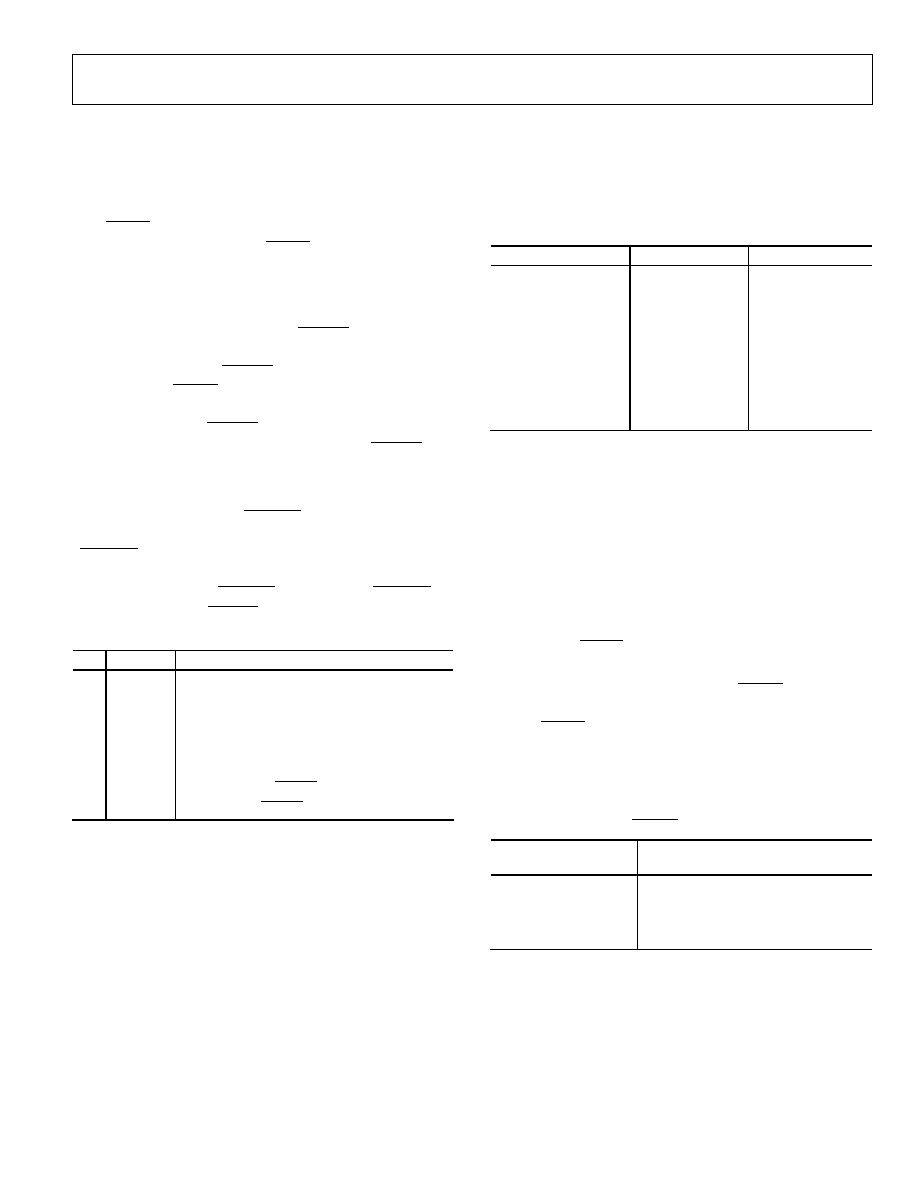
. The device address is sent over
the bus followed by R/W set to 0. This is followed by two data
bytes. The first data byte is the address of the internal data
register to be written to, which is stored in the address pointer
register. The second data byte is the data to be written to the
internal data register.
Figure 15
Figure 15. Writing a Register Address to the Address Pointer Register, then Writing Data to the Selected Register
04110-0-003
A6
1
9
1
A5
A4
A3
A2
A1
A0
R/W
D7
D6
D5
D4
D3
D2
D1
D0
SCLK
SDAT
9
A
START BY
MASTER
ACK. BY
ADT7461
FRAME 1
SERIAL BUS ADDRESS BYTE
FRAME 2
ADDRESS POINTER REGISTER BYTE
FRAME 3
DATA BYTE
SCLK (CONTINUED)
SDATA (CONTINUED)
ACK. BY
ADT7461
ACK. BY
ADT7461
STOP BY
MASTER
9
1
D7
D6
D5
D4
D3
D2
D1
D0
04110-0-004
SCLK
SDATA
START BY
MASTER
ACK. BY
ADT7461
ACK. BY
ADT7461
STOP BY
MASTER
FRAME 1
SERIAL BUS ADDRESS BYTE
FRAME 2
ADDRESS POINTER REGISTER BYTE
1
9
1
A6
A5
A4
A3
A2
A1
A0
R/W
D7
D6
D5
D4
D3
D2
D1
D0
9
Figure 16. Writing to the Address Pointer Register Only
04110-0-005
SCLK
SDATA
START BY
MASTER
ACK. BY
ADT7461
FRAME 1
SERIAL BUS ADDRESS BYTE
FRAME 2
DATA BYTE FROM ADT7461
ACK. BY
ADT7461
STOP BY
MASTER
1
9
1
9
A6
A5
A4
A3
A2
A1
A0
R/W
D7
D6
D5
D4
D3
D2
D1
D0
Figure 17. Reading from a Previously Selected Register
Rev. 0 | Page 15 of 24

ADT7461
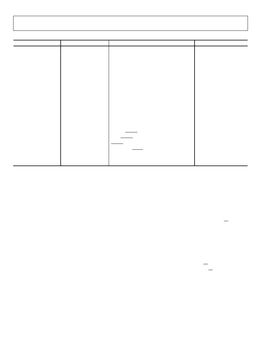
04110-0-006
ALERT RESPONSE
ADDRESS
MASTER SENDS
ARA AND READ
COMMAND
DEVICE SENDS
ITS ADDRESS
RD
START
ACK
DEVICE
ADDRESS
NO
ACK STOP
MASTER
RECEIVES
SMBALERT
When reading data from a register there are two possibilities:
· If the ADT7461's address pointer register value is unknown
or not the desired value, it is first necessary to set it to the
correct value before data can be read from the desired data
register. This is done by performing a write to the
ADT7461 as before, but only the data byte containing the
register read address is sent, as data is not to be written to
the register. This is shown in F
.
A read operation is then performed consisting of the serial
bus address, R/W bit set to 1, followed by the data byte read
from the data register. This is shown in
.
igure 16
igure 16
Figure 17
· If the address pointer register is known to be already at the
desired address, data can be read from the corresponding
data register without first writing to the address pointer
register and the bus transaction shown in F
can be
omitted.
Notes
1. Although it is possible to read a data byte from a data
register without first writing to the address pointer register,
if the address pointer register is already at the correct value,
it is not possible to write data to a register without writing
to the address pointer register because the first data byte of
a write is always written to the address pointer register.
2. Do not forget that some of the ADT7461 registers have
different addresses for read and write operations. The
write address of a register must be written to the address
pointer if data is to be written to that register, but it may
not be possible to read data from that address. The read
address of a register must be written to the address pointer
before data can be read from that register.
ALERT OUTPUT
This is applicable when Pin 6 is configured as an ALERT
output. The ALERT output goes low whenever an out-of-limit
measurement is detected, or if the remote temperature sensor is
open circuit. It is an open-drain output and requires a pull-up to
V
DD
. Several ALERT outputs can be wire-ORed together, so that
the common line will go low if one or more of the ALERT
outputs goes low.
The ALERT output can be used as an interrupt signal to a
processor, or it may be used as an SMBALERT. Slave devices on
the SMBus cannot normally signal to the bus master that they
want to talk, but the SMBALERT function allows them to do so.
One or more ALERT outputs can be connected to a
common SMBALERT line connected to the master. When
the SMBALERT line is pulled low by one of the devices, the
following procedure occurs as illustrated in F
.
igure 18
Figure 18. Use of SMBALERT
1. SMBALERT is pulled low.
2. Master initiates a read operation and sends the alert
response address (ARA = 0001 100). This is a general call
address that must not be used as a specific device address.
3. The device whose ALERT output is low responds to the
alert response address and the master reads its device
address. As the device address is seven bits, an LSB of 1 is
added. The address of the device is now known and it can
be interrogated in the usual way.
4. If more than one device's ALERT output is low, the one
with the lowest device address will have priority, in accor-
dance with normal SMBus arbitration.
5. Once the ADT7461 has responded to the alert response
address, it will reset its ALERT output, provided that the
error condition that caused the ALERT no longer exists. If
the SMBALERT line remains low, the master will send the
ARA again, and so on until all devices whose ALERT
outputs were low have responded.
LOW POWER STANDBY MODE
The ADT7461 can be put into low power standby mode by
setting Bit 6 of the configuration register. When Bit 6 is low, the
ADT7461 operates normally. When Bit 6 is high, the ADC is
inhibited, and any conversion in progress is terminated without
writing the result to the corresponding value register.
The SMBus is still enabled. Power consumption in the standby
mode is reduced to less than 10 µA if there is no SMBus activity
or 100 µA if there are clock and data signals on the bus.
When the device is in standby mode, it is still possible to initiate
a one-shot conversion of both channels by writing to the one-
shot register (Address 0×0F), after which the device will return
to standby. It does not matter what is written to the one-shot
register, all data written to it is ignored. It is also possible to
write new values to the limit register while in standby mode. If
the values stored in the temperature value registers are now
outside the new limits, an ALERT is generated, even though the
ADT7461 is still in standby.
SENSOR FAULT DETECTION
The ADT7461 has sensor fault detection circuitry internally at
its D+ input. This circuit can detect situations where an external
remote diode is not connected, or is incorrectly connected, to
Rev. 0 | Page 16 of 24
ADT7461
the ADT7461. A simple voltage comparator trips if the voltage
at D+ exceeds V
DD
-1 V (typical), signifying an open circuit
between D+ and D-. The output of this comparator is checked
when a conversion is initiated. Bit 2 of the status register (OPEN
flag) is set if a fault is detected. If the ALERT pin is enabled,
setting this flag will cause ALERT to assert low.
If the user does not wish to use an external sensor with the
ADT7461, then in order to prevent the OPEN flag being set
continuously, the user should tie the D+ and D- inputs of the
ADT7461 together.
Most temperature sensing diodes have an operating temperature
range of -55°C to +150°C. Above 150°C, they lose their semicon-
ductor characteristics and approximate conductors instead. This
results in a diode short, setting the OPEN flag. The external diode
in this case will no longer give an accurate temperature meas-
urement. A read of the temperature result register will give the
last good temperature measurement. The user should be aware
that, while the diode fault is triggered, the temperature measure-
ment on the external channel may not be accurate.
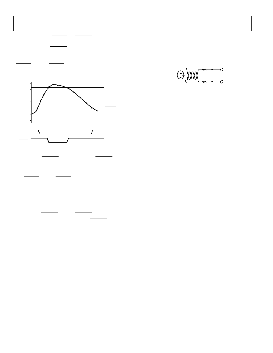
THE ADT7461 INTERRUPT SYSTEM
The ADT7461 has two interrupt outputs, ALERT and THERM.
Both have different functions and behavior. ALERT is maskable
and responds to violations of software-programmed tempera-
ture limits or an open-circuit fault on the external diode.
THERM is intended as a fail-safe interrupt output that cannot
be masked.
If the external or local temperature exceeds the programmed
high temperature limits, or equals or exceeds the low tempera-
ture limits, the ALERT output is asserted low. An open-circuit
fault on the external diode also causes ALERT to assert. ALERT
is reset when serviced by a master reading its device address,
provided the error condition has gone away, and the status
register has been reset.
The THERM output asserts low if the external or local tempera-
ture exceeds the programmed THERM limits. The THERM
temperature limits should normally be equal to or greater than
the high temperature limits. THERM is reset automatically
when the temperature falls back within the THERM limit. The
external THERM limit is set by default to 85°C, as is the local
THERM limit. A hysteresis value can be programmed, in which
case, THERM will reset when the temperature falls to the limit
value minus the hysteresis value. This applies to both local and
remote measurement channels. The power-on hysteresis default
value is 10°C, but this may be reprogrammed to any value after
power-up.
The hysteresis loop on the THERM outputs is useful when
THERM is used for on/off control of a fan. The user's system
can be set up so that when THERM asserts a fan can be
switched on to cool the system. When THERM goes high again,
the fan can be switched off. Programming a hysteresis value
protects from fan jitter, where the temperature hovers around
the THERM limit, and the fan is constantly being switched.
Table 13. THERM Hysteresis
THERM Hysteresis
Binary Representation
0°C
0 000 0000
1°C
0 000 0001
10°C
0 000 1010
shows how the THERM and ALERT outputs operate.
A user may wish to use the ALERT output as a SMBALERT
to signal to the host via the SMBus that the temperature has
risen. The user could use the THERM output to turn on a fan to
cool the system, if the temperature continues to increase. This
method would ensure that there is a fail-safe mechanism to cool
the system, without the need for host intervention.
Figure 19
Figure 19. Operation of the ALERT and THERM Interrupts
Figure 19
04110-
0-
007
1
3
2
4
THERM LIMIT
HIGH TEMP LIMIT
THERM LIMIT-HYSTERESIS
RESET BY MASTER
ALERT
THERM
100
°C
TEMPERATURE
90
°C
80
°C
70
°C
60
°C
50
°C
40
°C
1. If the measured temperature exceeds the high temperature
limit, the ALERT output will assert low.
2. If the temperature continues to increase and exceeds the
THERM limit, the THERM output asserts low. This can be
used to throttle the CPU clock or switch on a fan.
3. The THERM output deasserts (goes high) when the
temperature falls to THERM limit minus hysteresis. In
, the default hysteresis value of 10°C is shown.
4. The ALERT output deasserts only when the temperature
has fallen below the high temperature limit, and the master
has read the device address and cleared the status register.
Pin 6 on the ADT7461 can be configured as either an ALERT
output or as an additional THERM output. THERM2 will assert
low when the temperature exceeds the programmed local
and/or remote high temperature limits. It is reset in the same
manner as THERM, and it is not maskable. The programmed
hysteresis value applies to THERM2 also.
Rev. 0 | Page 17 of 24
ADT7461
Figure 20
Figure 20. Operation of the THERM and THERM2 Interrupts
Figure 20
shows how THERM and THERM2 might operate
together to implement two methods of cooling the system.
In this example, the THERM2 limits are set lower than the
THERM limits. The THERM2 output could be used to turn
on a fan. If the temperature continues to rise and exceeds the
THERM limits, the THERM output could provide additional
cooling by throttling the CPU.
THERM2 LIMIT
THERM LIMIT
04110-0-008
THERM2
1
3
2
4
TEMPERATURE
THERM
90
°C
80
°C
70
°C
60
°C
50
°C
40
°C
30
°C
1. When the THERM2 limit is exceeded, the THERM2 signal
asserts low.
2. If the temperature continues to increase and exceeds the
THERM limit, the THERM output asserts low.
3. The THERM output deasserts (goes high) when the
temperature falls to THERM limit minus hysteresis. In
, there is no hysteresis value shown.
4. As the system cools further, and the temperature falls
below the THERM2 limit, the THERM2 signal resets.
Again, no hysteresis value is shown for THERM2.
The temperature measurement could be either the local or the
external temperature measurement.
APPLICATION INFORMATION
Noise Filtering
For temperature sensors operating in noisy environments, previ-
ous practice was to place a capacitor across the D+ and D- pins
to help combat the effects of noise. However, large capacitances
affect the accuracy of the temperature measurement, leading to a
recommended maximum capacitor value of 1000 pF. While this
capacitor will reduce the noise, it will not eliminate it, making it
difficult to use the sensor in a very noisy environment.
The ADT7461 has a major advantage over other devices when it
comes to eliminating the effects of noise on the external sensor.
The series resistance cancellation feature allows a filter to be
constructed between the external temperature sensor and the
part. The effect of any filter resistance seen in series with the remote
sensor is automatically cancelled from the temperature result.
The construction of a filter allows the ADT7461 and the remote
temperature sensor to operate in noisy environments. F
shows a low-pass R-C-R filter, with the following values: R =
100 and C = 1 nF. This filtering reduces both common-mode
noise and differential noise.
igure 21
Figure 21. Filter Between Remote Sensor and ADT7461
04110-0-009
D+
1nF
100
REMOTE
TEMPERATURE
SENSOR
D
100
FACTORS AFFECTING DIODE ACCURACY
Remote Sensing Diode
The ADT7461 is designed to work with substrate transistors
built into processors or with discrete transistors. Substrate
transistors will generally be PNP types with the collector
connected to the substrate. Discrete types can be either PNP or
NPN transistor connected as a diode (base shorted to collector).
If an NPN transistor is used, the collector and base are
connected to D+ and the emitter to D-. If a PNP transistor is
used, the collector and base are connected to D- and the
emitter to D+.
To reduce the error due to variations in both substrate and
discrete transistors, a number of factors should be taken into
consideration:
· The ideality factor, n
f
, of the transistor is a measure of the
deviation of the thermal diode from ideal behavior. The
ADT7461 is trimmed for an n
f
value of 1.008. The follow-
ing equation may be used to calculate the error introduced
at a temperature T (°C), when using a transistor whose n
f
does not equal 1.008. Consult the processor data sheet for
the n
f
values.
(
)
(
)
T
Kelvin
n
T
f
+
×
=
15
.
273
008
.
1
/
008
.
1
To factor this in, the user can write the T value to the
offset register. It will then be automatically added to or
subtracted from the temperature measurement by the
ADT7461.
· Some CPU manufacturers specify the high and low current
levels of the substrate transistors. The high current level of
the ADT7461, I
HIGH
, is 96 µA and the low level current, I
LOW
,
is 6 µA. If the ADT7461 current levels do not match the
current levels specified by the CPU manufacturer, it may
become necessary to remove an offset. The CPUs data
sheet will advise whether this offset needs to be removed
and how to calculate it. This offset may be programmed to
the offset register. It is important to note that if more than
one offset must be considered, the algebraic sum of these
offsets must be programmed to the offset register.
Rev. 0 | Page 18 of 24

ADT7461
If a discrete transistor is being used with the ADT7461, the best
accuracy will be obtained by choosing devices according to the
following criteria:
· Base-emitter voltage greater than 0.25 V at 6 µA, at the
highest operating temperature.
· Base-emitter voltage less than 0.95 V at 100 µA, at the
lowest operating temperature.
· Base resistance less than 100 .
· Small variation in h
FE
(say 50 to 150) that indicates tight
control of V
BE
characteristics.
Transistors, such as 2N3904, 2N3906, or equivalents in SOT-23
packages, are suitable devices to use.
THERMAL INERTIA AND SELF-HEATING
Accuracy depends on the temperature of the remote sensing
diode and/or the internal temperature sensor being at the same
temperature as that being measured. A number of factors can
affect this. Ideally, the sensor should be in good thermal contact
with the part of the system being measured. If it is not, the
thermal inertia caused by the sensor's mass will cause a lag in
the response of the sensor to a temperature change. In the case
of the remote sensor, this should not be a problem, since it will
either be a substrate transistor in the processor or can be a small
package device, such as SOT-23, placed in close proximity to it.
The on-chip sensor, however, will often be remote from the
processor and will only be monitoring the general ambient
temperature around the package. The thermal time constant of
the SOIC-8 package in still air is about 140 seconds, and if the
ambient air temperature quickly changed by 100 degrees, it
would take about 12 minutes (5 time constants) for the junction
temperature of the ADT7461 to settle within 1 degree of this. In
practice, the ADT7461 package will be in electrical, and hence
thermal, contact with a PCB and may also be in a forced airflow.
How accurately the temperature of the board and/or the forced
airflow reflects the temperature to be measured will also affect
the accuracy. Self-heating due to the power dissipated in the
ADT7461 or the remote sensor causes the chip temperature of
the device or remote sensor to rise above ambient. However, the
current forced through the remote sensor is so small that self-
heating is negligible. In the case of the ADT7461, the worst-case
condition occurs when the device is converting at 64 conver-
sions per second while sinking the maximum current of 1 mA
at the ALERT and THERM output. In this case, the total power
dissipation in the device is about 4.5 mW. The thermal resis-
tance,
JA
, of the SOIC-8 package is about 121°C/W.
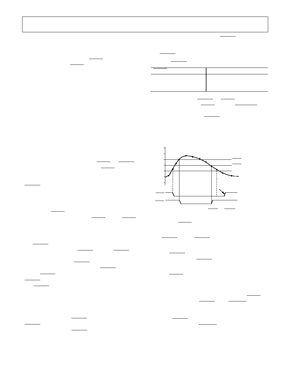
LAYOUT CONSIDERATIONS
Digital boards can be electrically noisy environments, and the
ADT7461 is measuring very small voltages from the remote
sensor, so care must be taken to minimize noise induced at the
sensor inputs. The following precautions should be taken:
· Place the ADT7461 as close as possible to the remote sens-
ing diode. Provided that the worst noise sources, i.e., clock
generators, data/address buses, and CRTs, are avoided, this
distance can be 4 inches to 8 inches.
· Route the D+ and D tracks close together, in parallel,
with grounded guard tracks on each side. To minimize
inductance and reduce noise pick-up, a 5 mil track width
and spacing is recommended. Provide a ground plane
under the tracks if possible.
04110-
0-
010
5MIL
5MIL
5MIL
5MIL
5MIL
5MIL
5MIL
GND
D+
D
GND
Figure 22. Typical Arrangement of Signal Tracks
· Try to minimize the number of copper/solder joints
that can cause thermocouple effects. Where copper/solder
joints are used, make sure that they are in both the D+ and
D- path and at the same temperature.
Thermocouple effects should not be a major problem as
1°C corresponds to about 200 mV, and thermocouple
voltages are about 3 mV/°C of temperature difference.
Unless there are two thermocouples with a big temperature
differential between them, thermocouple voltages should
be much less than 200 mV.
· Place a 0.1 µF bypass capacitor close to the V
DD
pin. In
extremely noisy environments, an input filter capacitor
may be placed across D+ and D- close to the ADT7461.
This capacitance can effect the temperature measurement,
so care must be taken to ensure that any capacitance seen
at D+ and D- is a maximum of 1,000 pF. This maximum
value includes the filter capacitance, plus any cable or stray
capacitance between the pins and the sensor diode.
· If the distance to the remote sensor is more than 8 inches,
the use of twisted pair cable is recommended. This will
work up to about 6 feet to 12 feet.
Rev. 0 | Page 19 of 24
ADT7461
· For really long distances (up to 100 feet), use shielded
twisted pair, such as Belden No. 8451 microphone cable.
Connect the twisted pair to D+ and D- and the shield to
GND close to the ADT7461. Leave the remote end of the
shield unconnected to avoid ground loops.
Because the measurement technique uses switched current
sources, excessive cable or filter capacitance can affect the
measurement. When using long cables, the filter capacitance
may be reduced or removed.
APPLICATION CIRCUIT
Figure 23
Figure 23. Typical Application Circuit
shows a typical application circuit for the ADT7461,
using a discrete sensor transistor connected via a shielded,
twisted pair cable. The pull-ups on SCLK, SDATA, and ALERT
are required only if they are not already provided elsewhere in
the system.
The SCLK and SDATA pins of the ADT7461 can be interfaced
directly to the SMBus of an I/O controller, such as the Intel 820
chipset.
04110-0-011
SHIELD
2N3906
OR
CPU THERMAL
DIODE
ALERT/
THERM2
GND
THERM
D+
D
ADT7461
SCLK
SDATA
V
DD
V
DD
3V TO 3.6V
TYP 10k
TYP 10k
0.1
µF
FAN
CONTROL
CIRCUIT
FAN
ENABLE
SMBUS
CONTROLLER
5V OR 12V
Rev. 0 | Page 20 of 24
ADT7461
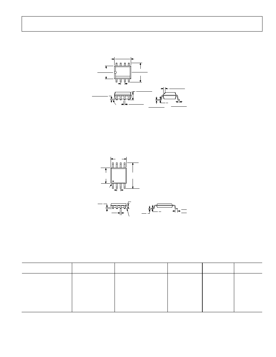
OUTLINE DIMENSIONS
0.25 (0.0098)
0.17 (0.0067)
1.27 (0.0500)
0.40 (0.0157)
0.50 (0.0196)
0.25 (0.0099)
× 45°
8°
0°
1.75 (0.0688)
1.35 (0.0532)
SEATING
PLANE
0.25 (0.0098)
0.10 (0.0040)
4
1
8
5
5.00 (0.1968)
4.80 (0.1890)
4.00 (0.1574)
3.80 (0.1497)
1.27 (0.0500)
BSC
6.20 (0.2440)
5.80 (0.2284)
0.51 (0.0201)
0.31 (0.0122)
COPLANARITY
0.10
CONTROLLING DIMENSIONS ARE IN MILLIMETERS; INCH DIMENSIONS
(IN PARENTHESES) ARE ROUNDED-OFF MILLIMETER EQUIVALENTS FOR
REFERENCE ONLY AND ARE NOT APPROPRIATE FOR USE IN DESIGN
COMPLIANT TO JEDEC STANDARDS MS-012AA
Figure 24. 8-Lead Standard Small Outline Package
[SOIC] (R-8)
Dimensions shown in millimeters and (inches)
0.80
0.60
0.40
8°
0°
4
8
5
4.90
BSC
PIN 1
0.65 BSC
3.00
BSC
SEATING
PLANE
0.15
0.00
0.38
0.22
1.10 MAX
3.00
BSC
COPLANARITY
0.10
0.23
0.08
COMPLIANT TO JEDEC STANDARDS MO-187AA
Figure 25. 8-Lead Micro Small Outline Package
[MSOP] (RM-8)
Dimensions shown in millimeters
ORDERING GUIDE
Model
Operating
Temperature Range
Package Description
Package Option
Branding
Information
SMBus
Address
ADT7461AR
-40°C to +125°C
8-Lead SOIC Package
R-8
ADT7461AR
4C
ADT7461AR-REEL
-40°C to +125°C
8-Lead SOIC Package
R-8
ADT7461AR
4C
ADT7461AR-REEL7
-40°C to +125°C
8-Lead SOIC Package
R-8
ADT7461AR
4C
ADT7461ARM
-40°C to +125°C
8-Lead MSOP Package
RM-8
T1B
4C
ADT7461ARM-REEL
-40°C to +125°C
8-Lead MSOP Package
RM-8
T1B
4C
ADT7461ARM-REEL7
-40°C to +125°C
8-Lead MSOP Package
RM-8
T1B
4C
EVAL-ADT7461EB
ADT7461 Evaluation Board
Rev. 0 | Page 21 of 24

ADT7461
NOTES
Rev. 0 | Page 22 of 24

ADT7461
NOTES
Rev. 0 | Page 23 of 24

ADT7461
Rev. 0 | Page 24 of 24
NOTES
© 2003 Analog Devices, Inc. All rights reserved. Trademarks and
regis-
tered trademarks are the property of their respective owners.
C04110-0-10/03(0)
Document Outline