 | ÐлекÑÑоннÑй компоненÑ: ADV473K50 | СкаÑаÑÑ:  PDF PDF  ZIP ZIP |
ADV473 CMOS 135 MHz True-Color Graphics Triple 8-Bit Video RAM-DAC
REV. A
Information furnished by Analog Devices is believed to be accurate and
reliable. However, no responsibility is assumed by Analog Devices for its
use, nor for any infringements of patents or other rights of third parties
which may result from its use. No license is granted by implication or
otherwise under any patent or patent rights of Analog Devices.
a
CMOS 135 MHz True-Color Graphics
Triple 8-Bit Video RAM-DAC
ADV473
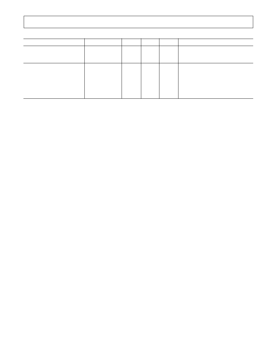
MODES
24-Bit True Color
8-Bit Pseudo Color
15-Bit True Color
8-Bit True Color
SPEED GRADES
135 MHz, 110 MHz
80 MHz, 66 MHz
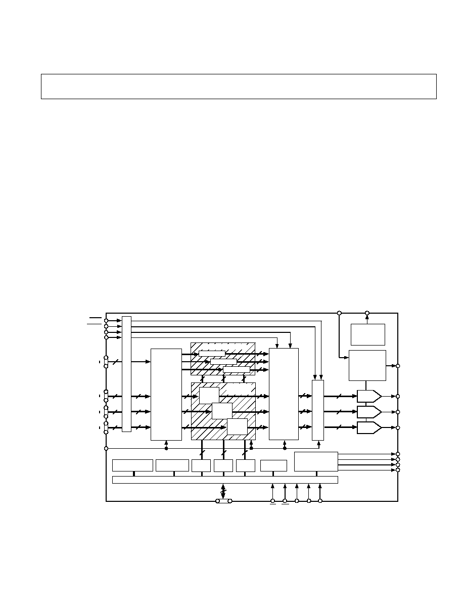
GENERAL DESCRIPTION
The ADV473 is a complete analog output, Video RAM-DAC
on a single CMOS monolithic chip. The part is specifically
designed for true-color computer graphics systems.
The ADV473 integrates a number of graphic functions onto one
device allowing 24-bit direct true-color operation at the maxi-
mum screen update rate of 135 MHz. It can also be used in
other modes, including 15-bit true color and 8-bit pseudo or in-
dexed color. The ADV473 is fully PS/2 and VGA register level
compatible. It is also capable of implementing IBM's XGA
standard.
(Continued on page 4)
FEATURES
ADV478/ADV471 (ADV
®
) Register Level Compatible
IBM PS/2,* VGA*/XGA* Compatible
135 MHz Pipelined Operation
Triple 8-Bit D/A Converters
Triple 256 8 (256 24) Color Palette RAM
Three 15 8 Overlay Registers
On-Board Voltage Reference
RS-343A/RS-170 Compatible Analog Outputs
TTL Compatible Digital Inputs and Outputs
Sync on All Three Channels
Programmable Pedestal (0 or 7.5 IRE)
Standard MPU l/O Interface
+5 V CMOS Monolithic Construction
68-Pin PLCC Package
APPLICATIONS
High Resolution Color Graphics
True-Color Visualization
CAE/CAD/CAM
Image Processing
Desktop Publishing
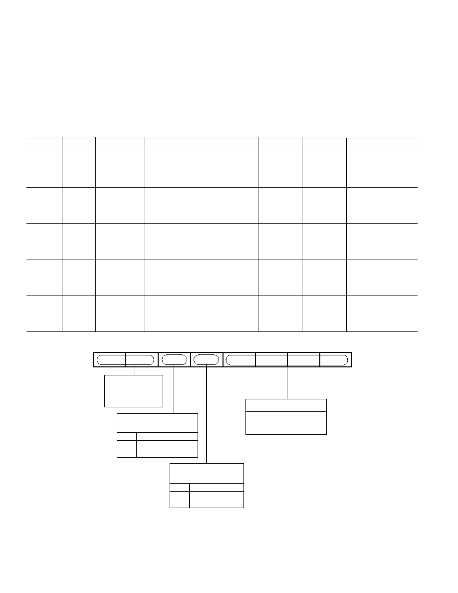
FUNCTIONAL BLOCK DIAGRAM
SWITCHING
MATRIX &
PIXEL
MASK
D
A
C
P
O
R
T
P
I
X
E
L
P
O
R
T
MODE CONTROL
REGISTERS
PIXEL MASK
REGISTERS
RED
REG
GREEN
REG
BLUE
REG
ADDRESS
REG
D0D7
V
REFIN
SYNC
BLANK
RED
GREEN
BLUE
8
COLOR
PALETTE/
OVERLAY
PALETTE
SWITCHER
CLOCK
ADV473
RS0 RS1
RS2
RD
WR
S0
S1
OL0
OL3
R0
R7
G0
G7
B0
B7
V
REFOUT
OPA
IOR
IOB
CR0
CR1
CR2
CR3
MPU PORT
MPU & PIXEL
PORT
CONTROL LOGIC
OVERLAYS
4
IOG
8
8
8
VOLTAGE
REFERENCE
GENERATOR
VOLTAGE
REFERENCE
CONTROL
CIRCUIT
8
8
8
8
8
8
8
8
8
8
8
8
8
8
8
8
8
8
8
8
8
PALETTE
COLOR
RED
256 x 8
RAM
GREEN
256 x 8
RAM
BLUE
256 x 8
RAM
OVERLAY PALETTE
15 x 8 RAM
15 x 8 RAM
15 x 8 RAM
8
8
8
GREEN
DAC
BLUE
DAC
RED
DAC
ADV is a registered trademark of Analog Devices Inc.
*Personal System/2 and VGA are trademarks of International Business Machines Corp.
One Technology Way, P.O. Box 9106, Norwood, MA 02062-9106, U.S.A.
Tel: 617/329-4700
Fax: 617/326-8703

REV. A
2
ADV473SPECIFICATIONS
(V
AA
1
= 5 V; V
REF
= 1.235 V; R
L
= 37.5
, C
L
= 10 pF; R
SET
= 140
.
All specifications T
MIN
to T
MAX
2
unless otherwise noted.)
Parameter
All Versions
Units
Test Conditions/Comments
STATIC PERFORMANCE
Resolution (Each DAC)
8
Bits
Accuracy (Each DAC)
Integral Nonlinearity
±
1
LSB max
Differential Nonlinearity
±
1
LSB max
Guaranteed Monotonic
Gray Scale Error
±
5
% Gray Scale
External Reference
±
10
% Gray Scale
Internal Reference
Coding
Binary
DIGITAL INPUTS
Input High Voltage, V
INH
2
V min
Input Low Voltage, V
INL
0.8
V max
Input Current, I
IN
±
1
µ
A max
V
IN
= 0.4 V or 2.4 V
Input Capacitance, C
IN
7
pF max
f = 1 MHz, V
IN
= 2.4 V
DIGITAL OUTPUTS
Output High Voltage, V
OH
2.4
V min
I
SOURCE
= 400
µ
A
Output Low Voltage, V
OL
0.4
V max
I
SINK
= 3.2 mA
Floating-State Leakage Current
50
µ
A max
Floating-State Leakage Capacitance
7
pF max
ANALOG OUTPUTS
Gray Scale Current Range
20
mA max
Output Current
White Level Relative to Black
16.74
mA min
Typically 17.62 mA
18.50
mA max
Black Level Relative to Blank
0.95
mA min
Typically 1.44 mA
(Pedestal = 7.5 IRE)
1.90
mA max
Black Level Relative to Blank
0
µ
A min
Typically 5
µ
A
(Pedestal = 0 IRE)
50
µ
A max
Blank Level
6.29
mA min
Typically 7.62 mA
8.96
mA max
Sync Level
0
µ
A min
Typically 5
µ
A
50
µ
A max
LSB Size
69.1
µ
A typ
DAC-to-DAC Matching
2
% max
Typically 1%
Output Compliance, V
OC
0
V min
+1.5
V max
Output Capacitance, C
OUT
30
pF max
f = 1 MHz, I
OUT
= 0 mA
Output Impedance, R
OUT
10
k
typ
VOLTAGE REFERENCE
Internal Voltage Reference (V
REFOUT
)
1.08/1.32
V min/V max
Typically 1.235 V
External Voltage Reference Range
1.14/1.26
V min/V max
Typically 1.235 V
Input Current, I
VREF
(Internal Reference)
100
µ
A typ
Input Current (External Reference)
10
µ
A typ
POWER SUPPLY
Supply Voltage, V
AA
4.75/5.25
V min/V max
Supply Current, I
AA
3
400
mA max
135 MHz Parts
300
mA max
110 MHz Parts
250
mA max
80 MHz Parts
200
mA max
66 MHz Parts
DYNAMIC PERFORMANCE
Clock and Data Feedthrough
4, 5
30
dB typ
Glitch Impulse
4, 5
75
pV secs typ
DAC-to-DAC Crosstalk
6
23
dB typ
NOTES
1
V
AA
= 5 V
±
5%
2
Temperature range (T
MIN
to T
MAX
); 0
°
C to +70
°
C; T
J
(Silicon Junction Temperature)
100
°
C.
3
Pixel Port is continuously clocked with data corresponding to a linear ramp.
4
Clock and data feedthrough is a function of the amount of overshoot and undershoot on the digital inputs. Glitch impulse includes clock and data feedthrough.
5
TTL input values are 0 to 3 volts, with input rise/fall times
3 ns, measured at the 10% and 90% points. Timing reference points at 50% for inputs and outputs.
6
DAC to DAC Crosstalk is measured by holding one DAC high while the other two are making low to high and high to low transitions.
Specifications subject to change without notice.
ADV473
3
REV. A
TIMING CHARACTERISTICS
1
(V
AA
2
= 5 V; V
REF
= 1.235 V; R
L
= 37.5
, C
L
= 10 pF; R
SET
= 140
.
All specifications T
MIN
to T
MAX
3
unless otherwise noted.)
135 MHz
110 MHz
80 MHz
66 MHz
Parameter
Version
Version
Version
Version
Units
Conditions/Comments
fmax
135
110
80
66
MHz
Clock Rate
t
1
10
10
10
10
ns min
RS0RS2 Setup Time
t
2
10
10
10
10
ns min
RS0RS2 Hold Time
t
3
4
3
3
3
3
ns min
RD
Asserted to Data Bus Driven
t
4
4
40
40
40
40
ns max
RD
Asserted to Data Valid
t
5
5
20
20
20
20
ns max
RD
Negated to Data Bus 3-Stated
t
6
5
5
5
5
5
ns min
Read Data Hold Time
t
7
10
10
10
10
ns min
Write Data Setup Time
t
8
10
10
10
10
ns min
Write Data Hold Time
t
9
100
100
100
100
ns max
CR0CR3 Delay Time
t
10
50
50
50
50
ns min
RD
, WR Pulse Width Low
t
11
40
40
40
40
ns min
RD
, WR Pulse Width High
t
12
2
3
3
3
ns min
Pixel & Control Setup Time
t
13
2
3
3
3
ns min
Pixel & Control Hold Time
t
14
7.4
9.1
12.5
15.15
ns min
Clock Cycle Time
t
15
3
3.5
4
5
ns min
Clock Pulse Width High Time
t
16
2
3
4
5
ns min
Clock Pulse Width Low Time
t
17
30
30
30
30
ns max
Analog Output Delay
t
18
3
3
3
3
ns typ
Analog Output Rise/Fall Time
t
19
6
13
13
13
13
ns max
Analog Output Settling Time
t
SK
2
2
2
2
ns max
Analog Output Skew
t
PD
4
×
t
14
4
×
t
14
4
×
t
14
4
×
t
14
ns
Pipeline Delay
NOTES
1
TTL input values are 0 to 3 volts, with input rise/fall times
3 ns, measured between the 10% and 90% points. Timing reference points at 50% for inputs and
outputs. Analog output load
10 pF, D0-D7 output load
50 pF. See timing notes in Figure 2.
2
V
AA
= 5 V
±
5%.
3
Temperature range (T
MIN
to T
MAX
); 0
°
C to +70
°
C; T
J
(Silicon Junction Temperature)
100
°
C .
4
t
3
and t
4
are measured with the load circuit of Figure 3 and defined as the time required for an output to cross 0.4 V or 2.4 V.
5
t
5
and t
6
are derived from the measured time taken by the data outputs to change by 0.5 V when loaded with the circuit of Figure 3. The measured number is
then extrapolated back to remove the effects of charging the 50 pF capacitor. This means that the times, t
5
and t
6
, quoted in the timing characteristics are the
true values for the device and, as such, are independent of external bus loading capacitances.
6
Settling time does not include clock and data feedthrough.
Specifications subject to change without notice.
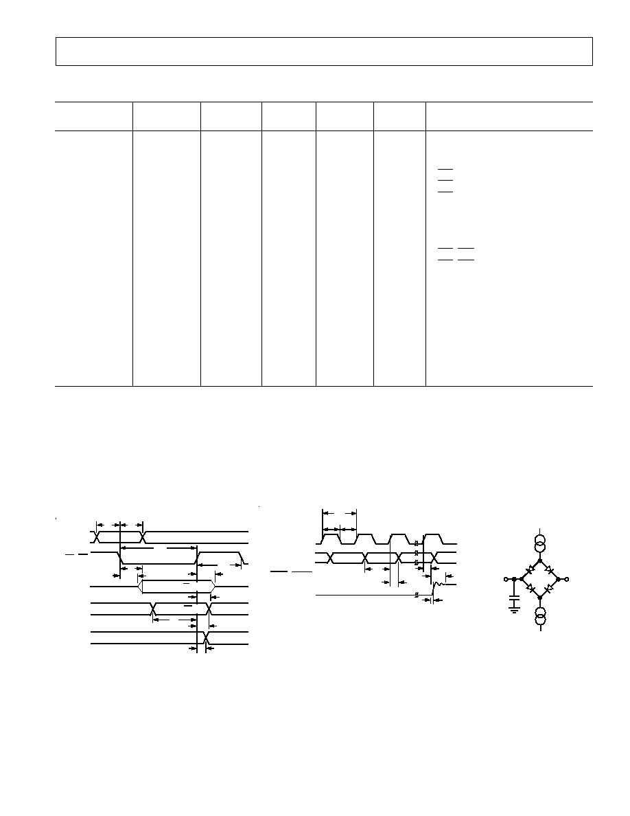
RS0, RS1,
RS2
D0D7
(READ)
D0D7
(WRITE)
RD, WR
DATA OUT (RD = 0)
DATA IN (WR = 0)
VALID
CR0CR3
t
4
t
3
t
1
t
2
t
10
t
5
t
11
t
6
t
8
t
7
t
9
Figure 1. MPU Read/Write Timing
DATA
IOR, IOG, IOB
NOTES
1. OUTPUT DELAY MEASURED FROM THE 50% POINT OF THE RISING EDGE
OF CLOCK TO THE 50% POINT OF FULL-SCALE TRANSITION.
2. SETTLING TIME MEASURED FROM THE 50% POINT OF FULL-SCALE
TRANSITION TO THE OUTPUT REMAINING WITHIN
±
1 LSB.
3. OUTPUT RISE/FALL TIME MEASURED BETWEEN THE 10% AND 90%
POINTS OF FULL-SCALE TRANSITION.
CLOCK
R0-R7, G0G7,
B0B7,
OL0-OL3, S0S1,
SYNC, BLANK
t
14
t
16
t
15
t
12
t
19
t
18
t
13
t
17
Figure 2. Video Input/Output Timing
3.2mA
+2.1V
TO
OUTPUT
PIN
50pF
400
µ
A
Figure 3. Load Circuit for Bus
Access and Relinquish Time
ADV473
4
REV. A
RECOMMENDED OPERATING CONDITIONS
Parameter
Symbol
Min
Typ
Max
Units
Power Supply
V
AA
4.75
5.00
5.25
Volts
Ambient Operating Temperature
T
A
0
+70
°
C
Output Load
R
L
37.5
Reference Voltage
V
REF
1.14
1.235
1.26
Volts
CAUTION
ESD (electrostatic discharge) sensitive device. Electrostatic charges as high as 4000 V readily
accumulate on the human body and test equipment and can discharge without detection.
Although the ADV473 features proprietary ESD protection circuitry, permanent damage may
occur on devices subjected to high energy electrostatic discharges. Therefore, proper ESD
precautions are recommended to avoid performance degradation or loss of functionality.
The ADV473 is capable of generating RGB video output sig-
nals, without requiring external buffering, and which are com-
patible with RS-343A and RS-170 video standards. All digital
inputs and outputs are TTL compatible.
The part can be driven by the on-board voltage reference or an
external voltage reference.
The part is packaged in a 68-pin Plastic Leaded Chip Carrier
(PLCC).
(Continued from page 1)
The device consists of three, high speed, 8-bit, video D/A con-
verters (RGB), a 256 24 RAM which can be configured as a
look-up table or a linearization RAM, a 24-bit wide parallel
pixel input port and three 15 8 overlay registers. The part is
controlled through the MPU port by the various on-board con-
trol/command registers.
The individual red, green and blue pixel input ports allow true-
color, image rendition. True-color image rendition, at speeds of
up to 135 MHz, is achieved through the 24-bit pixel input port.
The ADV473 is also capable of implementing 8-bit true color,
8-bit pseudo color and 15-bit true color.
ABSOLUTE MAXIMUM RATINGS
1
V
AA
to GND . . . . . . . . . . . . . . . . . . . . . . . . . . . . . . . . . . . 7 V
Voltage on Any Digital Pin . . . . GND 0.5 V to V
AA
+ 0.5 V
Ambient Operating Temperature (T
A
) . . . . . 55
°
C to +125
°
C
Storage Temperature (T
S
) . . . . . . . . . . . . . . 65
°
C to +150
°
C
Junction Temperature (T
J
) . . . . . . . . . . . . . . . . . . . . +150
°
C
Lead Temperature (Soldering, 10 secs) . . . . . . . . . . . +300
°
C
Vapor Phase Soldering (2 minutes) . . . . . . . . . . . . . . +220
°
C
IOR, IOG, IOB to GND
2
. . . . . . . . . . . . . GND0.5 V to V
AA
NOTES
1
Stresses above those listed under "Absolute Maximum Ratings" may cause
permanent damage to the device. This is a stress rating only and functional
operation of the device at these or any other conditions above those listed in the
operational sections of this specification is not implied. Exposure to absolute
maximum rating conditions for extended periods may affect device reliability.
2
Analog output short circuit to any power supply or common can be of an indefinite
duration.
ORDERING GUIDE
Temperature
No. of Package
Model
Speed
Range
Pins
Option*
ADV473KP135 135 MHz 0
°
C to +70
°
C
68
P-68A
ADV473KP110 110 MHz 0
°
C to +70
°
C
68
P-68A
ADV473KP80
80 MHz
0
°
C to +70
°
C
68
P-68A
ADV473KP66
66 MHz
0
°
C to +70
°
C
68
P-68A
NOTE
*
All devices are packaged in a 68-pin plastic leaded (J-lead) chip carrier.
WARNING!
ESD SENSITIVE DEVICE
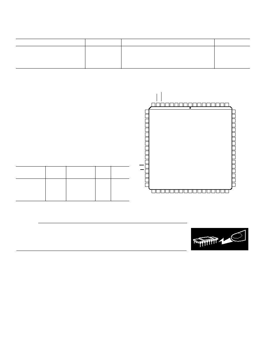
PIN CONFIGURATION
68-Pin PLCC
9
8
7
6
5
4
3
2
1
68
67
66
65
64
63
62
61
27
28
29
30
31
32
33
34
35
36
37
38
39
40
41 42
43
10
11
12
13
14
15
16
17
18
19
20
21
22
23
24
25
26
TOP VIEW
(Not To Scale)
ADV473
OL0
OL1
OL2
OL3
D0
D1
D2
D3
D4
D5
D6
D7
RS0
RS1
RS2
WR
RD
CR1
GND
GND
IOG
CR0
CR2
CR3
IOR
IOB
COMP
R
SET
V
REFIN
COMP
V
AA
V
AA
V
AA
V
AA
CLOCK
BLANK
SI
S0
GND
GND
B7
B6
B5
B4
B3
B2
B1
B0
SYNC
V
AA
V
AA
G7
G6
G5
G4
G3
G2
G1
G0
R7
R6
R5
R4
R3
R2
R1
R0
V
REFOUT
59
58
57
56
55
54
53
52
51
50
49
48
47
46
45
44
60

ADV473
5
REV. A
PIN FUNCTION DESCRIPTION
BLANK
Composite Blank Control Input (TTL Compatible). A logic zero drives the analog outputs to the blanking level.
It is latched on the rising edge of CLOCK. When BLANK is a logical zero, the pixel and overlay inputs are
ignored.
SYNC
Composite SYNC Control Input (TTL Compatible). A logical zero on this input switches off a 40 IRE current
source on the analog outputs. SYNC does not override any other control or data input; therefore, it should be
asserted only during the blanking interval. It is latched on the rising edge of CLOCK. If sync information is not
required on the analog outputs, SYNC should be connected to ground.
CLOCK
Clock Input (TTL Compatible). The rising edge of CLOCK latches the R0R7, G0G7, B0B7, S0, S1,
OL0OL3, SYNC, and BLANK inputs. It is typically the pixel clock rate of the video system. It is
recommended that CLOCK be driven by a dedicated TTL buffer.
R0R7
Red, Green and Blue Select Inputs (TTL Compatible). These inputs specify, on a pixel basis, the color value to
B0B7
be written to the DACs. They are latched on the rising edge of CLOCK. R0, G0 and B0 are the LSBs. Unused
G0G7
inputs should be connected to GND.
S0, S1
Color Mode Select Inputs (TTL Compatible). These inputs specify the mode of operation as shown in Table III.
They are latched on the rising edge of CLOCK.
OL0OL3
Overlay Select Inputs (TTL Compatible). These inputs specify which palette is to be used to provide color
information. When accessing the overlay palette, the R0R7, G0G7, B0B7, S0 and S1 inputs are ignored. They
are latched on the rising edge of CLOCK. OL0 is the LSB. Unused inputs should be connected to GND.
IOR, IOG, IOB
Red, Green, and Blue Current Outputs. These high impedance current sources are capable of directly driving a
doubly terminated 75
coaxial cable.
R
SET
Full-Scale Adjust Resistor. A resistor (R
SET
) connected between this pin and GND controls the magnitude of the
full-scale video signal. The relationship between R
SET
and the full-scale output current on each output is:
R
SET
(
) = 3,195
×
V
REF
(V)/I
OUT
(mA) SETUP = 7.5 IRE)
R
SET
(
) = 3,025
×
V
REF
(V)/I
OUT
(mA) SETUP = 0 IRE)
COMP
Compensation Pin. These pins should be connected together at the chip and connected through 0.1
µ
F ceramic
capacitor to V
AA
.
V
REFIN
Voltage Reference Input. This input requires a 1.2 V reference voltage. This is achieved through the on-board
voltage reference generator by connecting V
REFOUT
to V
REFIN
. If an external reference is used, it must supply
this input with a 1.2 V (typical) reference.
V
REFOUT
Voltage Reference Output. This output delivers a 1.2 V reference voltage from the device's on-board voltage
reference generator. It is normally connected directly to the V
REFIN
pin. If it is preferred to use an external
voltage reference, this pin may be left floating. Up to four ADV473s can be driven from V
REFOUT
.
V
AA
Analog power. All V
AA
pins must be connected.
GND
Analog Ground. All GND pins must be connected.
WR
Write Control Input (TTL Compatible). D0D7 data is latched on the rising edge of WR, and RS0RS2 are
latched on the falling edge of WR during MPU write operations. RD and WR should not be asserted
simultaneously.
RD
Read Control Input (TTL Compatible). To read data from the device, RD must be a logical zero. RS0RS2 are
latched on the falling edge of RD during MPU read operations. RD and WR should not be asserted
simultaneously.
RS0, RS1, RS2
Register Select Inputs (TTL Compatible). RS0RS2 specify the type of read or write operation being performed.
D0D7
Data Bus (TTL Compatible). Data is transferred into and out of the device over this eight-bit bidirectional data
bus. D0 is the least significant bit.
CR0CR7
Control Outputs (TTL Compatible). These outputs are used to control application specific features. The output
values are determined by the contents of the command register (CR).
ADV473
6
REV. A
CIRCUIT DESCRIPTION
MPU Interface
The ADV473 supports a standard MPU bus interface, allowing
the MPU direct access to the color palette RAM and overlay
color registers.
Three address decode lines, RS0RS2, specify whether the
MPU is accessing the address register, the color palette RAM,
the overlay registers, or read mask register. These controls also
determine whether this access is a read or write function. Table
I illustrates this decoding. The 8-bit address register is used to
address the contents of the color palette RAM and overlay
registers.
Table I. Control Input Truth Table
RS2
RS1
RS0
Addressed by MPU
0
0
0
Address Register (RAM Write Mode)
0
1
1
Address Register (RAM Read Mode)
0
0
1
Color Palette RAM
0
1
0
Pixel Read Mask Register
1
0
0
Address Register (Overlay Write Mode)
1
1
1
Address Register (Overlay Read Mode)
1
0
1
Overlay Registers
1
1
0
Command Register
Color Palette Writes
The MPU writes to the address register (selecting RAM write
mode, RS2 = 0, RS1 = 0 and RS0 = 0) with the address of the
color palette RAM location to be modified. The MPU performs
three successive write cycles (8 or 6 bits each of red, green, and
blue), using RS0RS2 to select the color palette RAM (RS2 =
0, RS1 = 0, RS0 = 1). After the BLUE write cycle, the three
bytes of color information are concatenated into a 24-bit word
or an 18-bit word and written to the location specified by the
address register. The address register then increments to the
next location which the MPU may modify by simply writing an-
other sequence of red, green, and blue data. A complete set of
colors can be loaded into the palette by initially writing the start
address and then performing a sequence of RED, GREEN and
BLUE writes. The address automatically increments to the next
highest location after a BLUE write.
Color Palette Reads
The MPU writes to the address register (selecting RAM read
mode, RS2 = 0, RS1 = 1 and RS0 = 1) with the address of the
color palette RAM location to be read back. The contents of the
palette RAM are copied to the RED, GREEN and BLUE regis-
ters and the address register increments to point to the next pal-
ette RAM location. The MPU then performs three successive
read cycles (8 or 6 bits each of red, green, and blue), using
RS0RS2 to select the color palette RAM (RS2 = 0, RS1 = 0,
RS0 = 1). After the BLUE read cycle, the 24/18 bit contents of
the palette RAM at the location specified by the address register
is loaded into the RED, GREEN and BLUE registers. The ad-
dress register then increments to the next location which the
MPU can read back by simply reading another sequence of red,
green, and blue data. A complete set of colors can be read back
from the palette by initially writing the start address and then
performing a sequence of RED, GREEN and BLUE reads. The
address automatically increments to the next highest location
after a BLUE read.
TERMINOLOGY
BLANKING LEVEL
The level separating the SYNC portion from the video portion
of the waveform. Usually referred to as the front porch or back
porch. At 0 IRE units, it is the level which will shut off the pic-
ture tube, resulting in the blackest possible picture.
COLOR VIDEO (RGB)
This usually refers to the technique of combining the three pri-
mary colors of red, green and blue to produce color pictures
within the usual spectrum. In RGB monitors, three DACs are
required, one for each color.
COMPOSITE SYNC SIGNAL (SYNC)
The position of the composite video signal which synchronizes
the scanning process.
COMPOSITE VIDEO SIGNAL
The video signal with or without setup, plus the composite
SYNC
signal.
GRAY SCALE
The discrete levels of video signal between reference black and
reference white levels. An 8-bit DAC contains 256 different lev-
els while a 6-bit DAC contains 64.
RASTER SCAN
The most basic method of sweeping a CRT one line at a time to
generate and to display images.
REFERENCE BLACK LEVEL
The maximum negative polarity amplitude of the video signal.
REFERENCE WHITE LEVEL
The maximum positive polarity amplitude of the video signal.
SETUP
The difference between the reference black level and the blank-
ing level.
SYNC
LEVEL
The peak level of the composite SYNC signal.
VIDEO SIGNAL
That portion of the composite video signal which varies in gray
scale levels between reference white and reference black. Also
referred to as the picture signal, this is the portion which may be
visually observed.
ADV473
7
REV. A
Table II. Address Register (ADDR) Operation
Value
RS2
RS1
RS0
Addressed by MPU
ADDRa,b (Counts Modulo 3)
00
X
0
1
Red Value
01
X
0
1
Green Value
10
X
0
1
Blue Value
ADDR0-7 (Counts Binary)
00HFFH
0
0
1
Color Palette RAM
XXXX 0000
1
0
1
Reserved
XXXX 0001
1
0
1
Overlay Color 1
XXXX 0010
1
0
1
Overlay Color 2
·
·
·
·
·
·
·
·
·
·
XXXX 1111
1
0
1
Overlay Color 15
Overlay Color Writes
The MPU writes to the address register (selecting OVERLAY
REGISTER write mode, RS2 = 1, RS1 = 0 and RS0 = 0) with
the address of the overlay register to be modified. The MPU
performs three successive write cycles (8 or 6 bits each of red,
green, and blue), using RS0RS2 to select the Overlay Registers
(RS2 = 1, RS1 = 0, RS0 = 1). After the BLUE write cycle, the
three bytes of color information are concatenated into a 24-bit
word or an 18-bit word and are written to the overlay register
specified by the address register. The address register then in-
crements to the next overlay register which the MPU may
modify by simply writing another sequence of red, green, and
blue data. A complete set of colors can be loaded into the over-
lay registers by initially writing the start address and then per-
forming a sequence of RED, GREEN and BLUE writes. The
address automatically increments to the next highest location
after a BLUE write.
Overlay Color Reads
The MPU writes to the address register (selecting OVERLAY
REGISTER read mode, RS2 = 1, RS1 = 1 and RS0 = 1) with
the address of the overlay register to be read back. The contents
of the overlay register are copied to the RED, GREEN and
BLUE registers and the address register increments to point to
the next highest overlay register. The MPU then performs three
successive read cycles (8 or 6 bits each of red, green, and blue),
using RS0 RS2 to select the Overlay Registers (RS2 = 1, RS1
= 0, RS0 = 1). After the BLUE read cycle, the 24/18 bit con-
tents of the overlay register at the specified address register loca-
tion is loaded into the RED, GREEN and BLUE registers. The
address register then increments to the next overlay register
which the MPU can read back by simply reading another se-
quence of red, green, and blue data. A complete set of colors
can be read back from the overlay registers by initially writing
the start address and then performing a sequence of RED,
GREEN and BLUE reads. The address automatically
incremeets to the next highest location after a BLUE read.
Internal Address Register (ADDR)
When accessing the color palette RAM, the address register
resets to 00H following a blue read or write cycle to RAM loca-
tion FFH. When accessing the overlay color registers, the
address register increments following a blue read or write cycle.
However, while accessing the overlay color registers, the four
most significant bits (since there are only 15 overlay registers) of
the address register (ADDR47) are ignored.
To keep track of the red, green, and blue read/write cycles, the
address register has two additional bits (ADDRa, ADDRb) that
count modulo three, as shown in Table II. They are reset to
zero when the MPU writes to the address register, and are not
reset to zero when the MPU reads the address register. The
MPU does not have access to these bits. The other eight bits of
the address register, incremented following a blue read or write
cycle, (ADDR0-7) are accessible to the MPU, and are used to
address color palette RAM locations and overlay registers, as
shown in Table II. ADDR0 is the LSB when the MPU is access-
ing the RAM or overlay registers. The MPU may read the ad-
dress register at any time without modifying its contents or the
existing read/write mode.
Synchronization
The MPU interface operates asynchronously to the pixel port.
Data transfers between the color palette RAM/overlay registers
and the color registers (R, G, and B as shown in the block dia-
gram) are synchronized by internal logic, and occur in the pe-
riod between MPU accesses. The MPU can be accessed at any
time, even when the pixel CLOCK is stopped.
8-Bit/6-Bit Color Operation
The Command Register on the ADV473 specifies whether the
MPU is reading/writing 8 bits or 6 bits of color information
each cycle.
For 8-bit operation, D0 is the LSB and D7 is the MSB.
For 6-bit operation, color data is contained on the lower six bits
of the data bus, with D0 being the LSB and D5 the MSB of
color data. When writing color data, D6 and D7 are ignored.
During color read cycles, D6 and D7 will be a logical "0." It
should be noted that when the ADV473 is in 6-bit mode, full-
scale output current will be reduced by approximately 1.5%
relative to the 8-bit mode. This is the case since the 2 LSBs of
each of the three DACs are always set to zero in 6-bit mode.
ADV473
8
REV. A
Command Register (CR)
The ADV473 has an internal command register (CR). This reg-
ister is 8 bits wide, CR0CR7 and is directly mapped to the
MPU data bus on the part, D0D7. The command register can
be written to or read from. It is not initialized, therefore it must
be set. Figure 4 shows what each bit of the CR register controls
and shows the values it must be programmed to for various
modes of operation.
Color Modes
The ADV473 supports four color modes, 24-bit true-color,
15-bit true-color, 8-bit true-color and 8-bit pseudo-color. The
mode of operation is determined by the S0 and S1 inputs, in
conjunction with CR7 and CR6 of the command register. S0
and S1 are pipelined to maintain synchronization with the video
data. Table III illustrates the modes of operation.
Table III. Color Operation Modes
OL3OL0
S1, S0
CR7, CR6
Mode
R7R0
G7G0
B7B0
1111
XX
XX
Overlay Color 15
XXH
XXH
XXH
.
.
.
.
.
.
.
.
.
.
.
.
.
.
0001
XX
XX
Overlay Color 1
XXH
XXH
XXH
0000
00
00
24-Bit True-Color
R7R0
G7G0
B7B0
0000
00
01
24-Bit True-Color
R7R0
G7G0
B7B0
0000
00
10
24-Bit True-Color
R7R0
G7G0
B7B0
0000
00
11
Reserved
Reserved
Reserved
Reserved
0000
01
00
24-Bit True-Color Bypass
R7R0
G7G0
B7B0
0000
01
01
24-Bit True-Color Bypass
R7R0
G7G0
B7B0
0000
01
10
24-Bit True-Color Bypass
R7R0
G7G0
B7B0
0000
01
11
Reserved
Reserved
Reserved
Reserved
0000
10
00
8-Bit Pseudo-Color (Red)
P7P0
Ignored
Ignored
0000
10
01
8-Bit Pseudo-Color (Green)
Ignored
P7P0
Ignored
0000
10
10
8-Bit Pseudo-Color (Blue)
Ignored
Ignored
P7P0
0000
10
11
15-Bit True-Color
Orrrrrgg
gggbbbbb
Ignored
0000
11
00
8-Bit True-Color Bypass (Red)
rrrgggbb
Ignored
Ignored
0000
11
01
8-Bit True-Color Bypass (Green)
Ignored
rrrgggbb
Ignored
0000
11
10
8-Bit True-Color Bypass (Blue)
Ignored
Ignored
rrrgggbb
0000
11
11
15-Bit True-Color Bypass
Orrrrrgg
gggbbbbb
Ignored
X = Don't Care
CONTROL OUTPUTS
THESE BITS ARE OUTPUT
ONTO THE CR3-CR0 PINS
CR5
0
1
0 IRE
7.5 IRE
PEDESTAL ENABLE
CONTROL (SETUP)
CR4
0
1
6-BIT
8-BIT
8-BIT/6-BIT
COLOR SELECT
COLOR MODE
SELECT
(SEE TABLE III)
CR5
CR4
CR3
CR2
CR1
CR7
CR6
CR0
Figure 4. Command Register (CR)
ADV473
9
REV. A
15-Bit True-Color Bypass Mode
Fifteen bits of pixel information may be input into the ADV473
every clock cycle. The 15 bits of pixel information (5 bits of red,
5 bits of green, and 5 bits of blue) are input via the R0R7 and
G0G7 inputs.
Table V. 15-Bit True-Color Video Input Format
Pixel
Input
Inputs
Format
R7
0
R6
R7
R5
R6
R4
R5
R3
R4
R2
R3
R1
G7
R0
G6
G7
G5
G6
G4
G5
G3
G4
B7
G3
B6
G2
B5
G1
B4
G0
B3
The 5 MSBs of the red, green, and blue DACs are driven di-
rectly by the inputs. The 3 LSBs are a logical zero. The color
palette RAMs and pixel read mask register are bypassed.
15-Bit True-Color Mode
Fifteen bits of pixel information may be input into the ADV473
every clock cycle. The 15 bits of pixel information are input to
the device via R0R7 and G0G7 according to Table V. This
input data points to the top 32 locations of the color palette
RAM, i.e., locations 223 to 255. The 15-bit pixel input data in-
dexes a 24-bit red, green and blue value which is clocked to the
three DACs.
Overlays
The overlay inputs, OL0OL3, have priority regardless of the
color mode as shown in Table III.
Pixel Read Mask Register
The 8-bit pixel read mask register is implemented as three 8-bit
pixel read mask registers, one each for the R0R7, G0G7, and
B0B7 inputs. When writing to the pixel read mask register, the
same data is written to all three registers. The read mask regis-
ters are located just before the color palette RAMs. Thus, they
are used only in the 24-bit true-color and 8-bit pseudo-color
modes since these are the only modes that use the color palette
RAMs.
The contents of the pixel read mask register, which may be
accessed by the MPU at any time, are bit-wise logically ANDed
with the 8-bit inputs prior to addressing the color palette RAMs.
Bit D0 of the pixel read mask register corresponds to pixel input
P0 (R0, G0, or B0 depending on the mode). Bit D0 also corre-
sponds to data bus Bit D0.
VIDEO MODES
24-Bit True-Color Mode
Twenty-four bits of RGB color information may be input into
the ADV473 every clock cycle. The 24 bits of pixel information
are input via the R0R7, G0G7, and B0B7 inputs. R0R7 ad-
dress the red color palette RAM, G0G7 address the green
color palette RAM, and B0B7 address the blue color palette
RAM. Each RAM provides 8 bits of color information to the
corresponding D/A converter. The pixel read mask register is
used in this mode.
24-Bit True-Color Bypass Mode
Twenty-four bits of pixel information may be input into the
ADV473 every clock cycle. The 24 bits of pixel information are
input via the R0R7, G0G7, and B0B7 inputs. R0R7 drive
the red DAC directly, G0G7 drive the green DAC directly,
and B0B7 drive the blue DAC directly. The color palette
RAMs and pixel read mask register are bypassed.
8-Bit Pseudo-Color Mode
Eight bits of pixel information may be input into the ADV473
every clock cycle. The 8 bits of pixel information (P0P7) are
input via the R0R7, G0G7 or B0B7 inputs, as specified by
CR7 and CR6. All three color palette RAMs are addressed by
the same 8 bits of pixel data (P0P7). Each RAM provides 8
bits of color information to the corresponding D/A converter.
The pixel read mask register is used in this mode.
8-Bit True-Color Bypass Mode
Eight bits of pixel information may be input into the ADV473
every clock cycle. The 8 bits of pixel information are input via
the R0R7, G0G7 or B0B7 inputs, as specified by CR7 and
CR6.
Table IV. 8-Bit True-Color Bypass Video Input Format
R0R7
G0G7
B0B7
Inputs
Inputs
Input
Inputs
Selected
Selected
Selected
Format
R7
G7
B7
R7
R6
G6
B6
R6
R5
G5
B5
R5
R4
G4
B4
G7
R3
G3
B3
G6
R2
G2
B2
G5
R1
G1
B1
B7
R0
G0
B0
B6
As seen in the table, 3 bits of red, 3 bits of green, and 2 bits of
blue data are input. The 3 MSBs of the red and green DACs are
driven directly by the inputs, while the 2 MSBs of the blue DAC
are driven directly. The 5 LSBs for the red and green DACs,
and the 6 LSBs for the blue DAC, are a logical zero. The color
palette RAMs and pixel read mask register are bypassed.
ADV473
10
REV. A
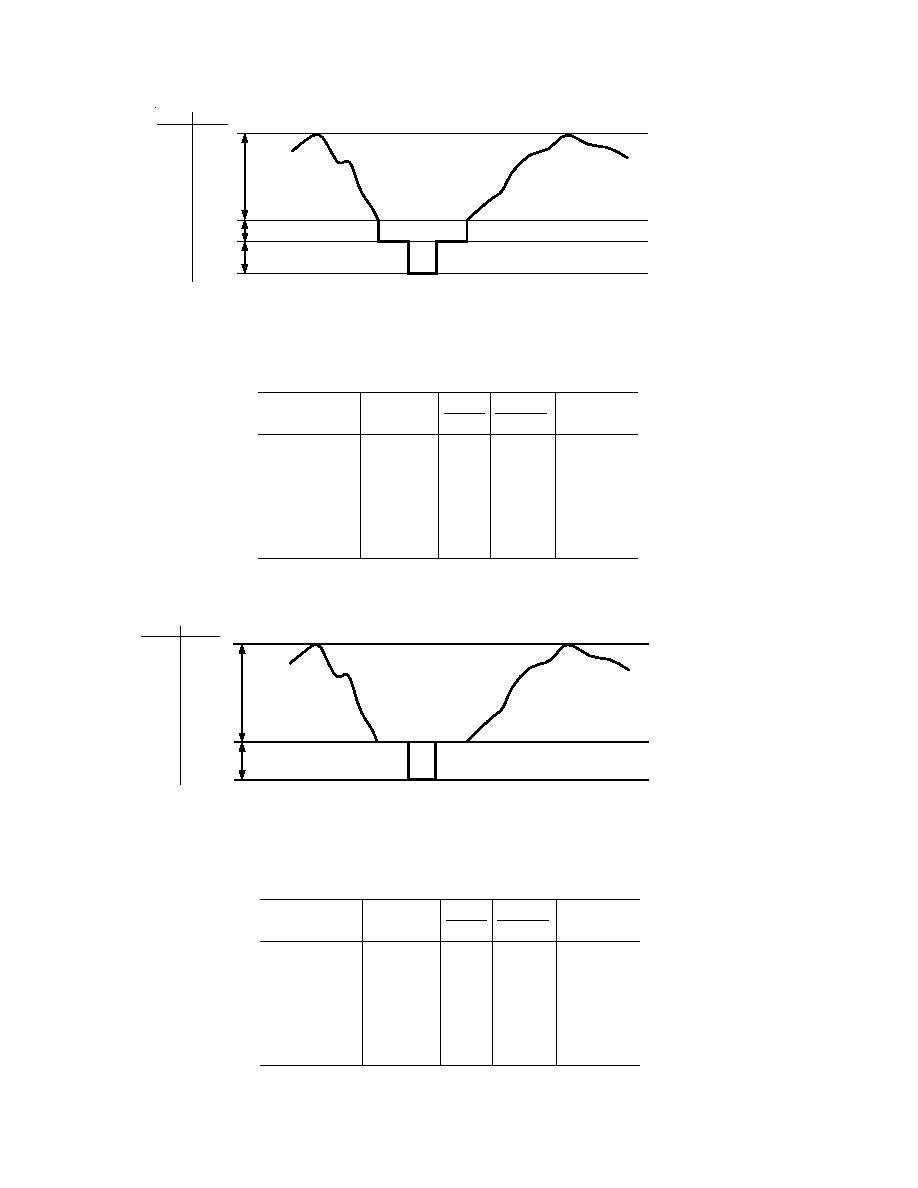
7.5 IRE
SYNC LEVEL
BLANK LEVEL
BLACK LEVEL
WHITE LEVEL
26.67
1.000
9.05
0.340
7.62
0.286
0.000
0.00
MA
V
92.5 IRE
40 IRE
NOTE:
75
DOUBLY TERMINATED LOAD, SETUP = 7.5 IRE, V
REF
= 1.235 V, R
SET
= 140
RS-343A LEVELS AND TOLERANCES ASSUMED ON ALL LEVELS.
Figure 5. Composite Video Output Waveform (Setup = 7.5 IRE)
Table VI. Video Output Truth Table (Setup = 7.5 IRE)
I
OUT
DAC
Description
(mA)
SYNC BLANK
Input Data
WHITE
26.67
1
1
FFH
DATA
Data+9.05
1
1
Data
DATA-SYNC
Data+1.44
0
1
Data
BLACK
9.05
1
1
00H
BLACK-SYNC
1.44
0
1
00H
BLANK
7.62
1
0
XXH
SYNC
0
0
0
XXH
NOTE
Typical with full-scale IOR, IOG, IOB = 26.67 mA, SETUP = 7.5 IRE,
V
REF
= 1.235 V, R
SET
= 140
. External voltage reference adjusted for
26.67 mA full-scale output.
25.24
0.950
7.62
0.286
0.000
0.00
MA
V
SYNC LEVEL
BLACK/BLANK
LEVEL
WHITE LEVEL
100 IRE
43 IRE
NOTE:
75
DOUBLY TERMINATED LOAD, SETUP = 0 IRE, V
REF
= 1.235 V, R
SET
= 140
RS-343A LEVELS AND TOLERANCES ASSUMED ON ALL LEVELS.
Figure 6. Composite Video Output Waveform (Setup = 0 IRE)
Table VII. Video Output Truth Table (SETUP = 0 IRE)
I
OUT
DAC
Description
(mA)
SYNC BLANK
Input Data
WHITE
25.24
1
1
FFH
DATA
Data+7.62
1
1
Data
DATA-SYNC
Data
0
1
Data
BLACK
7.62
1
1
00H
BLACK-SYNC
0
0
1
00H
BLANK
7.62
1
0
XXH
SYNC
0
0
0
XXH
NOTE
Typical with full-scale IOR, IOG, IOB = 25.24 mA, SETUP = 0 IRE,
V
REF
= 1.235 V, R
SET
= 140
. External voltage reference adjusted for
26.67 mA full-scale output.
ADV473
11
REV. A
PC BOARD LAYOUT CONSIDERATIONS
The layout should be optimized for lowest noise on the ADV473
power and ground lines by shielding the digital inputs and pro-
viding good decoupling. The lead length between groups of V
AA
and GND pins should be minimized so as to minimize inductive
ringing.
Ground Planes
The ground plane should encompass all ADV473 ground pins,
current/voltage reference circuitry, power supply bypass circuitry
for the ADV473, the analog output traces, and all the digital sig-
nal traces leading up to the ADV473.
Power Planes
The ADV473 and any associated analog circuitry should have its
own power plane, referred to as the analog power plane. This
power plane should be connected to the regular PCB power
plane (V
CC
) at a single point through a ferrite bead, as illustrated
in Figures 7 and 8. This bead should be located within three
inches of the ADV473.
The PCB power plane should provide power to all digital logic
on the PC board, and the analog power plane should provide
power to all ADV473 power pins and voltage reference circuitry.
Plane-to-plane noise coupling can be reduced by ensuring that
portions of the regular PCB power and ground planes do not
overlay portions of the analog power plane, unless they can be
arranged such that the plane-to-plane noise is common mode.
Supply Decoupling
For optimum performance, bypass capacitors should be installed
using the shortest leads possible, consistent with reliable opera-
tion, to reduce the lead inductance. Best performance is ob-
tained with a 0.1
µ
F ceramic capacitor decoupling each of the
two groups of V
AA
pins to GND. These capacitors should be
placed as close as possible to the device.
It is important to note that while the ADV473 contains circuitry
to reject power supply noise, this rejection decreases with fre-
quency. If a high frequency switching power supply is used, the
designer should pay close attention to reducing power supply
noise and should consider using a three-terminal voltage regula-
tor for supplying power to the analog power plane.
Digital Signal Interconnect
The digital inputs to the ADV473 should be isolated as much as
possible from the analog outputs and other analog circuitry.
Also, these input signals should not overlay the analog power
plane.
Due to the high clock rates involved, long clock lines to the
ADV473 should be avoided to reduce noise pickup.
Any active termination resistors for the digital inputs should be
connected to the regular PCB power plane (V
CC
), and not to the
analog power plane.
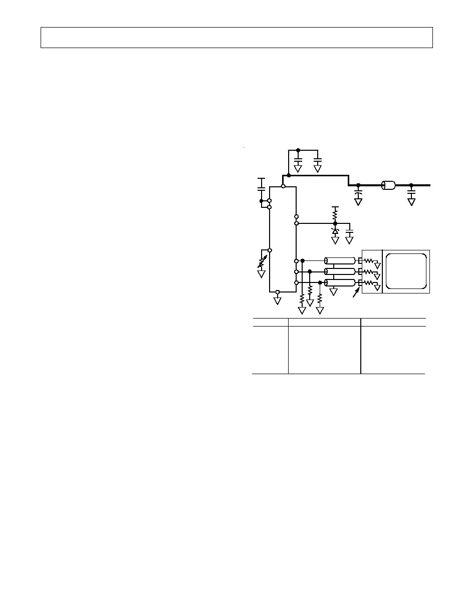
ANALOG POWER PLANE
IOR
IOG
IOB
V
AA
ADV473
V
REFIN
75
75
V
REFOUT
CO-AXIAL CABLE
(75
)
GND
BNC
CONNECTORS
75
75
75
MONITOR
(CRT)
0.1
µ
F
10
µ
F
POWER SUPPLY DECOUPLING
(0.1
µ
F CAPACITOR FOR
EACH V
REF
GROUP)
0.1
µ
F
L1
(FERRITE
BEAD)
COMP
COMP
+5V (V
AA
)
0.1
µ
F
+5V (V
AA
)
+5V (V
CC
)
+5V (V
AA
)
0.1
µ
F
1k
(1% METAL)
AD589
(1.2 V
REF
)
COMPONENT
DESCRIPTION
VENDOR PART NUMBER
C1 C5
0.1
µ
F CERAMIC CAPACITOR
ERIE RPE112Z5U104M50V
C6
10
µ
F TANTALUM CAPACITOR
MALLORY CSR13G106KM
L1
FERRITE BEAD
FAIR-RITE 2743001111
R1, R2, R3
75
1% METAL FILM RESISTOR
R4
1k
5% RESISTOR
R
SET
1% METAL FILM RESISTOR
Z1
1.23V VOLTAGE REFERENCE
AD589JN
R
SET
140
R
SET
0.1
µ
F
75
Figure 7. Typical Connection Diagram (External Voltage
Reference)
ADV473
12
REV. A
C1761241/93
PRINTED IN U.S.A.
Analog Signal Interconnect
The ADV473 should be located as close as possible to the out-
put connectors to minimize noise pickup and reflections due to
impedance mismatch.
The video output signals should overlay the ground plane, and
not the analog power plane, to maximize the high frequency
power supply rejection.
For maximum performance, the analog outputs should each
have a 75
load resistor connected to GND. The connection
between the current output and GND should be as close as pos-
sible to the ADV473 to minimize reflections.
For more information on circuit board design and layout, see
application note entitled "Design and Layout of a Video Graph-
ics System for Reduced EMI" available from Analog Devices,
Publication No. E1309-15-10/89.
COMPONENT
DESCRIPTION
VENDOR PART NUMBER
C1 C5
0.1
µ
F CERAMIC CAPACITOR
ERIE RPE112Z5U104M50V
C6
10
µ
F TANTALUM CAPACITOR
MALLORY CSR13G106KM
L1
FERRITE BEAD
FAIR-RITE 2743001111
R1, R2, R3
75
1% METAL FILM RESISTOR
R
SET
1% METAL FILM RESISTOR
0.1
µ
F
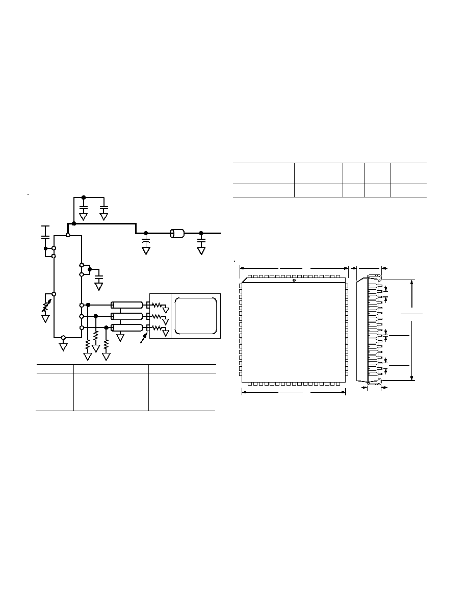
ANALOG POWER PLANE
IOR
IOG
IOB
V
AA
ADV473
V
REFIN
75
75
V
REFOUT
CO-AXIAL CABLE
(75
)
GND
BNC
CONNECTORS
75
75
75
MONITOR
(CRT)
0.1
µ
F
10
µ
F
POWER SUPPLY DECOUPLING
(0.1
µ
F CAPACITOR FOR
EACH V
REF
GROUP)
0.1
µ
F
L1
(FERRITE
BEAD)
COMP
COMP
+5V (V
AA
)
0.1
µ
F
+5V (V
AA
)
+5V (V
CC
)
R
SET
140
R
SET
0.1
µ
F
75
Figure 8. Typical Connection Diagram (Internal Voltage
Reference)
Package Thermal Considerations
In certain circumstances, the 135 MHz version of the ADV473
may require forced air cooling or the addition of a heatsink. The
68-pin PLCC has a heat resistance characteristic as shown in
Table VIII.
It should be noted that information on Package Thermal Characteris-
tics published herein may not be the most up to date at the time of
reading this. Advances in packaging technology will inevitably lead
to improvements in thermal data. Please contact your local sales office
for the most up-to-date information.
Table VIII. Thermal Resistance vs. Airflow
Air Velocity
(Linear Feet/Min)
0 (Still Air)
50
100
200
JA
(
°
C/W)
32
26
19
16
OUTLINE DIMENSIONS
Dimensions shown in inches and (mm).
Plastic Leaded Chip Carrier
(P-68A)
0.954 (24.23)
0.950 (24.13)
SQ
0.995 (25.27)
0.885 (22.48)
SQ
61
10
44
9
43
26
60
TOP VIEW
PIN 1
IDENTIFIER
27
0.029 (0.74)
0.027 (0.69)
0.019 (0.48)
0.017 (0.43)
0.175 (4.45)
0.169 (4.29)
0.925 (23.50)
0.895 (22.73)
0.104 (2.64) TYP
0.050
(1.27)
TYP