 | ÐлекÑÑоннÑй компоненÑ: ADV612 | СкаÑаÑÑ:  PDF PDF  ZIP ZIP |
ADV611/612 Data Sheet (1-24)
REV. 0
Information furnished by Analog Devices is believed to be accurate and
reliable. However, no responsibility is assumed by Analog Devices for its
use, nor for any infringements of patents or other rights of third parties
which may result from its use. No license is granted by implication or
otherwise under any patent or patent rights of Analog Devices.
a
ADV611/ADV612
One Technology Way, P.O. Box 9106, Norwood, MA 02062-9106, U.S.A.
Tel: 781/329-4700
World Wide Web Site: http://www.analog.com
Fax: 781/326-8703
© Analog Devices, Inc., 1999
Closed Circuit TV Digital
Video Codec
FUNCTIONAL BLOCK DIAGRAM
QUANTIZER
& ENTROPY
CODING
HOST
I/O PORT
& FIFO
HOST
ADV611/
ADV612
256K 16-BIT DRAM
COMPONENT
VIDEO I/O
BIN WIDTH CONTROL
LOCATION, SIZE AND CONTRAST CONTROL
SUBBAND STATISTICS
8
16/32
DIGITAL
VIDEO
I/O PORT
WAVELET
FILTERS,
DECIMATOR &
INTERPOLATOR
QUALITY
BOX
CONTROL
ON-CHIP
TRANSFORM
BUFFER
DRAM
MANAGER
FEATURES
Programmable "Quality Box"
Industrial Temperature Range (ADV612)
Hardware Frame Rate Reduction
100% Bitstream Compatible with the ADV601 and
ADV601LC
Precise Compressed Bit Rate Control
Field Independent Compression
8-Bit Video Interface Supports CCIR-656 and Multi-
plexed Philips Formats
General Purpose 16- or 32-Bit Host Interface with
512 Deep 32-Bit FIFO
PERFORMANCE
Real-Time Compression or Decompression of CCIR-601
to Video:
720 288 @ 50 Fields/Sec -- PAL
720 243 @ 60 Fields/Sec -- NTSC
Compression Ratios from Visually Loss-Less to 7500:1
Visually Loss-Less Compression At 4:1 on Natural
Images (Typical)
APPLICATIONS
CCTV Cameras and Systems
Time-Lapse Video Tape Recorders
Time-Lapse Video Disk Recorders
Wireless CCTV Cameras
Fiber CCTV Systems
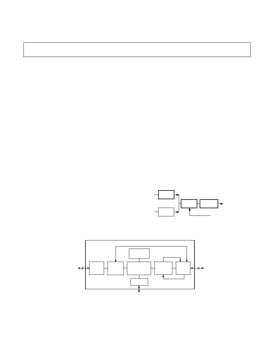
GENERAL DESCRIPTION
The ADV611/ADV612 are low cost, single chip, dedicated func-
tion, all-digital-CMOS-VLSI devices capable of supporting
visually loss-less to 7500:1 real-time compression and decom-
pression of CCIR-601 digital video at very high image quality
levels. The chips integrate glueless video and host interfaces
with on-chip SRAM to permit low part count, system level
implementations suitable for a broad range of applications.
The ADV611/ADV612 are 100% bitstream compatible with
the ADV601. The ADV611/ADV612 comes in a 120-lead
LQFP package.
The ADV611/ADV612 are video encoders/decoders optimized
for closed circuit TV (CCTV) applications. With the ADV611/
ADV612, you can define a portion of each video field to be at a
higher quality level relative to the rest of the field. This "quality
box" feature significantly increases compression of less impor-
tant background details, while retaining the image's overall
context. Additionally, the unique subband coding architecture
of the ADV611/ADV612 offer many application-specific
advantages. A review of the General Theory of Operation and
Applying the ADV611/ADV612 sections will help you get the
most use out of the ADV611/ADV612 in any given application.
The ADV611/ADV612 accept component digital video through
the Video Interface and outputs a compressed bitstream though the
Host Interface in Encode Mode. While in Decode Mode, the
ADV611/ADV612 accept compressed bitstream through the Host
Interface and outputs component digital video through the Video
Interface. The host accesses all of the ADV611/ADV612's control
and status registers using the Host Interface. Figure 2 summarizes
the basic function of the part.
(continued on page 2)
ADV7185
DECODER
ADV611/
ADV612
ADSP-21xx
ANALOG
VIDEO
SIGNAL
IMAGE
SENSOR
SIGNAL
OR
QUALITY BOX CONTROLS
FROM REMOTE SITE
SERIAL
OR PARALLEL
BITSTREAM FOR
TRANSMISSION
OR STORAGE
DIGITIZER
Figure 1. Typical Application

ADV611/ADV612
2
REV. 0
TABLE OF CONTENTS
This data sheet gives an overview of the ADV611/ADV612's
functionality and provides details on designing the part into a
system. The text of the data sheet is written for an audience with
a general knowledge of designing digital video systems. Where
appropriate, additional sources of reference material are noted
throughout the data sheet.
GENERAL DESCRIPTION . . . . . . . . . . . . . . . . . . . . . . . . . . . 1
COMPARING THE ADV6xx FAMILY VIDEO CODECS . . . . . 3
INTERNAL ARCHITECTURE . . . . . . . . . . . . . . . . . . . . . . . . 4
GENERAL THEORY OF OPERATION . . . . . . . . . . . . . . . . . . 4
References . . . . . . . . . . . . . . . . . . . . . . . . . . . . . . . . . . . . . . . . 5
THE WAVELET KERNEL . . . . . . . . . . . . . . . . . . . . . . . . . . . . 5
THE PROGRAMMABLE QUANTIZER . . . . . . . . . . . . . . . . . 8
THE RUN LENGTH CODER AND HUFFMAN CODER . . . . . 9
Encoding vs. Decoding . . . . . . . . . . . . . . . . . . . . . . . . . . . . . . 9
PROGRAMMER'S MODEL . . . . . . . . . . . . . . . . . . . . . . . . . . . 9
ADV611/ADV612 REGISTER DESCRIPTIONS . . . . . . . . . . 11
VIDEO AREA REGISTERS . . . . . . . . . . . . . . . . . . . . . . . . . . . 14
PIN FUNCTION DESCRIPTIONS . . . . . . . . . . . . . . . . . . . . 18
Video Interface . . . . . . . . . . . . . . . . . . . . . . . . . . . . . . . . . . . . 21
Video FormatsCCIR-656 . . . . . . . . . . . . . . . . . . . . . . . . . . . 22
Host Interface . . . . . . . . . . . . . . . . . . . . . . . . . . . . . . . . . . . . 23
DRAM Manager . . . . . . . . . . . . . . . . . . . . . . . . . . . . . . . . . . 23
Compressed Data-Stream Definition . . . . . . . . . . . . . . . . . . . 24
APPLYING THE ADV611/ADV612 . . . . . . . . . . . . . . . . . . . . 30
Using the ADV611/ADV612 in Computer Applications . . . . . . 30
Using the ADV611/ADV612 in Stand-Alone Applications . . . . 31
Connecting the ADV611/ADV612 to Popular Video
Decoders and Encoders . . . . . . . . . . . . . . . . . . . . . . . . . . . . 31
GETTING THE MOST OUT OF ADV611/ADV612 . . . . . . . 32
How Much Compression Can Be Expected . . . . . . . . . . . . . . 32
Evaluation Board . . . . . . . . . . . . . . . . . . . . . . . . . . . . . . . . . . 32
Software Codec . . . . . . . . . . . . . . . . . . . . . . . . . . . . . . . . . . . 32
Field Rate Reduction . . . . . . . . . . . . . . . . . . . . . . . . . . . . . . . 32
Edge Enhancement and Detection . . . . . . . . . . . . . . . . . . . . . 32
Motion Detection . . . . . . . . . . . . . . . . . . . . . . . . . . . . . . . . . 32
ADV611/ADV612 SPECIFICATIONS . . . . . . . . . . . . . . . . . . 33
TEST CONDITIONS . . . . . . . . . . . . . . . . . . . . . . . . . . . . . . . 34
TIMING PARAMETERS . . . . . . . . . . . . . . . . . . . . . . . . . . . . . 34
Clock Signal Timing . . . . . . . . . . . . . . . . . . . . . . . . . . . . . . . 34
CCIR-656 Video Format Timing . . . . . . . . . . . . . . . . . . . . . . 35
Multiplexed Philips Video Timing . . . . . . . . . . . . . . . . . . . . . 37
Host Interface (Indirect Address, Indirect Register Data,
and Interrupt Mask/Status) Register Timing . . . . . . . . . . . 40
Host Interface (Compressed Data) Register Timing . . . . . . . 42
ADV611/ADV612 LQFP PINOUTS . . . . . . . . . . . . . . . . . . . . 44
ADV611/ADV612 PIN CONFIGURATION . . . . . . . . . . . . . . 45
OUTLINE DIMENSIONS . . . . . . . . . . . . . . . . . . . . . . . . . . . . 46
ORDERING GUIDE . . . . . . . . . . . . . . . . . . . . . . . . . . . . . . . .
46
GENERAL DESCRIPTION
(Continued from page 1)
ADV611/
ADV612
VIDEO CODEC
CCTV DIGITAL
VIDEO INTERFACE
HOST INTERFACE
DIGITAL VIDEO IN
(ENCODE)
DIGITAL VIDEO
OUT (DECODE)
COMPRESSED
VIDEO OUT
(ENCODE)
COMPRESSED VIDEO
IN (DECODE)
STATUS AND CONTROL
Figure 2. Functional Block Diagram
The ADV611/ADV612 adheres to international standard
CCIR-601 for studio quality digital video. The codec also sup-
ports a range of field sizes and rates providing high performance
in computer, PAL, NTSC, or still image environments. The
ADV611/ADV612 is designed only for real-time interlaced
video; full frames of video are formed and processed as two
independent fields of data. The ADV611/ADV612 supports the
field rates and sizes in Table I. Note that the maximum active
field size is 720 by 288. The maximum pixel rate is 13.50 MHz.
The ADV611/ADV612 has a generic 16-/32-bit host interface
that includes a 512-position, 32-bit wide FIFO for compressed
video. With additional external hardware, the ADV611/ADV612's
host interface is suitable (when interfaced to other devices) for
moving compressed video over PCI, ISA, SCSI, SONET, 10 Base
T, ARCnet, HDSL, ADSL and a broad range of digital inter-
faces. For a full description of the Host Interface, see the Host
Interface section.
The compressed data rate is determined by the input data rate
and the selected compression ratio. The ADV611/ADV612 can
achieve a near constant compressed bit rate by using the current
field statistics in the off-chip bin width calculator on the exter-
nal DSP or Host. The process of calculating bin widths on a
DSP or Host can be "adaptive," optimizing the compressed bit
rate in real time. This feature provides a near constant bit rate
out of the host interface in spite of scene changes or other types
of source material changes that would otherwise create bit rate
burst conditions. For more information on the quantizer, see
the Programmable Quantizer section.
The ADV611/ADV612 typically yields visually loss-less com-
pression on natural images at a 4:1 compression ratio. For more
information on compression ratios, see the Getting the Most
Out of the ADV611/ADV612 section. Desired image quality
levels can vary widely in different applications, so it is advisable
to evaluate image quality of known source material at different
compression ratios to find the best compression range for the
application. The subband coding architecture of the ADV611/
ADV612 provides a number of options to stretch compression
performance. These options are outlined in the Applying the
ADV611/ADV612 section.
Table I. ADV611/ADV612 Field Rates and Sizes
Active
Active
Total
Total
Standard
Region
Region
Region
Region
Field Rate
Pixel Rate
Name
Horizontal
Vertical
1
Horizontal
Vertical
(Hz)
(MHz)
2
CCIR-601/525
720
243
858
262.5
59.94
13.50
CCIR-601/625
720
288
864
312.5
50.00
13.50
NOTES
1
The maximum active field size is 720 by 288.
2
The maximum pixel rate is 13.5 MHz.
ADV611/ADV612
3
REV. 0
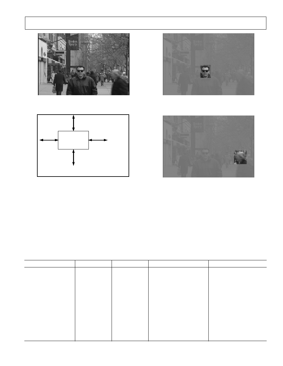
The ADV611/ADV612 are real-time compression integrated
circuits designed for remote video surveillance or closed circuit
television (CCTV) applications. The most important feature of
these two devices is the "Quality Box." With this feature the
user can define a box of any size and location within each field
of video that will be compressed at full contrast while the re-
mainder outside the box, or background of the image, is com-
pressed at a lower level of contrast. The background contrast
level is controlled by the user. The lower the contrast level, the
more the image will be compressed. The objective in a given
Table II. Differences Between the ADV601, ADV601LC, ADV611 and ADV612
ADV601
ADV601LC
ADV611
ADV612
Bits per Component
10
8
8
8
DSP Serial Port
Yes
No
No
No
Package
160 PQFP
120 LQFP
120 LQFP
120 LQFP
Pin Assignments
Unique
Unique
98% Similar to ADV601LC
98% Similar to ADV601LC
Temperature Range
0
°
C to +70
°
C
0
°
C to +70
°
C
0
°
C to +70
°
C
25
°
C to +85
°
C
JA
31
°
C/W
35
°
C/W
35
°
C/W
35
°
C/W
JC
7.5
°
C/W
5
°
C/W
5
°
C/W
5
°
C/W
Field Rate Reduction
Software
Software
Hardware
Hardware
Stall Mode
No
No
Yes
Yes
Field Truncation
No
No
Yes
Yes
Field Size Register
No
No
Yes
Yes
Field Bit Polarity Control
No
No
Yes
Yes
Evaluation Board
VideoLab
VideoPipe
CCTVPIPE
CCTVPIPE
Target Applications
Professional
Consumer
CCTV
Industrial CCTV
Figure 3.
application is to adjust the background contrast to a level that
ensures both a recognizable and useful background as well as
the highest possible compression. Figure 3 shows how this qual-
ity box appears in final video.
The ADV611/ADV612 is housed in a plastic LQFP package
suitable for cost-sensitive commercial applications.
COMPARING THE ADV6xx FAMILY VIDEO CODECS
The ADV6xx video codecs support a range of interface, pack-
age, and compression features. Table II compares these codecs:
Original Video Image
Image after compression/decompression shown
with different box size and position
PROGRAMMABLE
QUALITY BOX
VARIABLE CONTRAST
BACKGROUND

ADV611/ADV612
4
REV. 0
INTERNAL ARCHITECTURE
The ADV611/ADV612 is composed of eight blocks. Three of
these blocks are interface blocks and five are processing blocks.
The interface blocks are the Digital Video I/O Port, the Host
I/O Port and the external DRAM manager. The processing
blocks are the Wavelet Kernel, the On-Chip Transform Buffer,
the Programmable Quantizer, the Run Length Coder and the
Huffman Coder.
Digital Video I/O Port
Provides a real-time uncompressed video interface to support a
broad range of component digital video formats, including "D1."
Host I/O Port and FIFO
Carries control, status, and compressed video to and from the
host processor. A 512 position by 32-bit FIFO buffers the com-
pressed video stream between the host and the Huffman Coder.
Hardware Field Rate Reduction
In CCTV applications it is often desirable to reduce the field
rate to achieve the highest possible compression. The ADV611/
ADV612 have special hardware to permit this function. It is
possible to set a register on the ADV611/ADV612 during en-
code mode that will automatically reduce the field rate. This is a
5-bit register that allows up to 31 fields to be "skipped."
Stall Mode
It is possible to stall or halt the ADV611/ADV612 at any time
during Encode Mode. This allows the user to feed uncompressed
video data to these parts and to stop indefinitely between fields
or even between pixels. This feature is useful when compressing
video that is not coming into the ADV611/ADV612 at sustained
V
CLK
rates. Stall Mode is enabled by asserting the Stall pin at
any time during encode. Stall mode is enabled on the next clock
cycle after the pin is asserted.
Field Size Reporting
The ADV611/ADV612 have a read-only register that allows the
user to read the field size of the most recently compressed field.
This feature is useful in the feedback loop of a precise bit rate
controller. The data is valid after LCODE (unless an entire
compressed field resides in the internal FIFO).
DRAM Manager
Performs all tasks related to writing, reading and refreshing the
external DRAM. The external host buffer DRAM is used for
reordering and buffering quantizer input and output values.
Wavelet Kernel (Filters, Decimator, and Interpolator)
Gathers statistics on a per-field basis and includes a block of
filters, interpolators and decimators. The kernel calculates for-
ward and backward bi-orthogonal, two-dimensional, separable
wavelet transforms on horizontal scanned video data. This block
uses the internal transform buffer when performing wavelet
transforms calculated on an entire image's data and so elimi-
nates any need for extremely fast external memories in an
ADV611/ADV612-based design.
On-Chip Transform Buffer
Provides an internal set of SRAM for use by the wavelet trans-
form kernel. Its function is to provide enough delay line storage
to support calculation of separable two dimensional wavelet
transforms for horizontally scanned images.
Programmable Quantizer
Quantizes wavelet coefficients. Quantize controls are calculated
by the external DSP or host processor during encode operations
and de-quantize controls are extracted from the compressed
bitstream during decode. Each quantizer Bin Width is com-
puted by the BW calculator software to maintain a constant
compressed bit rate or constant quality bit rate. A Bin Width is
a per-block parameter the quantizer uses when determining the
number of bits to allocate to each block (subband).
Quality Box
The quality box is defined using the Video Area Registers that
are described in the Registers Descriptions section. The back-
ground contrast is controlled using Background Contrast Regis-
ters that are defined later in this document. It is possible to
control both parameters on a per-field basis during Encode
Mode. This enables the quality box to either move slowly across
the image or to instantaneously jump from one location to the
next.
Run Length Coder
Performs run length coding on zero data and models nonzero
data, encoding or decoding for more efficient Huffman coding.
This data coding is optimized across the subbands and varies
depending on the block being coded.
Huffman Coder
Performs Huffman coder and decoder functions on quantized
run-length coded coefficient values. The Huffman coder/de-
coder uses three ROM-coded Huffman tables that provide ex-
cellent performance for wavelet transformed video.
Field Truncation
It is possible to set a hard upper limit to the field size of each
field during Encode Mode. The Huffman Coder is able to de-
tect if the field size exceeds a preset threshold and then causes
the remaining Mallat block data to be zeroed out, therefore,
truncating the field's data. The bitstream is truncated in such a
way that all end-of-field markers are inserted. This means that
the compressed bitstream can still be decompressed by any
hardware or software ADV6xx decoder. The only penalty is the
loss of Mallat blocks which, depending on how many are lost,
will degrade the image quality of the truncated field.
GENERAL THEORY OF OPERATION
The ADV611/ADV612 processor's compression algorithm is
based on the bi-orthogonal (7, 9) wavelet transform, and imple-
ments field independent subband coding. Subband coders trans-
form two-dimensional spatial video data into spatial frequency
filtered subbands. The quantization and entropy encoding pro-
cesses provide the ADV611/ADV612's data compression.
The wavelet theory, on which the ADV611/ADV612 is based, is
a new mathematical apparatus first explicitly introduced by
Morlet and Grossman in their works on geophysics during the
mid 80s. This theory became very popular in theoretical physics
and applied math. The late 80s and 90s have seen a dramatic
growth in wavelet applications such as signal and image process-
ing. For more on wavelet theory by Morlet and Grossman, see
Decomposition of Hardy Functions into Square Integrable Wavelets
of Constant Shape (journal citation listed in References section).
ADV611/ADV612
5
REV. 0
BLOCK A IS HIGH PASS IN X AND DECIMATED BY TWO.
BLOCK B IS HIGH PASS IN X, HIGH PASS IN Y, AND DECIMATED BY EIGHT.
BLOCK C IS HIGH PASS IN X, LOW PASS IN Y, AND DECIMATED BY EIGHT.
BLOCK D IS LOW PASS IN X, HIGH PASS IN Y, AND DECIMATED BY EIGHT.
BLOCK E IS HIGH PASS IN X, HIGH PASS IN Y, AND DECIMATED BY 32.
BLOCK F IS HIGH PASS IN X, LOW PASS IN Y, AND DECIMATED BY 32.
BLOCK G IS LOW PASS IN X, HIGH PASS IN Y, AND DECIMATED BY 32.
BLOCK H IS HIGH PASS IN X, HIGH PASS IN Y, AND DECIMATED BY 128.
BLOCK I IS HIGH PASS IN X, LOW PASS IN Y, AND DECIMATED BY 128.
BLOCK J IS LOW PASS IN X, HIGH PASS IN Y, AND DECIMATED BY 128.
BLOCK K IS HIGH PASS IN X, HIGH PASS IN Y, AND DECIMATED BY 512.
BLOCK L IS HIGH PASS IN X, LOW PASS IN Y, AND DECIMATED BY 512.
BLOCK M IS LOW PASS IN X, HIGH PASS IN Y, AND DECIMATED BY 512.
BLOCK N IS LOW PASS IN X, LOW PASS IN Y, AND DECIMATED BY 512.
N
M
L
K
I
H
J
G
F
E
C
B
D
A
Figure 5. Modified Mallat Diagram (Block Letters Correspond to Those in Filter Tree)
ENCODE
PATH
DECODE
PATH
WAVELET
KERNEL
FILTER BANK
ADAPTIVE
QUANTIZER
RUN LENGTH
CODER &
HUFFMAN
CODER
COMPRESSED
DATA
Figure 4. Encode and Decode Paths
References
For more information on the terms, techniques and underlying
principles referred to in this data sheet, you may find the follow-
ing reference texts useful. A reference text for general digital
video principles is:
Jack, K., Video Demystified: A Handbook for the Digital Engineer
(High Text Publications, 1993) ISBN 1-878707-09-4
Three reference texts for wavelet transform background infor-
mation are:
Vetterli, M., Kovacevic, J., Wavelets And Subband Coding
(Prentice Hall, 1995) ISBN 0-13-097080-8
Benedetto, J., Frazier, M., Wavelets: Mathematics And Applica-
tions (CRC Press, 1994) ISBN 0-8493-8271-8
Grossman, A., Morlet, J., Decomposition of Hardy Functions into
Square Integrable Wavelets of Constant Shape, Siam. J. Math.
Anal., Vol. 15, No. 4, pp 723-736, 1984
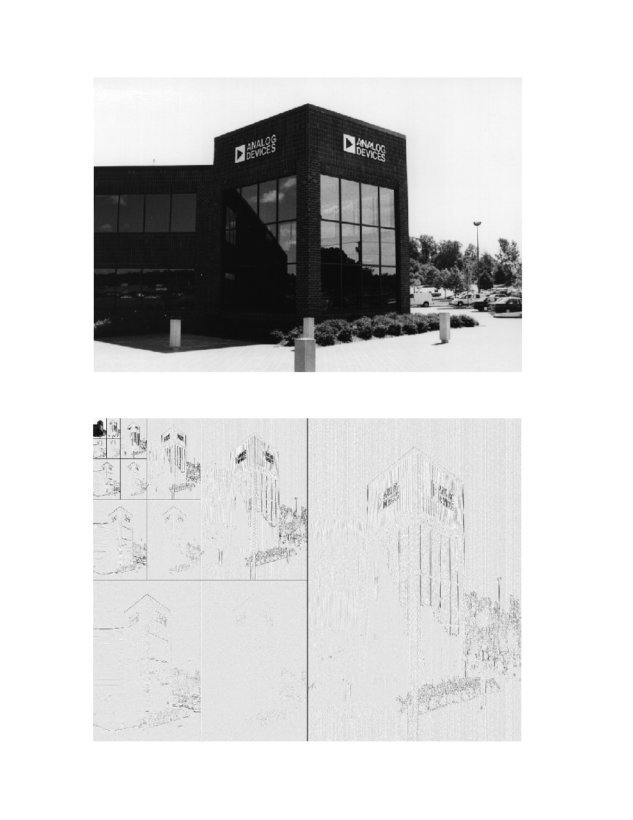
THE WAVELET KERNEL
This block contains a set of filters and decimators that work on
the image in both horizontal and vertical directions. Figure 8
illustrates the filter tree structure. The filters apply carefully
chosen wavelet basis functions that better correlate to the broad-
band nature of images than the sinusoidal waves used in Dis-
crete Cosine Transform (DCT) compression schemes (JPEG,
MPEG, and H261).
An advantage of wavelet-based compression is that the entire
image can be filtered without being broken into sub-blocks as
required in DCT compression schemes. This full image filtering
eliminates the block artifacts seen in DCT compression and
offers more graceful image degradation at high compression
ratios. The availability of full image subband data also makes
image processing, scaling, and a number of other system fea-
tures possible with little or no computational overhead.
The resultant filtered image is made up of components of the
original image as is shown in Figure 5 (a modified Mallat Tree).
Note that Figure 5 shows how a component of video would be
filtered, but in multiple component video, luminance and color
components are filtered separately. In Figure 6 and Figure 7 an
actual image and the Mallat Tree (luminance only) equivalent is
shown. It is important to note that while the image has been
filtered or transformed into the frequency domain, no compres-
sion has occurred. With the image in its filtered state, it is now
ready for processing in the second block, the quantizer.
Understanding the structure and function of the wavelet filters
and resultant product is the key to obtaining the highest perfor-
mance from the ADV611/ADV612. Consider the following
points:
· The data in all blocks (except N) for all components are high
pass filtered. Therefore, the mean pixel value in those blocks
is typically zero and a histogram of the pixel values in these
blocks will contain a single "hump" (Laplacian distribution).
· The data in most blocks is more likely to contain zeros or
strings of zeros than unfiltered image data.
· The human visual system is less sensitive to higher frequency
blocks than low ones.
· Attenuation of the selected blocks in luminance or color com-
ponents results in control over sharpness, brightness, contrast
and saturation.
· High quality filtered/decimated images can be extracted/created
without computational overhead.
Through leverage of these key points, the ADV611/ADV612
not only compresses video, but offers a host of application
features. Please see the Applying the ADV611/ADV612 section
for details on getting the most out of the ADV611/ADV612's
subband coding architecture in different applications.
ADV611/ADV612
6
REV. 0
Figure 6. Unfiltered Original Image (Analog Devices Corporate Offices, Norwood, Massachusetts)
Figure 7. Modified Mallat Diagram of Image
ADV611/ADV612
7
REV. 0
LOW
PASS IN
X
LUMINANCE AND
COLOR
COMPONENTS (EACH
SEPARATELY)
STAGE 1
INDICATES DECIMATE BY TWO IN X
INDICATES DECIMATE BY TWO IN Y
INDICATES
CORRESPONDING
BLOCK LETTER ON
MALLAT DIAGRAM
X 2
BLOCK
A
Y 2
STAGE 2
STAGE 3
STAGE 4
STAGE 5
HIGH
PASS IN
X
X 2
LOW
PASS IN
X
HIGH
PASS IN
X
X 2
X 2
LOW
PASS IN
Y
HIGH
PASS IN
Y
LOW
PASS IN
Y
HIGH
PASS IN
Y
Y 2
Y 2
Y 2
BLOCK
B
BLOCK
C
BLOCK
D
LOW
PASS IN
X
HIGH
PASS IN
X
X 2
X 2
LOW
PASS IN
Y
HIGH
PASS IN
Y
LOW
PASS IN
Y
HIGH
PASS IN
Y
Y 2
Y 2
Y 2
Y 2
BLOCK
#
X 2
Y 2
LOW
PASS IN
X
HIGH
PASS IN
X
BLOCK
E
BLOCK
F
BLOCK
G
X 2
X 2
LOW
PASS IN
Y
HIGH
PASS IN
Y
LOW
PASS IN
Y
HIGH
PASS IN
Y
Y 2
Y 2
Y 2
Y 2
LOW
PASS IN
X
HIGH
PASS IN
X
BLOCK
H
BLOCK
I
BLOCK
J
X 2
X 2
LOW
PASS IN
Y
HIGH
PASS IN
Y
LOW
PASS IN
Y
HIGH
PASS IN
Y
Y 2
Y 2
Y 2
Y 2
BLOCK
K
BLOCK
L
BLOCK
M
BLOCK
N
Figure 8. Wavelet Filter Tree Structure
ADV611/ADV612
8
REV. 0
41
38
35
32
26
23
29
20
17
14
8
5
11
2
Cr COMPONENT
LOW
HIGH
QUANTIZATION OF MALLAT BLOCKS
39
36
33
30
24
21
27
18
15
12
6
3
9
0
Y COMPONENT
40
37
34
31
25
22
28
19
16
13
7
4
10
1
Cb COMPONENT
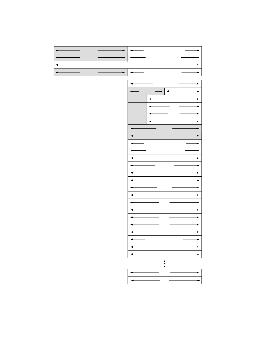
Figure 10. Typical Quantization of Mallat Data Blocks (Graphed)
THE PROGRAMMABLE QUANTIZER
This block quantizes the filtered image based on the response
profile of the human visual system. In general, the human eye
cannot resolve high frequencies in images to the same level of
accuracy as lower frequencies. Through intelligent "quantiza-
tion" of information contained within the filtered image, the
ADV611/ADV612 achieves compression without compromising
the visual quality of the image. Figure 9 shows the encode and
decode data formats used by the quantizer.
Figure 10 shows how a typical quantization pattern applies over
Mallat block data. The high frequency blocks receive much
larger quantization (appear darker) than the low frequency
blocks (appear lighter). Looking at this figure, one sees some key
point concerning quantization: (1) quantization relates directly
to frequency in Mallat block data and (2) levels of quantization
range widely from high to low frequency block. (Note that the
fill is based on a log formula.) The relation between actual
ADV611/ADV612 bin width factors and the Mallat block fill
pattern in Figure 10 appears in Table III.
9.7
WAVELET
DATA
6.10
1/BW
15.17 DATA
0.5
15.0 BIN
NUMBER
QUANTIZER - ENCODE MODE
TRNC
SIGNED
SIGNED
UNSIGNED
1/BW
QUANTIZER - DECODE MODE
8.8 BW
23.8
DE-QUANTIZED
WAVELET DATA
9.7
WAVELET
DATA
15.0 BIN
NUMBER
SIGNED
SIGNED
UNSIGNED
BW
SAT
Figure 9. Programmable Quantizer Data Flow

ADV611/ADV612
9
REV. 0
Table III. Typical Quantization of Mallat Data Block Data
1
Mallat
Bin Width
Reciprocal Bin
Blocks
Factors
Width Factors
39
0x007F
0x0810
40
0x009A
0x06a6
41
0x009A
0x06a6
36
0x00BE
0x0564
33
0x00BE
0x0564
30
0x00E4
0x047e
34
0x00E6
0x0474
35
0x00E6
0x0474
37
0x00E6
0x0474
38
0x00E6
0x0474
31
0x0114
0x03b6
32
0x0114
0x03b6
27
0x0281
0x0199
24
0x0281
0x0199
21
0x0301
0x0155
25
0x0306
0x0153
26
0x0306
0x0153
28
0x0306
0x0153
29
0x0306
0x0153
22
0x03A1
0x011a
23
0x03A1
0x011a
5
0x0A16
0x0066
18
0x0A16
0x0066
12
0x0C1A
0x0055
20
0x0C2E
0x0054
19
0x0C2E
0x0054
17
0x0C2E
0x0054
16
0x0C2E
0x0054
14
0x0E9D
0x0046
13
0x0E9D
0x0046
6
0x1DDC
0x0022
9
0x1DDC
0x0022
3
0x23D5
0x001d
11
0x2410
0x001c
10
0x2410
0x001c
8
0x2410
0x001c
7
0x2410
0x001c
5
0x2B46
0x0018
4
0x2B46
0x0018
0
0xA417
0x0006
2
0xC62B
0x0005
1
0xC62B
0x0005
NOTE
1
The Mallat block numbers, Bin Width factors, and Reciprocal Bin Width
factors in Table III correspond to the shading per-cent fill) of Mallat blocks in
Figure 10.
THE RUN LENGTH CODER AND HUFFMAN CODER
This block contains two types of entropy coders that achieve
mathematically loss-less compression: run-length and Huffman.
The run-length coder looks for long strings of zeros and replaces
them with short hand symbols. Table IV illustrates an example
of how compression is possible.
The Huffman coder is a digital compressor/decompressor that
can be used for compressing any type of digital data. Essentially,
an ideal Huffman coder creates a table of the most commonly
occurring code sequences (typically zero and small values near
zero) and then replaces those codes with some shorthand. The
ADV611/ADV612 employs three fixed Huffman tables; it does
not create tables.
The filters and the quantizer increase the number of zeros and
strings of zeros, which improves the performance of the entropy
coders. The higher the selected compression ratio, the more
zeros and small value sequences the quantizer needs to generate.
The transformed image in Figure 7 shows that the filter bank
concentrates zeros and small values in the higher frequency
blocks.
Encoding vs. Decoding
The decoding of compressed video follows the exact path as
encoding but in reverse order. There is no need to calculate bin
widths during decode because the bin width is stored in the
compressed image during encode.
PROGRAMMER'S MODEL
A host device configures the ADV611/ADV612 using the Host
I/O Port. The host reads from status registers and writes to
control registers through the Host I/O Port.
Table V. Register Description Conventions
Register Name
Register Type (Indirect or Direct, Read or Write) and Address
Register Functional Description Text
Bit [#] or
Bit or Bit Field Name and Usage Description
Bit Range
[High:Low]
0 Action or Indication When Bit Is Cleared (Equals 0)
1 Action or Indication When Bit Is Set (Equals 1)
Table IV. Uncompressed Versus Compressed Data Using Run-Length Coding
0000000000000000000000000000000000000000000000000000000000000000000(uncompressed)
57 Zeros (Compressed)
ADV611/ADV612
10
REV. 0
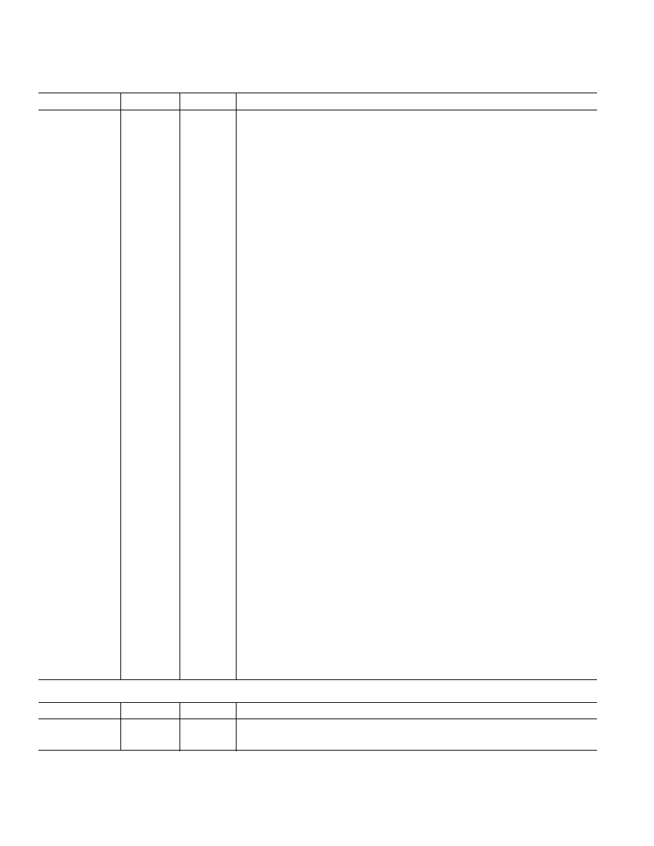
0x100
UNDEF
0x101
UNDEF
0x152
UNDEF
0x153
UNDEF
0x80 0xA9
UNDEF
0xAB
UNDEF
0xAC
UNDEF
0xAD
UNDEF
0xAE
UNDEF
MAX LUMA
0xAA
UNDEF
0xB2
UNDEF
0xB1
UNDEF
0xB0
UNDEF
0xAF
UNDEF
0xB3
0x0
SUM OF SQUARES [0 41]
SUM OF Cb
SUM OF LUMA
SUM OF Cr
MIN LUMA
MAX Cr
MIN Cr
MAX Cb
MIN Cb
RBW0
BW0
RBW41
BW41
INDIRECT REGISTER ADDRESS
RESERVED
RESERVED
0x1
0x88
0x7 0x7F
UNDEF
0x0
0x0980
MODE CONTROL*
0x2
0x000
HSTART
0x3
0x3FF
0x4
0x000
0x5
0x3FF
0x6
UNDEF
0x0
0x4
0x8
0xC
BYTE 3
BYTE 2
BYTE 1
UNDEF
UNDEF
0x00
UNDEF
REGISTER
ADDRESS
DIRECT (EXTERNALLY ACCESSIBLE) REGISTERS
INDIRECT (INTERNALLY INDEXED) REGISTERS
{ACCESS THESE REGISTERS THROUGH THE
INDIRECT REGISTER ADDRESS AND
INDIRECT REGISTER DATA REGISTERS}
*NOTE:
YOU MUST WRITE 0X0880 TO THE MODE
CONTROL REGISTER ON CHIP RESET TO
SELECT THE CORRECT PIXEL MODE
BYTE 0
INDIRECT REGISTER DATA
RESERVED
INTERRUPT MASK / STATUS
RESERVED
COMPRESSED DATA
VSTART
HEND
VEND
FIFO CONTROL
RESERVED
RESERVED
RESET
VALUE
0x8
0xFFFF
COMPRESSED FIELD SIZE LIMIT
0x9
0x7
MODE CONTROL REGISTER 2
COMPRESSED FIELD SIZE HI
0xB4
0x0
COMPRESSED FIELD SIZE LO
Figure 11. Map of ADV611/ADV612 Direct and Indirect Registers

ADV611/ADV612
11
REV. 0
ADV611/ADV612 REGISTER DESCRIPTIONS
Indirect Address Register
Direct (Write) Register Byte Offset 0x00.
This register holds a 16-bit value (index) that selects the indirect register accessible to the host through the indirect data register. All
indirect write registers are 16 bits wide. The address in this register is auto-incremented on each subsequent access of the indirect
data register. This capability enhances I/O performance during modes of operation where the host is calculating Bin Width controls.
[15:0]
Indirect Address Register, IAR[15:0]. Holds a 16-bit value (index) that selects the indirect register to read or write through
the indirect data register (undefined at reset).
[31:16] Reserved (undefined read/write zero)
Indirect Register Data
Direct (Read/Write) Register Byte Offset 0x04
This register holds a 16-bit value read or written from or to the indirect register indexed by the Indirect Address Register.
[15:0]
Indirect Register Data, IRD[15:0]. A 16-bit value read or written to the indexed indirect register. Undefined at reset.
[31:16] Reserved (undefined read/write zero)
Compressed Data Register
Direct (Read/Write) Register Byte Offset 0x08
This register holds a 32-bit sequence from the compressed video bitstream. This register is buffered by a 512 position, 32-bit FIFO.
For Word (16-bit) accesses, access Word0 (Byte 0 and Byte 1) then Word1 (Byte 2 and Byte 3) for correct auto-increment. For a
description of the data sequence, see the Compressed Data Stream Definition section.
[31:0]
Compressed Data Register, CDR[31:0]. 32-bit value containing compressed video stream data. At reset, contents undefined.
Interrupt Mask / Status Register
Direct (Read/Write) Register Byte Offset 0x0C
This 16-bit register contains interrupt mask and status bits that control the state of the ADV611/ADV612's HIRQ pin. With the
seven mask bits (IE_LCODE, IE_STATSR, IE_FIFOSTP, IE_FIFOSRQ, IE_FIFOERR, IE_CCIRER, IE_MERR), select the con-
ditions that are ORed together to determine the output of the HIRQ pin.
Six of the status bits (LCODE, STATSR, FIFOSTP, MERR, FIFOERR, CCIRER) indicate active interrupt conditions and are
sticky bits that stay set until read. Because sticky status bits are cleared when read, and these bits are set on the positive edge of the
condition coming true, they cannot be read or tested for stable level true conditions multiple times.
The FIFOSRQ bit is not sticky. This bit can be polled to monitor for a FIFOSRQ true condition. Note: Enable this monitoring by
using the FIFOSRQ bit and correctly programming DSL and ESL fields within the FIFO control registers.
[0]
CCIR-656 Error in CCIR-656 data stream, CCIRER. This read only status bit indicates the following:
0
No CCIR-656 Error condition, reset value
1
Unrecoverable error in CCIR-656 data stream (missing sync codes)
[1]
Statistics Ready, STATSR. This read only status bit indicates the following:
0
No Statistics Ready condition, reset value (STATS_R pin LO)
1
Statistics Ready for BW calculator (STATS_R pin HI)
[2]
Last Code Read, LCODE. This read only status bit indicates the last compressed data word for field will be
retrieved from the FIFO on the next read from the host bus.
0
No Last Code condition, reset value (LCODE pin LO)
1
Next read retrieves last word for field in FIFO (LCODE pin HI)
[3]
FIFO Service Request, FIFOSRQ. This read only status bit indicates the following:
0
No FIFO Service Request condition, reset value (FIFO_SRQ pin LO)
1
FIFO is nearly full (encode) or nearly empty (decode) (FIFO_SRQ pin HI)
[4]
FIFO Error, FIFOERR. This condition indicates that the host has been unable to keep up with the ADV611/ADV612's
compressed data supply or demand requirements. If this condition occurs during encode, the data stream will not be corrupted
until MERR indicates that the DRAM has also overflowed. If this condition occurs during decode, the video output will be
corrupted. If the system overflows the FIFO (disregarding a FIFOSTP condition) with too many writes in decode mode,
FIFOERR is asserted. This read only status bit indicates the following:
0
No FIFO Error condition, reset value (FIFO_ERR pin LO)
1
FIFO overflow (encode) or underflow (decode) (FIFO_ERR pin HI)

ADV611/ADV612
12
REV. 0
[5]
FIFO Stop, FIFOSTP. This condition indicates that the FIFO is full in decode mode and empty in encode mode. In
decode mode only, FIFOSTP status actually behaves more conservatively than this. In decode mode, even when FIFOSTP
is indicated, there are still 32 empty Dwords available in the FIFO and 32 more Dword writes can safely be performed.
This status bit indicates the following:
0
No FIFO Stop condition, reset value (FIFO_STP pin LO)
1
FIFO empty (encode) or full (decode) (FIFO_STP pin HI)
[6]
Memory Error, MERR. This condition indicates that an error has occurred at the DRAM memory interface. This condition can
be caused by a defective DRAM, the inability of the Host to keep up with the ADV611/ADV612 compressed data stream, or bit
errors in the data stream. Note that the ADV611/ADV612 recovers from this condition without host intervention.
0
No memory error condition, reset value
1
Memory error
[7]
Reserved (always read/write zero)
[8]
Interrupt Enable on CCIRER, IE_CCIRER. This mask bit selects the following:
0
Disable CCIR-656 data error interrupt, reset value
1
Enable interrupt on error in CCIR-656 data
[9]
Interrupt Enable on STATR, IE_STATR. This mask bit selects the following:
0
Disable Statistics Ready interrupt, reset value
1
Enable interrupt on Statistics Ready
[10]
Interrupt Enable on LCODE, IE_LCODE. This mask bit selects the following:
0
Disable Last Code Read interrupt, reset value
1
Enable interrupt on Last Code Read from FIFO
[11]
Interrupt Enable on FIFOSRQ, IE_FIFOSRQ. This mask bit selects the following:
0
Disable FIFO Service Request interrupt, reset value
1
Enable interrupt on FIFO Service Request
[12]
Interrupt Enable on FIFOERR, IE_FIFOERR. This mask bit selects the following:
0
Disable FIFO Stop interrupt, reset value
1
Enable interrupt on FIFO Stop
[13]
Interrupt Enable on FIFOSTP, IE_FIFOSTP. This mask bit selects the following:
0
Disable FIFO Error interrupt, reset value
1
Enable interrupt on FIFO Error
[14]
Interrupt Enable on MERR, IE_MERR. This mask bit selects the following:
0
Disable memory error interrupt, reset value
1
Enable interrupt on memory error
[15]
Reserved (always read/write zero)
Mode Control Register
Indirect (Read/Write) Register Index 0x00
This register holds configuration data for the ADV611/ADV612's video interface format and controls several other video interface
features. For more information on formats and modes, see the Video Interface section. Bits in this register have the following functions:
[3:0]
Video Interface Format, VIF[3:0]. These bits select the interface format. Valid settings include the following (all
other values are reserved):
0x0
CCIR-656, reset value
0x2
MLTPX (Philips)
[4]
VCLK Output Divided by two, VCLK2. This bit controls the following:
0
Do not divide VCLK output (VCLKO = VCLK), reset value
1
Divide VCLK output by two (VCLKO = VCLK/2)
[5]
Video Interface Master/Slave Mode Select, M/S. This bit selects the following:
0
Slave mode video interface (External control of video timing, HSYNC-VSYNC-FIELD are inputs), reset value
1
Master mode video interface (ADV611/ADV612 controls video timing, HSYNC-VSYNC are outputs)
[6]
Video Interface 525/625 (NTSC/PAL) Mode Select, P/N. This bit selects the following:
0
525 mode video interface, reset value
1
625 mode video interface

ADV611/ADV612
13
REV. 0
[7]
Video Interface Encode/Decode Mode Select, E/D. This bit selects the following:
0
Decode mode video interface (compressed-to-raw)
1
Encode mode video interface (raw-to-compressed), reset value
[8]
Reserved (always write zero)
[9]
Video Interface Bipolar/Unipolar Color Component Select, BUC. This bit selects the following:
0
Bipolar color component mode video interface, reset value
1
Unipolar color component mode video interface
[10]
Reserved (always write zero)
[11]
Video Interface Software Reset, SWR. This bit has the following effects on ADV611/ADV612 operations:
0
Normal operation
1
Software Reset. This bit is set on hardware reset and must be cleared before the ADV611/ADV612 can begin processing.
(reset value)
When this bit is set during encode, the ADV611/ADV612 completes processing the current field then suspends operation
until the SWR bit is cleared. When this bit is set during decode, the ADV611/ADV612 suspends operation immediately and
does not resume operation until the SWR bit is cleared. Note that this bit must be set whenever any other bit in the Mode
register is changed.
[12]
HSYNC pin Polarity, PHSYNC. This bit has the following effects on ADV611/ADV612 operations:
0
HSYNC is HI during blanking, reset value
1
HSYNC is LO during blanking (HI during active)
[13]
HIRQ pin Polarity, PHIRQ. This bit has the following effects on ADV611/ADV612 operations:
0
HIRQ is active LO, reset value
1
HIRQ is active HI
[14]
Quality Box Enable, QBE. This bit has the following effect on ADV611/ADV612 operations:
0
Video area registers (HSTART, HEND, VSTART, VEND). Crop video area, setting cropped area to all 0
quantizations (ADV601 mode), reset value
1
Video area registers (HSTART, HEND, VSTART, VEND). Select Quality Box. Quantization of the area outside
the box is selected with the background Contrast Control register. See the video area registers for more information
on the Quality Box.
[15]
Video Stall Enable, VSE. This bit has the following effect on ADV611/ADV612 operations:
0
Video Stall disabled (ADV601 mode), reset value
1
Video Stall enabled.
FIFO Control Register
Indirect (Read/Write) Register Index 0x01
This register holds the service-request settings for the ADV611/ADV612's host interface FIFO, causing interrupts for the "nearly full" and
"nearly empty" levels. Because each register is four bits in size, and the FIFO is 512 positions, the 4-bit value must be multiplied by 32
(decimal) to determine the exact value for encode service level (nearly full) and decode service level (nearly empty). The ADV611/ADV612
uses these settings to determine when to generate a FIFO Service Request related host interrupt (FIFOSRQ bit and FIFO_SRQ pin).
[3:0]
Encode Service Level, ESL[3:0]. The value in this field determines when the FIFO is considered nearly full on encode; a condi-
tion that generates a FIFO service request condition in encode mode. Since this register is four bits (16 states), and the FIFO is
512 positions, the step size for each bit in this register is 32 positions. The following table summarizes sample states of the
register and their meaning.
ESL Interrupt When . . .
0000 Disables service requests (FIFO_SRQ never goes HI during encode)
0001 FIFO has only 32 positions filled (FIFO_SRQ when >= 32 positions are filled)
1000 FIFO is 1/2 full, reset value
1111 FIFO has only 32 positions empty (480 positions filled)
[7:4]
Decode Service Level, DSL[7:4]. The value in this field determines when the FIFO is considered nearly empty in decode; a
condition that generates a FIFO service request in decode mode. Because this register is four bits (16 states), and the FIFO
is 512 positions, the step size for each bit in this register is 32 positions. The following table summarizes sample states of the
register and their meaning.
DSL Interrupt When . . .
0000 Disables service requests (FIFO_SRQ never goes HI)
0001 FIFO has only 32 positions filled (480 positions empty)
1000 FIFO is 1/2 empty, reset value
1111 FIFO has only 32 positions empty (FIFO_SRQ when >= 32 positions are empty)
[15:8]
Reserved (always write zero)

ADV611/ADV612
14
REV. 0
HSTART Register
Indirect (Write Only) Register Index 0x02
This register holds the setting for the horizontal start of the ADV611/ADV612's active video area or quality box. The value in this
register is usually set to zero, but in cases where you wish to crop incoming video it is possible to do so by changing HST.
[9:0]
Horizontal Start, HST[9:0]. 10-bit value defining the start of the active video region. (0 at reset)
[15:10] Reserved (always write zero)
HEND Register
Indirect (Write Only) Register Index 0x03
This register holds the setting for the horizontal end of the ADV611/ADV612's active video area or quality box. If the value is larger
than the max size of the selected video mode, the ADV611/ADV612 uses the max size of the selected mode for HEND.
[9:0]
Horizontal End, HEN[9:0]. 10-bit value defining the end of the active video region. (0x3FF at reset this value is larger
than the max size of the largest video mode)
[15:10] Reserved (always write zero)
VSTART Register
Indirect (Write Only) Register Index 0x04
This register holds the setting for the vertical start of the ADV611/ADV612's active video area or quality box. The value in this
register is usually set to zero unless you want to crop the active video.
To vertically crop video while encoding, program the VSTART and VEND registers with actual video line numbers, which differ for
each field. The VSTART and VEND contents must be updated on each field unless the quality box is enabled. Perform this updating as
part of the field-by-field BW register update process. To perform this dynamic update correctly, the update software must keep track of
which field is being processed next.
[9:0]
Vertical Start, VST[9:0]. 10-bit value defining the starting line of the active video region, with line numbers from 1-to-625
in PAL and 1-to-525 in NTSC. (0 at reset)
[15:10] Reserved (always write zero)
VEND Register
Indirect (Write Only) Register Index 0x05
This register holds the setting for the vertical end of the ADV611/ADV612's active video area or quality box. If the value is larger
than the max size of the selected video mode, the ADV611/ADV612 uses the max size of the selected mode for VEND.
VIDEO AREA REGISTERS
When the quality box is disabled (Mode Control register, Bit 14 = 0), the area defined by the HSTART, HEND, VSTART and
VEND registers is the active area that the wavelet kernel processes. Video data outside the active video area is set to minimum lumi-
nance and zero chrominance (black) by the ADV611/ADV612. These registers allow cropping of the input video during compression
(encode only), but do not change the image size. Figure 12 shows how the video area registers work together.
Some comments on how these registers work are as follows:
· The vertical numbers include the blanking areas of the video.
Specifically, a VSTART value of 21 will include the first line
of active video, and the first pixel in a line corresponds to a
value HSTART of 0 (for NTSC regular).
Note that the vertical coordinates start with 1, whereas the
horizontal coordinates start with 0.
· The default cropping mode is set for the entire frame. Specifi-
cally, Field 2 starts at a VSTART value of 283 (for NTSC
regular).
When the quality box is enabled (Mode Control register, Bit 14
= 1), the area defined by the HSTART, HEND, VSTART and
VEND registers is the quality box area, and the rest of the video
area is attenuated according to the value in the background
Contrast Control register (Indirect Register Index 0x9). In this
mode, the range of values for VSTART and VEND is 1243 for
NTSC and 1288 for PAL. Also note that VSTART and VEND
do not need to be updated for each field in this mode.
VSTART
VEND
HSTART
HEND
ZERO
ZERO
ZERO
X, Y
ACTIVE VIDEO AREA
0, 0
ZERO
ZERO
ZERO
ZERO
ZERO
MAX FOR SELECTED VIDEO MODE
Figure 12. Video Area and Video Area Registers

ADV611/ADV612
15
REV. 0
To vertically crop video while encoding, program the VSTART and VEND registers with actual video line numbers, which differ for each
field. The VSTART and VEND contents must be updated on each field, unless the quality box is enabled. Perform this updating as part of
the field-by-field BW register update process. To perform this dynamic update correctly, the update software must keep track of which
field is being processed next.
[9:0]
Vertical End, VEN[9:0]. 10-bit value defining the ending line of the active video region, with line numbers from 1-to-625
in PAL and 1-to-525 in NTSC. (0x3FF at reset--this value is larger than the max size of the largest video mode)
[15:10] Reserved (always write zero)
Compressed Field Size Limit
Indirect (Read/Write) Register Index 0x8
[15:0]
The DWORD Max Count 16 MSBs register selects the maximum number of double (32-bit) words for an encoded field.
When the value in the DWORD count registers reaches the DWORD Max Count, the Quantizer zeroes out all remaining
samples in the field. To enable the DWORD Max Counts operation, you must set (= 1) Bit 4 in Indirect register 0x7; all
other bits in Indirect register 0x7 are reserved ( = 0). Note that the 4 LSBs of the max count are 0000, so the max count is
selectable in 16-word increments. Contains bits [19:4] of the DWORD max count, reset to 0xffff
Mode Control #2
Indirect (Read/Write) Register Index 0x9
[2:0]
These bits control the contrast/attenuation of the area outside the quality box when the quality box is enabled. The
following settings control background contrast.
Setting
Contrast/Attenuation
000
Illegal
001
6 dB
010
12 dB
011
18 dB
100
24 dB
101
30 dB
[3]
Field Polarity Bit. This bit reverses the polarity of the FIELD pin. This bit operates as follows:
0
Normal Field Polarity (ADV601 Mode), reset value
1
Reverse Field Polarity. Polarity is opposite to the polarity in the FIELD pin timing diagrams.
[8:4]
Field Rate Reduction. To reduce this compressed data rate, the ADV601 can discard some video fields. Set field rate
reduction to zero to capture all fields, one to discard every other field, two to discard two fields out of three and so on.
Maximum possible field rate reduction send only one field out of 32.
[9]
Reserved, must set to 1. This bit must be set to take advantage of MERR detection logic. Resets to 0.
[10]
Reserved, resets to 1.
[11]
Ignore Field bit in decode, setting this bit eliminates black fields if field bits repeat from field to field in decode mode,
resets to 0.
Sum of Squares [041] Registers
Indirect (Read Only) Register Index 0x080 through 0x0A9
The Sum of Squares [041] registers hold values that correspond to the summation of squared values in corresponding Mallat blocks
[041]. These registers let the Host or DSP read sum of squares statistics from the ADV611/ADV612; using these values (with the
Sum of Value, MIN Value, and MAX Value) the host or DSP can then calculate the BW and RBW values. The ADV611/ADV612
indicates that the sum of squares statistics have been updated by setting (1) the STATR bit and asserting the STAT_R pin. Read the
statistics at any time. The Host reads these values through the Host Interface.
[15:0]
Sum of Squares, STS[15:0]. 16-bit values [0-41] for corresponding Mallat blocks [0-41] (undefined at reset). Sum of Square
values are 16-bit codes that represent the Most Significant Bits of values ranging from 40 bits for small blocks to 48 bits for
large blocks. The 16-bit codes have the following precision:
Blocks Precision
Sum of Squares Precision Description
02
48.32
48.-bits wide, left shift code by 32-bits, and zero fill
311
46.30
46.-bits wide, left shift code by 30-bits, and zero fill
1220
44.28
44.-bits wide, left shift code by 28-bits, and zero fill
2129
42.26
42.-bits wide, left shift code by 26-bits, and zero fill
3041
40.24
40.-bits wide, left shift code by 24-bits, and zero fill
If the Sum of Squares code were 0x0025 for block 10, the actual value would be 0x000940000000; if using that same
code, 0x0025, for block 30, the actual value would be 0x0025000000.
[31:0]
Reserved (always read zero)

ADV611/ADV612
16
REV. 0
Sum of Luma Value Register
Indirect (Read Only) Register Index 0x0AA
The Sum of Luma Value register lets the host or DSP read the sum of pixel values for the Luma component in block 39. The
Host reads these values through the Host Interface.
[15:0]
Sum of Luma, SL[15:0]. 16-bit component pixel values (undefined at reset)
[31:0]
Reserved (always read zero)
Sum of Cb Value Register
Indirect (Read Only) Register Index 0x0AB
The Sum of Cb Value register lets the host or DSP read the sum of pixel values for the Cb component in block 40. The Host
reads these values through the Host Interface.
[15:0]
Sum of Cb, SCB[15:0]. 16-bit component pixel values (undefined at reset)
[31:0]
Reserved (always read zero)
Sum of Cr Value Register
Indirect (Read Only) Register Index 0x0AC
The Sum of Cr Value register lets the host or DSP read the sum of pixel values for the Cr component in block 41. The Host
reads these values through the Host Interface.
[15:0]
Sum of Cr, SCR[15:0]. 16-bit component pixel values (undefined at reset)
[31:0]
Reserved (always read zero)
MIN Luma Value Register
Indirect (Read Only) Register Index 0x0AD
The MIN Luma Value register lets the host or DSP read the minimum pixel value for the Luma component in the unprocessed
data. The Host reads these values through the Host Interface.
[15:0]
Minimum Luma, MNL[15:0]. 16-bit component pixel value (undefined at reset)
[31:0]
Reserved (always read zero)
MAX Luma Value Register
Indirect (Read Only) Register Index 0x0AE
The MAX Luma Value register lets the host or DSP read the maximum pixel value for the Luma component in the unprocessed
data. The Host reads these values through the Host Interface.
[15:0]
Maximum Luma, MXL[15:0]. 16-bit component pixel value (undefined at reset)
[31:0]
Reserved (always read zero)
MIN Cb Value Register
Indirect (Read Only) Register Index 0x0AF
The MIN Cb Value register lets the host or DSP read the minimum pixel value for the Cb component in the unprocessed data.
The Host reads these values through the Host Interface.
[15:0]
Minimum Cb, MNCB[15:0], 16-bit component pixel value (undefined at reset)
[31:0]
Reserved (always read zero)
MAX Cb Value Register
Indirect (Read Only) Register Index 0x0B0
The MAX Cb Value register lets the host or DSP read the maximum pixel value for the Cb component in the unprocessed data.
The Host reads these values through the Host Interface.
[15:0]
Maximum Cb, MXCB[15:0].16-bit component pixel value (undefined at reset)
[31:0]
Reserved (always read zero)

ADV611/ADV612
17
REV. 0
MIN Cr Value Register
Indirect (Read Only) Register Index 0x0B1
The MIN Cr Value register lets the host or DSP read the minimum pixel value for the Cr component in the unprocessed data. The
Host reads these values through the Host Interface.
[15:0]
Minimum Cr, MNCR[15:0]. 16-bit component pixel value (undefined at reset)
[31:0]
Reserved (always read zero)
MAX Cr Value Register
Indirect (Read Only) Register Index 0x0B2
The MAX Cr Value register lets the host or DSP read the maximum pixel value for the Cr component in the unprocessed data. The
Host reads these values through the Host Interface.
[15:0]
Maximum Cr, MXCR[15:0]. 16-bit component pixel value (undefined at reset)
[31:0]
Reserved (always read zero)
Compressed Field Size [HI]
Indirect (Read Only) Register Index 0x83
[15:0]
The DWORD Count registers hold the count of double (32-bit) words contained in the previously encoded field. This
count is useful for bit rate control algorithms that use a servo loop, which is locked to the expected number of double words
in the field. The registers are double buffered to ensure that the count remains constant while the next field's count accumu-
lates. Contains bits [19:4] of the DWORD count, reset is 0.
Compressed Field Size [LO]
Indirect (Read Only) Register Index 0xB4
[3:0]
Contains bits [3:0] of the DWORD count, reset is 0. For more information, see the DWORD Count 16 MSB Register
description.
Bin Width and Reciprocal Bin Width Registers
Indirect (Read/Write) Register Index 0x0100-0x0153
The RBW and BW values are calculated by the host or DSP from data in the Sum of Squares [0-41], Sum of Value, MIN Value, and
MAX Value registers; then are written to RBW and BW registers during encode mode to control the quantizer. The Host writes these
values through the Host Interface.
These registers contain a 16-bit interleaved table of alternating RBW/BW (RBW-even addresses and BW-odd addresses) values as
indexed on writes by address register. Bin Widths are 8.8, unsigned, 16-bit, fixed-point values. Reciprocal Bin Widths are 6.10, un-
signed, 16-bit, fixed-point values. Operation of this register is controlled by the host driver or the DSP (84 total entries) (undefined
at reset).
[15:0]
Bin Width Values, BW[15:0]
[15:0]
Reciprocal Bin Width Values, RBW[15:0]

ADV611/ADV612
18
REV. 0
PIN FUNCTION DESCRIPTIONS
Clock Pins
Name
Pins
I/O
Description
VCLK/XTAL
2
I
A single clock (VCLK) or crystal input (across VCLK and XTAL). An acceptable
50% duty cycle clock signal is 27 MHz (CCIR-601 NTSC/PAL).
If using a clock crystal, use a parallel resonant, microprocessor grade clock crystal. If
using a clock input, use a TTL level input, 50% duty cycle clock with 1 ns (or less)
jitter (measured rising edge to rising edge). Slowly varying, low jitter clocks are
acceptable; up to 5% frequency variation in 0.5 sec.
VCLKO
1
O
VCLK Output or VCLK Output divided by two. Select function using Mode
Control register.
Video Interface Pins
Name
Pins
I/O
Description
VSYNC
1
I or O
Vertical Sync or Vertical Blank. This pin can be either an output (Master Mode) or
an input (Slave Mode). The pin operates as follows:
·
Output (Master) HI during inactive lines of video and LO otherwise
·
Input (Slave) a HI on this input indicates inactive lines of video
HSYNC
1
I or O
Horizontal Sync or Horizontal Blank. This pin can be either an output (Master
Mode) or an input (Slave Mode). The pin operates as follows:
·
Output (Master) HI during inactive portion of video line and LO otherwise
·
Input (Slave) a HI on this input indicates inactive portion of video line
Note that the polarity of this signal is modified using the Mode Control register. For
detailed timing information, see the Video Interface section.
FIELD
1
I or O
Field # or Frame Sync. Polarity of FIELD Pin can be reversed by setting Bit 3 in
Mode Control Register 2. The pin operates as follows:
·
Output (Master) HI during Field1 lines of video and LO otherwise
·
Input (Slave) a HI on this input indicates Field1 lines of video
ENC
1
O
Encode or Decode. This output pin indicates the coding mode of the ADV611/
ADV612 and operates as follows:
·
LO Decode Mode (Video Interface is output)
·
HI Encode Mode (Video Interface is input)
Note that this pin can be used to control bus enable pins for devices connected to
the ADV611/ADV612 Video Interface.
VDATA[7:0]
8
I/O
4:2:2 Video Data (8-bit digital component video data). These pins are inputs during
encode mode and outputs during decode mode. When outputs (decode) these pins
are compatible with 50 pF loads (rather than 30 pF as all other busses) to meet the
high performance and large number of typical loads on this bus.
The performance of these pins varies with the Video Interface Mode set in the
Mode Control register, see the Video Interface section of this data sheet for pin
assignments in each mode.
Note that the Mode Control register also sets whether the color component is
treated as either signed or unsigned.
STALL
1
I
Stall Mode. This pin stalls incoming video data driving encode.

ADV611/ADV612
19
REV. 0
DRAM Interface Pins
Name
Pins
I/O
Description
DDAT[15:0]
16
I/O
DRAM Data Bus. The ADV611/ADV612 uses these pins for 16-bit data read/
write operations to the external 256K
×
16-bit DRAM. (The operation of the
DRAM interface is fully automatic and controlled by internal functionality
of the ADV611/ADV612.) These pins are compatible with 30 pF loads.
DADR[8:0]
9
O
DRAM Address Bus. The ADV611/ADV612 uses these pins to form the multi-
plexed row/column address lines to the external DRAM. (The operation of the
DRAM interface is fully automatic and controlled by internal functionality
of the ADV611/ADV612.) These pins are compatible with 30 pF loads.
RAS
1
O
DRAM Row Address Strobe. This pin is compatible with 30 pF loads.
CAS
1
O
DRAM Column Address Strobe. This pin is compatible with 30 pF loads.
WE
1
O
DRAM Write Enable. This pin is compatible with 30 pF loads.
Note that the ADV611/ADV612 does not have a DRAM OE pin. Tie the
DRAM's OE pin to ground.
Host Interface Pins
Name
Pins
I/O
Description
DATA[31:0]
32
I/O
Host Data Bus. These pins make up a 32-bit wide host data bus. The host
controls this asynchronous bus with the WR, RD, BE and CS pins to commu-
nicate with the ADV611/ADV612. These pins are compatible with 30 pF loads.
ADR[1:0]
2
I
Host DWord Address Bus. These two address pins let you address the
ADV611/ADV612's four directly addressable host interface registers. For an
illustration of how this addressing works, see the Control and Write Register
Map figure and Status and Read Register Map figure. The ADR bits permit
register addressing as follows:
ADR1
ADR0
DWord
Address Byte Address
0
0
0
0x00
0
1
1
0x04
1
0
2
0x08
1
1
3
0x0C
BE0BE1
2
I
Host Word Enable pins. These two input pins select the words that the ADV611/
BE2BE3
ADV612's direct and indirect registers access through the Host Interface;
BE0BE1 access the least significant word, and BE2BE3 access the most
significant word. For a 32-bit interface only, tie these pins to ground, making
all words available.
Some important notes for 16-bit interfaces are as follows:
·
When using these byte enable pins, the byte order is always the lowest byte
·
to the higher bytes.
·
The ADV611/ADV612 advances to the next 32-bit compressed data FIFO
·
location after the BE2BE3 pin is asserted then de-asserted (when accessing the
·
Compressed Data register); so the FIFO location only advances when and if
·
the host reads or writes the MSW of a FIFO location.
·
The ADV611/ADV612 advances to the next 16-bit indirect register after the
·
BE0BE1 pin is asserted then de-asserted; so the register selection only advances
·
when and if the host reads or writes the MSW of a 16-bit indirect register.
CS
1
I
Host Chip Select. This pin operates as follows:
·
LO Qualifies Host Interface control signals
·
HI Three-states DATA[31:0] pins
WR
1
I
Host Write. Host register writes occur on the rising edge of this signal.
RD
1
I
Host Read. Host register reads occur on the low true level of this signal.
ADV611/ADV612
20
REV. 0
Host Interface Pins
(Continued)
Name
Pins
I/O
Description
ACK
1
O
Host Acknowledge. The ADV611/ADV612 acknowledges completion of a Host
Interface access by asserting this pin. Most Host Interface accesses (other than the
compressed data register access) result in ACK being held high for at least one wait
cycle, but some exceptions to that rule are as follows:
·
A full FIFO during decode operations causes the ADV611/ADV612 to de-assert
·
(drive HI) the ACK pin, holding off further writes of compressed data until
·
the FIFO has one available location.
·
An empty FIFO during encode operations causes the ADV611/ADV612 to de-
·
assert (drive HI) the ACK pin, holding off further reads until one location is filled.
FIFO_SRQ
1
O
FIFO Service Request. This pin is an active high signal indicating that the FIFO
needs to be serviced by the host. (see FIFO Control register). The state of this pin
also appears in the Interrupt Mask/Status register. Use the interrupt mask to assert a
Host interrupt (HIRQ pin) based on the state of the FIFO_SRQ pin. This pin oper-
ates as follows:
·
LO No FIFO Service Request condition (FIFOSRQ bit LO)
·
HI FIFO needs service is nearly full (encode) or nearly empty (decode)
During encode, FIFO_SRQ is LO when the SWR bit is cleared (0) and goes HI
when the FIFO is nearly full (see FIFO Control register).
During decode, FIFO_SRQ is HI when the SWR bit is cleared (0), because FIFO
is empty, and goes LO when the FIFO is filled beyond the nearly empty condition
(see FIFO Control register).
STATS_R
1
O
Statistics Ready. This pin indicates the Wavelet Statistics (contents of Sum of
Squares, Sum of Value, MIN Value, MAX Value registers) have been updated and
are ready for the Bin Width calculator to read them from the host interface. The
frequency of this interrupt will be equal to the field rate. The state of this pin also
appears in the Interrupt Mask/Status register. Use the interrupt mask to assert a
Host interrupt (HIRQ pin) based on the state of the STATS_R pin. This pin oper-
ates as follows:
·
LO No Statistics Ready condition (STATSR bit LO)
·
HI Statistics Ready for BW calculator (STATSR bit HI)
LCODE
1
O
Last Compressed Data (for field). This bit indicates the last compressed data word
for field will be retrieved from the FIFO on the next read from the host bus. The
frequency of this interrupt is similar to the field rate, but varies depending on
compression and host response. The state of this pin also appears in the Interrupt
Mask/Status register. Use the interrupt mask to assert a Host interrupt (HIRQ pin)
based on the state of the LCODE pin. This pin operates as follows:
·
LO No Last Code condition (LCODE bit LO)
·
HI Last data word for field has been read from FIFO (LCODE bit HI)
HIRQ
1
O
Host Interrupt Request. This pin indicates an interrupt request to the Host. The
Interrupt Mask/Status register can select conditions for this interrupt based on any
or all of the following: FIFOSTP, FIFOSRQ, FIFOERR, LCODE, STATR or
CCIR-656 unrecoverable error. Note that the polarity of the HIRQ pin can be
modified using the Mode Control register.
RESET
1
I
ADV611/ADV612 Chip Reset. Asserting this pin returns all registers to reset state.
Note that the ADV611/ADV612 must be reset at least once after power-up with this
active low signal input. For more information on reset, see the SWR bit description.
Power Supply Pins
Name
Pins
I/O
Description
GND
16
I
Ground
VDD
13
I
+5 V dc Digital Power

ADV611/ADV612
21
REV. 0
Video Interface
The ADV611/ADV612 video interface supports two types of
component digital video (D1) interfaces in both compression
(input) and decompression (output) modes. These digital video
interfaces include support for the Multiplexed Philips 4:2:2 and
CCIR-656/SMPTE125M--international standard.
Video interface master and slave modes allow for the generation or
receiving of synchronization and blanking signals. Definitions for
the different formats can be found later in this section. For recom-
mended connections to popular video decoders and encoders, see
the Connecting the ADV611/ADV612 to Popular Video Decoders
and Encoders section. A complete list of supported video interfaces
and sampling rates is included in Table VI.
Table VI. Component Digital Video Interfaces
Nominal
Bits/
Color
Date
Name
Component
Space
Sampling
Rate (MHz) I/F Width
CCIR-656
8
YCrCb
4:2:2
27
8
Multiplex
Philips
8
YUV
4:2:2
27
8
Internally, the video interface translates all video formats to one
consistent format to be passed to the wavelet kernel. This con-
sistent internal video standard is 4:2:2 at 16 bits accuracy.
VITC and Closed Captioning Support
The video interface also supports the direct loss-less extraction
of 90-bit VITC codes during encode and the insertion of VITC
codes during decode. Closed Captioning data (found on active
Video Line 21) is handled just as normal active video on an
active scan line. As a result, no special dedicated support is
necessary for Closed Captioning. The data rates for Closed
Captioning data are low enough to ensure robust operation of
this mechanism at compression ratios of 50:1 and higher. Note
that you must include Video Line 21 in the ADV611/ADV612's
defined active video area for Closed Caption support.
27 MHz Nominal Sampling
There is one clock input (VCLK) to support all internal process-
ing elements. This is a 50% duty cycle signal and must be syn-
chronous to the video data. Internally this clock is doubled using
a phase locked loop to provide for a 54 MHz internal processing
clock. The clock interface is a two pin interface that allows a
crystal oscillator to be tied across the pins or a clock oscillator to
drive one pin. The nominal clock rate for the video interface is
27 MHz. Note that the ADV611/ADV612 also supports a pixel
rate of 13.5 MHz.
Video Interface and Modes
In all, there are seven programmable features that configure the
video interface. These are:
· Encode-Decode Control
In addition to determining what functions the internal pro-
cessing elements must perform, this control determines the
direction of the video interface. In decode mode, the video
interface outputs data. In encode mode, the interface receives
data. The state of the control is reflected on the ENC pin.
This pin can be used as an enable input by external line driv-
ers. This control is maintained by the host processor.
· Master-Slave Control
This control determines whether the ADV611/ADV612 gen-
erates or receives the VSYNC, HSYNC, and FIELD signals.
In master mode, the ADV611/ADV612 generates these sig-
nals for external hardware synchronization. In slave mode, the
ADV611/ADV612 receives these signals. Note that some video
formats require the ADV611/ADV612 to operate in slave mode
only. This control is maintained by the host processor.
· 525-625 (NTSC-PAL) Control
This control determines whether the ADV611/ADV612 is
operating on 525/NTSC video or 625/PAL video. This infor-
mation is used when the ADV611/ADV612 is in master and
decode modes so that the ADV611/ADV612 knows where
and when to generate the HSYNC, VSYNC, and FIELD
Pulses as well as when to insert the SAV and EAV time codes
(for CCIR-656 only) in the data stream. This control is main-
tained by the host processor. Table VII shows how the 525-
625 Control in the Mode Control register works.
Table VII. Square Pixel Control, 525-625 Control, and
Video Formats
Max
Max
525-625
Horizontal
Field
Control
Size
Size
NTSC-PAL
0
720
243
CCIR-601 NTSC
1
720
288
CCIR-601 PAL
· Bipolar/Unipolar Color Component
This mode determines whether offsets are used on color com-
ponents. In Philips mode, this control is usually set to Bipo-
lar, since the color components are normal twos-compliment
signed values. In CCIR-656 mode, this control is set to Uni-
polar, since the color components are offset by 128. Note that
it is likely the ADV611/ADV612 will function if this control is
in the wrong state, but compression performance will be
degraded. It is important to set this bit correctly.
· Active Area Control
Four registers HSTART (horizontal start), HEND (horizon-
tal end), VSTART (vertical start) and VEND (vertical end)
determine the active video area. The maximum active video
area is 720 by 288 pixels for a single field.
· Video Format
This control determines the video format that is supported. In
general, the goal of the various video formats is to support
glueless interfaces to the wide variety of video formats periph-
eral components expect. This control is maintained by the
host processor. Table VIII shows a synopsis of the supported
video formats. Definitions of each format can be found later
in this section. For Video Interface pins descriptions, see the
Pin Function Descriptions.

ADV611/ADV612
22
REV. 0
Table IX. CCIR-656 Master and Slave Modes HSYNC, VSYNC, and FIELD Functionality
HSYNC, VSYNC and FIELD
Master Mode (HSYNC, VSYNC
Slave Mode (HSYNC, VSYNC
Functionality for CCIR-656
and FIELD Are Outputs)
and FIELD Are Inputs)
Encode Mode (video data is input
Pins are driven to reflect the states of the
These pins are used to control the
to the chip)
received time codes: EAV and SAV. This
blanking of video and sequencing (used
functionality is independent of the state of
with video decoders that do not con-
the 525-625 mode control. An encoder is
form to the correct number of samples
most likely to be in master mode.
per line [e.g., the Harris 8115]).
Decode Mode (video data is output
Pins are output to the precise timing definitions
Undefined--Use Master Mode
from the chip)
for CCIR-656 interfaces. The state of the pins
reflect the state of the EAV and SAV timing
codes that are generated in the output video data.
These definitions are different for 525 and 625 line
systems. The ADV611/ADV612 completely manages
the generation and timing of these pins.
Clocks and Strobes
All video data is synchronous to the video clock (VCLK).
The rising edge of VCLK is used to clock all data into the
ADV611/ADV612.
Synchronization and Blanking Pins
Three signals, which can be configured as inputs or outputs, are
used for video frame and field horizontal synchronization and
blanking. These signals are VSYNC, HSYNC, and FIELD.
VDATA Pins Functions With Differing Video Interface Formats
The functionality of the Video Interface pins depends on the
current video format.
Video Formats--CCIR-656
The ADV611/ADV612 supports a glueless video interface to
CCIR-656 devices when the Video Format is programmed to
CCIR-656 mode. CCIR-656 requires that 4:2:2 data (8 bits per
component) be multiplexed and transmitted over a single 8-bit
physical interface. A 27 MHz clock is transmitted along with the
data. This clock is synchronous with the data. The color space of
CCIR-656 is YCrCb.
When in master mode, the CCIR-656 mode does not require
any external synchronization or blanking signals to accompany
digital video. Instead, CCIR-656 includes special time codes
in the stream syntax that define horizontal blanking periods,
Table VIII. Component Digital Video Formats
Nominal
Bit/
Color
Data Rate
Master/
Format
Name
Component
Space
Sampling
(MHz)
Slave
I/F Width
Number
CCIR-656
8
YCrCb
4:2:2
27
Master
8
0x0
Multiplex Philips
8
YUV
4:2:2
27
Either
8
0x2
vertical blanking periods, and field synchronization (horizontal
and vertical synchronization information can be derived). These
time codes are called End-of-Active-Video (EAV) and Start-of-
Active-Video (SAV). Each line of video has one EAV and one
SAV time code. EAV and SAV have three bits of embedded
information to define HSYNC, VSYNC and Field information
as well as error detection and correction bits.
VCLK is driven with a 27 MHz, 50% duty cycle clock which is
synchronous with the video data. Video data is clocked on the
rising edge of the VCLK signal. When decoding, the VCLK
signal is typically transmitted along with video data in the
CCIR-656 physical interface.
Electrically, CCIR-656 specifies differential ECL levels to be
used for all interfaces. The ADV611/ADV612, however, only
supports unipolar, TTL logic thresholds. Systems designs that
interface to strictly conforming CCIR-656 devices (especially
when interfacing over long cable distances) must include ECL
level shifters and line drivers.
The functionality of HSYNC, VSYNC and FIELD Pins is
dependent on three programmable modes of the ADV611/
ADV612: Master-Slave Control, Encode-Decode Control and
525-625 Control. Table X summarizes the functionality of
these pins in various modes.
ADV611/ADV612
23
REV. 0
Video Formats--References
For more information on video interface standards, see the
following reference texts.
· For the definition of CCIR-601:
1992 CCIR Recommendations RBT series Broadcasting Service
(Television) Rec. 601-3 Encoding Parameters of digital television
for studios, page 35, September 15, 1992.
· For the definition of CCIR-656:
1992 CCIR Recommendations RBT series Broadcasting Service
(Television) Rec. 656-1 Interfaces for digital component video
signals in 525 and 626 line television systems operating at the
4:2:2 level of Rec. 601, page 46, September 15, 1992.
Host Interface
The ADV611/ADV612 host interface is a high performance
interface that passes all command and real-time compressed
video data between the host and codec. A 512 position by 32-bit
wide, bidirectional FIFO buffer passes compressed video data
to and from the host. The host interface is capable of burst
transfer rates of up to 132 million bytes per second (4
×
33 MHz).
For host interface pins descriptions, see the Pin Function De-
scriptions section. For host interface timing information, see the
Host Interface Timing section.
Video Formats -- Multiplexed Philips Video
The ADV611/ADV612 supports a hybrid mode of operation that
is a cross between standard dual lane Philips and single lane
CCIR-656. In this mode, video data is multiplexed in the same
fashion in CCIR-656, but the values 0 and 255 are not reserved as
signaling values. Instead, external HSYNC and VSYNC pins are
used for signaling and video synchronization. VCLK may range
up to 27 MHz.
VCLK is driven with up to a 27 MHz 50% duty cycle clock
synchronous with the video data. Video data is clocked on the
rising edge of the VCLK signal. The functionality of HSYNC,
VSYNC, and FIELD pins is dependent on three programmable
modes of the ADV611/ADV612; Master-Slave Control, Encode-
Decode Control, and 525-625 Control. Table IX summarizes
the functionality of these pins in various modes.
Table X. Philips Multiplexed Video Master and Slave Modes HSYNC, VSYNC, and FIELD Functionality
HSYNC, VSYNC and FIELD
Functionality for Multiplexed
Master Mode (HSYNC, VSYNC
Slave Mode (HSYNC, VSYNC
Philips
and FIELD Are Outputs)
and FIELD Are Inputs)
Encode Mode (video data is input
The ADV611/ADV612 completely manages the generation
These pins are used to control the
to the chip)
and timingof these pins. The device driving the ADV611/ blanking of video and sequencing.
ADV612 video interface must use these outputs to remain
in sync with the ADV611/ADV612. It is expected that this
combination of modes would not be used frequently.
Decode Mode (video data is output The ADV611/ADV612 completely manages the generation These pins are used to control the
from the chip)
and timing of these pins.
blanking of video and sequencing.
DRAM Manager
The DRAM Manager provides a sorting and reordering func-
tion on the subband coded data between the Wavelet Kernel
and the Programmable Quantizer. The DRAM manager pro-
vides a pipeline delay stage to the ADV611/ADV612. This
pipeline lets the ADV611/ADV612 extract current field image
statistics (min/max pixel values, sum of pixel values, and sum of
squares) used in the calculation of bin widths and reorder
wavelet transform data. The use of current field statistics in the
bin width calculation results in precise control over the com-
pressed bit rate. The DRAM manager manages the entire opera-
tion and refresh of the DRAM.
The interface between the ADV611/ADV612 DRAM man-
ager and DRAM is designed to be transparent to the user. The
ADV611/ADV612 DRAM pins should be connected to the
DRAM as called out in the Pin Function Descriptions section.
The ADV611/ADV612 requires one 256K word by 16-bit,
60 ns DRAM. The following is a selected list of manufacturers
and part numbers. All parts can be used with the ADV611/
ADV612 at all VCLK. Any DRAM used with the ADV611/
ADV612 must meet the minimum specifications outlined for
the Hyper Mode DRAMs listed in Table XI. For DRAM Inter-
face pins descriptions, see the Pin Function Descriptions.
Table XI. Compatible DRAMs
Manufacturer
Part Number
Notes
Toshiba
TC514265DJ/DZ/DFT-60
None
NEC
µ
PD424210ALE-60
None
NEC
µ
PD42S4210ALE-60
CBR Self-Refresh
feature of this
product is not
needed by the
ADV611/ADV612.
Hitachi
HM514265CJ-60
None
ADV611/ADV612
24
REV. 0
(CONTINUOUS STREAM OF FRAMES)
TIME
FRAME (N)
FRAME (N + 1)
FRAME (N + 2)
FRAME (N + M)
FIELD 2 SEQUENCE
FIELD 1 SEQUENCE
FIELD SEQUENCE STRUCTURE
FIRST BLOCK SEQUENCE
COMPLETE BLOCK SEQUENCE
VERTICAL INTERFACE TIME CODE
FIRST BLOCK SEQUENCE STRUCTURE
DATA FOR MALLAT BLOCK 6
BIN WIDTH QUANTIZER CODE
SUB-BAND TYPE CODE
COMPLETE BLOCK SEQUENCE ORDER
(STREAM OF MALLAT
BLOCK SEQUENCES)
SEQUENCE FOR MALLAT BLOCK 3
SEQUENCE FOR MALLAT BLOCK 20
SEQUENCE FOR MALLAT BLOCK 9
COMPLETE BLOCK (INDIVIDUAL) SEQUENCE STRUCTURE
DATA FOR MALLAT BLOCK
BIN WIDTH QUANTIZER CODE
START OF BLOCK CODE
START OF FIELD 1 OR 2 CODE
Figure 13. Hierarchical Structure of Wavelet Compressed Frame Data (Data Block Order)
Compressed Data-Stream Definition
Through its Host Interface the ADV611/ADV612 outputs (dur-
ing encode) and receives (during decode) compressed digital
video data. This stream of data passing between the ADV611/
ADV612 and the host is hierarchically structured and broken up
into blocks of data as shown in Figure 13. Table V shows
pseudo code for a video data transfer that matches the transfer
order shown in Figure 13 and uses the code names shown in
Table XIV. The blocks of data listed in Figure 13 correspond to
wavelet compressed sections of each field illustrated in Figure 13
as a modified Mallat diagram.

ADV611/ADV612
25
REV. 0
Table XII. Pseudo-Code Describing a Sequence of Video Fields
Complete Sequence:
<Field 1 Sequence>
"Frame N; Field 1"
<Field 2 Sequence>
"Frame N; Field 2"
<Field 1 Sequence>
"Frame N+1; Field 1"
<Field 2 Sequence>
"Frame N+1; Field 2"
(Field Sequences)
<Field 1 Sequence>
"Frame N+M; Field 1"
<Field 2 Sequence>
"Frame N+M; Field 2"
#EOS
"Required in decode to let the ADV611/ADV612 know the
sequence of fields is complete."
Field 1 Sequence:
#SOF1
<VITC>
<First Block Sequence>
<Complete Block Sequence>
Field 2 Sequence:
#SOF2
<VITC>
<First Block Sequence>
<Complete Block Sequence>
First Block Sequence:
<TYPE4>
<BW>
<Huff_Data>
Complete Block Sequence:
<Block Sequence>
. . .
(Block Sequences)
. . .
<Block Sequence>
Block Sequence:
#SOB1, #SOB2, #SOB3, #SOB4 or #SOB5
<BW>
<Huff_Data>
ADV611/ADV612
26
REV. 0
6
3
0
39
36
33
30
24
21
27
18
15
12
9
Y COMPONENT
40
37
34
31
25
22
28
19
16
13
7
4
10
1
Cb COMPONENT
26
23
29
20
17
14
8
5
11
2
41
38
35
32
Cr COMPONENT
Figure 14. Block Order of Wavelet Compressed Field Data (Modified Mallat Diagram)
In general, a Frame of data is made up of odd and even Fields
as shown in Figure 13. Each Field Sequence is made up of a
First Block Sequence and a Complete Block Sequence. The
First Block Sequence is separate from the Complete Block Se-
quence. The Complete Block Sequence contains the remaining
41 Block Sequences (see block numbering in Figure 14). Each
Block Sequence contains a start of block delimiter, Bin Width
for the block and actual encoder data for the block. A pseudo
code bitstream example for one complete field of video is shown in
Table XIII. A pseudo code bitstream example for one sequence
of fields is shown in Table XIV. An example listing of a field
of video in ADV611/ADV612 bitstream format appears in
Table XVII.

ADV611/ADV612
27
REV. 0
Table XIII. Pseudo Code of Compressed Video Data Bitstream for One Field of Video
Block Sequence Data
For Mallat Block Number . . .
#SOFn<VITC><TYPE4><BW><Huff_Data>
n indicates field 1 or 2 Huff_Data indicates Mallat block 6 data
A typical Bin Width (BW) factor for this block is 0x1DDC
#SOB4<BW><Huff_Data>
Mallat block 9 data--Typical BW = 0x1DDC
#SOB3<BW><Huff_Data>
Mallat block 20 data--Typical BW = 0x0C2E
#SOB3<BW><Huff_Data>
Mallat block 22 data--Typical BW = 0x03A1
#SOB3<BW><Huff_Data>
Mallat block 19 data--Typical BW = 0x0C2E
#SOB3<BW><Huff_Data>
Mallat block 23 data--Typical BW = 0x03A1
#SOB3<BW><Huff_Data>
Mallat block 17 data--Typical BW = 0x0C2E
#SOB3<BW><Huff_Data>
Mallat block 25 data--Typical BW = 0x0306
#SOB3<BW><Huff_Data>
Mallat block 16 data--Typical BW = 0x0C2E
#SOB3<BW><Huff_Data>
Mallat block 26 data--Typical BW = 0x0306
#SOB3<BW><Huff_Data>
Mallat block 14 data--Typical BW = 0x0E9D
#SOB3<BW><Huff_Data>
Mallat block 28 data--Typical BW = 0x0306
#SOB3<BW><Huff_Data>
Mallat block 13 data--Typical BW = 0x0E9D
#SOB3<BW><Huff_Data>
Mallat block 29 data--Typical BW = 0x0306
#SOB3<BW><Huff_Data>
Mallat block 11 data--Typical BW = 0x2410
#SOB1<BW><Huff_Data>
Mallat block 31 data--Typical BW = 0x0114
#SOB3<BW><Huff_Data>
Mallat block 10 data--Typical BW = 0x2410
#SOB1<BW><Huff_Data>
Mallat block 32 data--Typical BW = 0x0114
#SOB3<BW><Huff_Data>
Mallat block 8 data--Typical BW = 0x2410
#SOB1<BW><Huff_Data>
Mallat block 34 data--Typical BW = 0x00E5
#SOB3<BW><Huff_Data>
Mallat block 7 data--Typical BW = 0x2410
#SOB1<BW><Huff_Data>
Mallat block 35 data--Typical BW = 0x00E6
#SOB3<BW><Huff_Data>
Mallat block 5 data--Typical BW = 0x2B46
#SOB1<BW><Huff_Data>
Mallat block 37 data--Typical BW = 0x00E6
#SOB3<BW><Huff_Data>
Mallat block 4 data--Typical BW = 0x2B46
#SOB1<BW><Huff_Data>
Mallat block 38 data--Typical BW = 0x00E6
#SOB3<BW><Huff_Data>
Mallat block 2 data--Typical BW = 0xC62B
#SOB1<BW><Huff_Data>
Mallat block 40 data--Typical BW = 0x009A
#SOB3<BW><Huff_Data>
Mallat block 1 data--Typical BW = 0xC62B
#SOB1<BW><Huff_Data>
Mallat block 41 data--Typical BW = 0x009A
#SOB4<BW><Huff_Data>
Mallat block 0 data--Typical BW = 0xA417
#SOB2<BW><Huff_Data>
Mallat block 39 data--Typical BW = 0x007F
#SOB4<BW><Huff_Data>
Mallat block 12 data--Typical BW = 0x0C1A
#SOB2<BW><Huff_Data>
Mallat block 36 data--Typical BW = 0x00BE
#SOB4<BW><Huff_Data>
Mallat block 15 data--Typical BW = 0x0A16
#SOB2<BW><Huff_Data>
Mallat block 33 data--Typical BW = 0x00BE
#SOB4<BW><Huff_Data>
Mallat block 18 data--Typical BW = 0x0A16
#SOB2<BW><Huff_Data>
Mallat block 30 data--Typical BW = 0x00E4
#SOB2<BW><Huff_Data>
Mallat block 21 data--Typical BW = 0x0301
#SOB2<BW><Huff_Data>
Mallat block 27 data--Typical BW = 0x0281
#SOB2<BW><Huff_Data>
Mallat block 24 data--Typical BW = 0x0281
#SOB4<BW><Huff_Data>
Mallat block 3 data--Typical BW = 0x23D5
Table XIV specifies the Mallat block transfer order and associated Start of Block (SOB) codes. Any of these SOB codes can be
replaced with an SOB#5 code for a zero data block.
Table XIV. Pseudo Code of Compressed Video Data Bitstream for One Sequence of Video Fields
Block Sequence Data
For Mallat Block Number
#SOF1<VITC><TYPE4><BW><Huff_Data>
/* Mallat block 6 data */
... (41 #SOBn blocks)
#SOF2<VITC><TYPE4><BW><Huff_Data>
/* Mallat block 6 data */
... (41 #SOBn blocks)
. (any number of Fields in sequence)
#EOS
/* Required in decode to end field sequence*/

ADV611/ADV612
28
REV. 0
Table XV. ADV611/ADV612 Field and Block Delimiters (Codes)
Code Name
Code
Description (Align all #Delimiter Codes to 32-Bit Boundaries)
#SOF1
0xffffffff40000000
Start of Field delimiter identifies Field1 data. #SOF1 resets the Huffman decoder and is
sufficient on its own to reset the processing of the chip during decode. Please note that this
code or #SOF2 are the only delimiters necessary between adjacent fields. #SOF1 operates
identically to #SOF2 except that during decode it can be used to differentiate between
Field1 and Field2 in the generation of the Field signal (master mode) and/or SAV/EAV
codes for CCIR-656 modes.
#SOF2
0xffffffff41000000
Start of Field delimiter identifies Field2 data. #SOF resets the Huffman decoder and is
sufficient on its own to reset the processing of the chip during decode. Please note that this
code or #SOF1 are the only delimiters necessary between adjacent fields. #SOF2 operates
identically to #SOF1 except that during decode it can be used to differentiate between
Field2 and Field1 in the generation of the Field signal (master mode) and/or SAV/EAV
codes for CCIR-656 modes.
<VITC>
(96 bits)
This is a 12-byte string of data extracted by the video interface during encode operations
and inserted by the video interface into the video data during decode operations. The data
content is 90 bits in length. For a complete description of VITC format, see pages 175-178
of Video Demystified: A Handbook For The Digital Engineer (listed in References section).
<TYPE1>
0x81
This is an 8-bit delimiter-less type code for the first subband block of wavelet data. (Model
1 Chroma)
<TYPE2>
0x82
This is an 8-bit delimiter-less type code for the first subband block of wavelet data. (Model
1 Luma)
<TYPE3>
0x83
This is an 8-bit delimiter-less type code for the first subband block of wavelet data. (Model
2 Chroma)
<TYPE4>
0x84
This is an 8-bit delimiter-less type code for the first subband block of wavelet data. (Model
2 Luma)
#SOB1
0xffffffff81
Start of Block delimiter identifies the start of Huffman coded subband data. This
#SOB2
0xffffffff82
delimiter will reset the Huffman decoder if a system ever experiences bit errors or gets
#SOB3
0xffffffff83
out of sync. The order of blocks in the frame is fixed and therefore implied in the bit
#SOB4
0xffffffff84
stream and no unique #SOB delimiters are needed per block. There are 41 #SOB
#SOB5
0xffffffff8f
delimiters and associated BW and Huffman data within a field. #SOB1 is differentiated
from #SOB2, #SOB3 and #SOB4 in that they indicate which model and Huffman table
was used in the Run Length Coder for the particular block:
#SOB1 Model 1 Chroma
#SOB2 Model 1 Luma
#SOB3 Model 2 Chroma
#SOB4 Model 2 Luma
#SOB5 Zero data block. All data after this delimiter and before the next start of block
delimiter is ignored (if present at all) and assumed zero including the BW value.
<BW>
(16 bits, 8.8)
This data code is not entropy coded, is always 16 bits in length and defines the Bin Width
Quantizer control used on all data in the block subband. During decode, this value is used
by the Quantizer. If this value is set to zero during decode, all Huffman data is presumed to
be zero and is ignored, but must be included. During encode, this value is calculated by
the external Host and is inserted into the bitstream by the ADV611/ADV612 (this value
is not used by the quantizer). Another value calculated by the Host, 1/BW is actually used
by the Quantizer during encode.
<HUFF_DATA>
(Modulo 32)
This data is the quantized and entropy coded block subband data. The data's length is
dependent on block size and entropy coding so it is therefore variable in length. This field is
filled with 1s making it Modulo 32 bits in length. Any Huffman decode process can be
interrupted and reset by any unexpectedly received # delimiter following a bit error or
synchronization problem.
#EOS
0xffffffffc0ffffff
The host sends the #EOS (End of Sequence) to the ADV611/ADV612 during decode after
the last field in a sequence to indicate that the field sequence is complete. The ADV611/
ADV612 does not append this code to the end of encoded field sequences; it must be added
by the host.

ADV611/ADV612
29
REV. 0
Table XVI. Video Data Bitstream for One Field In a Video Sequence
1
ffff
ffff
4000
0000
0000
0000
0000
0000
0000
0000
8400
00ff
df0d
8eff
ffff
ffff
8400
00ff
df0c
daff
ffff
ffff
8300
00ff
609f
ffff
ffff
ffff
8300
00fe
c5af
ffff
ffff
ffff
8300
00ff
609f
ffff
ffff
ffff
8300
00fe
c5af
ffff
ffff
ffff
8300
00ff
609f
ffff
ffff
ffff
8300
00fe
c70f
ffff
ffff
ffff
8300
00ff
609f
ffff
ffff
ffff
8300
00fe
c70f
ffff
ffff
ffff
8300
00ff
609f
ffff
ffff
ffff
8300
00fe
c78f
ffff
ffff
ffff
8300
00ff
609f
ffff
ffff
ffff
8300
00fe
c78f
ffff
ffff
ffff
8300
00ff
6894
3fff
ffff
ffff
811d
40f0
90ff
ffff
ffff
ffff
8300
00ff
6894
3fff
ffff
ffff
811d
40f0
90ff
ffff
ffff
ffff
8300
00ff
68aa
bfff
ffff
ffff
8116
80f0
9bff
ffff
ffff
ffff
8300
00ff
68aa
bfff
ffff
ffff
8116
80f0
9bff
ffff
ffff
ffff
8300
00ff
6894
3fff
ffff
ffff
8116
80f0
9fff
ffff
ffff
ffff
8300
00ff
6894
3fff
ffff
ffff
8116
80f0
9fff
ffff
ffff
ffff
8300
00ff
fe62
a2ff
ffff
ffff
8103
e6e9
d74d
75d7
5d75
d75a
f8f9
74eb
d7af
5ebd
7af5
ebf0
f8f8
f979
7979
7979
7979
79fd
5f5f
c7e3
f1f8
fc7e
3f1f
8fc7
e5fa
ff6f
d5f6
7d9f
67d9
f67d
9f67
d9f6
7edf
abec
f87c
3e1f
0f87
c3e1
f0f8
fd9f
1f1f
2f2f
2f2f
2f2f
2f2f
2f1f
2ebd
7af5
ebd7
ae9d
74e9
a56d
6b5a
d6b5
a2b0
d249
24a5
ce36
db6d
b6db
6db7
c6fd
fd3d
3d3d
3d3d
3d3d
3d3b
7a7b
fbfb
fbfb
fbfb
fbfb
fcfd
bdfe
dfb7
edfb
7eef
bbee
fbbe
dfbb
dbe7
f6fd
ff7f
dff7
fdff
7fdf
f7fd
feff
3fbb
effb
feff
bfef
fbfe
ffbf
efff
ffff
ffff
ffff
8300
00ff
fe62
a2ff
ffff
ffff
8103
e6fd
bfab
f9bf
57d5
f2eb
18f4
f9fd
ffb7
f5ff
3feb
fafc
7431
e9f4
fbff
77eb
fd3f
b3ec
f2d5
efeb
f6fe
1fbb
f67e
afdb
f0f3
aaed
edf7
fe3f
57ed
fd7f
bbe3
d2d3
dfe7
f87e
5f57
eefd
9fbb
e5d6
2fdf
e7f8
7eff
abf7
7ecf
ddf2
eb17
eff3
fc3f
7fd5
fbbf
67ee
f975
8bf7
f9fe
1fbf
eafd
dfb3
f77c
bac5
fbfc
ff0f
dff5
7eef
d9fb
be5d
62fd
fe7f
87ef
fabf
77ec
fddf
2eb1
7eff
3fc3
f7fd
5fbb
f67e
ef97
58bf
7f9f
e1fb
feaf
ddfb
3f77
cbac
5fbf
cff0
fdff
57ee
fd9f
bbe5
d62f
dfe7
f87e
ffaf
f77e
cfab
e5d6
2fe9
f3fc
7f7f
d9f5
7edf
abc7
431e
9f4f
c7f8
7fff
ffff
ffff
ffff
8400
00ff
dfb7
c5ff
df0d
7fff
ffff
ffff
8202
9afc
3eff
b7e9
ede9
e9e9
e9e9
e9e9
e9e9
e9e9
e9e9
e9e9
e9e9
dbef
fbbe
9efe
9dbb
76ed
dbb7
6edd
bb76
eddb
b76e
ddb7
fbbe
df9f
af6d
b6db
6db6
db6d
b6db
6db6
db6d
aff6
fd3d
bbed
7bde
f7bd
ef7b
def7
bdef
75f4
f7f4
dee9
2492
4924
924c
fa7b
77da
6991
f4f7
efb4
d323
e9ed
df69
a647
d3db
bed3
4c8f
a7b7
7da6
991f
4f7e
fb4d
323e
9edd
f69a
647d
3dbb
ed34
c8fa
7b77
da69
647c
fd7b
6100
0000
0045
bdfd
37bb
8888
8888
8888
8888
8aff
ffff
ffff
ffff
8400
00ff
c9a7
1fff
ffff
ffff
820f
00ff
7704
4fff
ffff
ffff
8400
00ff
c9a7
1fff
ffff
ffff
820f
00ff
7704
bfff
ffff
ffff
8400
00ff
c9a7
1fff
ffff
ffff
8213
80ff
7703
5fff
ffff
ffff
8200
00ff
7743
1fff
ffff
ffff
8200
00ff
7743
1fff
ffff
ffff
8200
00ff
7745
efff
ffff
ffff
8400
00ff
df0c
daff
NOTE
1
This table shows ADV611/ADV612 compressed data for one field in a color ramp video sequence. The SOF# and SOB# codes in the data are in bold text.
Bit Error Tolerance
Bit error tolerance is ensured because a bit error within a
Huffman coded stream does not cause #delimiter symbols to be
misread by the ADV611/ADV612 in decode mode. The worst
error that can occur is loss of a complete block of Huffman data.
With the ADV611/ADV612, this type of error results only in
some blurring of the decoded image, not complete loss of the
image.
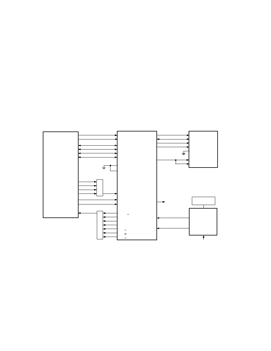
ADV611/ADV612
30
REV. 0
APPLYING THE ADV611/ADV612
This section includes the following topics:
· Using the ADV611/ADV612 in computer applications
· Using the ADV611/ADV612 in stand-alone applications
· Configuring the host interface for 16- or 32-bit data paths
· Connecting the video interface to popular video encoders and
decoders
· Getting the most out of the ADV611/ADV612
The following Analog Devices products should be considered in
ADV611/ADV612 designs:
· ADV7175/ADV7176--Digital YUV to analog composite
video encoder
· AD722--Analog RGB to analog composite video encoder
· AD1843--Audio codec with embedded video synchronization
· ADSP-21xx--Family of fixed-point digital signal processors
· AD8xxx--Family of video operational amplifiers
Using the ADV611/ADV612 in Computer Applications
Many key features of the ADV611/ADV612 were driven by the
demanding cost and performance requirements of computer
applications. The following ADV611/ADV612 features provide
key advantages in computer applications, such as the one in
Figure 15.
· Host Interface
The 512 double word FIFO provides necessary buffering of
compressed digital video to deal with PCI bus latency.
· Low Cost External DRAM
Unlike many other real-time compression solutions, the
ADV611/ADV612 does not require expensive external
SRAM transform buffers or VRAM frame stores.
A2
A3
D0D7
D8D15
D16D23
D24D31
A28
A29
A30
A31
HOST BUS
RD
WR
DECODE
1
DECODE
2
VCLK
VDATA [07]
LLC
XTAL
SAA7111
27MHz PAL OR NTSC
ADR0
ADR1
DQ0DQ7
DQ8DQ15
DQ16DQ23
DQ24DQ31
CS
STATS R
LCODE
24.576MHz
XTAL
A0A8
D0D15
A0A8
DQ1DQ16
NOTE:
DECODE
1
ASSERTS CS
~
ON THE
ADV611/ADV612 FOR HOST ADDRESSES
0X4000,0000 THROUGH 0X4000,0013
DECODE
2
IS HOST-SPECIFIC
ADV611/ADV612
DRAM
(256K 16-BIT)
COMPOSITE VIDEO INPUT
VCLKO
TOSHIBA TC514265DJ/DZ/DFT-60
NEC
PD424210ALE-60
NEC
PD42S4210ALE-60
HITACHI
HM514265CJ-60
ANY DRAM USED WITH THE ADV611/ADV612
MUST MEET THE MINIMUM SPECIFICATIONS
OUTLINED FOR THE HYPER MODE DRAMS
LISTED
FIFO SRQ
FIFO STP
FIFO ERR
Y[07]
BE0BE1
BE2BE3
RD
WR
HIRQ
RAS
CAS
WE
RAS
CAS
OE
WEL
WEH
ACK
Figure 15. A Suggested PC Application Design
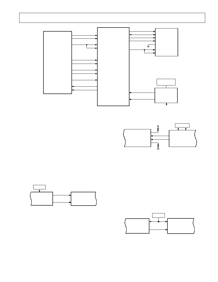
ADV611/ADV612
31
REV. 0
(MODE 0 & SLAVE MODE)
(CCIR-656 MODE)
XTAL
10k
150
VCLK
XTAL
ADV611/ADV612
VCLKO
CLOCK
P7P0
ADV7175
BLANK
ALSB
VDATA (7:0)
Figure 18. ADV611/ADV612 and ADV7175 Example
Interfacing Block Diagram
Using the Raytheon TMC22153 Video Decoder
Raytheon has a whole family of video parts. Any member of the
family can be used. The user must select the part needed based
on the requirements of the application. Because the Raytheon
part does not include the A/Ds, an external A/D is necessary in
this design (or a pair of A/Ds for S video).
The part can be used in CCIR-656 (D1) mode for a zero con-
trol signal interface. Special attention must be paid to the video
output modes in order to get the right data to the right pins (see
the following diagram).
Note that the circuit in Figure 19 has not been built or tested.
MODE SET TO:
CDEC = 1
YUVT
= 1
F422
= X
TMC22153
Y(2:9)
CLOCK
XTAL
VCLK
VCLK
VDATA (0:7)
ADV611/ADV612
(CCIR-656 & SLAVE MODE)
Figure 19. ADV611/ADV612 and TMC22153 Example
CCIR-656 Mode Interface
FL0
FL1
ADR0
ADR1
D8D23
D0D15
D16D31
PF4
FL2
CS
RD
RD
LCODE
IRQ2
IRQL1
HIRQ
A0A8
D0D15
A0A8
DQ1DQ16
THE ADSP-2185 INTERNAL CLOCK RATE
DOUBLE THE INPUT CLOCK
*THE INPUT CLOCK RATE = 1/2 OF THE INTERNAL
CLOCK RATE, RANGING FROM 12 TO 21MHz
ADV611/ADV612
ADSP-2185
DRAM
(256K 16-BIT)
TOSHIBA TC514265DJ/DZ/DFT-60
NEC
PD424210ALE-60
NEC
PD42S4210ALE-60
HITACHI
HM514265CJ-60
ANY DRAM USED WITH THE ADV611/ADV612
MUST MEET THE MINIMUM SPECIFICATIONS
OUTLINED FOR THE HYPER MODE DRAMS
LISTED
WR
WR
PF5
BE2
BE3
RAS
CAS
WE
RAS
CAS
OE
WEL
WEH
VCLK
VDATA [07]
LLC
XTAL
SAA7111
COMPOSITE VIDEO INPUT
Y[07]
BE0
BE1
27MHz PAL OR NTSC
24.576MHz
XTAL
Figure 16. Alternate Stand-Alone Application Design
Using the ADV611/ADV612 In Stand-Alone Applications
Figure 16 shows the ADV611/ADV612 in a noncomputer
based applications. Here, an ADSP-2185 digital signal proces-
sor provides Host control and BW calculation services. Note
that all control and BW operations occur over the host interface
in this design.
Connecting the ADV611/ADV612 to Popular Video Decoders
and Encoders
The following circuits are recommendations only. Analog
Devices has not actually built or tested these circuits.
Using the Philips SAA7111 Video Decoder
The SAA7111 example circuit, which appears in Figure 17, is
used in this configuration on the ADV611 CCTVPIPE demon-
stration board.
XTAL
(CCIR-656 MODE)
SAA7111
Y(0:7)
LLC
XTAL
VCLK
VDATA (0:7)
ADV611/ADV612
Figure 17. ADV611/ADV612 and SAA7111 Example
Interfacing Block Diagram
Using the Analog Devices ADV7175 Video Encoder
Because the ADV7175 has a CCIR-656 interface, it connects
directly with the ADV611/ADV612 without "glue" logic. Note
that the ADV7175 can only be used at CCIR-601 sampling
rates.
The ADV7175 example circuit, which appears in Figure 18, is
used in this configuration on the ADV611 CCTVPIPE demon-
stration board.
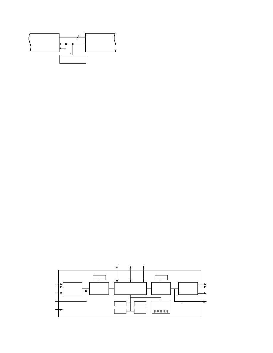
ADV611/ADV612
32
REV. 0
HARRIS
8115
CLK2
27MHz
PIXEL CLOCK GSC
VCLK
VDATA (07)
ADV611/ADV612
CLK2
P8P15
8
Figure 20. Using the Harris 8115 Decoder
GETTING THE MOST OUT OF ADV611/ADV612
How Much Compression Can Be Expected
The ADV611/ADV612 can be used in applications where up
to 7500:1 compression is required. To express this in more
meaningful terms, a digitized NTSC video signal at 167 MBit/s
per second can be reduced to less than 25 kbits per second. To
achieve this performance, the following approach could be used:
1. Image Compressed to 250:1
2. Frame Rate Reduced to 1 frame per second (not uncommon
in CCTV applications)
3. Quality box size less than 1% of the total image size
4. Background contrast attenuated by 18 dB
The scenario described above used by Analog Devices on the
CCTVPIPE evaluation board as the splash-screen after power-
up. Video quality is subjective, and therefore, it is highly recom-
mended to perform a direct evaluation of the CCTVPIPE or the
ADV601 software codec to confirm that the compression per-
formance is appropriate for a given application.
While the ADV611/ADV612 can be used in very high compres-
sion applications as outlined above, it is equally suitable for full
resolution, 60 field per second visually loss-less applications.
Evaluation Board
There is a low cost stand-alone evaluation board for the ADV611
called the CCTVPIPE (see block diagram). The CCTVPIPE
provides a fast, simple, and low cost means of evaluating the
performance of the ADV611/ADV612 and it is very similar to
the evaluation board for the ADV601LC, the VideoPipe. The
CCTVPIPE is shipped with a small mouse to allow real-time
quality box control. The board is also shipped with a small
speaker to provide an audio alert signal when motion is detected
in the video image. All of the source code and schematics for the
CCTVPIPE are available from the Analog Devices Web site free
of charge (www.analog.com/wavelet).
The exact part number is ADV611-CCTVPIPE and it can be
purchased through any Analog Devices authorized sales channel.
A PCI card is available for the ADV601 called the "VideoLab,"
which is bitstream compatible with the ADV611/ADV612. See
the Analog Devices Web site for further details.
Software Codec
Analog Devices has created two types of software products for
cases where encoding or decoding in software are desirable.
· Bit Exact Codec Nonreal-time bit exact encoder for
Windows
®
'95 or '98.
· MMX/DirectShow Player Real-time playback for
Windows '98 (PC monitor can be used to view the video
directlyno need for a dedicated TV monitor).
Field Rate Reduction
As demonstrated by the CCTVPIPE evaluation board, field
rates can be reduced to increase compression. The ADV611/
ADV612 allow this to be done in hardware (see register
descriptions).
Edge Enhancement and Detection
Since the ADV611/ADV612 filters the image into wavelet
subbands, edge information is isolated in the high pass blocks of
image data (see the Mallat diagram of the Analog Devices build-
ing in the ADV601LC data sheet for an illustration). By zeroing
the low pass blocks, the ADV611/ADV612 will preserve only
the high pass content of the image and thus enhance the edges
in the image. The CCTVPIPE has a mode that demonstrates
this feature. Furthermore, these blocks can be Huffman de-
coded and analyzed for edge detection purposes.
Motion Detection
There are two known means of implementing motion detection
with the ADV611/ADV612.
1. Compare the image statistics between fields of video. This is
the technique used on the CCTVPIPE for the motion detec-
tion demo.
2. Decode the smallest Mallat block (Block 39) and compare
one field to the next. Since these block are small (approximately
2400 pixels) the computational burden is much less than it
would be for the entire image. For comparative purposes, the
data samples in Block 39 contain only 1/1024th of the total
samples, or 1/512th the luminance samples. Please Contact
Analog Device, Inc. for information on how to implement
this technique with quality box placement.
SERIAL PORT
(SPORT)
JP17
DRAM
ADSP-2185
H/W RESET
EZ-ICE
JP16
RS-232
P1
ADV611
H/W RESET
ADV7175
DRAM
ADV611
H/W RESET
SAA7111
Y/C
J2
CVBS
J11
SRAM
ROM
SRAM
PALS
RESET
FREEZE
UP
DOWN
SELECT
PUSH
BUTTONS
CCIR-656
J12
+5VDC
J10
ADV611
CCTVPIPE
Y/C
J8
CVBS
J7
CCIR-656
J13
Figure 21. ADV611 CCTVPIPE Block Diagram
Windows is a registered trademark of Microsoft Corporation.
33
REV. 0
ADV611/ADV612
The ADV611/ADV612 Video Codec uses a Bi-Orthogonal (7, 9) Wavelet Transform.
RECOMMENDED OPERATING CONDITIONS
Parameter
Description
Min
Max
Unit
V
DD
Supply Voltage
4.50
5.50
V
T
AMB
Ambient Operating Temperature
0
+70
°
C
ELECTRICAL CHARACTERISTICS
Parameter
Description
Test Conditions
Min
Max
Unit
V
IH
Hi-Level Input Voltage
@ V
DD
= max
2.0
N/A
V
V
IL
Lo-Level Input Voltage
@ V
DD
= min
N/A
0.8
V
V
OH
Hi-Level Output Voltage
@ V
DD
= min, I
OH
= 0.5 mA
2.4
N/A
V
V
OL
Lo-Level Output Voltage
@ V
DD
= min, I
OL
= 2 mA
N/A
0.4
V
I
IH
Hi-Level Input Current
@ V
DD
= max, V
IN
= V
DD
max
N/A
10
µ
A
I
IL
Lo-Level Input Current
@ V
DD
= max, V
IN
= 0 V
N/A
10
µ
A
I
OZH
Three-State Leakage Current
@ V
DD
= max, V
IN
= V
DD
max
N/A
10
µ
A
I
OZL
Three-State Leakage Current
@ V
DD
= max, V
IN
= 0 V
N/A
10
µ
A
C
I
Input Pin Capacitance
@ V
IN
= 2.5 V, f
IN
= 1.0 MHz, T
AMB
= +25
°
C
N/A
8*
pF
C
O
Output Pin Capacitance
@ V
IN
= 2.5 V, f
IN
= 1.0 MHz, T
AMB
= +25
°
C
N/A
8*
pF
*Guaranteed but not tested.
ABSOLUTE MAXIMUM RATINGS*
Parameter
Description
Min
Max
Unit
V
DD
Supply Voltage
0.3
+7
V
V
IN
Input Voltage
N/A
V
DD
±
0.3
V
V
OUT
Output Voltage
N/A
V
DD
±
0.3
V
T
AMB
(ADV611)
Ambient Operating Temperature
0
+70
°
C
T
AMB
(ADV612)
Ambient Operating Temperature
25
+85
°
C
T
S
Storage Temperature
65
+150
°
C
T
L
Lead Temperature (5 sec) PQFP
N/A
+280
°
C
*Stresses greater than those listed above under Absolute Maximum Ratings may cause permanent damage to the device. This is a stress rating only; functional opera-
tion of the device at these or any other conditions above those indicated in the Pin Definitions section of this specification is not implied. Exposure to maximum
rating conditions for extended periods may affect device reliability.
SUPPLY CURRENT AND POWER
Parameter
Description
Test Conditions
Min
Max
Unit
I
DD
Supply Current (Dynamic)
@ V
DD
= max, t
VCLK
_
CYC
= 37 ns (at 27 MHz VCLK)
0.11
0.27
A
I
DD
Supply Current (Soft Reset)
@ V
DD
= max, t
VCLK
_
CYC
= 37 ns (at 27 MHz VCLK)
0.08
0.17
A
I
DD
Supply Current (Idle)
@ V
DD
= max, t
VCLK
_
CYC
= None
0.01
0.02
A
ENVIRONMENTAL CONDITIONS
Parameter
Description
ADV611/ADV612 Max
Unit
CA
Case-to-Ambient Thermal Resistance
30
°
C/W
JA
Junction-to-Ambient Thermal Resistance
35
°
C/W
JC
Junction-to-Case Thermal Resistance
5
°
C/W
SPECIFICATIONS
CAUTION
The ADV611/ADV612 is an ESD (electrostatic discharge) sensitive device. Electrostatic charges readily
accumulate on the human body and equipment and can discharge without detection. Permanent
damage may occur to devices subjected to high energy electrostatic discharges. Proper ESD
precautions are strongly recommended to avoid functional damage or performance degradation.
The ADV611/ADV612 latchup immunity has been demonstrated at
200 mA/200 mA on all pins
when tested to industry standard/JEDEC methods.
WARNING!
ESD SENSITIVE DEVICE
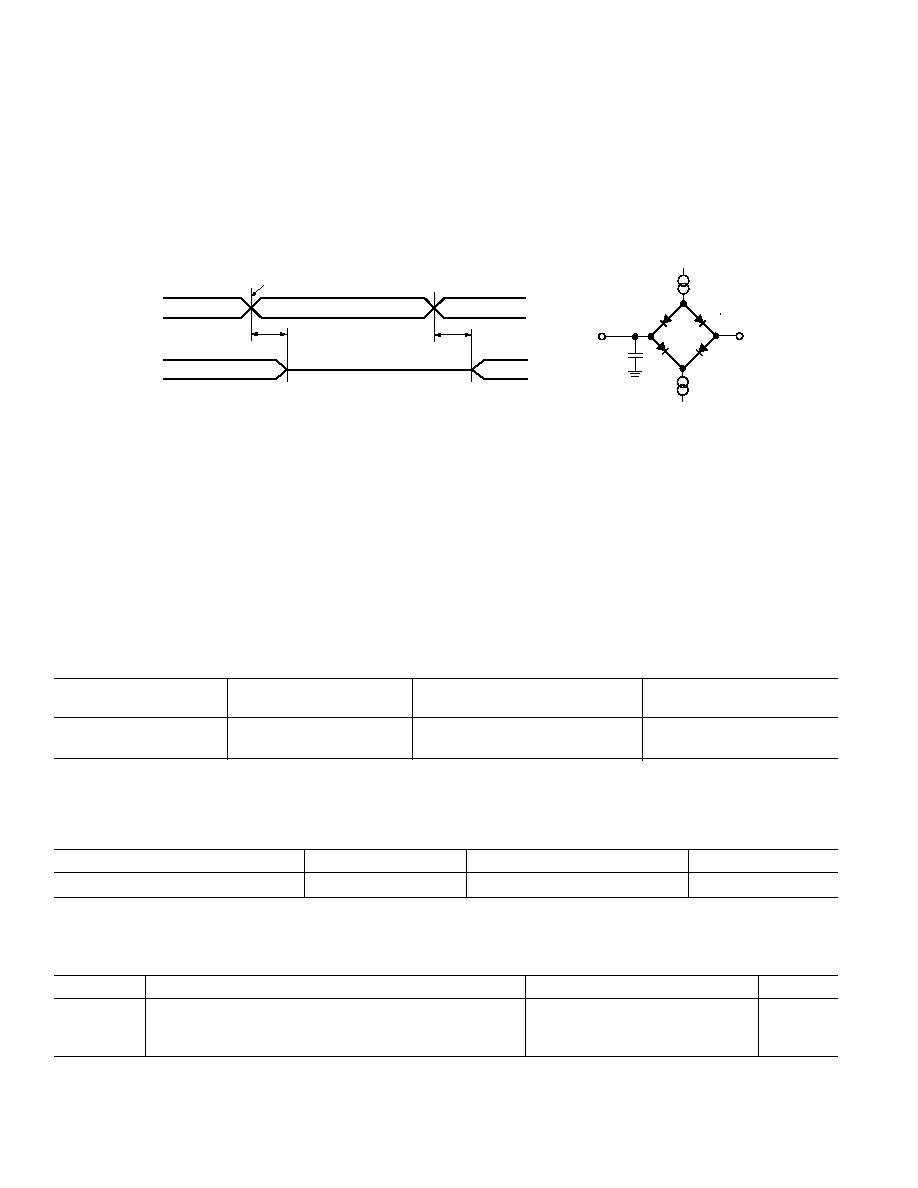
ADV611/ADV612
34
REV. 0
TIMING PARAMETERS
This section contains signal timing information for the ADV611/ADV612. Timing descriptions for the following items appear in this
section:
· Clock signal timing
· Video data transfer timing (CCIR-656, and Multiplexed Philips formats)
· Host data transfer timing (direct register read/write access)
Clock Signal Timing
The diagram in this section shows timing for VCLK input and VCLKO output. All output values assume a maximum pin
loading of 50 pF.
Table XVII. Video Clock Period, Frequency, Drift and Jitter
Min VCLK_CYC
Nominal VCLK_CYC
Max VCLK_CYC
Video Format
Period
Period (Frequency)
Period
1, 2
CCIR-601 PAL
35.2 ns
37 ns (27 MHz)
38.9 ns
CCIR-601 NTSC
35.2 ns
37 ns (27 MHz)
38.9 ns
NOTES
1
VCLK Period Drift =
±
0.1 (VCLK_CYC/field.
2
VCLK edge-to-edge jitter = 1 ns.
Table XVIII. Video Clock Duty Cycle
Min
Nominal
Max
VCLK Duty Cycle
1
(40%)
(50%)
(60%)
NOTE
1
VCLK Duty Cycle = t
VCLK_HI
/(t
VCLK_LO
)
×
100.
Table XIX. Video Clock Timing Parameters
Parameter
Description
Min
Max
Unit
t
VCLK_CYC
VCLK Signal, Cycle Time (1/Frequency) at 27 MHz
(See Video Clock Period Table)
t
VCLKO_D0
VCLKO Signal, Delay (when VCLK2 = 0) at 27 MHz
10
29
ns
t
VCLKO_D1
VCLKO Signal, Delay (when VCLK2 = 1) at 27 MHz
10
29
ns
TEST CONDITIONS
Figure 22 shows test condition voltage reference and device
loading information. These test conditions consider an output
as disabled when the output stops driving and goes from the
measured high or low voltage to a high impedance state. Tests
measure output disable time (t
DISABLE
) as the time between the
reference input signal crossing +1.5 V and the time that the
output reaches the high impedance state (also +1.5 V). Simi-
larly, these tests conditions consider an output as enabled when
the output leaves the high impedance state and begins driving a
measured high or low voltage. Tests measure output enable time
(t
ENABLE
) as the time between the reference input signal crossing
+1.5 V and the time that the output reaches the measured high
or low voltage.
INPUT
REFERENCE
SIGNAL
OUTPUT
SIGNAL
t
DISABLED
t
ENABLED
1.5V
V
OH
V
OL
V
IH
V
IL
1.5V
INPUT & OUTPUT VOLTAGE/TIMING REFERENCES
DEVICE LOADING FOR AC MEASUREMENTS
TO
OUTPUT
PIN
2pF
+1.5V
I
OL
I
OH
Figure 22. Test Condition Voltage Reference and Device Loading
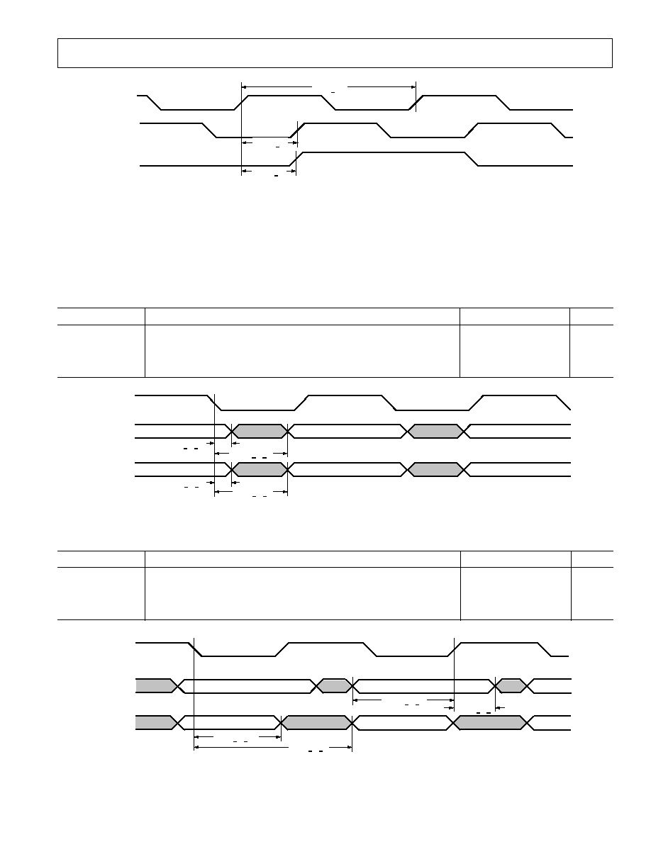
ADV611/ADV612
35
REV. 0
CCIR-656 Video Format Timing
The diagrams in this section show transfer timing for pixel (YCrCb), line (horizontal), and frame (vertical) data in CCIR-656 video
mode. All output values assume a maximum pin loading of 50 pF. Note that in timing diagrams for CCIR-656 video, the label CTRL
indicates the VSYNC, HSYNC, and FIELD pins.
Table XX. CCIR-656 Video--Decode Pixel (YCrCb) Timing Parameters
Parameter
Description
Min
Max
Units
t
VDATA_DC_D
VDATA Signals, Decode CCIR-656 Mode, Delay
N/A
14
ns
t
VDATA_DC_OH
VDATA Signals, Decode CCIR-656 Mode, Output Hold
4
N/A
ns
t
CTRL_DC_D
CTRL Signals, Decode CCIR-656 Mode, Delay
N/A
11
ns
t
CTRL_DC_OH
CTRL Signals, Decode CCIR-656 Mode, Output Hold
5
N/A
ns
(O) CTRL
(O) VCLKO
t
CTRL DC OH
(O) VDATA
t
VDATA DC OH
VALID
VALID
VALID
VALID
VALID
VALID
t
CTRL DC D
t
VDATA DC D
Figure 24. CCIR-656 Video--Decode Pixel (YCrCb) Transfer Timing
Table XXI. CCIR-656 Video--Encode Pixel (YCrCb) Timing Parameters
Parameter
Description
Min
Max
Units
t
VDATA_EC_S
VDATA Bus, Encode CCIR-656 Mode, Setup
2
N/A
ns
t
VDATA_EC_H
VDATA Bus, Encode CCIR-656 Mode, Hold
5
N/A
ns
t
CTRL_EC_D
CTRL Signals, Encode CCIR-656 Mode, Delay
N/A
33
ns
t
CTRL_EC_OH
CTRL Signals, Encode CCIR-656 Mode, Output Hold
20
N/A
ns
t
VDATA EC H
(O) CTRL
(I) VCLK
(I) VDATA
ASSERTED
VALID
ASSERTED
VALID
t
CTRL EC OH
t
CTRL EC D
t
VDATA EC S
Figure 25. CCIR-656 Video--Encode Pixel (YCrCb) Transfer Timing
(I) VCLK
(O) VCLKO
(VCLK2 = 0)
(I) VCLKO
(VCLK2 = 1)
t
VCLK CYC
t
VCLKO D0
t
VCLKO D1
NOTE:
USE VCLK FOR CLOCKING VIDEO-ENCODE OPERATIONS AND USE VCLKO FOR CLOCKING VIDEO-DECODE OPERATIONS.
DO NOT TRY TO USE EITHER CLOCK FOR BOTH ENCODE AND DECODE.
Figure 23. Video Clock Timing
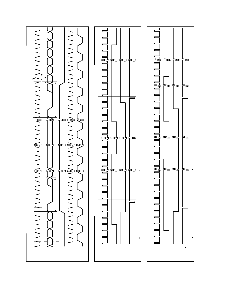
ADV611/ADV612
36
REV. 0
Figure 26. CCIR-656 Video--Line (Horizontal) and Frame (Vertical) Transfer Timing
Note that for CCIR-656 Video--Decode and Master Line (Horizontal) timing, VDATA is synchronous with VCLKO.
(O) STATS_R
(ENCODE)
(O) HSYNC
(O) VSYNC
(O) FIELD
625 (PAL)
LINE #
621
622
623
624
625
1
2
3
4
5
6
310
311
312
313
314
315
316
317
318
319
21
22
23
24
309
ENCODE / DECODE & MASTER CCIR-656 -- 625 (PAL) F
RAME (VERTICAL) TRANSFER TIMING
334
335
336
337
(NOTE: STATS
R IS ALWAYS LO FOR 45 CYCLES BEFORE GOING HI AGAIN. STATS
R IS LO COMING OUT OF SOFT RESET AND GOES HIGH RIGHT AFTER THE ADV611/ADV612 FINISHES TAKING IN THE VERY FIRST FIELD.)
(O) HSYNC
(I) VCLK
(I) VDATA
FF
XX
FF
XX
SAMPLE 0
NTSC CCIR-601 PIXEL, N = 720
(O) VCLKO
(VCLK2 = 0)
(O) VCLKO
(VCLK2 = 1)
ENCODE CCIR-656 -- LINE (HORIZONTAL) TRANSFER TIMING (FOR DECODE VDATA IS SYNCHRONOUS TO VCLKO)
t
VDATA
EC
H
t
VDATA
EC
S
Y
2
PAL CCIR-601 PIXEL, N = 720
Cr
0
Y
1
Y
0
Cb
2
Cb
0
Y
N-2
Cb
N-2
Cr
N-2
Y
N-1
EAV
SAV
(O) STATS
R
(ENCODE)
(O) HSYNC
(O) VSYNC
(O) FIELD
525 (NTSC)
LINE #
524
525
123456789
2
6
3
2
6
4
2
6
5
2
6
6
2
6
7
2
6
8
282
283
284
262
335
336
337
338
ENCODE / DECODE CCIR-656 -- 525 (NTSC) F
RAME (VERTICAL) TRANSFER TIMING
(NOTE: STATS
R IS ALWAYS LO FOR 45 CYCLES BEFORE GOING HI AGAIN. STATS
R IS LO COMING OUT OF SOFT RESET AND GOES HIGH RIGHT AFTER THE ADV611/ADV612 FINISHES TAKING IN THE VERY FIRST FIELD.)
20
21
22
23
ADV611/ADV612
37
REV. 0
Multiplexed Philips Video Timing
The diagrams in this section show transfer timing for pixel (YCrCb) data in Multiplexed Philips video mode. For line (horizontal)
and frame (vertical) data transfer timing, see Figure 29. All output values assume a maximum pin loading of 50 pF. Note that in
timing diagrams for Multiplexed Philips video, the label CTRL indicates the VSYNC, HSYNC and FIELD pins.
Table XXII. Multiplexed Philips Video--Decode and Master Pixel (YCrCb) Timing Parameters
Parameter
Description
Min
Max
Unit
t
VDATA_DMM_D
VDATA Bus, Decode Master Multiplexed Philips, Delay
N/A
14
ns
t
VDATA_DMM_OH
VDATA Bus, Decode Master Multiplexed Philips, Output Hold
4
N/A
ns
t
CTRL_DMM_D
CTRL Signals, Decode Master Multiplexed Philips, Delay
N/A
11
ns
t
CTRL_DMM_OH
CTRL Signals, Decode Master Multiplexed Philips, Output Hold
5
N/A
ns
(O) CTRL
(O) VCLKO
t
CTRL DMM OH
(O) VDATA
t
VDATA DMM OH
VALID
VALID
VALID
VALID
VALID
VALID
t
VDATA DMM D
t
CTRL DMM D
Figure 27. Multiplexed Philips Video--Decode and Master Pixel (YCrCb) Transfer Timing
Table XXIII. Multiplexed Philips Video--Decode and Slave Pixel (YCrCb) Timing Parameters
Parameter
Description
Min
Max
Unit
t
VDATA_DSM_D
VDATA Bus, Decode Slave Multiplexed Philips, Delay
N/A
14
ns
t
VDATA_DSM_OH
VDATA Bus, Decode Slave Multiplexed Philips, Output Hold
4
N/A
ns
t
CTRL_DSM_S
CTRL Signals, Decode Slave Multiplexed Philips, Setup
16
N/A
ns
t
CTRL_DSM_H
CTRL Signals, Decode Slave Multiplexed Philips, Hold
42
N/A
ns
(I) CTRL
(O) VCLKO
(O) VDATA
t
CTRL DSM H
VALID
VALID
VALID
VALID
t
CTRL DSM S
t
VDATA DSM OH
t
VDATA DSM D
Figure 28. Multiplexed Philips Video--Decode and Slave Pixel (YCrCb) Transfer Timing
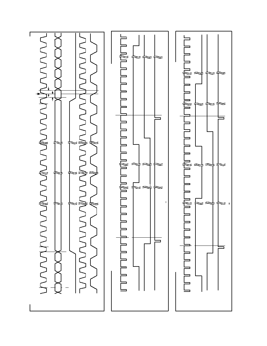
ADV611/ADV612
38
REV. 0
Figure 29. Multiplexed Philips VideoLine (Horizontal) and Frame (Vertical) Transfer Timing
STATS
_
R
(ENCODE)
HSYNC
VSYNC
625 (PAL)
LINE #
621
622
623
624
625
1
2
3
4
5
6
310
311
312
313
314
315
316
317
318
319
8
23
24
309
7
320
321
(NOTE: STATS_R IS ALWAYS LO FOR 45 CYCLES BEFORE GOING HI AGAIN. STATS
R IS LO COMING OUT OF SOFT RESET AND GOES HIGH RIGHT AFTER THE ADV611/ADV612 FINISHES TAKING IN THE VERY FIRST FIELD.)
ENCODE / DECODE & MASTER MULTIPLEXED P
HILIPS -- 625 (PAL) FRAME (VERTICAL) TRANSFER TIMING
335
336
(NOTE: ADV611/ADV612
GETS HSYNCH FROM PHILIPS HREF)
(O) FIELD
STATS_R
(ENCODE)
HSYNC
VSYNC
525 (NTSC)
LINE #
524
525
1
2
3
4
5
6
7
8
9
263
264
265
266
267
268
262
335
336
337
338
ENCODE / DECODE & MASTER MULTIPLEXED P
HILIPS -- 525 (NTSC) F
RAME (VERTICAL) TRANSFER TIMING
282
283
284
22
23
24
21
(NOTE: STATS_R IS ALWAYS LO FOR 45 CYCLES BEFORE GOING HI AGAIN. STATS
R IS LO COMING OUT OF SOFT RESET AND GOES HIGH RIGHT AFTER THE ADV611/ADV612 FINISHES TAKING IN THE VERY FIRST FIELD.)
(O) FIELD
(NOTE: ADV611/ADV612
IN SLAVE MODE GETS HSYNCH FROM PHILIPS HREF)
(O) HSYNC
(I) VCLK
(I) VDATA
SAMPLE 0
NTSC CCIR-601 PIXEL, N = 720
(O) VCLKO
(VCLK2 = 0)
(O) VCLKO
(VCLK2 = 1)
t
VDATA_EC_H
t
VDATA_EC_S
Y
2
PAL CCIR-601 PIXEL, N = 720
Cr
0
Y
1
Y
0
Cb
2
Cb
0
Y
N-2
Cb
N-2
Cr
N-2
Y
N-1
ENCODE MASTER MULTIPLEXED PHILIPS -- LINE (HORIZONTAL) TRANSFER TIMING (FOR DECODE VDATA IS SYNCHRONOUS TO VCLKO)
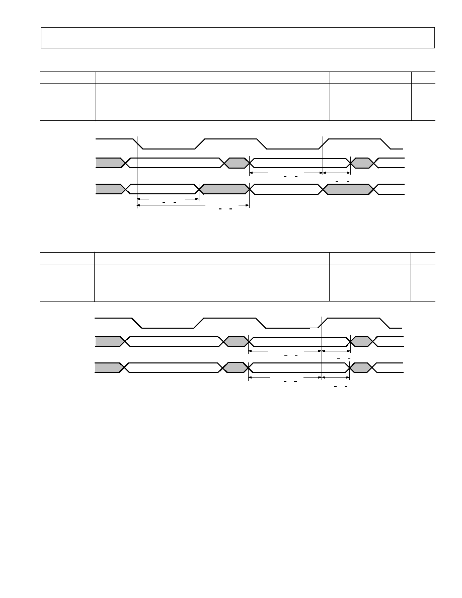
ADV611/ADV612
39
REV. 0
Table XXIV. Multiplexed Philips Video--Encode and Master Pixel (YCrCb) Timing Parameters
Parameter
Description
Min
Max
Unit
t
VDATA_EMM_S
VDATA Bus, Encode Master Multiplexed Philips, Setup
2
N/A
ns
t
VDATA_EMM_H
VDATA Bus, Encode Master Multiplexed Philips, Hold
5
N/A
ns
t
CTRL_EMM_D
CTRL Signals, Encode Master Multiplexed Philips, Delay
N/A
33
ns
t
CTRL_EMM_OH
CTRL Signals, Encode Master Multiplexed Philips, Output Hold
20
N/A
ns
(O) CTRL
(I) VCLK
(I) VDATA
ASSERTED
VALID
ASSERTED
VALID
t
VDATA EMM H
t
CTRL EMM OH
t
CTRL EMM D
t
VDATA EMM S
Figure 30. Multiplexed Philips Video--Encode and Master Pixel (YCrCb) Transfer Timing
Table XXV. Multiplexed Philips Video--Encode and Slave Pixel (YCrCb) Timing Parameters
Parameter
Description
Min
Max
Unit
t
VDATA_ESM_S
VDATA Bus, Encode Slave Multiplexed Philips Mode, Setup
2
N/A
ns
t
VDATA_ESM_H
VDATA Bus, Encode Slave Multiplexed Philips Mode, Hold
5
N/A
ns
t
CTRL_ESM_S
CTRL Signals, Encode Slave Multiplexed Philips Mode, Setup
5
N/A
ns
t
CTRL_ESM_H
CTRL Signals, Encode Slave Multiplexed Philips Mode, Hold
5
N/A
ns
(I) CTRL
(I) VCLK
(I) VDATA
t
CTRL ESM H
ASSERTED
t
VDATA ESM H
VALID
ASSERTED
VALID
t
VDATA ESM S
t
CTRL ESM S
Figure 31. Multiplexed Philips Video--Encode and Slave Pixel (YCrCb) Transfer Timing
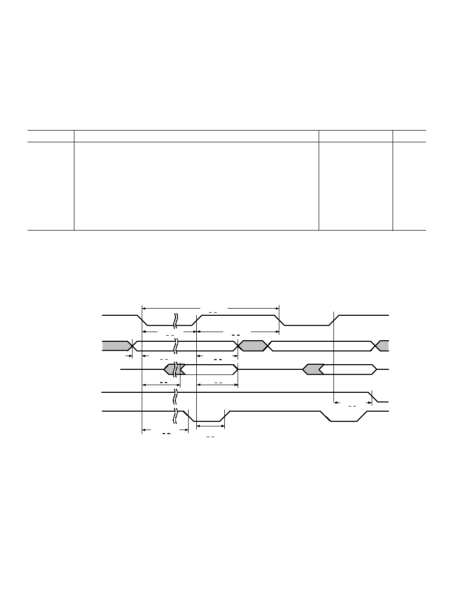
ADV611/ADV612
40
REV. 0
Host Interface (Indirect Address, Indirect Register Data and Interrupt Mask/Status) Register Timing
The diagrams in this section show transfer timing for host read and write accesses to all of the ADV611/ADV612's direct registers,
except the Compressed Data register. Accesses to the Indirect Address, Indirect Register Data, and Interrupt Mask/Status registers
are slower than access timing for the Compressed Data register. For information on access timing for the Compressed Data direct
register, see the Host Interface (Compressed Data) Register Timing section. Note that for accesses to the Indirect Address, Indirect
Register Data and Interrupt Mask/Status registers, your system MUST observe ACK and RD or WR assertion timing.
Table XXVI. Host (Indirect Address, Indirect Data, and Interrupt Mask/Status) Read Timing Parameters
Parameter
Description
Min
Max
Unit
t
RD_D_RDC
RD Signal, Direct Register, Read Cycle Time (at 27 MHz VCLK)
N/A
1
N/A
ns
t
RD_D_PWA
RD Signal, Direct Register, Pulsewidth Asserted (at 27 MHz VCLK)
N/A
1
N/A
ns
t
RD_D_PWD
RD Signal, Direct Register, Pulsewidth Deasserted (at 27 MHz VCLK)
5
N/A
ns
t
ADR_D_RDS
ADR Bus, Direct Register, Read Setup
2
N/A
ns
t
ADR_D_RDH
ADR Bus, Direct Register, Read Hold
2
N/A
ns
t
DATA_D_RDD
DATA Bus, Direct Register, Read Delay
N/A
171.6
2, 3
ns
t
DATA_D_RDOH
DATA Bus, Direct Register, Read Output Hold (at 27 MHz VCLK)
26
N/A
ns
t
RD_D_WRT
WR Signal, Direct Register, Read-to-Write Turnaround (at 27 MHz VCLK)
48.7
4
N/A
ns
t
ACK_D_RDD
ACK Signal, Direct Register, Read Delayed (at 27 MHz VCLK)
8.6
287.1
5, 6
ns
t
ACK_D_RDOH
ACK Signal, Direct Register, Read Output Hold (at 27 MHz VCLK)
11
N/A
ns
NOTES
1
RD input must be asserted (low) until ACK is asserted (low).
2
Maximum t
DATA_D_RDD
varies with VCLK according to the formula: t
DATA_D_RDD
(MAX)
= 4 (VCLK Period) +16.
3
During STATS_R deasserted (low) conditions, t
DATA_D_RDD
may be as long as 52 VCLK periods.
4
Minimum t
RD_D_WRT
varies with VCLK according to the formula: t
RD_D_WRT
(MIN)
= 1.5 (VCLK Period) 4.1.
5
Maximum t
ACK_D_RDD
varies with VCLK according to formula: t
ACK_D_RDD (MAX)
= 7 (VCLK Period) +14.8.
6
During STATS_R deasserted (low) conditions, t
ACK_D_RDD
may be as long as 52 VCLK periods.
VALID
VALID
VALID
VALID
(I) ADR,
BE
,
CS
(I)
RD
(O) DATA
(O)
ACK
(I)
WR
t
ADR D RDS
t
ACK D RDOH
t
RD D RDC
t
RD D PWA
t
RD D PWD
t
ADR D RDH
t
DATA D RDD
t
DATA D RDOH
t
RD D WRT
t
ACK D RDD
Figure 32. Host (Indirect Address, Indirect Register Data, and Interrupt Mask/Status) Read Transfer Timing
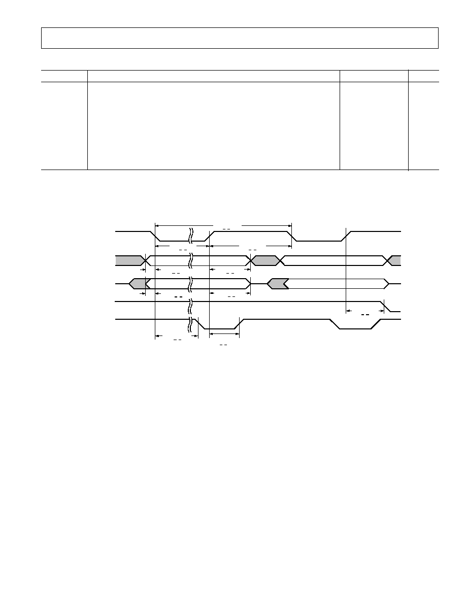
ADV611/ADV612
41
REV. 0
Table XXVII. Host (Indirect Address, Indirect Data and Interrupt Mask/Status) Write Timing Parameters
Parameter
Description
Min
Max
Unit
t
WR_D_WRC
WR Signal, Direct Register, Write Cycle Time (at 27 MHz VCLK)
N/A
1
N/A
ns
t
WR_D_PWA
WR Signal, Direct Register, Pulsewidth Asserted (at 27 MHz VCLK)
N/A
1
N/A
ns
t
WR_D_PWD
WR Signal, Direct Register, Pulsewidth Deasserted (at 27 MHz VCLK)
5
N/A
ns
t
ADR_D_WRS
ADR Bus, Direct Register, Write Setup
2
N/A
ns
t
ADR_D_WRH
ADR Bus, Direct Register, Write Hold
2
N/A
ns
t
DATA_D_WRS
DATA Bus, Direct Register, Write Setup
10
N/A
ns
t
DATA_D_WRH
DATA Bus, Direct Register, Write Hold
0
N/A
ns
t
WR_D_RDT
WR Signal, Direct Register, Read Turnaround (After a Write) (at 27 MHz VCLK)
35.6
2
N/A
ns
t
ACK_D_WRD
ACK Signal, Direct Register, Write Delay (at 27 MHz VCLK)
8.6
182.1
3, 4
ns
t
ACK_D_WROH
ACK Signal, Direct Register, Write Output Hold
11
N/A
ns
NOTES
1
WR input must be asserted (low) until ACK is asserted (low).
2
Minimum t
WR_D_RDT
varies with VCLK according to the formula: t
WR_D_RDT (MIN)
= 0.8 (VCLK Period) +7.4.
3
Maximum t
WR_D_WRD
varies with VCLK according to the formula: t
ACK_D_WRD (MAX)
= 4.3 (VCLK Period) +14.8.
4
During STATS_R deasserted (low) conditions, t
ACK_D_WRD
may be as long as 52 VCLK periods.
VALID
VALID
VALID
VALID
(I) ADR,
BE
,
CS
(I)
WR
(I) DATA
(O)
ACK
(I)
RD
t
ADR D WRS
t
DATA D WRS
t
WR D WRC
t
WR D PWA
t
WR D PWD
t
ADR D WRH
t
DATA D WRH
t
ACK D WRD
t
WR D RDT
t
ACK D WROH
Figure 33. Host (Indirect Address, Indirect Register Data, and Interrupt Mask/Status) Write Transfer Timing
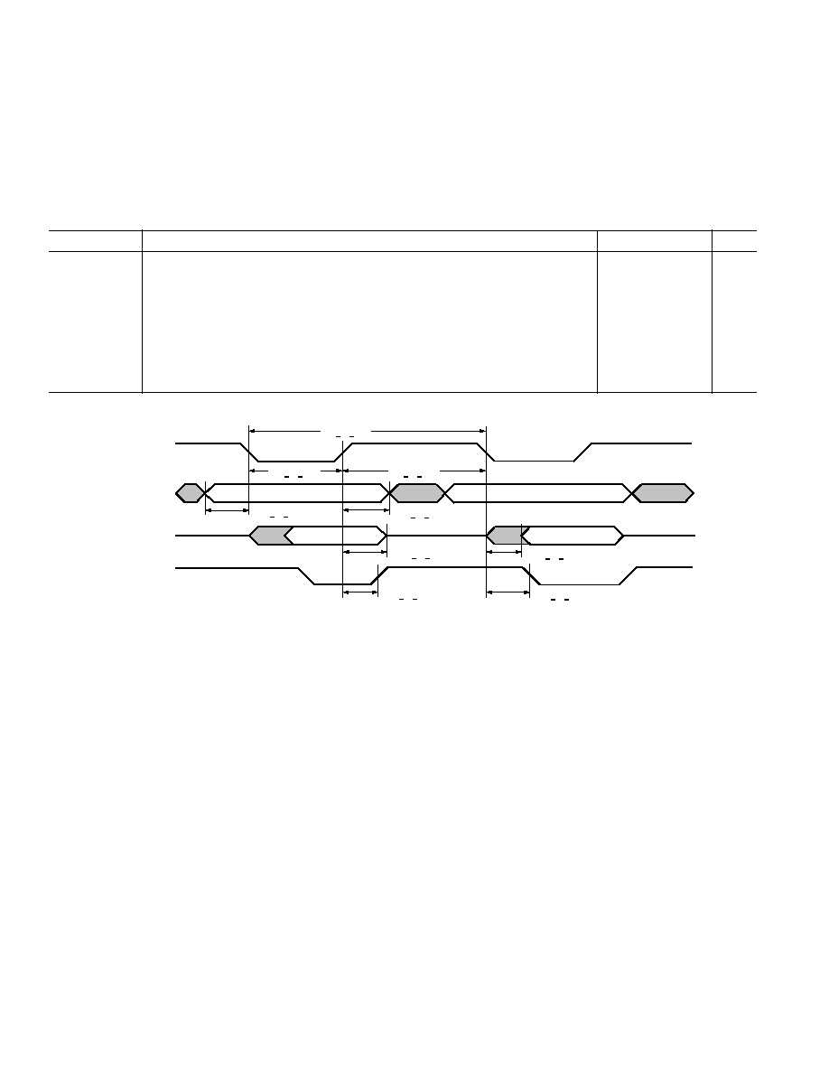
ADV611/ADV612
42
REV. 0
Host Interface (Compressed Data) Register Timing
The diagrams in this section show transfer timing for host read and write transfers to the ADV611/ADV612's Compressed Data
register. Accesses to the Compressed Data register are faster than access timing for the Indirect Address, Indirect Register Data, and
Interrupt Mask/Status registers. For information on access timing for the other registers, see the Host Interface (Indirect Address,
Indirect Register Data, and Interrupt Mask/Status) Register Timing section. Also note that as long as your system observes the RD
or WR signal assertion timing, your system does NOT have to wait for the ACK signal between new compressed data addresses.
Table XXVIII. Host (Compressed Data) Read Timing Parameters
Parameter
Description
Min
Max
Unit
t
RD_CD_RDC
RD Signal, Compressed Data Direct Register, Read Cycle Time
28
N/A
ns
t
RD_CD_PWA
RD Signal, Compressed Data Direct Register, Pulsewidth Asserted
10
N/A
ns
t
RD_CD_PWD
RD Signal, Compressed Data Direct Register, Pulsewidth Deasserted
10
N/A
ns
t
ADR_CD_RDS
ADR Bus, Compressed Data Direct Register, Read Setup
2
N/A
ns
t
ADR_CD_RDH
ADR Bus, Compressed Data Direct Register, Read Hold (at 27 MHz VCLK)
2
N/A
ns
t
DATA_CD_RDD
DATA Bus, Compressed Data Direct Register, Read Delay
N/A
10
ns
t
DATA_CD_RDOH
DATA Bus, Compressed Data Direct Register, Read Output Hold
18
N/A
ns
t
ACK_CD_RDD
ACK Signal, Compressed Data Direct Register, Read Delay
N/A
18
ns
t
ACK_CD_RDOH
ACK Signal, Compressed Data Direct Register, Read Output Hold
9
N/A
ns
(I) ADR,
BE
,
CS
(I)
RD
(O) DATA
(O)
ACK
VALID
VALID
VALID
VALID
t
ADR CD RDS
t
DATA CD RDD
t
ACK CD RDD
t
ACK CD RDOH
t
DATA CD RDOH
t
ADR CD RDH
t
RD CD RDC
t
RD CD PWA
t
RD CD PWD
Figure 34. Host (Compressed Data) Read Transfer Timing
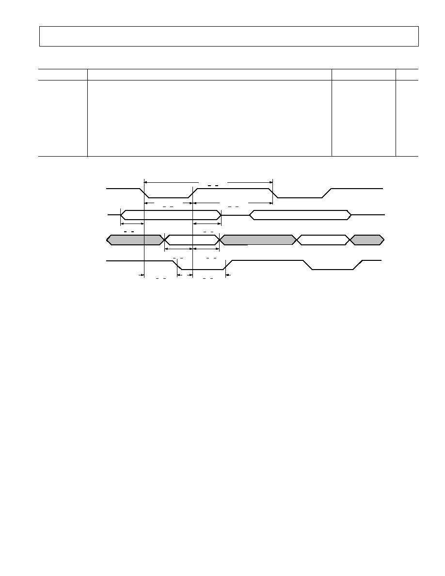
ADV611/ADV612
43
REV. 0
Table XXIX. Host (Compressed Data) Write Timing Parameters
Parameter
Description
Min
Max
Unit
t
WR_CD_WRC
WR Signal, Compressed Data Direct Register, Write Cycle Time
28
N/A
ns
t
WR_CD_PWA
WR Signal, Compressed Data Direct Register, Pulsewidth Asserted
10
N/A
ns
t
WR_CD_PWD
WR Signal, Compressed Data Direct Register, Pulsewidth Deasserted
10
N/A
ns
t
ADR_CD_WRS
ADR Bus, Compressed Data Direct Register, Write Setup
2
N/A
ns
t
ADR_CD_WRH
ADR Bus, Compressed Data Direct Register, Write Hold
2
N/A
ns
t
DATA_CD_WRS
DATA Bus, Compressed Data Direct Register, Write Setup
2
N/A
ns
t
DATA_CD_WRH
DATA Bus, Compressed Data Direct Register, Write Hold
2
N/A
ns
t
ACK_CD_WRD
ACK Signal, Compressed Data Direct Register, Write Delay
N/A
19
ns
t
ACK_CD_WROH
ACK Signal, Compressed Data Direct Register, Write Output Hold
9
N/A
ns
(I) ADR,
BE
,
CS
(I)
WR
(I) DATA
(O)
ACK
VALID
t
ADR CD WRH
t
ADR CD WRS
t
DATA CD WRS
t
DATA CD WRH
t
ACK CD WRD
t
WR CD WRC
t
ACK CD WROH
VALID
VALID
VALID
t
WR CD PWA
t
WR CD PWD
Figure 35. Host (Compressed Data) Write Transfer Timing

ADV611/ADV612
44
REV. 0
Pin
Pin
Pin
Name
Type
81
VDATA4
I/O
82
GND
GROUND
83
VDD
POWER
84
VDATA3
I/O
85
VDATA2
I/O
86
VDATA1
I/O
87
VDATA0
I/O
88
NC*
NC
89
NC*
NC
90
GND
GROUND
91
DATA31
I/O
92
DATA30
I/O
93
DATA29
I/O
94
DATA28
I/O
95
DATA27
I/O
96
DATA26
I/O
97
DATA25
I/O
98
DATA24
I/O
99
DATA23
I/O
100
DATA22
I/O
101
DATA21
I/O
102
DATA20
I/O
103
VDD
POWER
104
DATA19
I/O
105
DATA18
I/O
106
DATA17
I/O
107
DATA16
I/O
108
GND
GROUND
109
GND
GROUND
110
DATA15
I/O
111
DATA14
I/O
112
DATA13
I/O
113
DATA12
I/O
114
DATA11
I/O
115
DATA10
I/O
116
DATA9
I/O
117
DATA8
I/O
118
DATA7
I/O
119
DATA6
I/O
120
DATA5
I/O
Pin
Pin
Pin
Name
Type
41
CAS
O
42
WE
O
43
VDD
POWER
44
VDD
POWER
45
DDAT15
I/O
46
DDAT14
I/O
47
DDAT13
I/O
48
DDAT12
I/O
49
DDAT11
I/O
50
DDAT10
I/O
51
DDAT9
I/O
52
DDAT8
I/O
53
DDAT7
I/O
54
DDAT6
I/O
55
DDAT5
I/O
56
DDAT4
I/O
57
DDAT3
I/O
58
DDAT2
I/O
59
DDAT1
I/O
60
DDAT0
I/O
61
GND
GROUND
62
VDD
POWER
63
GND
GROUND
64
VDD
POWER
65
STALL
I
66
GND
GROUND
67
ENC
O
68
VCLKO
O
69
VDD
POWER
70
XTAL
I
71
VCLK
I
72
GND
GROUND
73
FIELD
I OR O
74
HSYNC
I OR O
75
VSYNC
I OR O
76
GND
GROUND
77
VDD
POWER
78
VDATA7
I/O
79
VDATA6
I/O
80
VDATA5
I/O
Pin
Pin
Pin
Name
Type
1
DATA4
I/O
2
DATA3
I/O
3
DATA2
I/O
4
DATA1
I/O
5
DATA0
I/O
6
VDD
POWER
7
GND
GROUND
8
RD
I
9
WR
I
10
CS
I
11
ADR1
I
12
ADR0
I
13
GND
GROUND
14
BE2BE3
I
15
BE0BE1
I
16
GND
GROUND
17
RESET
I
18
VDD
POWER
19
ACK
O
20
VDD
POWER
21
GND
GROUND
22
HIRQ
O
23
LCODE
O
24
FIFO_SRQ
O
25
STATS_R
O
26
VDD
POWER
27
GND
GROUND
28
GND
GROUND
29
VDD
POWER
30
DADR8
O
31
DADR7
O
32
DADR6
O
33
DADR5
O
34
DADR4
O
35
DADR3
O
36
DADR2
O
37
DADR1
O
38
DADR0
O
39
GND
GROUND
40
RAS
O
ADV611/ADV612 LQFP PINOUTS
*Apply a 10 k
pull-down resistor to this pin.
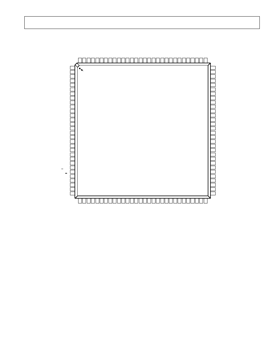
ADV611/ADV612
45
REV. 0
ADV611/ADV612 PIN CONFIGURATION
11
10
16
15
14
13
18
17
20
19
22
21
12
24
23
26
25
28
27
30
29
5
4
3
2
7
6
9
8
1
32
33
35
36
38
39
40
41
42
43
44
45
46
47
48
49
50
31
37
60
59
58
57
54
53
52
51
56
55
34
PIN 1
IDENTIFIER
TOP VIEW
(Not to Scale)
86
87
89
84
85
82
83
81
90
80
88
75
76
77
78
73
74
72
70
71
79
69
67
68
65
66
63
64
61
62
11
2
11
3
11
4
115
116
11
7
11
8
11
9
12
0
111
10
3
11
0
10
9
10
8
10
7
10
6
10
4
10
2
10
1
10
0
99
98
97
96
95
94
93
92
91
10
5
DATA
5
DATA
6
DATA
7
DATA
8
DATA
9
DATA
1
0
DATA
1
1
DATA
1
2
DATA
1
3
DATA
1
4
DATA
1
5
GND
GND
DATA
1
6
DATA
1
7
DATA
1
8
DATA
1
9
VDD
DATA
2
0
DATA
2
1
DATA
2
2
DATA
2
3
DATA
2
4
DATA
2
5
DATA
2
6
DATA
2
7
DATA
2
8
DATA
2
9
DATA
3
0
DATA
3
1
DADR7
DADR6
DADR5
DADR4
DADR3
DADR2
DADR1
DADR0
GND
RAS
CAS
WE
VDD
VDD
DDAT15
DDAT14
DDAT13
DDAT12
DDAT11
DDAT10
DDAT9
DDAT8
DDAT7
DDAT6
DDAT5
DDAT4
DDAT3
DDAT2
DDAT1
DDAT0
GND
NC*
NC*
VDATA0
VDATA1
VDATA2
VDATA3
VDD
GND
VDATA4
VDATA5
VDATA6
VDATA7
VCLKO
ENC
GND
STALL
VDD
GND
VDD
GND
VDD
GND
VSYNC
HSYNC
FIELD
GND
VCLK
XTAL
VDD
DATA4
DATA3
DATA2
DATA1
DATA0
VDD
GND
RD
WR
CS
ADR1
ADR0
GND
BE2
BE3
BE0
BE1
GND
RESET
VDD
ACK
VDD
GND
HIRQ
LCODE
FIFO SRQ
STATS R
VDD
GND
GND
VDD
DADR8
*APPLY A 10k PULL DOWN RESISTOR TO THIS PIN
ADV611/ADV612
LQFP
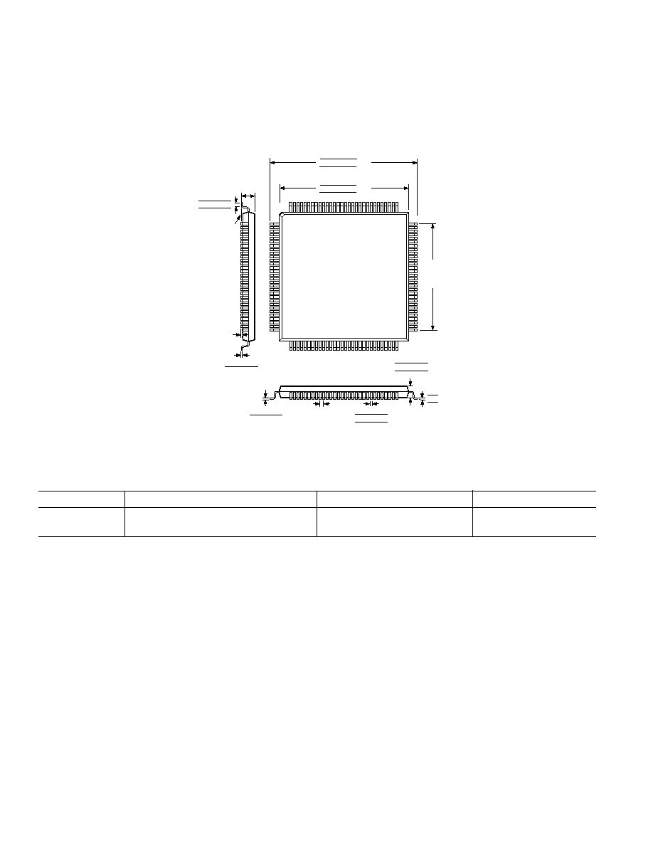
ADV611/ADV612
46
REV. 0
120-Lead LQFP
(ST-120)
TOP VIEW
(PINS DOWN)
1
30
31
61
60
90
120
91
0.457
(11.6)
BSC
SQ
0.638 (16.20)
0.630 (16.00) SQ
0.622 (15.80)
0.559 (14.20)
0.551 (14.00) SQ
0.543 (13.80)
SEATING
PLANE
0.063 (1.60)
MAX
COPLANARITY
0.003 (0.08)
MAX
0.006 (0.15)
0.002 (0.05)
0.030 (0.75)
0.024 (0.60)
0.020 (0.50)
0.016 (0.40)
BSC
*
7
3.5
0
0.008 (0.20)
0.004 (0.09)
0.009 (0.23)
0.007 (0.18)
0.005 (0.13)
0.057 (1.45)
0.055 (1.40)
0.053 (1.35)
* THE ACTUAL POSITION OF EACH LEAD IS WITHIN 0.07 mm
LATERAL TO THE PINS TRUE POSITION.
CENTER FIGURES ARE TYPICAL UNLESS OTHERWISE NOTED
ORDERING GUIDE
Part Number
Ambient Temperature Range
1
Package Description
Package Options
2
ADV611JST
0
°
C to +70
°
C
120-Lead LQFP
ST-120
ADV612BST
3
25
°
C to +85
°
C
120-Lead LQFP
ST-120
NOTES
1
J = Commercial temperature range (0
°
C to +70
°
C).
2
ST = Plastic Thin Quad Flatpack.
3
B = Standard Industrial Temperature Range (25
°
C to +85
°
C).
OUTLINE DIMENSIONS
Dimensions shown in inches and (mm).
C339931/99
PRINTED IN U.S.A.