ADV7121/ADV7122 CMOS 80MHz, Triple 10-Bit Video DACs
REV. B
Information furnished by Analog Devices is believed to be accurate and
reliable. However, no responsibility is assumed by Analog Devices for its
use, nor for any infringements of patents or other rights of third parties
which may result from its use. No license is granted by implication or
otherwise under any patent or patent rights of Analog Devices.
a
CMOS
80 MHz, Triple 10-Bit Video DACs
ADV7121/ADV7122
© Analog Devices, Inc., 1996
One Technology Way, P.O. Box 9106, Norwood, MA 02062-9106, U.S.A.
Tel: 617/329-4700
Fax: 617/326-8703
ADV7121 FUNCTIONAL BLOCK DIAGRAM
PIXEL
INPUT
PORT
IOR
IOG
IOB
R0
R9
CLOCK
10
ADV7121
V
REF
G0
G9
10
B0
B9
10
FS
ADJUST
10
10
10
V
AA
REFERENCE
AMPLIFIER
COMP
DAC
DAC
RED
REGISTER
BLUE
REGISTER
GREEN
REGISTER
DAC
GND
ADV7122 FUNCTIONAL BLOCK DIAGRAM
PIXEL
INPUT
PORT
IOR
IOG
IOB
R0
R9
CLOCK
10
SYNC
ADV7122
GND
G0
G9
10
B0
B9
10
BLANK
FS
ADJUST
10
10
10
V
AA
REFERENCE
AMPLIFIER
COMP
DAC
DAC
RED
REGISTER
BLUE
REGISTER
CONTROL
REGISTER
GREEN
REGISTER
DAC
SYNC
CONTROL
V
REF
FEATURES
80 MHz Pipelined Operation
Triple 10-Bit D/A Converters
RS-343A/RS-170 Compatible Outputs
TTL Compatible Inputs
+5 V CMOS Monolithic Construction
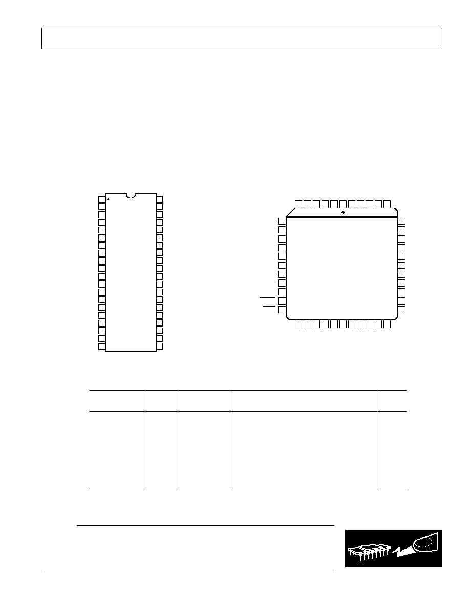
40-Pin DIP Package (ADV7121)
44-Pin PLCC Package (ADV7122)
48-Lead TQFP (ADV7122)
APPLICATIONS
High Definition Television (HDTV)
High Resolution Color Graphics
CAE/CAD/CAM Applications
Image Processing
Instrumentation
Video Signal Reconstruction
Direct Digital Synthesis (DDS)
I/Q Modulation
SPEED GRADES
80 MHz
50 MHz
30 MHz
ADV is a registered trademark of Analog Devices, Inc.
*Speed grades up to 140 MHz are also available on special request.
Please contact Analog Devices or its representatives for details.
GENERAL DESCRIPTION
The ADV7121/ADV7122 (ADV
®
) is a video speed, digital-to-
analog converter on a single monolithic chip. The part is specifi-
cally designed for high resolution color graphics and video
systems including high definition television (HDTV). It is also
ideal for any application requiring a low cost, high speed DAC
function especially in communications. It consists of three, high
speed, 10-bit, video D/A converters (RGB), a standard TTL input
interface and high impedance, analog output, current sources.
The ADV7121/ADV7122 has three separate, 10-bit, pixel input
ports, one each for red, green and blue video data. A single +5 V
power supply, an external 1.23 V reference and pixel clock input is
all that is required to make the part operational. The ADV7122
has additional video control signals, composite SYNC and BLANK.
The ADV7121/ADV7122 is capable of generating RGB video
output signals which are compatible with RS-343A, RS-170 and
most proposed production system HDTV video standards, in-
cluding SMPTE 240M.
The ADV7121/ADV7122 is fabricated in a +5 V CMOS pro-
cess. Its monolithic CMOS construction ensures greater func-
tionality with low power dissipation. The ADV7121 is packaged
in a 0.6", 40-pin plastic DIP package. The ADV7122 is pack-
aged in a 44-pin plastic leaded (J-lead) chip carrier, PLCC,
and 48-lead thin quad flatpack (TQFP).
PRODUCT HIGHLIGHTS
1. Fast video refresh rate, 80 MHz.
2. Guaranteed monotonic to 10 bits. Ten bits of resolution al-
lows for implementation of linearization functions such as
gamma correction and contrast enhancement.
3. Compatible with a wide variety of high resolution color
graphics systems including RS-343A/RS-170 and the pro-
posed SMPTE 240M standard for HDTV.
REV. B
2
ADV7121SPECIFICATIONS
Parameter
K Version
Units
Test Conditions/Comments
STATIC PERFORMANCE
Resolution (Each DAC)
10
Bits
Accuracy (Each DAC)
Integral Nonlinearity, INL
±
2
LSB max
Differential Nonlinearity, DNL
±
1
LSB max
Guaranteed Monotonic
Gray Scale Error
±
5
% Gray Scale max
Max Gray Scale Current = (V
REF
* 7,969/R
SET
) mA
Coding
Binary
DIGITAL INPUTS
Input High Voltage, V
INH
2
V min
Input Low Voltage, V
INL
0.8
V max
Input Current, I
IN
±
1
µ
A max
V
IN
= 0.4 V or 2.4 V
Input Capacitance, C
IN
2
10
pF max
ANALOG OUTPUTS
Gray Scale Current Range
15
mA min
22
mA max
Output Current
White Level
16.74
mA min
Typically 17.62 mA
18.50
mA max
Black Level
0
µ
A min
Typically 5
µ
A
50
µ
A max
LSB Size
17.28
µ
A typ
DAC to DAC Matching
5
% max
Typically 2%
Output Compliance, V
OC
1
V min
+1.4
V max
Output Impedance, R
OUT
2
100
k
typ
Output Capacitance, C
OUT
2
30
pF max
I
OUT
= 0 mA
VOLTAGE REFERENCE
Voltage Reference Range, V
REF
1.14/1.26
V min/V max
V
REF
= 1.235 V for Specified Performance
Input Current, I
VREF
5
mA typ
POWER REQUIREMENTS
V
AA
5
V nom
I
AA
125
mA max
Typically 80 mA: 80 MHz Parts
100
mA max
Typically 70 mA: 50 MHz & 35 MHz Parts
Power Supply Rejection Ratio
2
0.5
%/% max
Typically 0.12 %/%: f = 1 kHz, COMP = 0.1
µ
F
Power Dissipation
625
mW max
Typically 400 mW: 80 MHz Parts
500
mW max
Typically 350 mW: 50 MHz & 35 MHz Parts
DYNAMIC PERFORMANCE
Glitch Impulse
2, 3
50
pV secs typ
DAC Noise
2, 3, 4
200
pV secs typ
Analog Output Skew
2
ns max
Typically 1 ns
NOTES
1
Temperature range (T
MIN
to T
MAX
): 0
°
C to +70
°
C.
2
Sample tested at +25
°
C to ensure compliance.
3
TTL input values are 0 to 3 volts, with input rise/fall times
3 ns, measured between the 10% and 90% points. Timing reference points at 50% for inputs and
outputs. See timing notes in Figure 1.
4
This includes effects due to clock and data feedthrough as well as RGB analog crosstalk.
Specifications subject to change without notice.
(V
AA
= +5 V 5%; V
REF
= +1.235 V; R
L
= 3.75 , C
L
= 10 pF; R
SET
= 560
. All
Specifications T
MIN
to T
MAX
1
unless otherwise noted.)
ADV7121/ADV7122
3
REV. B
Parameter
K Version
Units
Test Conditions/Comments
STATIC PERFORMANCE
Resolution (Each DAC)
10
Bits
Accuracy (Each DAC)
Integral Nonlinearity, INL
±
2
LSB max
Differential Nonlinearity, DNL
±
1
LSB max
Guaranteed Monotonic
Gray Scale Error
±
5
% Gray Scale max
Max Gray Scale Current: IOG = (V
REF
*12.082/R
SET
) mA
Max Gray Scale Current:
IOR, IOB = (V
REF
*8,627/R
SET
) mA
Coding
Binary
DIGITAL INPUTS
Input High Voltage, V
INH
2
V min
Input Low Voltage, V
INL
0.8
V max
Input Current, I
IN
±
1
µ
A max
V
IN
= 0.4 V or 2.4 V
Input Capacitance, C
IN
2
10
pF max
ANALOG OUTPUTS
Gray Scale Current Range
15
mA min
22
mA max
Output Current
White Level Relative to Blank
17.69
mA min
Typically 19.05 mA
20.40
mA max
White Level Relative to Black
16.74
mA min
Typically 17.62 mA
18.50
mA max
Black Level Relative to Blank
0 95
mA min
Typically 1.44 mA
1.90
mA max
Black Level on IOR, IOB
0
µ
A min
Typically 5
µ
A
50
µ
A max
Black Level on IOG
6.29
mA min
Typically 7.62 mA
9.5
mA max
Sync Level on IOG
0
µ
A min
Typically 5
µ
A
50
µ
A max
LSB Size
17.28
µ
A typ
DAC to DAC Matching
5
% max
Typically 2%
Output Compliance, V
OC
1
V min
+1.4
V max
Output Impedance, R
OUT
2
100
k
typ
Output Capacitance, C
OUT
2
30
pF max
I
OUT
= 0 mA
VOLTAGE REFERENCE
Voltage Reference Range, V
REF
1.14/1.26
V min/V max
V
REF
= 1.235 V for Specified Performance
Input Current, I
VREF
5
mA typ
POWER REQUIREMENTS
V
AA
5
V nom
I
AA
125
mA max
Typically 80 mA: 80 MHz Parts
100
mA max
Typically 70 mA: 50 MHz & 35 MHz Parts
Power Supply Rejection Ratio
2
0.5
%/% max
Typically 0.12%/%: f = 1 kHz, COMP = 0.01
µ
F
Power Dissipation
625
mW max
Typically 400 mW: 80 MHz Parts
500
mW max
Typically 350 mW: 50 MHz & 35 MHz Parts
DYNAMIC PERFORMANCE
Glitch Impulse
2, 3
50
pV secs typ
DAC Noise
2, 3, 4
200
pV secs typ
Analog Output Skew
2
ns max
Typically 1 ns
NOTES
1
Temperature range (T
MIN
to T
MAX
) 0
°
C to +70
°
C.
2
Sample tested at +25
°
C to ensure compliance.
3
TTL input values are 0 to 3 volts, with input rise/fall times
3 ns, measured between the 10% and 90% points. Timing reference points at 50% for inputs and
outputs. See timing notes in Figure 1.
4
This includes effects due to clock and data feedthrough as well as RGB analog crosstalk.
Specifications subject to change without notice
ADV7122SPECIFICATIONS
(V
AA
= +5 V 5%; V
REF
= +1.235 V; R
L
= 37.5
, C
L
= 10 pF; R
SET
= 560
. All
Specifications T
MIN
to T
MAX
1
unless otherwise noted.)
ADV7121/ADV7122
4
REV. B
TIMING CHARACTERISTICS
1
(V
AA
= +5 V 5%; V
REF
= +1.235 V; R
L
= 37.5 , C
L
= 10 pF; R
SET
= 560
.
All Specifications T
MIN
to T
MAX
2
unless otherwise noted.)
Parameter
80 MHz Version
50 MHz Version
30 MHz Version
Units
Conditions/Comments
fmax
80
50
30
MHz max
Clock Rate
t
1
3
6
8
ns min
Data & Control Setup Time
t
2
2
2
2
ns min
Data & Control Hold Time
t
3
12.5
20
33.3
ns min
Clock Cycle Time
t
4
4
7
9
ns min
Clock Pulse Width High Time
t
5
4
7
9
ns min
Clock Pulse Width Low Time
t
6
30
30
30
ns max
Analog Output Delay
20
20
20
ns typ
t
7
3
3
3
ns max
Analog Output Rise/Fall Time
t
8
3
12
15
15
ns typ
Analog Output Transition Time
NOTES
1
TTL input values are 0 to 3 volts, with input rise/fall times
3 ns, measured between the 10% and 90% points. Timing reference points at 50% for inputs and
outputs. See timing notes in Figure 1.
2
Temperature range (T
MIN
to T
MAX
): 0
°
C to +70
°
C.
3
Sample tested at +25
°
C to ensure compliance.
Specifications subject to change without notice.
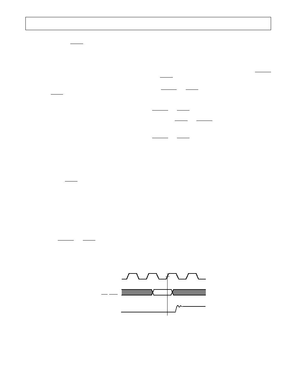
CLOCK
DATA
DIGITAL INPUTS
(R0R9, G0G9, B0B9;
SYNC, BLANK)
t
4
t
5
t
6
t
2
t
1
t
8
t
7
ANALOG OUTPUTS
(IOR, IOG, IOB)
t
3
1. OUTPUT DELAY (t
6
) MEASURED FROM THE 50% POINT OF THE
RISING EDGE OF THE CLOCK TO THE 50% POINT OF
FULL-SCALE TRANSITION.
2. TRANSITION TIME (t
8
) MEASURED FROM THE 50% POINT OF
FULL-SCALE TRANSITION TO WITHIN 2% OF THE FINAL OUTPUT
VALUE.
3. OUTPUT RISE/FALL TIME (t
7
) MEASURED BETWEEN THE 10%
AND 90% POINTS OF FULL-SCALE TRANSITION.
4 SYNC AND BLANK DIGITAL INPUTS ARE NOT PROVIDED ON
NOTES
Figure 1. Video Input/Output Timing
RECOMMENDED OPERATING CONDITIONS
Parameter
Symbol
Min
Typ
Max
Units
Power Supply
V
AA
4.75
5.00
5.25
Volts
Ambient Operating
Temperature
T
A
0
+70
°
C
Output Load
R
L
37.5
Reference Voltage
V
REF
1.14
1.235
1.26
Volts
ADV7121/ADV7122
5
REV. B
ABSOLUTE MAXIMUM RATINGS
1
V
AA
to GND . . . . . . . . . . . . . . . . . . . . . . . . . . . . . . . . . . +7 V
Voltage on Any Digital Pin . . . . . GND 0.5 V to V
AA
+ 0.5 V
Ambient Operating Temperature (T
A
) . . . . . . . . 0
°
C to +70
°
C
Storage Temperature (T
S
) . . . . . . . . . . . . . . 65
°
C to +150
°
C
Junction Temperature (T
J
) . . . . . . . . . . . . . . . . . . . . +150
°
C
Soldering Temperature (5 secs) . . . . . . . . . . . . . . . . . . . 220
°
C
Vapor Phase Soldering (1 minute) . . . . . . . . . . . . . . . . . 220
°
C
IOR, IOB, IOG to GND
2
. . . . . . . . . . . . . . . . . . . 0 V to V
AA
NOTES
1
Stresses above those listed under "Absolute Maximum Ratings" may cause
permanent damage to the device. This is a stress rating only and functional
operation of the device at these or any other conditions above those listed in the
operational sections of this specification is not implied. Exposure to absolute
maximum rating conditions for extended periods may affect device reliability.
2
Analog output short circuit to any power supply or common can be of an indefinite
duration.
PIN CONFIGURATIONS
DIP (N-40A) Package
1
2
3
4
5
6
7
8
9
10
11
12
13
14
28
27
26
25
24
23
22
21
40
39
38
37
36
35
34
33
32
31
30
29
15
16
17
18
19
20
TOP VIEW
(Not to Scale)
ADV7121 DIP
R5
R4
R3
R2
R1
R0
IOB
IOG
V
AA
GND
FS ADJUST
IOR
CLOCK
B9
B8
B7
B6
B5
V
REF
COMP
R6
R7
R8
R9
G0
G1
G2
G3
G4
G6
G7
G8
G9
B0
B1
B2
B3
B4
G5
V
AA
PLCC (P-44A) Package
4
3
2
1
28
27
26
5
6
7
8
9
10
11
12
13
14
15
16
17
18 19 20 21 22 23 24 25
ADV7122 PLCC
TOP VIEW
(Not to Scale)
44 43 42 41 40
39
38
37
36
35
34
33
32
31
30
29
B2
B0
B3
R3
B1
G4
G5
G6
G7
BLANK
SYNC
CLOCK
R0
R1
R2
G8
G9
G1
G2
G3
COMP
FS ADJUST
GND
GND
IOG
IOR
IOB
B9
R5
R4
G0
R8
R7
R6
R9
V
AA
V
AA
V
AA
V
REF
B6
B4
B7
B5
B8
WARNING!
ESD SENSITIVE DEVICE
CAUTION
ESD (electrostatic discharge) sensitive device. Electrostatic charges as high as 4000 V readily
accumulate on the human body and test equipment and can discharge without detection.
Although the ADV7121/ADV7122 feature proprietary ESD protection circuitry, permanent
damage may occur on devices subjected to high energy electrostatic discharges. Therefore, p roper
ESD precautions are recommended to avoid performance degradation or loss of fu nctionality.
ORDERING GUIDE
Temperature
Package
Package
Model
Speed
Range
*
Description
Option
ADV7121KN80
80 MHz
0
°
C to +70
°
C
40-Pin Plastic DIP
N-40A
ADV7121KN50
50 MHz
0
°
C to +70
°
C
40-Pin Plastic DIP
N-40A
ADV7121KN30
30 MHz
0
°
C to +70
°
C
40-Pin Plastic DIP
N-40A
ADV7122KP80
80 MHz
0
°
C to +70
°
C
44-Lead Plastic Leaded Chip Carrier (PLCC) P-44A
ADV7122KP50
50 MHz
0
°
C to +70
°
C
44-Lead Plastic Leaded Chip Carrier (PLCC) P-44A
ADV7122KP30
30 MHz
0
°
C to +70
°
C
44-Lead Plastic Leaded Chip Carrier (PLCC) P-44A
ADV7122KST50 50 MHz
0
°
C to +70
°
C
48-Lead Thin Quad Flatpack (TQFP)
ST-48
ADV7122KST30 30 MHz
0
°
C to +70
°
C
48-Lead Thin Quad Flatpack (TQFP)
ST-48
*Industrial Temperature range (40
°
C to +85
°
C) parts are also available to special ranges. Please contact your local Analog Devices
representative.
ADV7121/ADV7122
6
REV. B
PIN FUNCTION DESCRIPTION
Pin
Mnemonic
Function
BLANK
*
Composite blank control input (TTL compatible). A logic zero on this control input drives the analog outputs,
IOR, IOB and IOG, to the blanking level. The BLANK signal is latched on the rising edge of CLOCK. While
BLANK
is a logical zero, the R0R9, G0G9 and R0R9 pixel inputs are ignored.
SYNC
*
Composite sync control input (TTL compatible). A logical zero on the SYNC input switches off a 40 IRE
current source. This is internally connected to the IOG analog output. SYNC does not override any other
control or data input, therefore, it should only be asserted during the blanking interval. SYNC is latched on the
rising edge of CLOCK.
If sync information is not required on the green channel, the SYNC input should be tied to logical zero.
CLOCK
Clock input (TTL compatible). The rising edge of CLOCK latches the R0R9, G0G9, B0B9, SYNC and
BLANK
pixel and control inputs. It is typically the pixel clock rate of the video system. CLOCK should be
driven by a dedicated TTL buffer.
R0R9,
Red, green and blue pixel data inputs (TTL compatible). Pixel data is latched on the rising edge of CLOCK.
G0G9,
R0, G0 and B0 are the least significant data bits. Unused pixel data inputs should be connected to either the
B0B9
regular PCB power or ground plane.
IOR, IOG, IOB Red, green, and blue current outputs. These high impedance current sources are capable of directly driving a
doubly terminated 75
coaxial cable. All three current outputs should have similar output loads whether or not
they are all being used.
FS ADJUST
Full-scale adjust control. A resistor (R
SET
) connected between this pin and GND, controls the magnitude of the
full-scale video signal. Note that the IRE relationships are maintained, regardless of the full-scale output current.
The relationship between R
SET
and the full-scale output current on IOG (assuming I
SYNC
is connected to IOG)
is given by:
R
SET
(
)
= 12,082
×
V
REF
(V)/IOG (mA)
The relationship between R
SET
and the full-scale output current on IOR, IOG and IOB is given by:
IOG* (mA)
= 12,082
×
V
REF
(V)/R
SET
(
) (SYNC being asserted)
IOR, IOB (mA)
= 8,628
×
V
REF
(V)/R
SET
(
)
The equation for IOG will be the same as that for IOR and IOB when SYNC is not being used, i.e., SYNC
tied permanently low. For the ADV7121, all three analog output currents are as described by:
IOR, IOG, IOB (mA)
= 7,969
×
V
REF
(V)/R
SET
(
)
COMP
Compensation pin. This is a compensation pin for the internal reference amplifier. A 0.1
µ
F ceramic capacitor
must be connected between COMP and V
AA
.
V
REF
Voltage reference input. An external 1.23 V voltage reference must be connected to this pin. The use of an
external resistor divider network is not recommended. A 0.1
µ
F decoupling ceramic capacitor should be
connected between V
REF
and V
AA
.
V
AA
Analog power supply (5 V
±
5%). All V
AA
pins on the ADV7121/ADV7122 must be connected.
GND
Ground. All GND pins must be connected.
*SYNC and BLANK functions are not provided on the ADV7121.
ADV7121/ADV7122
7
REV. B
TERMINOLOGY
Blanking Level
The level separating the SYNC portion from the video portion
of the waveform. Usually referred to as the front porch or back
porch. At 0 IRE units, it is the level which will shut off the pic-
ture tube, resulting in the blackest possible picture.
Color Video (RGB)
This usually refers to the technique of combining the three pri-
mary colors of red, green and blue to produce color pictures
within the usual spectrum. In RGB monitors, three DACs are
required, one for each color.
Sync Signal (SYNC)
The position of the composite video signal which synchronizes
the scanning process.
Gray Scale
The discrete levels of video signal between reference black and
reference white levels. A 10-bit DAC contains 1024 different
levels, while an 8-bit DAC contains 256.
Raster Scan
The most basic method of sweeping a CRT one line at a time to
generate and display images.
Reference Black Level
The maximum negative polarity amplitude of the video signal.
Reference White Level
The maximum positive polarity amplitude of the video signal.
Sync Level
The peak level of the SYNC signal.
Video Signal
That portion of the composite video signal which varies in gray
scale levels between reference white and reference black. Also
referred to as the picture signal, this is the portion which may be
visually observed.
CIRCUIT DESCRIPTION & OPERATION
The ADV7121/ADV7122 contains three 10-bit D/A converters,
with three input channels, each containing a 10-bit register.
Also integrated on board the part is a reference amplifier. CRT
control functions BLANK and SYNC are integrated on board
the ADV7122.
Digital Inputs
Thirty bits of pixel data (color information) R0R9, G0G9 and
B0B9 are latched into the device on the rising edge of each
clock cycle. This data is presented to the three 10-bit DACs and
is then converted to three analog (RGB) output waveforms. See
Figure 2.
The ADV7122 has two additional control signals, which are
latched to the analog video outputs in a similar fashion. BLANK
and SYNC are each latched on the rising edge of CLOCK to
maintain synchronization with the pixel data stream.
The BLANK and SYNC functions allow for the encoding of
these video synchronization signals onto the RGB video output.
This is done by adding appropriately weighted current sources
to the analog outputs, as determined by the logic levels on the
BLANK
and SYNC digital inputs. Figure 3 shows the analog
output, RGB video waveform of the ADV7121/ADV7122. The
influence of SYNC and BLANK on the analog video waveform
is illustrated.
Table I details the resultant effect on the analog outputs of
BLANK
and SYNC.
All these digital inputs are specified to accept TTL logic levels.
Clock Input
The CLOCK input of the ADV7121/ADV7122 is typically the
pixel clock rate of the system. It is also known as the dot rate.
The dot rate, and hence the required CLOCK frequency, will be
determined by the on-screen resolution, according to the follow-
ing equation:
Dot Rate = (Horiz Res)
×
(Vert Res)
×
(Refresh Rate)/
(Retrace Factor)
Horiz Res
= Number of Pixels/Line.
Vert Res
= Number of Lines/Frame.
Refresh Rate
= Horizontal Scan Rate. This is the rate at
which the screen must be refreshed, typ-
ically 60 Hz for a noninterlaced system or
30 Hz for an interlaced system.
Retrace Factor
= Total Blank Time Factor. This takes into
account that the display is blanked for a
certain fraction of the total duration of
each frame (e.g., 0.8).
CLOCK
DATA
DIGITAL INPUTS
(R0R9, G0G9, B0B9;
SYNC, BLANK)
ANALOG OUTPUTS
(IOR, IOG, IOB)
Figure 2. Video Data Input/Output
ADV7121/ADV7122
8
REV. B
If we, therefore, have a graphics system with a 1024
×
1024
resolution, a noninterlaced 60 Hz refresh rate and a retrace fac-
tor of 0.8, then:
Dot Rate =
1024
×
1024
×
60/0.8
= 78.6
MHz
The required CLOCK frequency is thus 78.6 MHz.
All video data and control inputs are latched into the ADV7121/
ADV7122 on the rising edge of CLOCK, as previously de-
scribed in the "Digital Inputs" section. It is recommended that
the CLOCK input to the ADV7121/ADV7122 be driven by a
TTL buffer (e.g., 74F244).
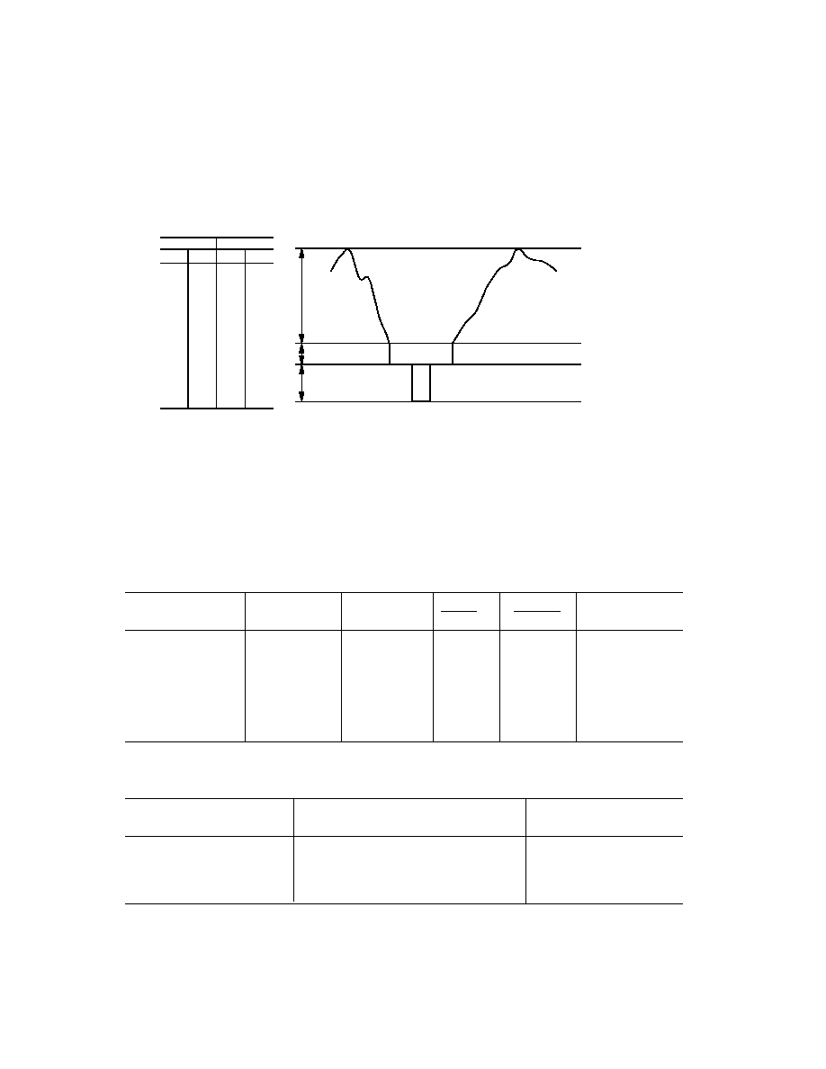
92.5 IRE
7.5 IRE
40 IRE
WHITE LEVEL
BLACK LEVEL
BLANK LEVEL
SYNC LEVEL
19.05 0.714 26.67 1.000
1.44 0.054 9.05 0.340
0 0 7.62 0.286
0
0
mA V mA V
RED, BLUE GREEN
NOTES
1. OUTPUTS CONNECTED TO A DOUBLY TERMINATED 75
LOAD.
2. V
REF
= 1.235V, R
SET
= 560
.
3. RS343A LEVELS AND TOLERANCES ASSUMED ON ALL
LEVELS.
Figure 3. RGB Video Output Waveform
Table Ia. Video Output Truth Table for the ADV7122
IOG
IOR, IOB
DAC
Description
(mA)*
(mA)
SYNC
BLANK
Input Data
WHITE LEVEL
26.67
19.05
1
1
3FFH
VIDEO
video + 9.05
video + 1.44
1
1
data
VIDEO to BLANK
video + 1.44
video + 1.44
0
1
data
BLACK LEVEL
9.05
1.44
1
1
00H
BLACK to BLANK
1.44
1.44
0
1
00H
BLANK LEVEL
7.62
0
1
0
xxH
SYNC LEVEL
0
0
0
0
xxH
*Typical with full-scale IOG = 26.67 mA. V
REF
= 1.235 V, R
SET
= 560
, I
SYNC
connected to IOG.
Table Ib. Video Output Truth Table for the ADV7121
IOR, IOG, IOB
DAC
Description
(mA)*
Input Data
WHITE LEVEL
17.62
3FF
VIDEO
video
data
VIDEO to BLACK
video
data
BLACK LEVEL
0
00H
*Typical with full scale = 17.62 mA. V
REF
= 1.235 V, R
SET
= 560
.
ADV7121/ADV7122
9
REV. B
Video Synchronization & Control
The ADV7122 has a single composite sync (SYNC) input con-
trol. Many graphics processors and CRT controllers have the
ability of generating horizontal sync (HSYNC), vertical sync
(VSYNC) and composite SYNC.
In a graphics system which does not automatically generate a
composite SYNC signal, the inclusion of some additional logic
circuitry will enable the generation of a composite SYNC signal.
The sync current is internally connected directly to the IOG
output, thus encoding video synchronization information onto
the green video channel. If it is not required to encode sync in-
formation onto the ADV7122, the SYNC input should be tied
to logic low.
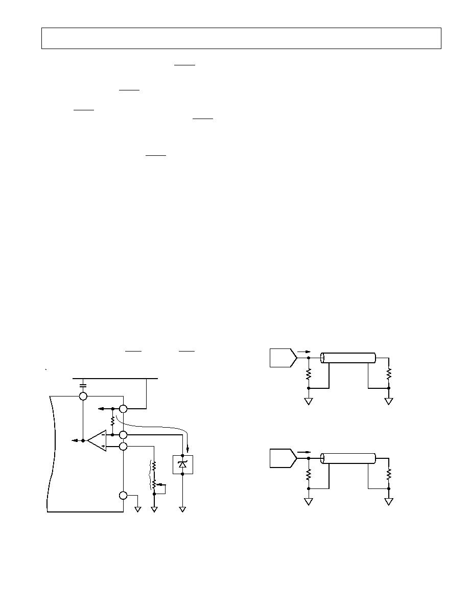
Reference Input
An external 1.23 V voltage reference is required to drive the
ADV7121/ADV7122. The AD589 from Analog Devices is an
ideal choice of reference. It is a two-terminal, low cost, tempera-
ture compensated bandgap voltage reference which provides a
fixed 1.23 V output voltage for input currents between 50
µ
A
and 5 mA. Figure 4 shows a typical reference circuit connection
diagram. The voltage reference gets its current drive from the
ADV7121/ADV7122's V
AA
through an onboard 1 k
resistor to
the V
REF
pin. A 0.1
µ
F ceramic capacitor is required between
the COMP pin and V
AA
. This is necessary so as to provide com-
pensation for the internal reference amplifier.
A resistance R
SET
connected between FS ADJUST and GND
determines the amplitude of the output video level according to
Equations 1 and 2 for the ADV7122 and Equation 3 for the
ADV7121:
IOG* (mA) = 12,082
×
V
REF
(V)/R
SET
(
) (1)
IOR, IOB (mA) = 8,628
×
V
REF
(V)/R
SET
(
)
(2)
IOR, IOG, IOB (mA) = 7,969
×
V
REF
(V)/R
SET
(
)
(3)
*Only applies to the ADV7122 when SYNC is being used. If SYNC is not being
encoded onto the green channel, then Equation 1 will be similar to Equation 2.
TO DACs
V
AA
V
REF
GND
1k
FS ADJUST
R
SET
560
500
100
ANALOG POWER PLANE
COMP
0.01
µ
F
5V
+
I
REF
5mA
AD589
(1.235V
VOLTAGE
REFERENCE)
ADV7121/ADV7122*
*ADDITIONAL CIRCUITRY, INCLUDING
DECOUPLING COMPONENTS,
EXCLUDED FOR CLARIITY
Figure 4. Reference Circuit
Using a variable value of R
SET
, as shown in Figure 4, allows for
accurate adjustment of the analog output video levels. Use of a
fixed 560
R
SET
resistor yields the analog output levels as quoted
in the specification page. These values typically correspond to
the RS-343A video waveform values as shown in Figure 3.
D/A Converters
The ADV7121/ADV7122 contains three matched 10-bit D/A
converters. The DACs are designed using an advanced, high
speed, segmented architecture. The bit currents corresponding
to each digital input are routed to either the analog output (bit
= "1") or GND (bit = "0") by a sophisticated decoding scheme.
As all this circuitry is on one monolithic device, matching be-
tween the three DACs is optimized. As well as matching, the
use of identical current sources in a monolithic design guaran-
tees monotonicity and low glitch. The onboard operational am-
plifier stabilizes the full-scale output current against temperature
and power supply variations.
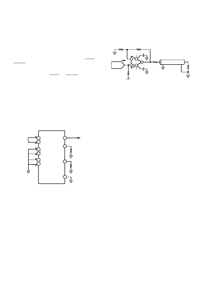
Analog Outputs
The ADV7121/ADV7122 has three analog outputs, correspond-
ing to the red, green and blue video signals.
The red, green and blue analog outputs of the ADV7121/
ADV7122 are high impedance current sources. Each one of
these three RGB current outputs is capable of directly driving a
37.5
load, such as a doubly terminated 75
coaxial cable.
Figure 5a shows the required configuration for each of the three
RGB outputs connected into a doubly terminated 75
load.
This arrangement will develop RS-343A video output voltage
levels across a 75
monitor.
A suggested method of driving RS-170 video levels into a 75
monitor is shown in Figure 5b. The output current levels of the
DACs remain unchanged, but the source termination resistance,
Z
S
, on each of the three DACs is increased from 75
to 150
.
DACs
IOR, IOG, IOB
Z
O
= 75
(CABLE)
Z
S
= 75
(SOURCE
TERMINATION)
TERMINATION REPEATED THREE TIMES
FOR RED, GREEN AND BLUE DACs
Z
L
= 75
(MONITOR)
Figure 5a. Analog Output Termination for RS-343A
DACs
IOR, IOG, IOB
Z
O
= 75
(CABLE)
Z
S
= 150
(SOURCE
TERMINATION)
TERMINATION REPEATED THREE TIMES
FOR RED, GREEN AND BLUE DACs
Z
L
= 75
(MONITOR)
Figure 5b. Analog Output Termination for RS-170
ADV7121/ADV7122
10
REV. B
More detailed information regarding load terminations for vari-
ous output configurations, including RS-343A and RS-170, is
available in an Application Note entitled "Video Formats &
Required Load Terminations" available from Analog Devices,
publication no. E1228151/89.
Figure 3 shows the video waveforms associated with the three
RGB outputs driving the doubly terminated 75
load of Fig-
ure 5a. As well as the gray scale levels, Black Level to White
Level, the diagram also shows the contributions of SYNC and
BLANK
for the ADV7122. These control inputs add appropri-
ately weighted currents to the analog outputs, producing the
specific output level requirements for video applications.
Table Ia. details how the SYNC and BLANK inputs modify
the output levels.
Gray Scale Operation
The ADV7121/ADV7122 can be used for stand-alone, gray
scale (monochrome) or composite video applications (i.e., only
one channel used for video information). Any one of the three
channels, RED, GREEN or BLUE can be used to input the
digital video data. The two unused video data channels should
be tied to logical zero. The unused analog outputs should be
terminated with the same load as that for the used channel. In
other words, if the red channel is used and IOR is terminated
with a doubly terminated 75
load (37.5
), IOB and IOG
should be terminated with 37.5
resistors. See Figure 6.
GND
ADV7121/ADV7122
R0
R9
G0
G9
B0
B9
VIDEO
INPUT
DOUBLY
TERMINATED
75
LOAD
IOR
IOG
IOB
37.5
37.5
Figure 6. Input and Output Connections for Stand-Alone
Gray Scale or Composite Video
Video Output Buffers
The ADV7121/ADV7122 is specified to drive transmission line
loads, which is what most monitors are rated as. The analog
output configurations to drive such loads are described in the
Analog Interface section and illustrated in Figure 5. However,
in some applications it may be required to drive long "transmis-
sion line" cable lengths. Cable lengths greater than 10 meters
can attenuate and distort high frequency analog output pulses.
The inclusion of output buffers will compensate for some cable
distortion. Buffers with large full power bandwidths and gains
between 2 and 4 will be required. These buffers will also need
to be able to supply sufficient current over the complete output
voltage swing. Analog Devices produces a range of suitable op
amps for such applications. These include the AD84x series of
monolithic op amps. In very high frequency applications (80 MHz),
the AD9617 is recommended. More information on line driver
buffering circuits is given in the relevant op amp data sheets.
Use of buffer amplifiers also allows implementation of other
video standards besides RS-343A and RS-170. Altering the gain
components of the buffer circuit will result in any desired video
level.
DACs
Z
O
= 75
(CABLE)
Z
S
= 75
(SOURCE
TERMINATION)
AD848
+V
S
0.1
µ
F
0.1
µ
F
IOR, IOG, IOB
75
2
7
6
4
3
Z
1
Z
L
= 75
(MONITOR)
Z
1
Z
2
GAIN (G) = 1+
V
S
Z
2
Figure 7. AD848 As an Output Buffer
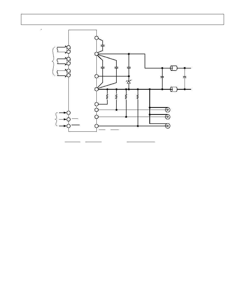
PC Board Layout Considerations
The ADV7121/ADV7122 is optimally designed for lowest noise
performance, both radiated and conducted noise. To comple-
ment the excellent noise performance of the ADV7121/ADV7122
it is imperative that great care be given to the PC board layout.
Figure 8 shows a recommended connection diagram for the
ADV7121/ADV7122.
The layout should be optimized for lowest noise on the
ADV7121/ADV7122 power and ground lines. This can be
achieved by shielding the digital inputs and providing good de-
coupling. The lead length between groups of V
AA
and GND
pins should by minimized so as to minimize inductive ringing.
Ground Planes
The ADV7121/ADV7122 and associated analog circuitry,
should have a separate ground plane referred to as the analog
ground plane. This ground plane should connect to the regular
PCB ground plane at a single point through a ferrite bead, as il-
lustrated in Figure 8. This bead should be located as close as
possible (within 3 inches) to the ADV7121/ADV7122.
The analog ground plane should encompass all ADV7121/
ADV7122 ground pins, voltage reference circuitry, power sup-
ply bypass circuitry, the analog output traces and any output
amplifiers.
The regular PCB ground plane area should encompass all the
digital signal traces, excluding the ground pins, leading up to
the ADV7121/ADV7122.
Power Planes
The PC board layout should have two distinct power planes,
one for analog circuitry and one for digital circuitry. The analog
power plane should encompass the ADV7121/ADV7122 (V
AA
)
and all associated analog circuitry. This power plane should be
connected to the regular PCB power plane (V
CC
) at a single
point through a ferrite bead, as illustrated in Figure 8. This bead
should be located within three inches of the ADV7121/ADV7122.
The PCB power plane should provide power to all digital logic
on the PC board, and the analog power plane should provide
power to all ADV7121/ADV7122 power pins, voltage reference
circuitry and any output amplifiers.
The PCB power and ground planes should not overlay portions
of the analog power plane. Keeping the PCB power and ground
planes from overlaying the analog power plane will contribute to
a reduction in plane-to-plane noise coupling.
ADV7121/ADV7122
11
REV. B
Supply Decoupling
Noise on the analog power plane can be further reduced by the
use of multiple decoupling capacitors (see Figure 8).
Optimum performance is achieved by the use of 0.1
µ
F ceramic
capacitors. Each of the two groups of V
AA
should be individually
decoupled to ground. This should be done by placing the ca-
pacitors as close as possible to the device with the capacitor
leads as short as possible, thus minimizing lead inductance.
It is important to note that while the ADV7121/ADV7122 con-
tains circuitry to reject power supply noise, this rejection de-
creases with frequency. If a high frequency switching power
supply is used, the designer should pay close attention to reduce
ing power supply noise. A dc power supply filter (Murata
BNX002) will provide EMI suppression between the switching
power supply and the main PCB. Alternatively, consideration
could be given to using a three terminal voltage regulator.
Digital Signal Interconnect
The digital signal lines to the ADV7121/ADV7122 should be
isolated as much as possible from the analog outputs and other
analog circuitry. Digital signal lines should not overlay the ana-
log power plane.
Due to the high clock rates used, long clock lines to the
ADV7121/ADV7122 should be avoided so as to minimize noise
pickup.
Any active pull-up termination resistors for the digital inputs
should be connected to the regular PCB power plane (V
CC
),
and not the analog power plane.
Analog Signal Interconnect
The ADV7121/ADV7122 should be located as close as possible
to the output connectors thus minimizing noise pickup and re-
flections due to impedance mismatch.
The video output signals should overlay the ground plane, and
not the analog power plane, thereby maximizing the high fre-
quency power supply rejection.
For optimum performance, the analog outputs should each
have a source termination resistance to ground of 75
(doubly
terminated 75
configuration). This termination resistance
should be as close as possible to the ADV7121/ADV7122 so as
to minimize reflections.
Additional information on PCB design is available in an appli-
cation note entitled "Design and Layout of a Video Graphics
System for Reduced EMI." This application note is available
from Analog Devices, publication no. E13091510/89.
Figure 8. ADV7121/ADV7122 Typical Connection Diagram and Component List
GND
FS ADJUST
IOR
IOG
IOB
GROUND
ADV7121/ADV7122
C3
0.1
µ
F
C5
0.1
µ
F
Z1 (AD589)
R1
75
R2
75
R3
75
C1
33
µ
F
C2
10
µ
F
COMP
C6
0.1
µ
F
ANALOG POWER PLANE
L2 (FERRITE BEAD)
R0
R9
G0
G9
B0
B9
CLOCK
SYNC*
BLANK*
RGB
VIDEO
OUTPUT
VIDEO
DATA
INPUTS
VIDEO
CONTROL
INPUTS
ANALOG GROUND PLANE
C4
0.1
µ
F
L1 (FERRITE BEAD)
*SYNC and BLANK FUNCTIONS ARE NOT PROVIDED ON THE ADV7121.
V
AA
V
REF
+5V (V
CC
)
R
SET
560
COMPONENT
C1
C2
C3, C4, C5, C6
L1, L2
R1, R2, R3
R
SET
Z1
DESCRIPTION
33
µ
F TANTALUM CAPACITOR
10
µ
F TANTALUM
0.1
µ
F CERAMIC CAPACITOR
FERRITE BEAD
75
1% METAL FILM RESISTOR
1.235V VOLTAGE REFERENCE
560
1% METAL FILM RESISTOR
VENDOR PART NUMBER
FAIR-RITE 274300111 OR MURATA BL01/02/03
DALE CMF-55C
ANALOG DEVICES AD589JH
DALE CMF-55C
ADV7121/ADV7122
12
REV. B
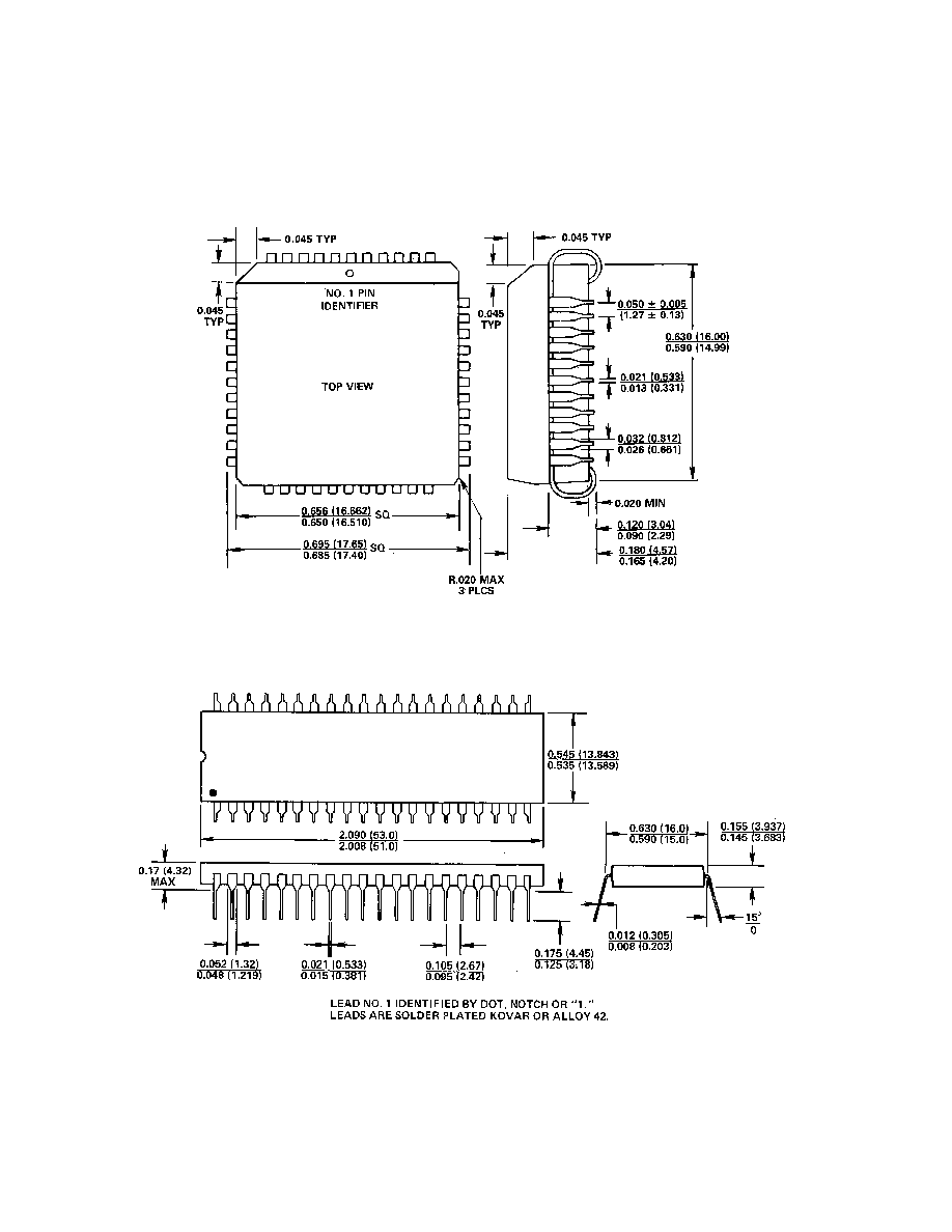
OUTLINE DIMENSIONS
Dimensions shown in inches and (mm).
44-Terminal Plastic Leaded Chip Carrier
(P-44A)
40-Pin Plastic DIP
(N-40A)
C1391244/90
PRINTED IN U.S.A.