 | ÐлекÑÑоннÑй компоненÑ: ADV7150 | СкаÑаÑÑ:  PDF PDF  ZIP ZIP |
Äîêóìåíòàöèÿ è îïèñàíèÿ www.docs.chipfind.ru
REV. A
Information furnished by Analog Devices is believed to be accurate and
reliable. However, no responsibility is assumed by Analog Devices for its
use, nor for any infringements of patents or other rights of third parties
which may result from its use. No license is granted by implication or
otherwise under any patent or patent rights of Analog Devices.
a
CMOS 220 MHz True-Color Graphics
Triple 10-Bit Video RAM-DAC
ADV7150
© Analog Devices, Inc., 1996
One Technology Way, P.O. Box 9106, Norwood, MA 02062-9106, U.S.A.
Tel: 617/329-4700
Fax: 617/326-8703
@
85
MHz
8-Bit Pseudo Color
15-Bit True Color
APPLICATIONS
High Resolution, True Color Graphics
Professional Color Prepress Imaging
GENERAL DESCRIPTION
The ADV7150 (ADV
®
) is a complete analog output, Video
RAM-DAC on a single CMOS monolithic chip. The part is spe-
cifically designed for use in high performance, color graphics
workstations. The ADV7150 integrates a number of graphic
functions onto one device allowing 24-bit direct True-Color op-
eration at the maximum screen update rate of 220 MHz. The
ADV7150 implements 30-bit True Color in 24-bit frame buffer
designs. The part also supports other modes, including 15-bit
True Color and 8-bit Pseudo or Indexed Color. Either the Red,
Green or Blue input pixel ports can be used for Pseudo Color.
(Continued on page 12)
ADV is a registered trademark of Analog Devices, Inc.
FEATURES
220 MHz, 24-Bit (30-Bit Gamma Corrected) True Color
Triple 10-Bit "Gamma Correcting" D/A Converters
Triple 256 10 (256 30) Color Palette RAM
On-Chip Clock Control Circuit
Palette Priority Select Registers
RS-343A/RS-170 Compatible Analog Outputs
TTL Compatible Digital Inputs
Standard MPU l/O Interface
10-Bit Parallel Structure
8+2 Byte Structure
Programmable Pixel Port: 24-Bit, 15-Bit and
Programmable Pixel Port:
8-Bit (Pseudo)
Pixel Data Serializer
Multiplexed Pixel Input Ports; 1:1, 2:1, 4:1
+5 V CMOS Monolithic Construction
160-Lead Plastic Quad Flatpack (QFP)
Thermally Enhanced to Achieve
JC
< 1.0 C/W
MODES OF OPERATION
24-Bit True Color (30-Bit Gamma Corrected)
@ 220 MHz
@ 170 MHz
@ 135 MHz
@ 110 MHz
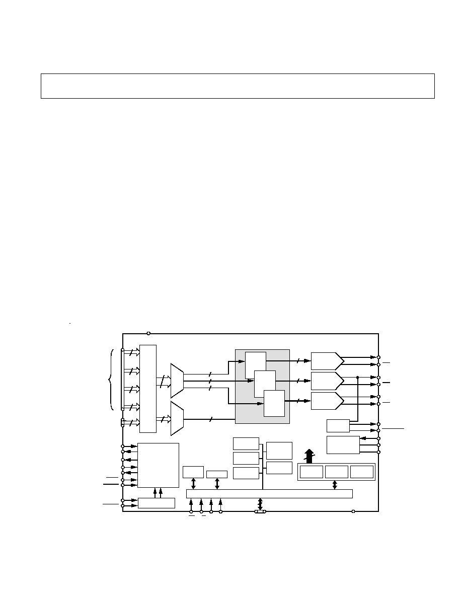
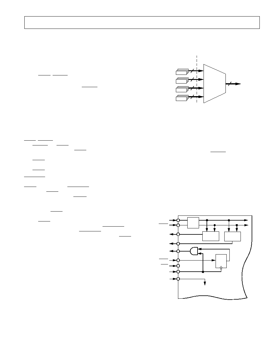
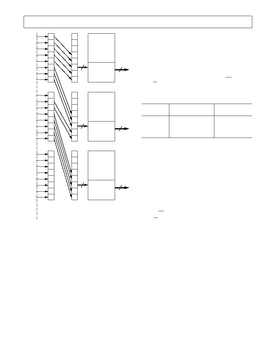
FUNCTIONAL BLOCK DIAGRAM
256-COLOR/GAMMA
PALETTE RAM
10
10-BIT
RED DAC
10-BIT
BLUE DAC
IOR
96
C
D
A
B
24
24
24
24
P
I
X
E
L
P
O
R
T
MUX
4:1
30
RED
256 x 10
MPU PORT
D9 D0
10 (8+2)
CE R/W C0 C1
LOADIN
CLOCK
LOADOUT
PRGCKOUT
SCKIN
SCKOUT
CLOCK DIVIDE
&
SYNCHRONIZATION
CIRCUIT
÷
32
÷
16,
÷
8,
÷
4,
÷
2
ADDR
(A7A0)
REVISION
REGISTER
COMMAND
REGISTERS
(CR1CR3)
TEST
REGISTERS
(MR1)
VOLTAGE
REFERENCE
CIRCUIT
ECL TO CMOS
ADV7150
V
REF
R
SET
C
OMP
SYNC
OUTPUT
I
PLL
RED (R7R0),
GREEN (G7G0),
BLUE (B7B0)
COLOR DATA
V
AA
GND
DATA TO
PALETTES
CONTROL REGISTERS
COLOR REGISTERS
CLOCK CONTROL
MODE
REGISTER
ADDRESS
REGISTER
GREEN
256 x 10
BLUE
256 x 10
PALETTE
SELECTS
(PS0, PS1)
ID
REGISTER
GREEN
REGISTER
PIXEL MASK
REGISTER
8
IOR
IOG
IOG
IOB
IOB
10-BIT
GREEN DAC
10
10
BLUE
REGISTER
RED
REGISTER
8
8
2
8
8
SYNC
BLANK
CLOCK
SYNCOUT
MUX
4:1
REV. A
2
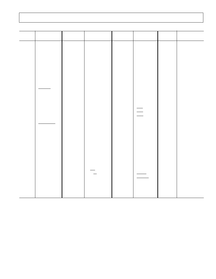
ADV7150SPECIFICATIONS
(V
AA
1
= +5 V; V
REF
= +1.235 V; R
SET
= 280
. IOR, IOG, IOB (R
L
= 37.5
,
C
L
= 10 pF); IOR, IOG, IOB = GND. All specifications T
MIN
to T
MAX
2
unless otherwise noted.)
Parameter
All Versions
Unit
Test Conditions/Comments
STATIC PERFORMANCE
Resolution (Each DAC)
10
Bits
Accuracy (Each DAC)
Integral Nonlinearity
±
1
LSB max
Differential Nonlinearity
±
1
LSB max
Guaranteed Monotonic
Gray Scale Error
±
5
% Gray Scale max
Coding
Binary
DIGITAL INPUTS (Excluding CLOCK, CLOCK)
Input High Voltage, V
INH
2
V min
Input Low Voltage, V
INL
0.8
V max
Input Current, I
IN
±
10
µ
A max
V
IN
= 0.4 V or 2.4 V
Input Capacitance, C
IN
10
pF max
CLOCK INPUTS (CLOCK, CLOCK)
Input High Voltage, V
INH
V
AA
1.0
V min
Input Low Voltage, V
INL
V
AA
1.6
V max
Input Current, I
IN
±
10
µ
A max
V
IN
= 0.4 V or 2.4 V
Input Capacitance, C
IN
10
pF typ
DIGITAL OUTPUT
Output High Voltage, V
OH
2.4
V min
I
SOURCE
= 400
µ
A
Output Low Voltage, V
OL
0.4
V max
I
SINK
= 3.2 mA
Floating-State Leakage Current
20
µ
A max
Floating-State Output Capacitance
20
pF typ
ANALOG OUTPUTS
Gray Scale Current Range
15/22
mA min/max
Output Current
White Level Relative to Blank
17.69/20.40
mA min/max
Typically 19.05 mA
White Level Relative to Black
16.74/18.50
mA min/max
Typically 17.62 mA
Black Level Relative to Blank
0.95/1.90
mA min/max
Typically 1.44 mA
Blank Level on IOR, IOB
0/50
µ
A min/max
Typically 5
µ
A
Blank Level on IOG
6.29/8.96
mA min/max
Typically 7.62 mA
Sync Level on IOG
0/50
µ
A min/max
Typically 5
µ
A
LSB Size
17.22
µ
A typ
DAC-to-DAC Matching
3
% max
Typically 1%
Output Compliance, V
OC
0/+1.4
V min/V max
Output Impedance, R
OUT
100
k
typ
Output Capacitance, C
OUT
30
pF max
I
OUT
= 0 mA
VOLTAGE REFERENCE
Voltage Reference Range, V
REF
1.14/1.26
V min/V max
V
REF
= 1.235 V for Specified Performance
Input Current, I
VREF
+5
µ
A typ
POWER REQUIREMENTS
V
AA
5
V nom
I
AA
3
400
mA max
220 MHz Parts
I
AA
3
370
mA max
170 MHz Parts
I
AA
350
mA max
135 MHz Parts
I
AA
330
mA max
110 MHz Parts
I
AA
315
mA max
85 MHz Parts
Power Supply Rejection Ratio
0.5
%/% max
Typically 0.12%/%: COMP = 0.1
µ
F
DYNAMIC PERFORMANCE
Clock and Data Feedthrough
4, 5
30
dB typ
Glitch Impulse
50
pV secs typ
DAC-to-DAC Crosstalk
6
23
dB typ
NOTES
1
±
5% for all versions.
2
Temperature range (T
MIN
to T
MAX
): 0
°
C to +70
°
C; T
J
(Silicon Junction Temperature)
100
°
C.
3
Pixel Port is continuously clocked with data corresponding to a linear ramp. T
J
= 100
°
C.
4
Clock and data feedthrough is a function of the amount of overshoot and undershoot on the digital inputs. Glitch impulse includes clock and data feedthrough.
5
TTL input values are 0 to 3 volts, with input rise/fall times
3 ns, measured the 10% and 90% points. Timing reference points at 50% for inputs and outputs.
6
DAC-to-DAC crosstalk is measured by holding one DAC high while the other two are making low-to-high and high-to-low transitions.
Specifications subject to change without notice.
ADV7150
3
REV. A
TIMING CHARACTERISTICS
1
CLOCK CONTROL AND PIXEL PORT
4
220 MHz 170 MHz 135 MHz 110 MHz 85 MHz
Parameter
Version
Version
Version
Version
Version
Units
Conditions/Comments
f
CLOCK
220
170
135
110
85
MHz max Pixel CLOCK Rate
t
1
4.55
5.88
7.4
9.1
11.77
ns min
Pixel CLOCK Cycle Time
t
2
2
2.5
3.2
4
4
ns min
Pixel CLOCK High Time
t
3
2
2.5
3
4
4
ns min
Pixel CLOCK Low Time
t
4
10
10
10
10
10
ns max
Pixel CLOCK to LOADOUT Delay
f
LOADIN
LOADIN Clocking Rate
1:1 Multiplexing
110
110
110
110
85
MHz max
2:1 Multiplexing
110
85
67.5
55
42.5
MHz max
4:1 Multiplexing
55
42.5
33.75
27.5
21.25
MHz max
t
5
LOADIN Cycle Time
1:1 Multiplexing
9.1
9.1
9.1
9.1
9.1
ns min
2:1 Multiplexing
9.1
11.76
14.8
18.18
23.53
ns min
4:1 Multiplexing
18.18
23.53
29.63
36.36
47.1
ns min
t
6
LOADIN High Time
1:1 Multiplexing
4
4
4
4
4
ns min
2:1 Multiplexing
4
5
6
8
9
ns min
4:1 Multiplexing
8
9
12
15
18
ns min
t
7
LOADIN Low Time
1:1 Multiplexing
4
4
4
4
4
ns min
2:1 Multiplexing
4
5
6
8
9
ns min
4:1 Multiplexing
8
9
12
15
18
ns min
t
8
0
0
0
0
0
ns min
Pixel Data Setup Time
t
9
5
5
5
5
5
ns min
Pixel Data Hold Time
t
10
0
0
0
0
0
ns min
LOADOUT to LOADIN Delay
t
11
5
5
5
5
5
5
ns max
LOADOUT to LOADIN Delay
t
PD
6
Pipeline Delay
1:1 Multiplexing
5
5
5
5
5
CLOCKs
(1
×
CLOCK = t
1
)
2:1 Multiplexing
6
6
6
6
6
CLOCKs
4:1 Multiplexing
8
8
8
8
8
CLOCKs
t
12
10
10
10
10
10
ns max
Pixel CLOCK to PRGCKOUT Delay
t
13
5
5
5
5
5
ns max
SCKIN to SCKOUT Delay
t
14
5
5
5
5
5
ns min
BLANK
to SCKIN Setup Time
t
15
1
1
1
1
1
ns min
BLANK
to SCKIN Hold Time
ANALOG OUTPUTS
7
220 MHz 170 MHz 135 MHz 110 MHz 85 MHz
Parameter
Version
Version
Version
Version
Version
Units
Conditions/Comments
t
16
15
15
15
15
15
ns typ
Analog Output Delay
t
17
1
1
1
1
1
ns typ
Analog Output Rise/Fall Time
t
18
15
15
15
15
15
ns typ
Analog Output Transition Time
t
SK
2
2
2
2
2
ns max
Analog Output Skew (IOR, IOG, IOB)
0
0
0
0
0
ns typ
MPU PORTS
8, 9
220 MHz 170 MHz 135 MHz 110 MHz 85 MHz
Parameter
Version
Version
Version
Version
Version
Units
Conditions/Comments
t
19
3
3
3
3
3
ns min
R/W, C0, C1 to CE Setup Time
t
20
10
10
10
10
10
ns min
R/W, C0, C1 to CE Hold Time
t
21
45
45
45
45
45
ns min
CE
Low Time
t
22
25
25
25
25
25
ns min
CE
High Time
t
23
8
5
5
5
5
5
ns min
CE
Asserted to Databus Driven
t
24
9
45
45
45
45
45
ns max
CE
Asserted to Data Valid
t
25
9
20
20
20
20
20
ns max
CE
Disabled to Databus Three-Stated
5
5
5
5
5
ns min
t
26
20
20
20
20
20
ns min
Write Data (D0D9) Setup Time
t
27
5
5
5
5
5
ns min
Write Data (D0D9) Hold Time
(V
AA
2
= +5 V; V
REF
= +1.235 V; R
SET
= 280
. IOR, IOG, IOB (R
L
= 37.5
, C
L
= 10 pF);
IOR
, IOG, I0B = GND. All specifications T
MIN
to T
MAX
3
unless otherwise noted.)
ADV7150
4
REV. A
NOTES
1
TTL input values are 0 to 3 volts, with input rise/fall times
3 ns, measured between the 10% and 90% points. ECL inputs (CLOCK, CLOCK) are
V
AA
0.8 V to V
AA
1.8 V, with input rise/fall times
2 ns, measured between the 10% and 90% points. Timing reference points at 50% for inputs and out-
puts. Analog output load
10 pF. Databus (D0D9) loaded as shown in Figure 1. Digital output load for LOADOUT, PRGCKOUT, SCKOUT, I
PLL
and
SYNCOUT
30 pF.
2
±
5% for all versions.
3
Temperature range (T
MIN
to T
MAX
): 0
°
C to +70
°
C; T
J
(Silicon Junction Temperature)
100
°
C.
4
Pixel Port consists of the following inputs: Pixel Inputs: RED [A, B, C, D]; GREEN [A, B, C, D]; BLUE [A, B, C, D], Palette Selects: PS0 [A, B, C, D]; PS1
[A, B, C, D]; Pixel Controls: SYNC, BLANK; Clock Inputs: CLOCK, CLOCK, LOADIN, SCKIN; Clock Outputs: LOADOUT, PRGCKOUT, SCKOUT.
5
is the LOADOUT Cycle Time and is a function of the Pixel CLOCK Rate and the Multiplexing Mode: 1:1 multiplexing;
= CLOCK = t
1
ns. 2:1 Multi-
plexing;
= CLOCK
×
2 = 2
×
t
1
ns. 4:1 Multiplexing;
= CLOCK
×
4 = 4
×
t
1
ns.
6
These fixed values for Pipeline Delay are valid under conditions where t
10
and
-t
11
are met. If either t
10
or
-t
11
are not met, the part will operate but the Pipe line De-
lay is increased by 2 additional CLOCK cycles for 2:1 Mode and is increased by 4 additional CLOCK cycles for 4:1 Mode, after calibration is performed.
7
Output delay measured from the 50% point of the rising edge of CLOCK to the 50% point of full-scale transition. Output rise/fall time measured between the 10%
and 90% points of full-scale transition. Transition time measured from the 50% point of full-scale transition to the output remaining within 2% of the final output
value (Transition time does not include clock and data feedthrough).
8
t
23
and t
24
are measured with the load circuit of Figure 1 and defined as the time required for an output to cross 0.4 V or 2.4 V.
9
t
25
is derived from the measured time taken by the data outputs to change by 0.5 V when loaded with the circuit of Figure 1. The measured number is then extrapo-
lated back to remove the effects of charging the 100 pF capacitor. This means that the time, t
25
, quoted in the Timing Characteristics is the true value for the device
and as such is independent of external databus loading capacitances.
Specifications subject to change without notice.
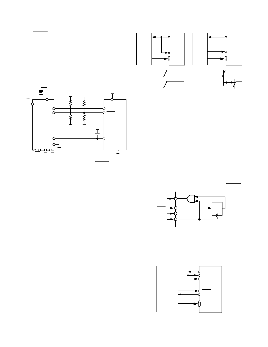
I
SINK
+2.1V
TO
OUTPUT
PIN
I
SOURCE
100pF
Figure 1. Load Circuit for Databus Access and Relinquish Times
t
3
t
2
CLOCK
LOADOUT
(1:1 MULTIPLEXING)
LOADOUT
(2:1 MULTIPLEXING)
LOADOUT
(4:1 MULTIPLEXING)
CLOCK
t
4
t
1
Figure 2. LOADOUT vs. Pixel Clock Input (CLOCK, CLOCK)
PIXEL INPUT
DATA*
LOADIN
t
8
t
9
VALID
DATA
VALID
DATA
VALID
DATA
t
5
t
6
*INCLUDES PIXEL DATA (R0R7, G0G7, B0B7); PALETTE SELECT INPUTS (PS0PS1); BLANK; SYNC
t
7
Figure 3. LOADIN vs. Pixel Input Data
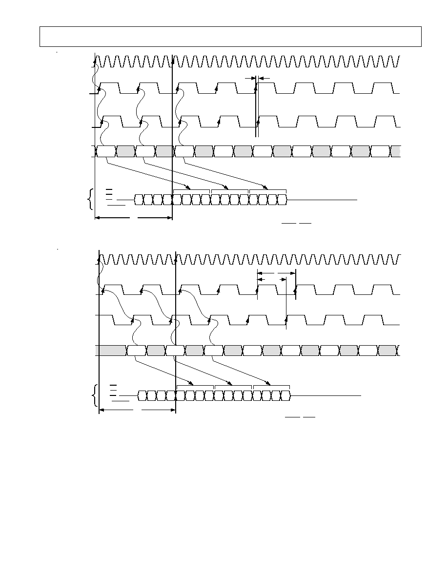
ADV7150
5
REV. A
PIXEL INPUT
DATA*
A
N+2
B
N+2
C
N+2
D
N+2
CLOCK
LOADOUT
LOADIN
ANALOG
OUTPUT
DATA
t
10
t
PD
DIGITAL INPUT TO ANALOG
OUTPUT PIPELINE
A
N
B
N
C
N
D
N
*INCLUDES PIXEL DATA (R0R7, G0G7, B0B7); PALETTE SELECT INPUTS (PS0PS1); BLANK; SYNC
A
N+1
B
N+1
C
N+1
D
N+1
A
N
B
N
C
N
D
N
A
N+1
B
N+1
C
N+1
D
N+1
A
N1
B
N1
C
N1
D
N1
A
N+2
B
N+2
C
N+2
D
N+2
IOR, IOR
IOG, IOG
IOB, IOB
IPLL, SYNCOUT
Figure 4. Pixel Input to Analog Output Pipeline with Minimum LOADOUT to LOADIN Delay (4:1 Multiplex Mode)
DIGITAL INPUT
TO ANALOG
OUTPUT
PIPELINE
A
N+2
B
N+2
C
N+2
D
N+2
CLOCK
LOADOUT
PIXEL INPUT
DATA*
LOADIN
ANALOG
OUTPUT
DATA
A
N
B
N
C
N
D
N
A
N
B
N
C
N
D
N
A
N+1
B
N+1
C
N+1
D
N+1
A
N1
B
N1
C
N1
D
N1
A
N+2
B
N+2
C
N+2
D
N+2
t
PD
t
11
*INCLUDES PIXEL DATA (R0R7, G0G7, B0B7); PALETTE SELECT INPUTS (PS0PS1); BLANK; SYNC
IOR, IOR
IOG, IOG
IOB, IOB
IPLL, SYNCOUT
A
N+1
B
N+1
C
N+1
D
N+1
Figure 5. Pixel Input to Analog Output Pipeline with Maximum LOADOUT to LOADIN Delay (4:1 Multiplex Mode)
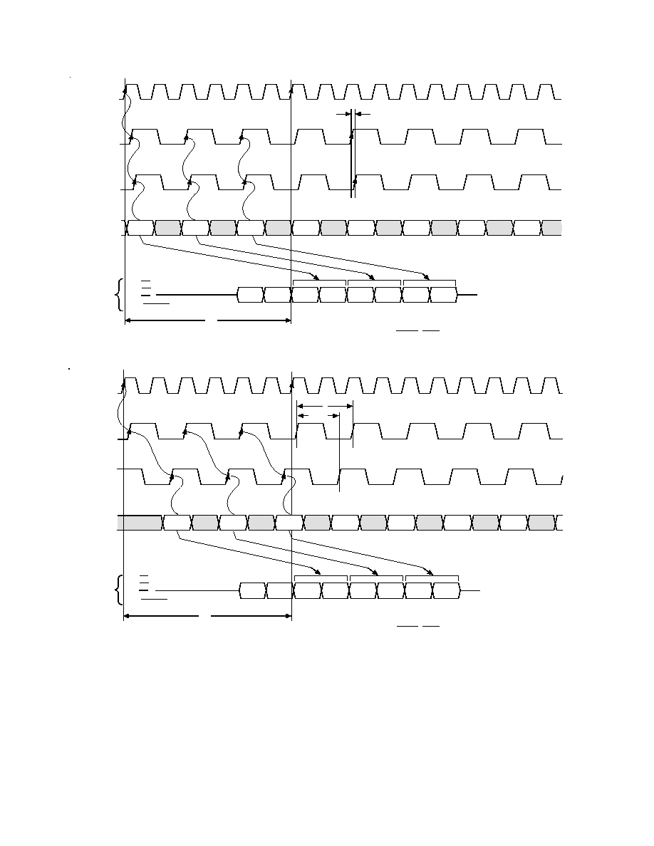
ADV7150
6
REV. A
PIXEL INPUT
DATA*
A
N
B
N
t
PD
A
N
B
N
A
N-1
B
N-1
A
N+1
B
N+1
A
N+2
B
N+2
*INCLUDES PIXEL DATA (R0R7, G0G7, B0B7); PALETTE SELECT INPUTS (PS0PS1); BLANK; SYNC
CLOCK
LOADOUT
LOADIN
ANALOG
OUTPUT
DATA
t
10
DIGITAL INPUT TO ANALOG
OUTPUT PIPELINE
A
N+1
B
N+1
A
N+2
B
N+2
IOR, IOR
IOG, IOG
IOB, IOB
IPLL, SYNCOUT
Figure 6. Pixel Input to Analog Output Pipeline with Minimum LOADOUT to LOADIN Delay (2:1 Multiplex Mode)
CLOCK
LOADOUT
PIXEL INPUT
DATA*
LOADIN
ANALOG
OUTPUT
DATA
t
PD
DIGITAL INPUT TO ANALOG
OUTPUT PIPELINE
A
N
B
N
A
N+1
B
N+1
A
N
B
N
A
N-1
B
N-1
A
N+1
B
N+1
A
N+2
B
N+2
*INCLUDES PIXEL DATA (R0R7, G0G7, B0B7); PALETTE SELECT INPUTS (PS0PS1); BLANK; SYNC
t
11
A
N+2
B
N+2
IOR, IOR
IOG, IOG
IOB, IOB
IPLL, SYNCOUT
Figure 7. Pixel Input to Analog Output Pipeline with Maximum LOADOUT to LOADIN Delay (2:1 Multiplex Mode)
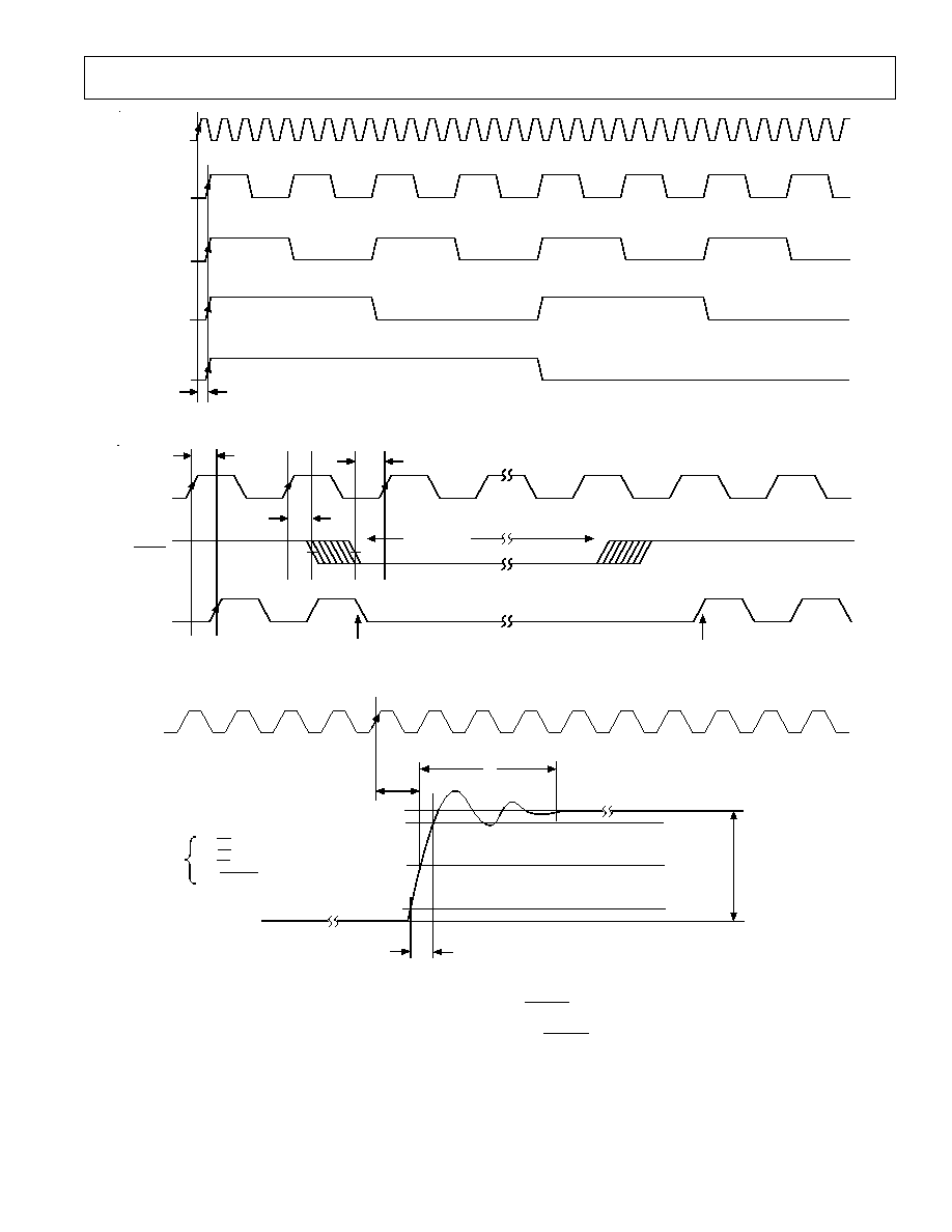
ADV7150
7
REV. A
t
12
CLOCK
PRGCKOUT
(CLOCK/4)
PRGCKOUT
(CLOCK/8)
PRGCKOUT
(CLOCK/16)
PRGCKOUT
(CLOCK/32)
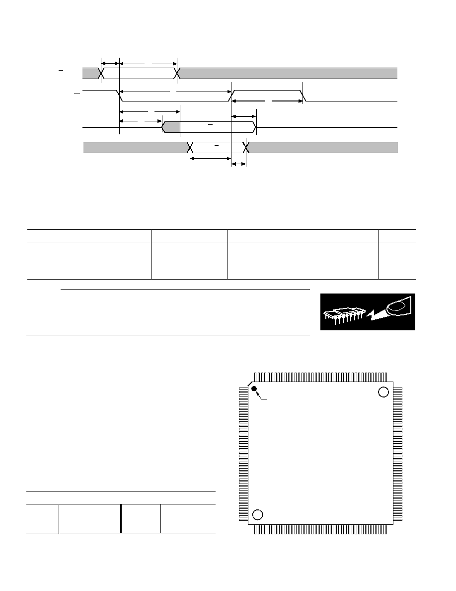
Figure 8. Pixel Clock Input vs. Programmable Clock Output (PRGCKOUT)
SCKIN
END OF SCAN LINE (N)
t
13
SCKOUT
START OF SCAN LINE (N+1)
BLANKING
PERIOD
t
15
t
14
BLANK
Figure 9. Video Data Shift Clock Input (SCKIN) & BLANK vs. Video Data Shift Clock Output (SCKOUT)
CLOCK
t
16
ANALOG
OUTPUTS
t
17
t
18
10 %
50 %
90 %
FULL-SCALE
TRANSITION
WHITE LEVEL
BLACK LEVEL
IOR, IOR
IOG, IOG
IOB, IOB
IPLL, SYNCOUT
NOTE:
THIS DIAGRAM IS NOT TO SCALE. FOR THE PURPOSES OF
CLARITY, THE ANALOG OUTPUT WAVEFORM IS MAGNIFIED IN
TIME AND AMPLITUDE W.R.T THE CLOCK WAVEFORM.
IPLL AND SYNCOUT ARE DIGITAL VIDEO OUTPUT SIGNALS.
t
16
IS THE ONLY RELEVENT OUTPUT TIMING SPECIFICATION
FOR I
PLL
AND SYNCOUT.
Figure 10. Analog Output Response vs. CLOCK
ADV7150
8
REV. A
RECOMMENDED OPERATING CONDITION
Parameter
Symbol
Min
Typ
Max
Units
Power Supply
V
AA
4.75
5.00
5.25
Volts
Ambient Operating Temperature
T
A
0
+70
°
C
Reference Voltage
V
REF
1.14
1.235
1.26
Volts
Output Load
R
L
37.5
WARNING!
ESD SENSITIVE DEVICE
CAUTION
ESD (electrostatic discharge) sensitive device. Electrostatic charges as high as 4000 V readily
accumulate on the human body and test equipment and can discharge without detection.
Although the ADV7150 features proprietary ESD protection circuitry, permanent damage may
occur on devices subjected to high energy electrostatic discharges. Therefore, proper ESD
precautions are recommended to avoid performance degradation or loss of functionality.
ABSOLUTE MAXIMUM RATINGS
1
V
AA
to GND . . . . . . . . . . . . . . . . . . . . . . . . . . . . . . . . . . . 7 V
Voltage on Any Digital Pin . . . . GND 0.5 V to V
AA
+ 0.5 V
Ambient Operating Temperature (T
A
) . . . . . 55
°
C to +125
°
C
Storage Temperature (T
S
) . . . . . . . . . . . . . . 65
°
C to +150
°
C
Junction Temperature (T
J
) . . . . . . . . . . . . . . . . . . . . +150
°
C
Lead Temperature (Soldering, 10 secs) . . . . . . . . . . . +260
°
C
Vapor Phase Soldering (1 minute) . . . . . . . . . . . . . . . +220
°
C
Analog Outputs to GND
2
. . . . . . . . . . . . . GND 0.5 to V
AA
NOTES
1
Stresses above those listed under "Absolute Maximum Ratings" may cause
permanent damage to the device. This is a stress rating only and functional
operation of the device at these or any other conditions above those listed in the
operational sections of this specification is not implied. Exposure to absolute
maximum rating conditions for extended periods may affect device reliability.
2
Analog Output Short Circuit to any Power Supply or Common can be of an
indefinite duration.
ORDERING GUIDE
1, 2, 3
Speed
220 MHz
ADV7150LS220
110 MHz
ADV7150LS110
170 MHz
ADV7150LS170
85 MHz
ADV7150LS85
135 MHz
ADV7150LS135
NOTES
1
ADV7150 is packaged in a 160-pin plastic quad flatpack, QFP.
2
All devices are specified for 0
°
C to +70
°
C operation.
3
Contact sales office for latest information on package design.
16-Lead QFP Configuration
ROW D
PIN NO. 1
IDENTIFIER
ROW A
ROW C
ADV7150 QFP
TOP VIEW
(NOT TO SCALE)
ROW B
160
121
41
80
1
40
120
81
t
19
t
20
VALID
CONTROL DATA
t
21
t
22
t
23
t
26
t
25
t
27
D0D9
(READ MODE)
D0D9
(WRITE MODE)
CE
R/W, C0, C1
R/W = 1
R/W = 0
t
24
Figure 11. Microprocessor Port (MPU) Interface Timing
ADV7150
9
REV. A
ADV7150 PIN ASSIGNMENTS
Pin
Pin
Pin
Pin
Number
Mnemonic
Number
Mnemonic
Number
Mnemonic
Number
Mnemonic
1
G3
A
41
PS1
D
81
NC
121
R1
A
2
G3
B
42
B0
A
82
D2
122
R1
B
3
G3
C
43
B0
B
83
NC
123
R1
C
4
G3
D
44
B0
C
84
GND
124
R1
D
5
G4
A
45
B0
D
85
GND
125
R2
A
6
G4
B
46
B1
A
86
GND
126
R2
B
7
G4
C
47
B1
B
87
D3
127
R2
C
8
G4
D
48
B1
C
88
D4
128
R2
D
9
G5
A
49
B1
D
89
D5
129
R3
A
10
G5
B
50
B2
A
90
V
AA
130
R3
B
11
G5
C
5 1
B2
B
91
D6
131
R3
C
12
G5
D
52
B2
C
92
D7
132
R3
D
13
CLOCK
53
B2
D
93
D8
133
R4
A
14
CLOCK
54
B3
A
94
D9
134
R4
B
15
LOADIN
55
B3
B
95
GND
135
R4
C
16
LOADOUT
56
B3
C
96
GND
136
R4
D
17
V
AA
57
B3
D
97
GND
137
R5
A
18
V
AA
58
B4
A
98
IOB
138
R5
B
19
PRGCKOUT
59
B4
B
99
IOR
139
R5
C
20
SCKIN
60
B4
C
100
IOG
140
R5
D
21
SCKOUT
61
B4
D
101
IOB
141
R6
A
22
SYNCOUT
62
B5
A
102
IOG
142
R6
B
23
GND
63
B5
B
103
V
AA
143
R6
C
24
GND
64
B5
C
104
V
AA
144
R6
D
25
GND
65
B5
D
105
V
AA
145
R7
A
26
G6
A
66
B6
A
106
IOR
146
R7
B
27
G6
B
67
B6
B
107
COMP
147
R7
C
28
G6
C
68
B6
C
108
V
REF
148
R7
D
29
G6
D
69
B6
D
109
R
SET
149
G0
A
30
G7
A
70
B7
A
110
I
PLL
150
G0
B
31
G7
B
71
B7
B
111
GND
151
G0
C
32
G7
C
72
B7
C
112
V
AA
152
G0
D
33
G7
D
73
B7
D
113
V
AA
153
G1
A
34
PS0
A
74
CE
114
V
AA
154
G1
B
35
PS0
B
75
R/W
115
SYNC
155
G1
C
36
PS0
C
76
C0
116
BLANK
1 56
G1
D
37
PS0
D
77
C1
117
R0
A
157
G2
A
38
PS1
A
78
D0
118
R0
B
158
G2
B
39
PS1
B
79
D1
119
R0
C
159
G2
C
40
PS1
C
80
GND
120
R0
D
160
G2
D
NC = No Connect.
ADV7150
10
REV. A
PIN FUNCTION DESCRIPTION
Mnemonic
Function
RED (R0
A
. . . R0
D
R7
A
. . . R7
D
),
Pixel Port (TTL Compatible Inputs): 96 pixel select inputs, with 8 bits each for Red, 8
GREEN (G0
A
. . . G0
D
G7
A
. . . G7
D
),
bits for Green and 8 bits for Blue. Each bit is multiplexed [A-D] 4:1, 2:1 or 1:1. It can
BLUE (B0
A
. . . B0
D
B7
A
. . . B7
D
)
be configured for 24-Bit True-Color Data, 8-Bit Pseudo-Color Data and 15-Bit True-Color
Data formats. Pixel Data is latched into the device on the rising edge of LOADIN.
PS0
A
. . . PS0
D
, PS1
A
. . . PS1
D
Palette Priority Selects (TTL Compatible Inputs): These pixel port select inputs deter-
mine whether or not the device's pixel data port is selected on a pixel by pixel basis.
The palette selects allow switching between multiple palette devices. The device can be
preprogrammed to completely shut off the DAC analog outputs. If the values of PS0
and PS1 match the values programmed into bits MR16 and MR17 of the Mode Regis-
ter, then the device is selected. Each bit is multiplexed [A-D] 4:1, 2:1 or 1:1. PS0 and
PS1 are latched into the device on the rising edge of LOADIN.
LOADIN
Pixel Data Load Input (TTL Compatible Input). This input latches the multiplexed
pixel data, including PS0PS1, BLANK and SYNC into the device.
LOADOUT
Pixel Data Load Output (TTL Compatible Output). This output control signal runs at
a divided down frequency of the pixel CLOCK input. Its frequency is a function of the
multiplex rate. It can be used to directly or indirectly drive LOADIN
f
LOADOUT
= f
CLOCK
/M
where M = 1 for 1:1 Multiplex Mode
where
M = 2 for 2:1 Multiplex Mode
where
M = 4 for 4:1 Multiplex Mode.
PRGCKOUT
Programmable Clock Output (TTL Compatible Output). This output control signal
runs at a divided down frequency of the pixel CLOCK input. Its frequency is user
programmable and is determined by bits CR30 and CR31 of Command Register 3
f
PRGCKOUT
= f
CLOCK
/N
where N = 4, 8, 16 and 32.
SCKIN
Video Shift Clock Input (TTL Compatible Input). The signal on this input is internally
gated synchronously with the BLANK signal. The resultant output, SCKOUT, is a
video clocking signal that is stopped during video blanking periods.
SCKOUT
Video Shift Clock Output (TTL Compatible Output). This output is a synchronously
gated version of SCKIN and BLANK. SCKOUT, is a video clocking signal that is
stopped during video blanking periods.
CLOCK, CLOCK
Clock Inputs (ECL Compatible Inputs). These differential clock inputs are designed to
be driven by ECL logic levels configured for single supply (+5 V) operation. The clock
rate is normally the pixel clock rate of the system.
BLANK
Composite Blank (TTL Compatible Input). This video control signal drives the analog
outputs to the blanking level.
SYNC
Composite-Sync Input (TTL Compatible Input). This video control signal drives the
IOG analog output to the SYNC level. It is only asserted during the blanking period.
CR22 in Command Register 2 must be set if SYNC is to be decoded onto the analog
output, otherwise the SYNC input is ignored.
SYNCOUT
Composite-Sync Output (TTL Compatible Output). This video output is a delayed
version of SYNC. The delay corresponds to the number of pipeline stages of the device.
D0D9
Databus (TTL Compatible Input/Output Bus). Data, including color palette values and
device control information is written to and read from the device over this 10-bit, bidi-
rectional databus. 10-bit data or 8-bit data can be used. The databus can be configured
for either 10-bit parallel data or byte data (8+2) as well as standard 8-bit data. Any un-
used bits of the databus should be terminated through a resistor to either the digital
power plane (V
CC
) or GND.
CE
Chip Enable (TTL Compatible Input). This input must be at Logic "0," when writing
to or reading from the device over the databus (D0D9). Internally, data is latched on
the rising edge of CE.
ADV7150
11
REV. A
Mnemonic
Function
R/W
Read/Write Control (TTL Compatible Input). This input determines whether data is
written to or read from the device's registers and color palette RAM. R/W and CE must
be at Logic "0" to write data to the part. R/W must be at Logic "1" and CE at Logic
"0" to read from the device.
C0, C1
Command Controls (TTL Compatible Inputs). These inputs determine the type of read
or write operation being performed on the device over the databus (see Interface Truth
Table). Data on these inputs is latched on the falling edge of CE.
IOR; IOR, IOG; IOG, IOB;
Red, Green and Blue Current Outputs (High Impedance Current Sources). These RGB
IOB
video outputs are specified to directly drive RS-343A and RS-170 video levels into dou-
bly terminated 75
loads.
IOR
, IOG and IOB are the complementary outputs of IOR, IOG and IOB. These out-
puts can be tied to GND if it is not required to use differential outputs.
V
REF
Voltage Reference Input (Analog Input). An external 1.235 V voltage reference is re-
quired to drive this input. An AD589 (2-terminal voltage reference) or equivalent is rec-
ommended. (Note: It is not recommended to use a resistor network to generate the
voltage reference.)
R
SET
Output Full-Scale Adjust Control (Analog Input). A resistor connected between this pin
and analog ground controls the absolute amplitude of the output video signal. The value
of R
SET
is derived from the full-scale output current on IOG according to the following
equations:
R
SET
(
) = C1
×
V
REF
/IOG (mA); SYNC on GREEN
R
SET
(
) = C2
×
V
REF
/IOG (mA); NO SYNC on GREEN.
Full-Scale output currents on IOR and IOB for a particular value of R
SET
are given by:
IOR (mA)= C2
×
V
REF
(V)/R
SET
(
)
and
IOB (mA) = C2
×
V
REF
(V)/R
SET
(
)
where
C1 = 6,050; PEDESTAL = 7.5 IRE
where
C1
= 5,723; PEDESTAL = 0 IRE
and
where
C2 = 4,323; PEDESTAL = 7.5 IRE
where
C1
= 3,996; PEDESTAL = 0 IRE.
COMP
Compensation Pin. A 0.1
µ
F capacitor should be connected between this pin and V
AA
.
I
PLL
Phase Lock Loop Output Current (High Impedance Current Source). This output is
used to enable multiple ADV7150s along with ADV7151s to be synchronized together
with pixel resolution when using an external PLL. This output is triggered either from
the falling edge of SYNC or BLANK as determined by bit CR21 of Command Register
2. When activated, it supplies a current corresponding to:
I
PLL
(mA) = 1,728
×
V
REF
(V)/R
SET
(
)
When not using the I
PLL
function, this output pin should be tied to GND.
V
AA
Power Supply (+5 V
±
5%). The part contains multiple power supply pins, all should be
connected together to one common +5 V filtered analog power supply.
GND
Analog Ground. The part contains multiple ground pins, all should be connected
together to the system's ground plane.
ADV7150
12
REV. A
CIRCUIT DETAILS AND OPERATION
OVERVIEW
Digital video or pixel data is latched into the ADV7150 over the
devices Pixel Port. This data acts as a pointer to the onboard
Color Palette RAM. The data at the RAM address pointed to is
latched into the digital-to-analog converters (DACs) and output
as an RGB analog video signal.
For the purposes of clarity of description, the ADV7150 is bro-
ken down into three separate functional blocks. These are:
1. Pixel port and clock control circuit
2. MPU port, registers and color palette
3. Digital-to-analog converters and video outputs
Table I shows the architectural and packaging differences be-
tween other devices in the ADV715x series of workstation parts.
(For more details consult the relevant data sheets.)
Table I. Architectural and Packaging Differences of the
ADV715x Series
Description
ADV7150
ADV7152*
ADV7151*
24-Bit "Gamma" True Color
·
·
24-Bit "Standard" True Color
·
·
8-Bit "Gamma" Pseudo Color
·
·
·
8-Bit "Standard" Pseudo Color
·
·
·
15-Bit True Color
·
·
220 MHz True Color
·
·
220 MHz Pseudo Color
·
·
·
Triple 10-Bit DACs
·
·
·
4:1 Multiplexing
·
·
2:1 Multiplexing
·
·
·
1:1 Multiplexing
·
·
·
160-Lead QFP
·
100-Lead QFP
·
·
*See ADV7151 and ADV7150 data sheets for more information on these parts.
(Continued from page 1)
The device consists of three, high speed, 10-bit, video D/A con-
verters (RGB), three 256
×
10 (one 256
×
30) color look-up
tables, palette priority selects, a pixel input data multiplexer/
serializer and a clock generator/divider circuit. The ADV7150 is
capable of 1:1, 2:1 and 4:1 multiplexing. The onboard palette
priority select inputs enable multiple palette devices to be con-
nected together for use in multipalette and window applications.
The part is controlled and programmed through the micropro-
cessor (MPU) port. The part also contains a number of onboard
test registers, associated with self diagnostic testing of the de-
vice. The individual Red, Green and Blue pixel input ports al-
low True-Color, image rendition. True-Color image rendition,
at speeds of up to 220 MHz, is achieved through the use of the
onboard data multiplexer/serializer. The pixel input port's flex-
ibility allows for direct interface to most standard frame buffer
memory configurations.
The 30 bits of resolution, associated with the color look-up table
and triple 10-bit DAC, realizes 24-bit True-Color resolution,
while also allowing for the onboard implementation of lineariza-
tion algorithms, such as Gamma-Correction. This allows effec-
tive 30-Bit True-Color operation.
The on-chip video clock controller circuit generates all the inter-
nal clocking and some additional external clocking signals. An
external ECL oscillator source with differential outputs is all
that is required to drive the CLOCK and CLOCK inputs of the
ADV7150. The part can also be driven by an external clock gen-
erator chip circuit, such as the AD730.
The ADV7150 is capable of generating RGB video output sig-
nals which are compatible with RS-343A and RS-170 video
standards, without requiring external buffering.
Test diagnostic circuitry has been included to complement the
users system level debugging.
The ADV7150 is fabricated in a +5 V CMOS process. Its
monolithic CMOS construction ensures greater functionality
with low power dissipation.
The ADV7150 is packaged in a plastic 160-pin power quad flat-
pack (QFP). Superior thermal dissipation is achieved by inclu-
sion of a copper heatslug, within the standard package outline to
which the die is attached.
Pixel Port and Clock Control Circuit
The Pixel Port of the ADV7150 is directly interfaced to the
video/graphics pipeline of a computer graphics subsystem. It is
connected directly or through a gate array to the video RAM of
the systems Frame-Buffer (video memory). The pixel port on
the device consists of:
Color Data
RED, GREEN, BLUE
Pixel Controls
SYNC
, BLANK
Palette Selects
PS0PS1
The associated clocking signals for the pixel port include:
Clock Inputs
CLOCK, CLOCK,
LOADIN, SCKIN
Clock Outputs
LOADOUT, PRGCKOUT,
SCKOUT
These onboard clock control signals are included to simplify in-
terfacing between the part and the frame buffer. Only two con-
trol input signals are necessary to get the part operational,
CLOCK and CLOCK (ECL Levels). No additional signals or
external glue logic are required to get the Pixel Port & Clock
Control Circuit of the part operational.
Pixel Port (Color Data)
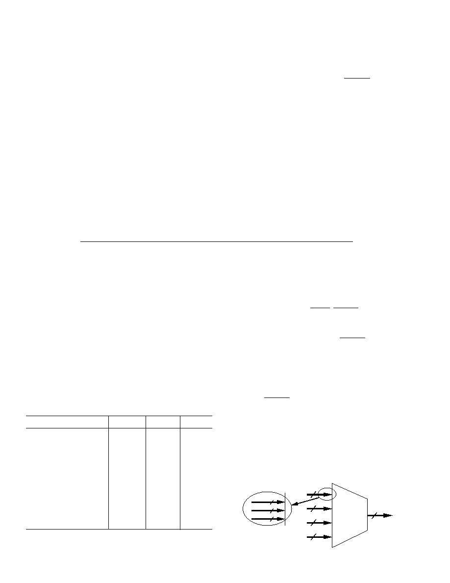
The ADV7150 has 96 color data inputs. The part has four (for
4:1 multiplexing) 24-bit wide direct color data inputs. These are
user programmed to support a number of color data formats in-
cluding 24-Bit True Color, 15-Bit True Color and 8-Bit Pseudo
Color (see "Color Data Formats" section) in 4:1, 2:1 and 1:1
multiplex modes.
A
B
C
D
MULTIPLEXER
24
24
24
24
24
RED
GREEN
BLUE
8
8
8
Figure 12. Multiplexed Color Inputs for the ADV7150
ADV7150
13
REV. A
Multiplexing
The onboard multiplexers of the ADV7150 eliminate the need
for external data serializer circuits. Multiple video memory
devices can be connected, in parallel, directly to the device.
VRAM (BANK A)
VRAM (BANK B)
VRAM (BANK C)
VRAM (BANK D)
MULTIPLEXER
24
24
24
24
24
33MHz
33MHz
33MHz
33MHz
ADV7150
VIDEO MEMORY/ FRAME BUFFER
132 MHz
(4 x 33 MHz)
Figure 13. Direct Interfacing of Video Memory to ADV7150
Figure 13 shows four memory banks of 33 MHz memory con-
nected to the ADV7150, running in 4:1 multiplex mode, giving
a resultant pixel or dot clock rate of 132 MHz. As mentioned in
the previous section, the ADV7150 supports a number of color
data formats in 4:1, 2:1 and 1:1 multiplex modes.
In 1:1 multiplex mode, the ADV7150 is clocked using the
LOADIN signal. This means that there is no requirement for dif-
ferential ECL inputs on CLOCK and CLOCK. The pixel clock is
connected directly to LOADIN. (Note: The ECL CLOCK can
still be used to generate LOADOUT PRGCKOUT, etc.)
CLOCK CONTROL CIRCUIT
The ADV7150 has an integrated Clock Control Circuit (Figure
14). This circuit is capable of both generating the ADV7150's
internal clocking signals as well as external graphics subsystem
clocking signals. Total system synchronization can be attained
by using the parts output clocking signals to drive the control-
ling graphics processor's master clock as well as the video frame
buffers shift clock signals.
CLOCK
ADV7150
CLOCK
DIVIDE BY
N (
÷
N)
LOADOUT
DIVIDE BY
M (
÷
M)
PRGCKOUT
LOADIN
SCKOUT
SCKIN
BLANK
LATCH
ENABLE
SYNC
TO COLOR DATA
MULTIPLEXER
ECL
TO
TTL
M IS A FUNCTION OF MULTIPLEX RATE
M = 4 IN 4:1 MULTIPLEX MODE
M = 2 IN 2:1 MULTIPLEX MODE
M = 1 IN 1:1 MULTIPLEX MODE
N IS INDEPENDENTLY
PROGRAMMABLE
N= (4, 8, 16, 32)
Figure 14. Clock Control Circuit of the ADV7150
Color data is latched into the parts pixel port on every rising
edge of LOADIN (see Timing Waveform, Figure 3). The
required frequency of LOADIN is determined by the multiplex
rate, where:
f
LOADIN
= f
CLOCK
/4
4:1 Multiplex Mode
f
LOADIN
= f
CLOCK
/2
2:1 Multiplex Mode
f
LOADIN
= f
CLOCK
1:1 Multiplex Mode
Other pixel data signals latched into the device by LOADIN
include SYNC, BLANK and PS0PS1.
Internally, data is pipelined through the part by the differential
pixel clock inputs, CLOCK and CLOCK. The LOADIN con-
trol signal needs only have a frequency synchronous relationship
to the pixel CLOCK (see "Pipeline Delay & Onboard Calibra-
tion" section). A completely phase independent LOADIN signal
can be used with the ADV7150, allowing the CLOCK to occur
anywhere during the LOADIN cycle.
Alternatively, the LOADOUT signal of the ADV7150 can be
used. LOADOUT can be connected either directly or indirectly
to LOADIN. Its frequency is automatically set to the correct
LOADIN requirement.
SYNC
, BLANK
The BLANK and SYNC video control signals drive the analog
outputs to the blanking and SYNC levels respectively. These
signals are latched into the part on the rising edge of LOADIN.
The SYNC information is encoded onto the IOG analog signal
when Bit CR22 of Command Register 2 is set to a Logic "1."
The SYNC input is ignored if CR22 is set to "0."
SYNCOUT
In some applications where it is not permissible to encode
SYNC
on green (IOG), SYNCOUT can be used as a separate
TTL digital SYNC output. This has the advantage over an inde-
pendent (of the ADV7150) SYNC in that it does not necessitate
knowing the absolute pipeline delay of the part. This allows
complete independence between LOADIN/Pixel Data and
CLOCK. The SYNC input is connected to the device as normal
with Bit CR22 of Command Register 2 set to "0" thereby pre-
venting SYNC from being encoded onto IOG. Bit CR12 of
Command Register 1 is set to "1," enabling SYNCOUT. The
output signal generates a TTL SYNCOUT with correct pipeline
delay that is capable of directly driving the composite SYNC
signal of a computer monitor.
PS0PS1 (Palette Priority Select Inputs)
These pixel port select inputs determine whether or not the de-
vice is selected. These controls effectively determine whether the
devices RGB analog outputs are turned-on or shut down. When
the analog outputs are shut down, IOR, IOG and IOB are
forced to 0 mA regardless of the state of the pixel and control
data inputs. This state is determined on a pixel by pixel basis as
the PS0PS1 inputs are multiplexed in exactly the same format
as the pixel port color data. These controls allow for switching
between multiple palette devices (see Appendix 4). If the values
of PS0 and PS1 match the values programmed into bits MR16
and MR17 of the Mode Register, then the device is selected, if
there is no match the device is effectively shut down.
ADV7150
14
REV. A
CLOCK, CLOCK Inputs
The Clock Control Circuit is driven by the pixel clock inputs,
CLOCK and CLOCK. These inputs can be driven by a differ-
ential ECL oscillator running from a +5 V supply.
Alternatively, the ADV7150 CLOCK inputs can be driven by a
Programmable Clock Generator (Figure 15), such as the
ICS1562. The ICS1562 is a monolithic, phase-locked-loop,
clock generator chip. It is capable of synthesizing differential
ECL output frequencies in a range up to 220 MHz from a single
low frequency reference crystal.
V
CC
GND
220
330
GND
+5V
CLOCK
CLOCK
CLOCK
GENERATOR
+5V
GND
V
AA
V
CLOCK
ADV7150
GND
D0-D3 CS R/W
ECL
OUT+
V
REF
OUT V
REF
V
AA
0.1
µ
F
LOW FREQUENCY
OSCILLATOR
V
CC
GND
220
330
ECL
OUT
Figure 15. PLL Generator Driving CLOCK, CLOCK of the
ADV7150
CLOCK CONTROL SIGNALS
LOADOUT
The ADV7150 generates a LOADOUT control signal which
runs at a divided down frequency of the pixel CLOCK. The
frequency is automatically set to the programmed multiplex
rate, controlled by CR37 and CR36 of Command Register 3.
f
LOADOUT
= f
CLOCK
/4
4:1 Multiplex Mode
f
LOADOUT
= f
CLOCK
/2
2:1 Multiplex Mode
f
LOADOUT
= f
CLOCK
1:1 Multiplex Mode
The LOADOUT signal is used to directly drive the LOADIN
pixel latch signal of the ADV7150. This is most simply achieved
by tying the LOADOUT and LOADIN pins together. Alterna-
tively, the LOADOUT signal can be used to drive the frame
buffer's shift clock signals, returning to the LOADIN input de-
layed with respect to LOADOUT.
If it is not necessary to have a known fixed number of pipeline
delays, then there is no limitation on the delay between LOAD-
OUT and LOADIN (LOADOUT(1) and LOADOUT(2)).
LOADIN and Pixel Data must conform to the setup and hold
times (t
8
and t
9
).
If, however, it is required that the ADV7150 has a fixed number
of pipeline delays (t
PD
), LOADOUT and LOADIN must con-
form to timing specifications t
10
and
-t
11
as illustrated in Fig-
ures 4 to 7.
LOADOUT
LOADIN
ADV7150
VIDEO
FRAME
BUFFER
LOADOUT
LOADIN
ADV7150
VIDEO
FRAME
BUFFER
LOADOUT(1)
LOADOUT(2)
PIXEL
DATA
PIXEL
DATA
LOADIN
LOADOUT
LOADOUT(1)
LOADOUT(2)
DELAY
Figure 16. LOADOUT vs. Pixel Clock Input (CLOCK, CLOCK)
PRGCKOUT
The PRGCKOUT control signal outputs a user programmable
clock frequency. It is a divided down frequency of the pixel
CLOCK
(see Figure 8). The rising edge of PRGCKOUT is
synchronous to the rising edge of LOADOUT
f
PRGCKOUT
= f
CLOCK
/N
where N = 4, 8, 16 or 32.
One application of the PRGCKOUT is to use it as the master
clock frequency of the graphics subsystems processor or
controller.
SCKIN, SCKOUT
These video memory signals are used to minimize external sup-
port chips. Figure 17 illustrates the function that is provided.
An input signal applied to SCKIN is synchronously AND-ed
with the video blanking signal (BLANK). The resulting signal is
output on SCKOUT. Figure 9 of the Timing Waveform section
shows the relationship between SCKOUT, SCKIN and BLANK.
SCKOUT
SCKIN
BLANK
LATCH
ENABLE
SYNC
Figure 17. SCKOUT Generation Circuit
The SCKOUT signal is essentially the video memory shift con-
trol signal. It is stopped during the screen retrace. Figure 18
shows a suggested frame buffer to ADV7150 interface. This is a
minimum chip solution and allows the ADV7150 control the
overall graphics system clocking and synchronization.
LOADOUT
SCKOUT
ADV7150
VIDEO
FRAME
BUFFER
PIXEL
DATA
LOADIN
SCKIN
BLANK
Figure 18. ADV7150 Interface Using SCKIN and SCKOUT
ADV7150
15
REV. A
Pipeline Delay and Onboard Calibration
The ADV7150 has a fixed number of pipeline delays (t
PD
), so
long as timings t
10
and
-t
11
are met. However, if a fixed pipeline
delay is not a requirement, timings t
10
and
-t
11
can be ignored,
a calibration cycle must be run and there is no restriction on
LOADIN to LOADOUT timing. If timings t
10
and
-t
11
are not
met, the part will function correctly though with an increased
number of pipeline delays, t
PD
+ N CLOCKS (for 4:1 mode
N = 4, for 2:1 mode N = 2, for 1:1 mode N = 0). The ADV7150
has onboard calibration circuitry which synchronizes pixel data and
LOADIN with the internal ADV7150 clocking signals. Calibra-
tion can be performed in two ways: during the devices initializa-
tion sequence by toggling two bits of the Mode Register, MR10
followed by MR15, or by writing a "1" to Bit CR10 of Command
Register 1 which executes a calibration on every Vertical Sync.
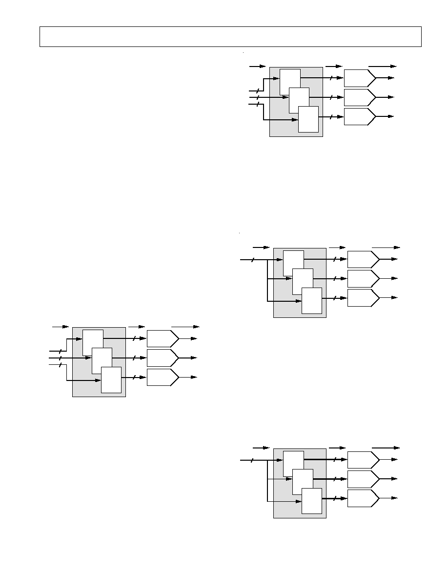
COLOR VIDEO MODES
The ADV7150 supports a number of color video modes all at
the maximum video rate.
Command bits CR24CR27 of Command Register 2 along with
Bit MR11 of Mode Register 1 determine the color mode.
24-Bit "Gamma" True Color
(CR25, CR26, CR27 = 1, 1, 1 and MR11 = 1)
The part is set to 24-bit/30-bit True-Color operation. The pixel
port accepts 24 bits of color data which is directly mapped to
the Look-Up Table RAM. The Look-Up Table is configured as
a 256 location by 30 bits deep RAM (10 bits each for Red,
Green and Blue). The output of the RAM drives the DACs with
30-bit data (10 bits each for Red, Green and Blue). The RAM is
preloaded with a user determined, nonlinear function, such as a
gamma correction curve.
10
10-BIT
RED DAC
10-BIT
BLUE DAC
RED
256 x 10
GREEN
256 x 10
BLUE
256 x 10
8
10-BIT
GREEN DAC
10
10
8
8
24-BIT
COLOR DATA
24-BIT TO 30-BIT
LOOK-UP TABLE
30-BIT
COLOR DATA
ANALOG VIDEO
OUTPUTS
RED
OUT
GREEN
OUT
BLUE
OUT
Figure 19. 24-Bit to 30-Bit True-Color Configuration
This mode allows for the display of full 24-bit, Gamma-
Corrected True-Color Images.
24-Bit "Standard" True Color
(CR25, CR26, CR27 = 1, 1, 1 and MR11 = 0)
This mode sets the part into direct 24-bit True-Color operation.
The pixel port accepts 24 bits of color data which is directly
mapped to Look-Up Table RAM. The Look-Up Table is con-
figured as a 256 location by 24 bits deep RAM (8 bits each for
Red, Green and Blue) and essentially acts as a bypass RAM.
The output of the RAM drives the DACs with 24-bit data (8
bits each for Red, Green and Blue). The RAM is preloaded with
a linear function.
This mode allows for the display of full 24-bit True-Color
Images.
8
8-BIT
RED DAC
8-BIT
BLUE DAC
RED
256 x 8
GREEN
256 x 8
BLUE
256 x 8
8
8-BIT
GREEN DAC
8
8
8
8
RED
OUT
GREEN
OUT
BLUE
OUT
24-BIT
COLOR DATA
24-BIT TO 24-BIT
LOOK-UP TABLE
24-BIT
COLOR DATA
ANALOG VIDEO
OUTPUTS
Figure 20. 24-Bit to 24-Bit Direct True-Color Configuration
8-Bit "Gamma" Pseudo Color
(CR25, CR26, CR27 = X, 0, 0 or X, 1, 0 or X, 0, 1 and
MR11 = 1)
This mode sets the part into 8-bit Pseudo-Color operation. The
pixel port accepts 8 bits of pixel data which indexes a 30-bit
word in the Look-Up Table RAM. The Look-Up Table is con-
figured as a 256 location by 30 bits deep RAM (10 bits each for
Red, Green and Blue). The output of the RAM drives the
DACs with 30-bit data (10 bits each for Red, Green and Blue).
10
10-BIT
RED DAC
10-BIT
BLUE DAC
RED
256 x 10
GREEN
256 x 10
BLUE
256 x 10
10-BIT
GREEN DAC
10
10
8
RED
OUT
GREEN
OUT
BLUE
OUT
8-BIT PIXEL
DATA
8-BIT TO 30-BIT
LOOK-UP TABLE
30-BIT
COLOR DATA
ANALOG VIDEO
OUTPUTS
Figure 21. 8-Bit to 30-Bit Pseudo-Color Configuration
This mode allows for the display of 256 simultaneous colors out
of a total palette of millions of addressable colors.
8-Bit "Standard" Pseudo Color
(CR25, CR26, CR27 = X, 0, 0 or X, 1, 0 or X, 0, 1 and
MR11 = 0)
This mode sets the part into 8-bit Pseudo-Color operation. The
pixel port accepts 8 bits of pixel data which indexes a 24-bit
word in the Look-Up Table RAM. The Look-Up Table is con-
figured as a 256 location by 24 bits deep RAM (10 bits each for
Red, Green and Blue). The output of the RAM drives the
DACs with 24-bit data (8 bits each for Red, Green and Blue).
8
8-BIT
RED DAC
8-BIT
BLUE DAC
RED
256 x 8
GREEN
256 x 8
BLUE
256 x 8
8-BIT
GREEN DAC
8
8
8
RED
OUT
GREEN
OUT
BLUE
OUT
8-BIT PIXEL
DATA
8-BIT TO 24-BIT
LOOK-UP TABLE
24-BIT
COLOR DATA
ANALOG VIDEO
OUTPUTS
Figure 22. 8-Bit to 24-Bit Pseudo-Color Configuration
This mode allows for the display of 256 simultaneous colors out
of a total palette of millions of addressable colors.
ADV7150
16
REV. A
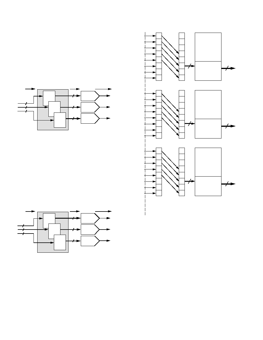
15-Bit "Gamma" True Color
(CR24, CR25, CR26, CR27 = 0, 0, 1, 1 or 1, 0, 1, 1 and
MR11 = 1)
The part is set to 15-bit True-Color operation. The pixel port
accepts 15-bits of color data which is mapped to the 5 LSBs of
each of the red, green and blue palettes of the Look-Up Table
RAM. The Look-Up Table is configured as a 32 location by
30 bits deep RAM (10 bits each for Red, Green and Blue). The
output of the RAM drives the DACs with 30-bit data (10 bits
each for Red, Green and Blue).
10
10-BIT
RED DAC
10-BIT
BLUE DAC
RED
32 x 10
GREEN
32 x 10
BLUE
32 x 10
5
10-BIT
GREEN DAC
10
10
5
5
RED
OUT
GREEN
OUT
BLUE
OUT
15-BIT
COLOR DATA
15-BIT TO 30-BIT
LOOK-UP TABLE
30-BIT
COLOR DATA
ANALOG VIDEO
OUTPUTS
Figure 23. 15-Bit to 30-Bit True-Color Configuration
This mode allows for the display of 15-bit, Gamma-Corrected
True-Color Images.
15-Bit "Standard" True Color
(CR24, CR25, CR26, CR27 = 0, 0, 1, 1 or 1, 0, 1, 1 and
MR11 = 0)
The part is set to 15-bit True-Color operation. The pixel port
accepts 15 bits of color data which is mapped to the 5 LSBs of
each of the red, green and blue palettes of the Look-Up Table
RAM. The Look-Up Table is configured as a 32 location by
24 bits deep RAM (8 bits each for Red, Green and Blue). The
output of the RAM drives the DACs with 24-bit data (8 bits
each for Red, Green and Blue).
8
8-BIT
RED DAC
8-BIT
BLUE DAC
RED
32 x 8
GREEN
32 x 8
BLUE
32 x 8
5
8-BIT
GREEN DAC
8
8
5
5
RED
OUT
GREEN
OUT
BLUE
OUT
15-BIT
COLOR DATA
15-BIT TO 24-BIT
LOOK-UP TABLE
24-BIT
COLOR DATA
ANALOG VIDEO
OUTPUTS
Figure 24. 15-Bit to 24-Bit True-Color Configuration
R4
R3
R2
R1
R0
x
x
x
G1
G0
G4
x
G3
G2
x
x
x
x
x
B4
B3
B2
B1
B0
PIXEL
INPUT
DATA
LOCATION "0"
LOCATION "31"
256 x 10
RAM
(RED LUT)
10
TO
RED
DAC
0
0
0
R4
R3
R2
R1
R0
LOCATION "0"
LOCATION "31"
256 x 10
RAM
(GREEN LUT)
10
TO
GREEN
DAC
0
0
0
G4
G3
G2
G1
G0
LOCATION "0"
LOCATION "31"
256 x 10
RAM
(BLUE LUT)
10
TO
BLUE
DAC
0
0
0
B4
B3
B2
B1
B0
5
5
5
PIN
ASSIGN-
MENTS
DATA
LATCHED
TO
PIXEL
PORT
DATA LATCHES
FIRST 32
LOCATIONS
OF RAM
DATA
INTERNALLY
SHIFTED
TO 5 LSBS
B5
B4
B3
B2
B1
B0
x
x
x
x
x
x
x
x
B6
B7
G6
G5
G4
G3
G2
G1
G0
R6
R5
R4
R3
R2
R1
R0
R4
R3
R2
R1
R0
G4
G3
G2
x
G1
G0
B4
B3
B2
B1
B0
G7
R7
Figure 25. 15-Bit True-Color Mapping Using R3R7,
G3G7 and B3B7
This mode allows for the display of 15-bit True-Color Images.
PIXEL PORT MAPPING
The pixel data to the ADV7150 is automatically mapped in the
parts pixel port as determined by the pixel data mode pro-
grammed (Bits CR24CR27 of Command Register 2).
Pixel data in the 24-bit True-Color modes is directly mapped to
the 24 color inputs R0R7, G0G7 and B0B7.
There are three modes of operation for 8-bit Pseudo Color.
Each mode maps the input pixel data differently. Data can be
input one of the three color channels, R0R7 or G0G7 or
B0B7.
ADV7150
17
REV. A
R4
R3
R2
R1
R0
G4
G2
G3
x
G1
G0
G4
B4
B3
B2
B1
x
x
x
x
x
x
x
x
PIXEL
INPUT
DATA
LOCATION "0"
LOCATION "31"
256 x 10
RAM
(RED LUT)
10
TO
RED
DAC
0
0
0
R4
R3
R2
R1
R0
LOCATION "0"
LOCATION "31"
256 x 10
RAM
(GREEN LUT)
10
TO
GREEN
DAC
0
0
0
G4
G3
G2
G1
G0
LOCATION "0"
LOCATION "31"
256 x 10
RAM
(BLUE LUT)
10
TO
BLUE
DAC
0
0
0
B4
B3
B2
B1
B0
5
5
5
PIN
ASSIGN-
MENTS
DATA
LATCHED
TO
PIXEL
PORT
DATA LATCHES
FIRST 32
LOCATIONS
OF RAM
DATA
INTERNALLY
SHIFTED
TO 5 LSBS
B5
B4
B3
B2
B1
B0
x
x
x
x
x
x
x
x
B6
B7
G6
G5
G4
G3
G2
G1
G0
R6
R5
R4
R3
R2
R1
R0
R4
R3
R2
R1
R0
G4
G3
G2
x
G1
G0
B4
B3
B2
B1
B0
G7
R7
Figure 26. 15-Bit True-Color Mapping Using R0R7 and
G0G6
The part has two modes of operation for 15-bit True Color. In
the first mode, data is input to the device over the red, green
and blue channel (R3R7, G3G7 and B3B7) and is internally
mapped to locations 0 to 31 of the Look-Up Table (LUT) ac-
cording to Figure 25. In the second mode, data is input to the
device over just two of the color ports, red and green (R0R7
and G0G6) and is internally mapped to LUT locations 0 to 31
according to Figure 26. (Note: Data on unused pixel inputs is
ignored.)
MICROPROCESSOR (MPU) PORT
The ADV7150 supports a standard MPU Interface. All the
functions of the part are controlled via this MPU port. Direct
access is gained to the Address Register, Mode Register and all
the Control Registers as well as the Color Palette. The following
sections describe the setup for reading and writing to all of the
devices registers.
MPU Interface
The MPU interface (Figure 27) consists of a bidirectional,
10-bit wide databus and interface control signals CE, C0, C1
and R/W. The 10-bit wide databus is user configurable as
illustrated.
Table II. Databus Width Table
Databus
RAM/DAC
Read/Write
Width
Resolution
Mode
10-Bit
10-Bit
10-Bit Parallel
10-Bit
8-Bit
8-Bit Parallel
8-Bit
10-Bit
8+2 Byte
8-Bit
8-Bit
8-Bit Parallel
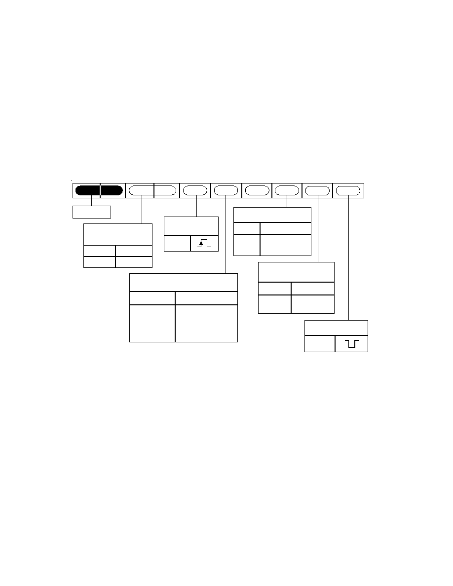
Register Mapping
The ADV7150 contains a number of onboard registers includ-
ing the Mode Register (MR17MR10), Address Register (A7
A0) and nine Control Registers as well as Red (R9R0), Green
(G9G0) and Blue (B9B0) Color Registers. These registers
control the entire operation of the part. Figure 28 shows the
internal register configuration.
Control lines C1 and C0 determine which register the MPU is
accessing. C1 and C0 also determine whether the Address Reg-
ister is pointing to the color registers and look-up table RAM or
the control registers. If C1, C0 = 1, 0 the MPU has access to
whatever control register is pointed to by the Address Register
(A7A0). If C1, C0 = 0, 1 the MPU has access to the Look-Up
Table RAM (Color Palette) through the associated color regis-
ters. The CE input latches data to or from the part.
The R/W control input determines between read or write ac-
cesses. The Truth Tables III and IV show all modes of access to
the various registers and color palette for both the 8-bit wide
databus configuration and 10-bit wide databus configuration. It
should be noted that after power-up, the devices MPU port is
automatically set to 10-bit wide operation (see Power-On Reset
section).
Color Palette Accesses
Data is written to the color palette by first writing to the address
register of the color palette location to be modified. The MPU
performs three successive write cycles for each of the red, green
and blue registers (10-bit or 8-bit). An internal pointer moves
from red to green to blue after each write is completed. This
pointer is reset to red after a blue write or whenever the address
register is written. During the blue write cycle, the three bytes of
red, green and blue are concatenated into a single 30-bit/24-bit
word and written to the RAM location as specified in the ad-
dress register (A7A0). The address register then automatically
increments to point to the next RAM location and a similar red,
green and blue palette write sequence is performed. The address
register resets to 00H following a blue write cycle to color pal-
ette RAM location FFH.
ADV7150
18
REV. A
30
MPU PORT
D9 D0
10 (8+2)
C0
C1
ADDR
(A7A0)
REVISION
REGISTER
COMMAND
REGISTERS
(CR1CR3)
TEST
REGISTERS
(MR1)
DATA TO
PALETTES
CONTROL REGISTERS
COLOR REGISTERS
ADDRESS
REGISTER
MODE
REGISTER
ID
REGISTER
BLUE
REGISTER
PIXEL MASK
REGISTER
CE
R/W
GREEN
REGISTER
RED
REGISTER
Figure 27. MPU Port and Register Configuration
Data is read from the color palette by first writing to the address
register of the color palette location to be read. The MPU per-
forms three successive read cycles from each of the red, green
and blue locations (10-bit or 8-bit) of the RAM. An internal
pointer moves from red to green to blue after each read is com-
pleted. This pointer is reset to red after a blue read or whenever
the address register is written. The address register then auto-
matically increments to point to the next RAM location, and a
similar red, green and blue palette read sequence is performed.
The address register resets to 00H following a blue read cycle of
color palette RAM location FFH.
Register Accesses
The MPU can write to or read from all of the ADV7150s regis-
ters. C0 and C1 determine whether the Mode Register or Ad-
dress Register is being accessed. Access to these registers is
direct. The Control Registers are accessed indirectly. The
Address Register must point to the desired Control Register.
Figure 28 along with the 8-bit and 10-bit Interface Truth Tables
illustrate the structure and protocol for device communication
over the MPU port.
MODE REGISTER
(MR17MR10)
ADDRESS REGISTER
(A7A0)
ADDRESS
REGISTER
(A15A0)
CONTROL
REGISTERS
00H
01H
02H
PIXEL TEST REGISTER
R G B
DAC TEST REGISTER
R G B
* THIS REGISTER IS READ ONLY.
A READ CYCLE WILL RETURN ZEROS "00".
LOOK-UP TABLE RAM
(256 x 30)
RED
REGISTER
(R9R0)
GREEN
REGISTER
(G9G0)
BLUE
REGISTER
(B9B0)
POINTS TO LOCATION
CORRESPONDING TO
ADDRESS REG (A7A0)
ADDRESS REG = ADDRESS REG + 1
C1 = 1
C0 = 0
C1 = 0
C0 = 1
C1 = 1
C0 = 1
C1 = 0
C0 = 0
SYNC, BLANK & I
PLL
TEST REGISTER
03H
04H
05H
06H
07H
08H
09H
0AH
0BH
RESERVED* (READ ONLY)
RESERVED* (READ ONLY)
RESERVED* (READ ONLY)
REVISION REGISTER
ID REGISTER (READ ONLY)
PIXEL MASK REGISTER
COMMAND REGISTER 1
COMMAND REGISTER 2
COMMAND REGISTER 3
Figure 28. Internal Register Configuration and Address Decoding
ADV7150
19
REV. A
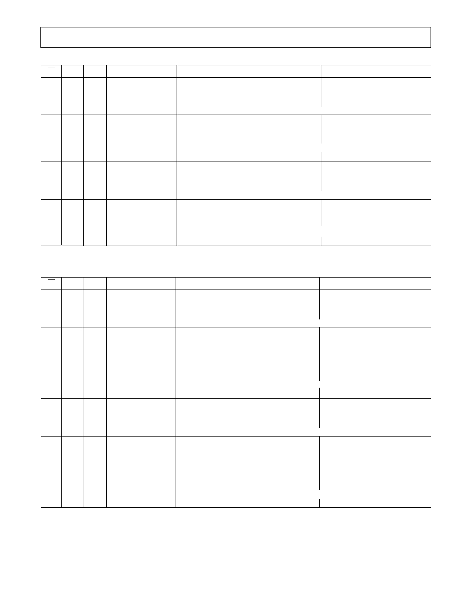
Table III. Interface Truth Table (10-Bit Databus Mode)
R/W
C1
C0
Databus (D9D0)
Operation
Result
0
1
1
DB7DB0
Write to Mode Register
DB7DB0 ¡ MR17MR10
0
0
0
DB7DB0
Write to Address Register
DB7DB0 ¡ A7A0
0
1
0
DB7DB0
Write to Control Registers
DB7DB0 ¡ Control Register
(Particular Control Register Determined by Address Register)
0
0
1
DB9DB0
Write to RED Register
DB9DB0 ¡ R9R0
0
0
1
DB9DB0
Write to GREEN Register
DB9DB0 ¡ G9G0
0
0
1
DB9DB0
Write to BLUE Register
DB9DB0 ¡ B9B0
Write RGB Data to RAM Location Pointed to by Address Register (A7A0)
Address Register = Address Register + 1
1
1
1
DB7DB0
Read Mode Register
MR17MR10 ¡ DB7DB0
1
0
0
DB7DB0
Read Address Register
A7A0 ¡ DB7DB0
1
1
0
DB7DB0
Read Control Registers
Register Data ¡ DB7DB0
(Particular Control Register Determined by Address Register)
1
0
1
DB9DB0
Read RED RAM Location
R9R0 ¡ DB9DB0
1
0
1
DB9DB0
Read GREEN RAM Location
G9G0¡ DB9DB0
1
0
1
DB9DB0
Read BLUE RAM Location
B9B0 ¡ DB9DB0
(RAM Location Pointed to by Address Register(A7A0))
Address Register = Address Register + 1
DB = Data Bit.
Table IV. Interface Truth Table (8-Bit Databus Mode)*
R/W
C1
C0
Databus (D7D0)
Operation
Result
0
1
1
DB7DB0
Write to Mode Register
DB7DB0 ¡ MR17MR10
0
0
0
DB7DB0
Write to Address Register
DB7DB0 ¡ A7A0
0
1
0
DB7DB0
Write to Control Registers
DB7DB0 ¡ Control Registers
(Particular Control Register Determined by Address Register (A7A0))
0
0
1
DB9DB2
Write to RED Register
DB9DB2 ¡ R9R2
0
0
1
DB1DB0
Write to RED Register
DB1DB0 ¡ R1R0
0
0
1
DB9DB2
Write to GREEN Register
DB9DB2 ¡ G9G2
0
0
1
DB1DB0
Write to GREEN Register
DB1DB0 ¡ G1G0
0
0
1
DB9DB2
Write to BLUE Register
DB9DB2 ¡ B9B2
0
0
1
DB1DB0
Write to BLUE Register
DB1DB0 ¡ B1B0
Write RGB Data to RAM Location Pointed to by Address Register (A7-A0)
Address Register = Address Register + 1
1
1
1
DB7DB0
Read Mode Register
MR17MR10 ¡ DB7DB0
1
0
0
DB7DB0
Read Address Register
A7A0 ¡ DB7DB0
1
1
0
DB7DB0
Read Control Registers
Register Data ¡ DB7DB0
(Particular Control Register Determined by Address Register)
1
0
1
DB9DB2
Read RED RAM Location
R9R2 ¡ DB9DB2
1
0
1
DB1DB0
Read RED RAM Location
R1R0 ¡ DB1DB0
1
0
1
DB9DB2
Read GREEN RAM Location
G9G2 ¡ DB9DB2
1
0
1
DB1DB0
Read GREEN RAM Location
G1G0 ¡ DB1DB0
1
0
1
DB9DB2
Read BLUE RAM Location
B9B2 ¡ DB9DB2
1
0
1
DB1DB0
Read BLUE RAM Location
B1B0 ¡ DB1DB0
(RAM Location Pointed to by Address Register (A7A0))
Address Register = Address Register + 1
*Writing or reading 10-bit data (DB9DB0) over an 8-bit databus (D7D0) requires two write or two read cycles.
:DB9DB2 is mapped to D7D0 on the first cycle.
:DB1DB0 is mapped to D1D0 on the second cycle.
DB = Data Bit.
ADV7150
20
REV. A
Power-On Reset
On power-up of the ADV7150 executes a power-on reset opera-
tion. This initializes the pixel port such that the pixel sequence
ABCD starts at A. The Mode Register (MR17MR10), Com-
mand Register 2 (CR27CR20) and Command Register 3
(CR37CR30) have all bits set to a Logic "1." Command Regis-
ter 1 (CR17CR10) has all bits set to a Logic "0."
The output clocking signals are also set during this reset period.
PRGCKOUT = CLOCK/32
LOADOUT = CLOCK/4
The power-on reset is activated when V
AA
goes from 0 V to
5 V. This reset is active for 1
µ
s. The ADV7150 should not be
accessed during this reset period. The pixel clock should be
applied at power-up.
REGISTER PROGRAMMING
The following section describes each register, including Address
Register, Mode Register and each of the nine Control Registers
in terms of its configuration.
Address Register (A7A0)
As illustrated in the previous tables, the C0 and C1 control in-
puts, in conjunction with this address register specify which
control register, or color palette location is accessed by the
MPU port. The address register is 8-bits wide and can be read
from as well as written to. When writing to or reading from the
color palette on a sequential basis, only the start address needs
to be written. After a red, green and blue write sequence, the
address register is automatically incremented.
MODE REGISTER MR1 (MR19MR10)
The mode register is a 10-bit wide register. However for pro-
gramming purposes, it may be considered as an 8-bit wide regis-
ter (MR18 and MR19 are both reserved). It is denoted as
MR17MR10 for simplification purposes.
The diagram shows the various operations under the control of
the mode register. This register can be read from as well written
to. In read mode, if MR18 and MR19 are read back, they are
both returned as zeros.
Mode Register (MR17MR10) Bit Description
Reset Control (MR10)
This bit is used to reset the pixel port sampling sequence. This
ensures that the pixel sequence ABCD starts at A. It is reset by
writing a "1" followed by a "0" followed by a "1." This bit must
be run through this cycle during the initialization sequence.
RAM-DAC Resolution Control (MR11)
When this is programmed with a "1," the RAM is 30 bits deep
(10 bits each for red, green and blue) and each of the three
DACs is configured for 10-bit resolution. When MR11 is
programmed with a "0," the RAM is 24-bits deep (8 bits each
for red, green and blue) and the DACs are configured for 8-bit
resolution. The two LSBs of the 10-bit DACs are pulled down
to zero in 8-bit RAM-DAC mode.
MPU Databus Width (MR12)
This bit determines the width of the MPU port. It is configured
as either a 10-bit wide (D9D0) or 8-bit wide (D7D0) bus.
10-bit data can be written to the device when configured in
8-bit wide mode. The 8 MSBs are first written on D7D0, then
the two LSBs are written over D1D0. Bits D9D8 are zeros in
8-bit mode.
Operational Mode Control (MR14MR13)
When MR14 is "0" and MR13 is "1," the part operates in
normal mode.
Calibrate LOADIN (MR15)
This bit automatically calibrates the onboard LOADIN/
LOADOUT synchronization circuit. A "0" to "1" transition
initiates calibration. This bit is set to "0" in normal operation.
See "Pipeline Delay and Calibration" section. This bit must be
run through this cycle during the initialization sequence.
MR17
MR16
* THESE BITS ARE READ-ONLY RESERVED BITS.
A READ CYCLE WILL RETURN ZEROS "00."
RESERVED*
MR16 PS0
MR17 PS1
PALETTE SELECT
MATCH BITS CONTROL
RAM-DAC
RESOLUTION CONTROL
0 8-BIT
1 10-BIT
MR11
MPU DATA BUS WIDTH
0 8-BIT (D7D0)
1 10-BIT (D9D0)
MR12
CALIBRATE
LOADIN
MR15
RESET CONTROL
MR10
OPERATIONAL MODE CONTROL
0 0 RESERVED
0 1 NORMAL OPERATION
1 0 RESERVED
1 1 RESERVED
MR14 MR13
MR19
MR18
MR15
MR14
MR13
MR12
MR11
MR10
Mode Register 1 (MR1) (MR19MR10)
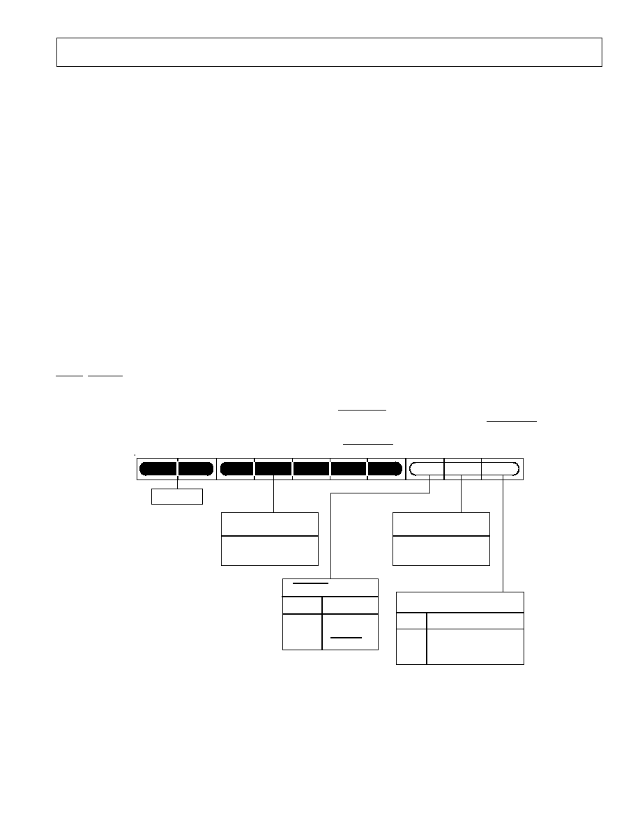
ADV7150
21
REV. A
Palette Select Match Bits Control (MR17MR16)
These bits allow multiple palette devices to work together.
When bits PS1 and PS0 match MR17 and MR16 respectively,
the device is selected. If these bits do not match, the device is
not selected and the analog video outputs drive 0 mA, see
"Palette Priority Select Inputs" section.
CONTROL REGISTERS
The ADV7150 has 9 control registers. To access each register,
two write operations must be performed. The first write to the
address register specifies which of the 9 registers is to be ac-
cessed. The second access determines the value written to that
particular control register.
Pixel Test Register
(Address Reg (A7A0) = 00H)
This register is used when the device is in test/diagnostic mode.
It is a 24-bit (8 bits each for RED, GREEN and BLUE) wide
read-only register which allows the MPU to read data on the
pixel port, see "Test Diagnostic" section.
DAC Test Register
(Address Reg (A7A0) = 01H)
This register is used when the device is in test/diagnostic mode.
It is a 30-bit (10 bits each for RED, GREEN and BLUE) wide
read-only register which allows MPU access to the DAC port,
see "Test Diagnostic" section.
SYNC
, BLANK and I
PLL
Test Register
(Address Reg (A7A0) = 02H)
This register is used when the device is in test/diagnostic mode.
It is a 3-bit wide (3 LSBs) read/write register which allows MPU
access to these particular pixel control bits, see "Test Diagnos-
tic" section.
ID Register
(Address Reg (A7A0) = 03H)
This is an 8-bit wide "Identification" read-only register. For the
ADV7150 it will always return the hexadecimal value 8EH.
Pixel Mask Register
(Address Reg (A7A0) = 04H)
The contents of the pixel mask register are individually bit-wise
logically AND-ed with the Red, Green and Blue pixel input
stream of data. It is an 8-bit read/write register with D0 corre-
sponding to R0, G0 and B0. For normal operation, this register
is set with FFH.
COMMAND REGISTER 1 (CR1)
(Address Reg (A7A0) = 05H)
This register contains a number of control bits as shown in the
diagram. CR1 is a 10-bit wide register. However for program-
ming purposes, it may be considered as an 8-bit wide register
(CR18 to CR19 are reserved).
The diagram below shows the various operations under the con-
trol of CR1. This register can be read from as well as written to. In
write mode, "0" should be written to CR11 and CR13 to CR17.
In read mode, CR11 and CR13 to CR19 are returned as zeros.
COMMAND REGISTER 1-BIT DESCRIPTION
Calibration Control (CR10)
This bit automatically calibrates the onboard LOADIN/
LOADOUT synchronization circuit. MR15 of Mode Register
MR1 must be set to "0."
SYNCOUT
Control (CR12)
This bit specified whether the video SYNCOUT signal is to be
enabled. On power up a "0" is written to the bit and
"SYNCOUT" is set three-state.
*THESE BITS ARE
READONLY
RESERVED BITS.
A READ CYCLE WILL
RETURN ZEROS "00."
CR12
0 DISABLE
1 ENABLE
SYNCOUT
SYNCOUT CONTROL
CR17
CR16
CR15
CR14
CR12
CR11
CR10
CR13
RESERVED*
CR11
(0)
THIS BIT SHOULD BE
SET TO ZERO
CALIBRATION CONTROL
CR10
0
1
DISABLE
CALIBRATES ON EVERY
VERTICAL SYNC (MR15=0)
CR17-CR13
(00000)
THESE BITS SHOULD
BE SET TO ZERO
CR18
CR19
Command Register 1 (CR1) (CR19CR10)
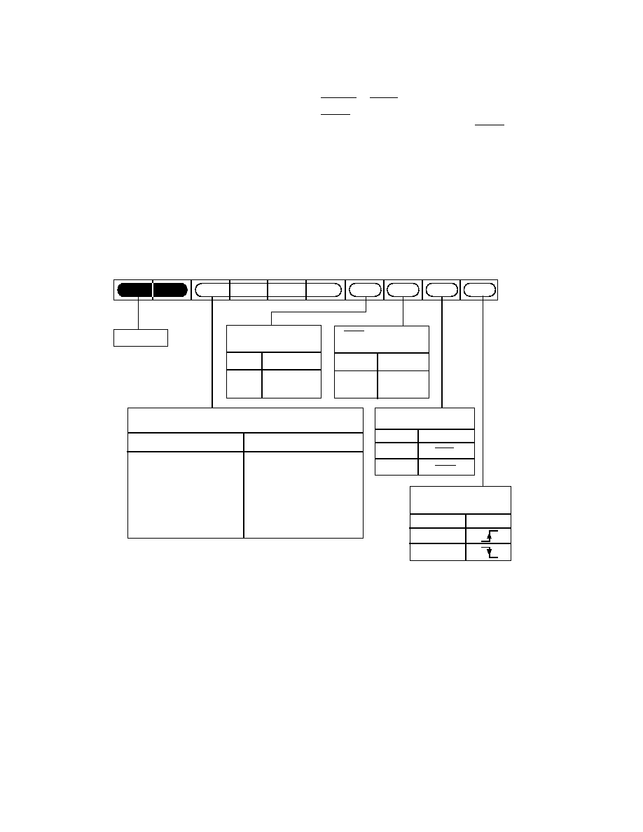
ADV7150
22
REV. A
COMMAND REGISTER 2 (CR2)
(Address Reg (A7A0) = 06H)
This register contains a number of control bits as shown in the
diagram. CR2 is a 10-bit wide register. However, for program-
ming purposes, it may be considered as an 8-bit wide register
(CR28 and CR29 are both reserved).
The diagram shows the various operations under the control of
CR2. This register can be read from as well written to. In read
mode, CR28 and CR29 are both returned as zeros.
COMMAND REGISTER 2-BIT DESCRIPTION
R7 Trigger Polarity Control (CR20)
This bit is used when the device is in test/diagnostic mode. It
determines whether the pixel data is latched into the test regis-
ters in the rising or falling edge of R7. (See "Test Diagnostics"
section.)
I
PLL
Trigger Control (CR21)
This bit specifies whether the I
PLL
output is triggered from
BLANK
or SYNC.
SYNC
Recognition Control (CR22)
This bit specifies whether the video SYNC input is to be
encoded onto the IOG analog output or ignored.
Pedestal Enable Control (CR23)
This bit specifies whether a 0 IRE or a 7.5 IRE blanking pedes-
tal is to be generated on the video outputs.
True-Color/Pseudo-Color Mode Control (CR27CR24)
These 4 bits specify the various color modes. These include a
24-bit true-color mode, two 15-bit true-color modes and three
8-bit pseudo color modes.
CR20
RESERVED*
CR26
CR25
CR24
CR27
0
1
CR21
I
PLL
TRIGGER CONTROL
SYNC
BLANK
R7 TRIGGER
POLARITY CONTROL
0
1
CR20
CR29
CR28
CR22
0
IGNORE
1
DECODE
SYNC RECOGNITION
CONTROL
*THESE BITS ARE READ-
ONLY RESERVED BITS.
A READ CYCLE WILL
RETURN ZEROS "00."
CR21
CR23
CR22
TRUE COLOR/PSEUDO-COLOR MODE CONTROL
MODE
0
1
1
1
1
0
0
0
1
0
0
0
1
1
0
1
CR27
CR26
CR24
CR25
1
1
0
0
0
0
0
0
8-BIT PSEUDO COLOR ON R7R0
8-BIT PSEUDO COLOR ON G7G0
8-BIT PSEUDO COLOR ON B7B0
15-BIT TRUE COLOR ON
R7R3, G7G3, B7B3
15-BIT TRUE COLOR ON
R7R0, G6G0
24-BIT TRUE COLOR
R7R0, G7G0, B7B0
PEDESTAL ENABLE
CONTROL
CR23
0
0 IRE
1
7.5 IRE
Command Register 2 (CR2) (CR29CR20)
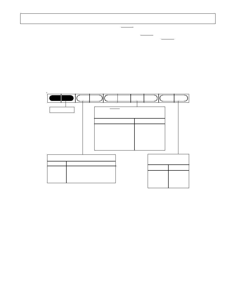
ADV7150
23
REV. A
COMMAND REGISTER 3 (CR3)
(Address Reg (A7A0) = 07H)
This register contains a number of control bits as shown in the
diagram. CR3 is a 10-bit wide register. However for program-
ming purposes, it may be considered as an 8-bit wide register
(CR38 and CR39 are both reserved).
The diagram shows the various operations under the control of
CR3. This register can be read from as well written to. In read
mode, CR38 and CR39 are both returned as zeros.
COMMAND REGISTER 3-BIT DESCRIPTION
PRGCKOUT Frequency Control (CR31CR30)
These bits specify the output frequency of the PRGCKOUT
output. PRGCKOUT is a divided down version of the pixel
CLOCK.
BLANK
Pipeline Delay Control (CR35CR32)
These bits specify the additional pipeline delay that can be
added to the BLANK function, relative to the overall device
pipeline delay (t
PD
). As the BLANK control normally enters the
video DAC from a shorter pipeline than the video pixel data,
this control is useful in deskewing the pipeline differential.
Pixel Multiplex Control (CR37CR36)
These bits specify the device's multiplex mode. It, therefore,
also determines the frequency of the LOADOUT signal.
LOADOUT is a divided down version of the pixel CLOCK.
Revision Register
(Address Reg (A7A0) = 0BH)
This register is a read only register containing the revision of
silicon.
CR39
CR38
CR37
CR36
CR35
CR34
CR32
CR31
CR30
CR33
*THESE BITS ARE READ-
ONLY RESERVED BITS.
A READ CYCLE WILL
RETURN ZEROS "00."
PRGCKOUT FREQUENCY
CONTROL
CR31 CR30
0
0
1
1
0
1
0
1
CLOCK
÷
4
CLOCK
÷
8
CLOCK
÷
16
CLOCK
÷
32
RESERVED*
PIXEL MULTIPLEX CONTROL
CR37 CR36
0
0
1
1
0
1
0
1
1:1 MUXING: LOADOUT = CLOCK
÷
1
2:1 MUXING LOADOUT = CLOCK
÷
2
RESERVED
4:1 MUXING :LOADOUT = CLOCK
÷
4
EXTRA BLANK PIPELINE DELAY CONTROL
(ADDS TO PIXEL PIPELINE DELAY; t
PD
)
CR35 CR34 CR33 CR32
0
0
0
1
0
1
0
1
0
0
1
1
0
0
0
1
t
PD
t
PD
+ 1 x LOADOUT
t
PD
+ 2 x LOADOUT
t
PD
+ 15 x LOADOUT
·
·
·
·
·
·
·
·
·
·
Command Register 3 (CR3) (CR39CR30)
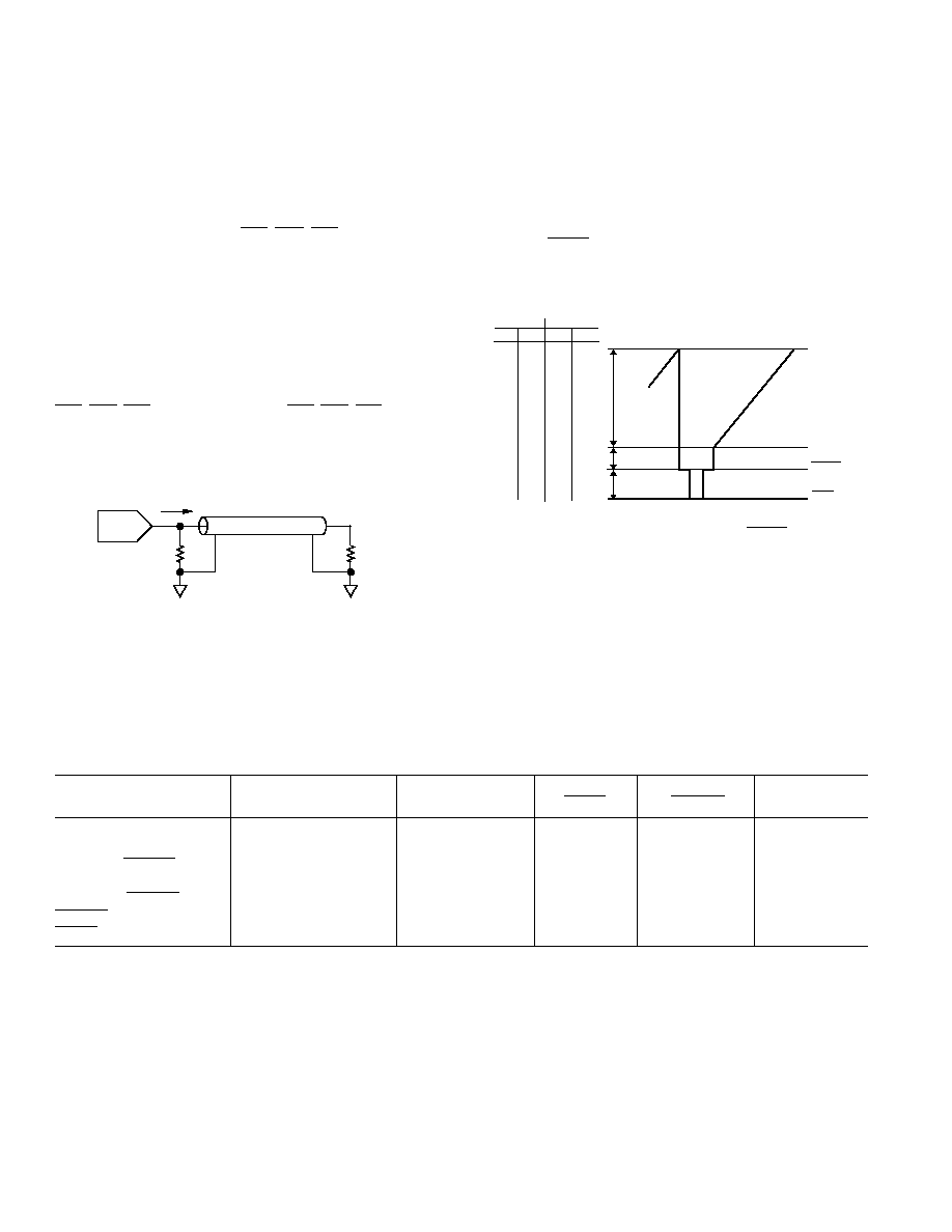
ADV7150
24
REV. A
DIGITAL-TO-ANALOG CONVERTERS
(DACS) AND VIDEO OUTPUTS
The ADV7150 contains three high speed video DACs. The
DAC outputs are represented as the three primary analog color
signals IOR (red video), IOG (green video) and IOB (blue video).
Other analog signals on the part include I
PLL
and V
REF
as well as
complementary video outputs IOR, IOG, IOB. These comple-
mentary outputs can be used to drive differentially terminated
video loads, they will have equal but opposite output levels to
IOR, IOG and IOB when loaded with a resistive load similar to
IOR, IOG and IOB.
DACs and Analog Outputs
The part contains three matched 10-bit digital-to-analog con-
verters. The DACs are designed using an advanced, high speed,
segmented architecture. The bit currents corresponding to each
digital input are routed to either IOR, IOG, IOB (bit = "l") or
IOR
, IOG, IOB (bit = "0"). (Normally IOR, IOG, IOB = GND.)
The analog video outputs are high impedance current sources.
Each of the these three RGB current outputs are specified to
directly drive a 37.5
load (doubly terminated 75
).
DACs
IOR, IOG, IOB
ZO = 75
ZS = 75
(SOURCE
TERMINATION)
ZL = 75
(MONITOR)
(CABLE)
Figure 29. DAC Output Termination (Doubly Terminated
75
Load)
Reference Input and R
SET
An external 1.23 V voltage reference is required to drive the
analog outputs of the ADV7150. The reference voltage is con-
nected to the V
REF
input.
A resistor R
SET
is connected between the R
SET
input of the part
and ground. For specified performance, R
SET
has a value of
280
. This corresponds to the generation of RS-343A video
levels (with SYNC on IOG and Pedestal = 7.5 IRE) into a dou-
bly terminated 75
load. Figure 30 illustrates the resulting
video waveform, and the Video Output Truth Table shows the
corresponding control input stimuli.
WHITE
LEVEL
IOR, IOB
IOG
mA
mA
V
V
26.67
1.000
0.714
19.05
0
0
0
0
7.62
0.286
BLANK
LEVEL
SYNC
LEVEL
GRAY SCALE
92.5 IRE
7.5 IRE
40 IRE
BLACK
LEVEL
1.44
0.054
9.05
0.340
Figure 30. Composite Video Waveform (SYNC Decoded
on IOG; Pedestal = 7.5 IRE; R
SET
= 280
)
Variations on RS-343A
Various other video output configurations can be implemented
by the ADV7150, including RS-170. Values of R
SET
for particu-
lar output video formats/levels are calculated by using the equa-
tions for R
SET
given in the "Pin Configuration" section. The
table shows calculated values of R
SET
for some of the most com-
mon variants on the RS-343A standard. The associated wave-
forms are shown in the diagrams.
Table V. Video Output Truth Table
IOG
IOR, IOB
DAC
Description
(mA)
(mA)
SYNC
BLANK
Input Data
WHITE LEVEL
26.67
19.05
1
1
3FFH
VIDEO
Video + 9.05
Video + 1.44
1
1
Data
VIDEO to BLANK
Video + 1.44
Video + 1.44
0
1
Data
BLACK LEVEL
9.05
1.44
1
1
000H
BLACK to BLANK
1.44
1.44
0
1
000H
BLANK
LEVEL
7.62
0
1
0
xxxH
SYNC
LEVEL
0
0
0
0
xxxH
Decoded on IOG; Pedestal = 0 IRE; R
SET
= 265
.
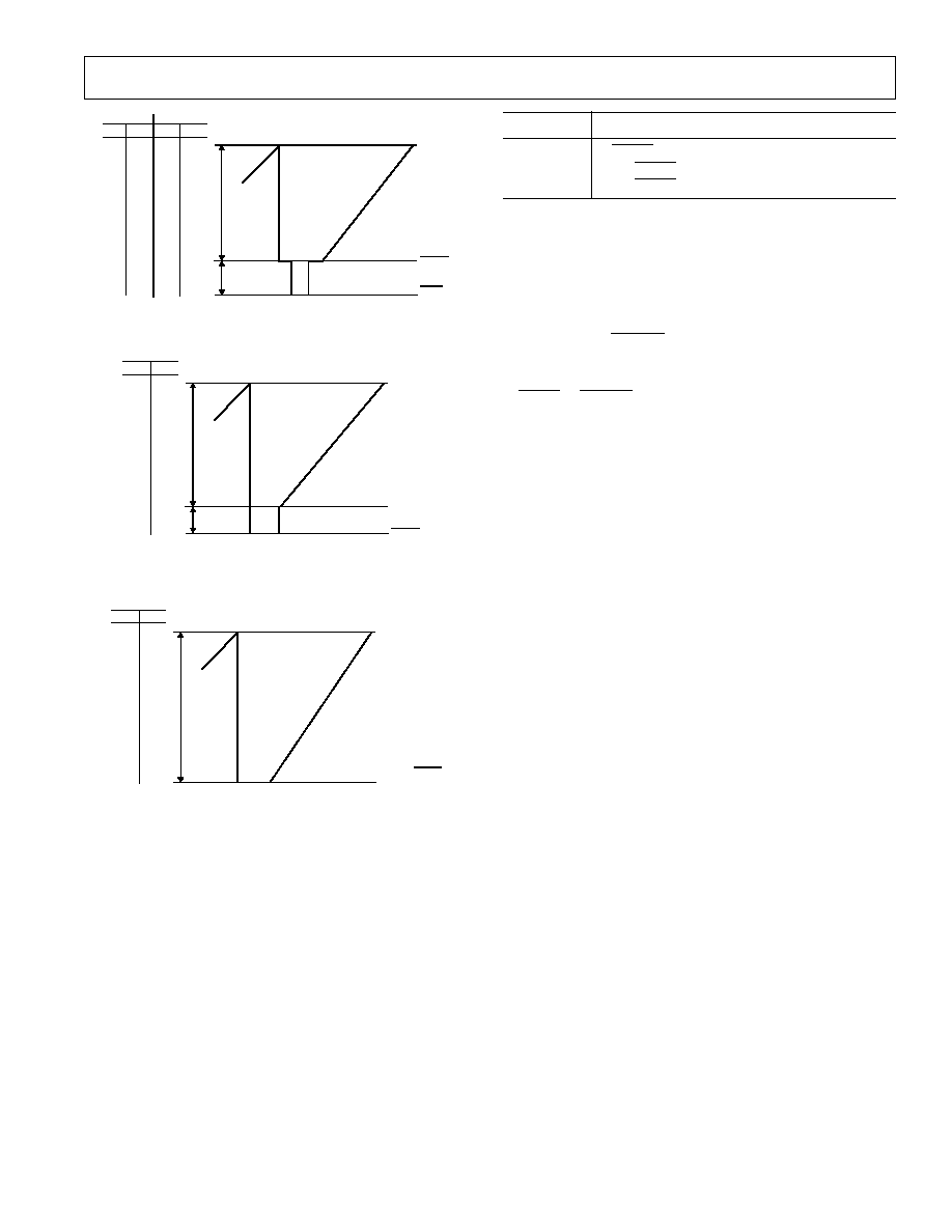
ADV7150
25
REV. A
WHITE
LEVEL
100 IRE
43 IRE
IOR, IOB
IOG
mA
mA
V
V
26.67
1.000
0.698
18.62
0
0
0
0
8.05
0.302
BLACK/
BLANK
LEVEL
SYNC
LEVEL
GRAY SCALE
Figure 31. Composite Video Waveform SYNC
WHITE LEVEL
BLACK LEVEL
92.5 IRE
7.5 IRE
IOR, IOB, IOG
mA
V
19.05
0.714
0
0
1.44
0.054
BLANK LEVEL
GRAY SCALE
Figure 32. Composite Video Waveform
(Pedestal = 7.5 IRE; R
SET
= 280
)
WHITE LEVEL
100 IRE
IOR, IOB, IOG
mA
V
19.05
0.714
0
0
BLACK/ BLANK
LEVEL
GRAY SCALE
Figure 33. Composite Video Waveform
(Pedestal = 0 IRE; R
SET
= 259
)
R
SET
( )
Video Signal
265
SYNC
decoded on IOG; Pedestal = 0 IRE
280
No SYNC decoded; Pedestal = 7.5 IRE
259
No SYNC decoded; Pedestal = 0 IRE
I
PLL
Synchronization Output Control
This output synchronization signal is used in applications where
it is necessary to synchronize multiple palette devices (ADV7150
+ ADV7151) to subpixel resolution. Each devices I
PLL
output
signal is in phase with its analog RGB output signal. If multiple
devices have differing output delays, the time difference can be
derived from the I
PLL
signals. This time difference is then used
to phase shift the CLOCK inputs on one or other of the devices
inputs.
The I
PLL
signal is internally triggered by either the falling edge
of SYNC or BLANK as determined by CR21 of Command
Register 2.
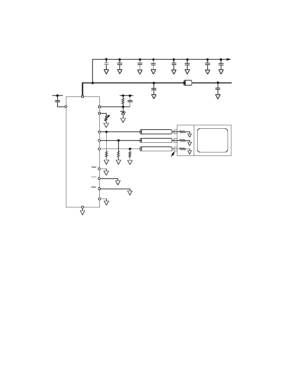
ADV7150
26
REV. A
APPENDIX 1
BOARD DESIGN AND LAYOUT CONSIDERATIONS
V
AA
V
REF
R
SET
IOR
IOG
IOB
I
PLL
GND
COMP
IOR
IOG
IOB
R
SET
280
1k
(1% METAL)
AD589
(1.2V REF)
0.1
µ
F
+5V (V
AA
)
75
75
75
75
75
75
COMPLIMENTARY
OUTPUTS
CO-AXIAL CABLE
(75
)
BNC
CONNECTORS
MONITOR
(CRT)
+5V (V
AA
)
0.1
µ
F
ANALOG POWER PLANE
33
µ
F
0.1
µ
F
0.01
µ
F
0.1
µ
F
0.01
µ
F
0.1
µ
F
0.01
µ
F
0.1
µ
F
0.01
µ
F
+5V (V
AA
)
0.1
µ
F
+5V (V
CC
)
L1
(FERRITE BEAD)
NOTES:
1. ALL RESISTORS ARE 1% METAL FILM
2. 0.1
µ
F AND 0.01
µ
F CAPACITORS ARE CERAMIC
3. ADDITIONAL DIGITALCIRCUITRY OMITTED FOR CLARITY
ADV7150
POWER SUPPLY DECOUPLING (0.1
µ
F AND 0.01
µ
F CAPACITOR FOR EACH V
AA
GROUP)
Recommended Analog Circuit Layout
power plane (V
CC
) at a single point through a ferrite bead. This
bead should be located within three inches of the ADV7150.
The PCB power plane should provide power to all digital logic
on the PC board, and the analog power plane should provide
power to all ADV7150 power pins and voltage reference circuitry.
Plane-to-plane noise coupling can be reduced by ensuring that
portions of the regular PCB power and ground planes do not
overlay portions of the analog power plane, unless they can be
arranged such that the plane-to-plane noise is common mode.
Supply Decoupling
For optimum performance, bypass capacitors should be installed
using the shortest leads possible, consistent with reliable opera-
tion, to reduce the lead inductance. Best performance is obtained
with 0.1
µ
F ceramic capacitor decoupling. Each group of V
AA
pins on the ADV7150 must have at least one 0.1
µ
F decoupling
capacitor to GND. These capacitors should be placed as close
as possible to the device.
It is important to note that while the ADV7150 contains cir-
cuitry to reject power supply noise, this rejection decreases with
frequency. If a high frequency switching power supply is used,
the designer should pay close attention to reducing power sup-
ply noise and consider using a three terminal voltage regulator
for supplying power to the analog power plane.
The ADV7150 is a highly integrated circuit containing both
precision analog and high speed digital circuitry. It has been
designed to minimize interference effects on the integrity of the
analog circuitry by the high speed digital circuitry. It is impera-
tive that these same design and layout techniques be applied to
the system level design such that high speed, accurate perfor-
mance is achieved. The "Recommended Analog Circuit Layout"
shows the analog interface between the device and monitor.
The layout should be optimized for lowest noise on the ADV7150
power and ground lines by shielding the digital inputs and pro-
viding good decoupling. The lead length between groups of V
AA
and GND pins should by minimized so as to minimize inductive
ringing.
Ground Planes
The ground plane should encompass all ADV7150 ground pins,
voltage reference circuitry, power supply bypass circuitry for the
ADV7150, the analog output traces, and all the digital signal
traces leading up to the ADV7150. The ground plane is the
graphics board's common ground plane.
Power Planes
The ADV7150 and any associated analog circuitry should have
its own power plane, referred to as the analog power plane (V
AA
).
This power plane should be connected to the regular PCB
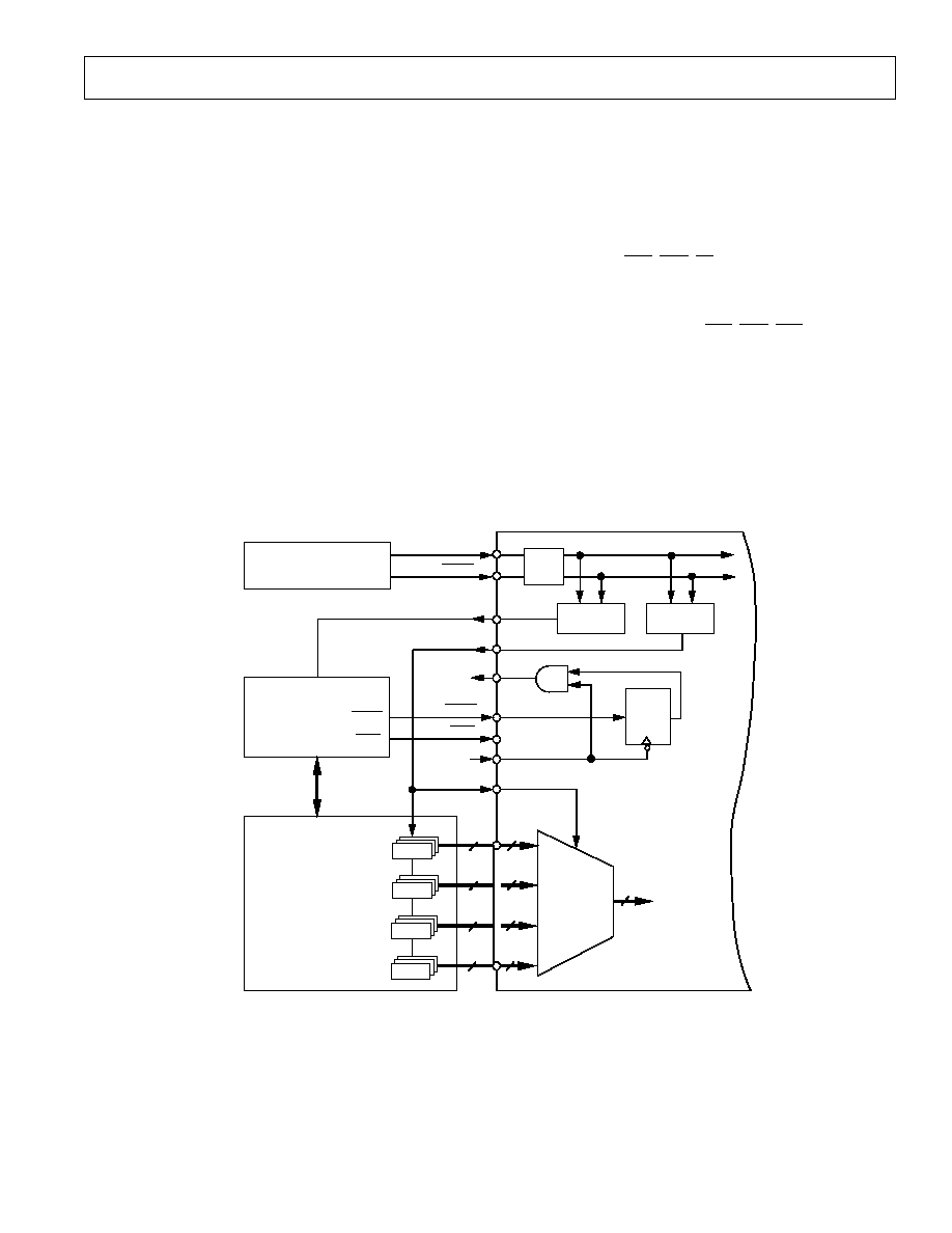
ADV7150
27
REV. A
Digital Signal Interconnect
The digital inputs to the ADV7150 should be isolated as much
as possible from the analog outputs and other analog circuitry.
Also, these input signals should not overlay the analog power
plane.
Due to the high clock rates involved, long clock lines to the
ADV7150 should be avoided to reduce noise pickup.
Any active termination resistors for the digital inputs should be
connected to the regular PCB power plane (V
CC
), and not the
analog power plane.
Analog Signal Interconnect
The ADV7150 should be located as close as possible to the out-
put connectors to minimize noise pick-up and reflections due to
impedance mismatch.
The video output signals should overlay the ground plane, and
not the analog power plane, to maximize the high frequency
power supply rejection.
Digital Inputs, especially Pixel Data Inputs and clocking signals
(CLOCK, LOADOUT, LOADIN, etc.) should never overlay
any of the analog signal circuitry and should be kept as far away
as possible.
For best performance, the analog outputs (IOR, IOG, IOB)
should each have a 75
load resistor connected to GND.
These resistors should be placed as close as possible to the
ADV7150 so as to minimize reflections. Normally, the differen-
tial analog outputs (IOR, IOG, IOB) are connected directly to
GND. In some applications, improvements in performance are
achieved by terminating these differential outputs with a resis-
tive load similar in value to the video load. For a doubly termi-
nated 75
load, this means that IOR, IOG, IOB are each
terminated with 37.5
resistors.
APPENDIX 2
TYPICAL FRAME BUFFER INTERFACE
CLOCK
ADV7150
CLOCK
LOADOUT
PRGCKOUT
LOADIN
SCKOUT
SCKIN
BLANK
LATCH
ENABLE
SYNC
ECL
TO
TTL
DIVIDE BY N
(
÷
N)
VRAM
(BANK A)
VRAM
(BANK B)
FRAME
BUFFER/
VIDEO
MEMORY
MULTIPLEXER
24
TO
PALETTE/RAM
& DAC
24
24
24
24
BLANK
SYNC
CLOCK
GRAPHICS
PROCESSOR/
CONTROLLER
VRAM
(BANK C)
24
24
VRAM
(BANK D)
24
24
33MHz
33MHz
33MHz
33MHz
DIVIDE BY M
(
÷
M)
CLOCK
GENERATOR
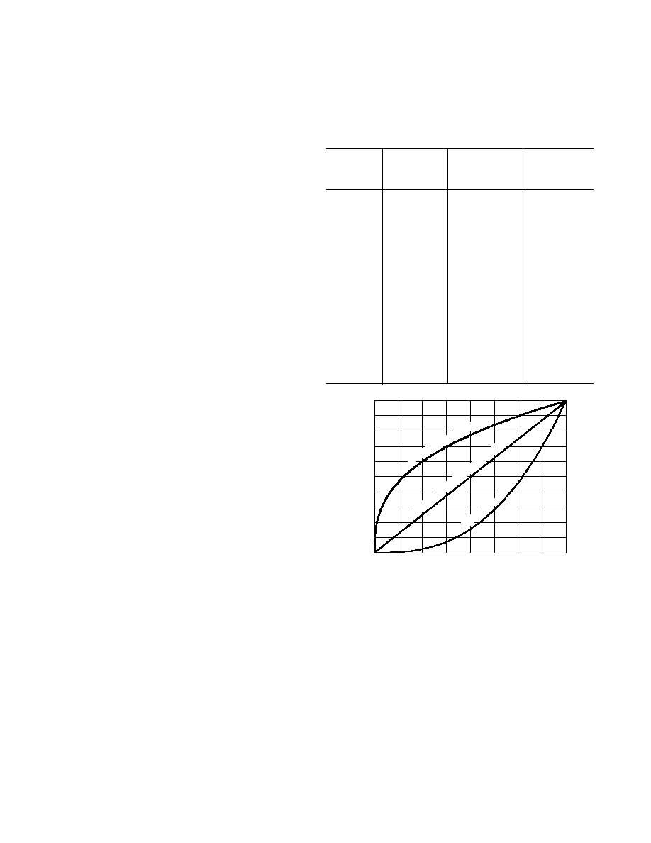
ADV7150
28
REV. A
10-Bit DACs
10-Bit RAM-DAC resolution allows for nonlinear video correc-
tion, in particular Gamma Correction. The ADV7150 allows for
an increase in color resolution from 24-bit to 30-bit effective
color without the necessity of a 30-bit deep frame buffer. In
true-color mode, for example, the part effectively operates as a
24-bit to 30-bit color look-up table.
Up to now we have assumed that there exists a linear relation-
ship between the actual RGB values input to a monitor and the
intensity produced on the screen. This, however, is not the case.
Half scale digital input (1000 0000) might correspond to only 20%
output intensity on the CRT (Cathode Ray Tube). The intensity
(I
CRT
) produced on a CRT by an input value I
IN
is given by:
I
CRT
= (I
IN
)
where
ranges from 2.0 to 2.8.
If the individual values of
for red, green and blue are known,
then so called "Gamma Correction" can be applied to each of
the three video input signals (I
IN
);
therefore:
I
IN(corrected)
= k(I
IN
)
1/
(k = 1, normally)
Traditionally, there has been a tradeoff between implementing a
nonlinear graphics function, such as gamma correction, and
color dynamic range. The ADV7150 overcomes this by increas-
ing the individual color resolution of each of the red, green and
blue primary colors from 8 bits per color channel to 10 bits per
channel (24 bits to 30 bits).
The table highlights the loss of resolution when 8-bit data is
gamma-corrected to a value of 2.7 and quantized in a tradi-
tional 8-bit system. Note that there is no change in the 8-bit
quantized data for linear changes in the input data over much of
the transfer function. On the other hand, when quantized to 10
bits via the 10-bit RAMs and 10-bit DACs of the ADV7150, all
changes on the input 8-bit data are reflected in corresponding
changes in the 10-bit data.
The graph shows a typical gamma curve corresponding to a
gamma value of 2.7. This is programmed to the red, green and
blue RAMs of the color lookup table instead of the more tradi-
tional linear function. Different curves corresponding to any
particular gamma value can be independently programmed to
each of the red, green and blue RAMs.
Other applications of the 10-bit RAM-DAC include closed-loop
monitor color calibration.
Gamma Correction 8 Bits vs. 10 Bits
Gamma
Corrected
Quantized to
Quantized to
8-Bit Data
(2.7)
8 Bits
10 Bits
240
0.977797
250
1001
241
0.979304
250
1002
242
0.980807
251
1004
243
0.982306
251
1005
244
0.983801
251
1007
245
0.985292
252
1008
246
0.986780
252
1010
247
0.988264
252
1011
248
0.989744
253
1013
249
0.991220
253
1015
250
0.992693
254
1016
251
0.994161
254
1018
252
0.995626
254
1019
253
0.997088
255
1021
254
0.998546
255
1022
255
1.000000
255
1023
1.00
0.00
256
0.30
0.10
32
0.20
0
0.60
0.40
0.50
0.70
0.80
0.90
224
192
160
128
96
64
INPUT CODE Decimal
DAC OUTPUT Normalized to 1
GAMMA CORRECTION CURVE
LINEAR RESPONSE PRECEIVED BY THE EYE
CRT RESPONSE
Gamma Correction Curve (Gamma Value = 2.7)
APPENDIX 3
10-BIT DACS AND GAMMA CORRECTION
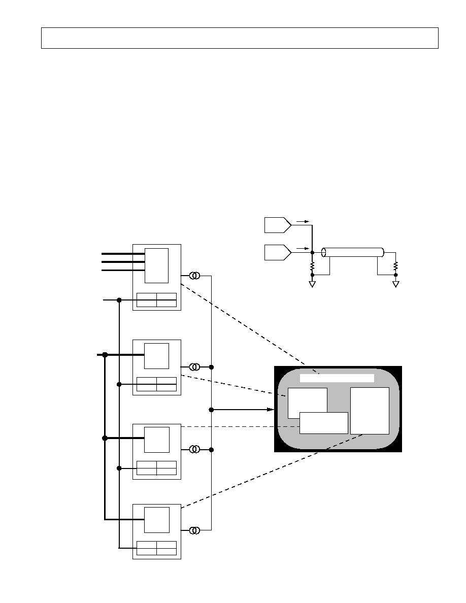
ADV7150
29
REV. A
APPENDIX 4
MULTIPLE PALETTE APPLICATIONS
Palette Priority Select Inputs
The palette priority selection inputs allow up to four separate
palette devices to be used in a single system to drive a single
monitor with subpixel resolution. The IOR, IOG and IOB ana-
log video output signals of each device are connected together,
as shown. Signal inputs (PS0, PS1) determine on a pixel by pixel
basis which palette device drives the monitor. This allows for
implementation of multiple windows applications with each
device acting as an independent palette. During initialization,
each device is assigned two match bits, MR16 (PS0) and MR17
(PS1) in Mode Register MR1. PS0 and PS1 inputs will select
one of the preprogrammed devices at any instant when PS0, PS1
matches MR16, MR17, respectively. PS0 and PS1 are multi-
plexed similar to the pixel data, thus allowing for subpixel resolu-
tion. The diagrams show an example of one ADV7150 operating in
conjunction with three ADV7151's (Pseudo-Color RAM-DACs).
Each displayed window on the monitor is driven by one of the
four devices, as determined on a pixel basis by PS0, PS1. Each
device's analog output signals are connected together as shown.
Note: Only one palette device is selected at any particular
instant. The analog output levels of the unselected devices will
be 0 mA.
Other applications for the palette priority function using a mini-
mum of two devices (one ADV7150 and one ADV7151) include:
Cursor Overlay on 24-Bit Graphics
Active Live Video Overlay (from Frame Grabber)
Text/Character Generation and Overlay
DACs
IOR,
IOG,
IOB
ZO = 75
ZS = 75
(SOURCE
TERMINATION)
ZL = 75
(MONITOR)
(CABLE)
DACs
IOR, IOG, IOB
(DEVICE: 2)
(DEVICE: 1)
Multiple Devices Termination for a Single Monitor
ADV7150
ADV7151 (1)
256 x 30
RAM
256 x 30
PALETTE
PALETTE SELECT BITS
ANALOG
O/P
RGB
ANALOG
VIDEO
VIDEO TO MONITOR
PS0, PS1
256 x 30
PALETTE
RGB
ANALOG
VIDEO
RGB
ANALOG
VIDEO
ADV7151 (2)
ADV7151 (3)
R0R7
G0G7
B0B7
WINDOW 1
(Pseudo-Color)
PS0=0: PS1=1
WINDOW 3
(Pseudo-Color)
PS0=1: PS1=1
MONITOR
WINDOW 2
(Pseudo-Color)
PS0=1: PS1=0
TRUE-COLOR BACKGROUND
MR16 MR17
0 0
PALETTE SELECT BITS
MR16 MR17
0 1
PALETTE SELECT BITS
MR16 MR17
1 0
PALETTE SELECT BITS
MR16 MR17
1 1
256 x 30
PALETTE
P0P7
Multiple Devices Driving a Multiwindow Application

ADV7150
30
REV. A
ADV7150 Initialization
After power has been supplied, the ADV7150 must be initial-
ized. The Mode Register and Control Registers must be set.
The values written to the various registers will be determined by
the desired operating mode of the part, i.e., True Color/Pseudo
Color, 2:1 Muxing/2:1 Muxing, etc.
The following section gives examples of initialization of the
ADV7150 operating in various modes.
Example 1
Color Mode
24-Bit True Color
Multiplexing
2:1
Databus
8-Bit
RAM-DAC Resolution
8-Bit
SYNC
Enabled on IOG
Pedestal
7.5 IRE
Register Initialization
C1
C0
R/W
Comment
Write
09H to Mode Register (MR1)
1
1
0
Resets to Normal Operation, 8-Bit Bus/RAM-DAC
Write
08H to Mode Register (MR1)
1
1
0
*(Initializes Pipelining
Write
09H to Mode Register (MR1)
1
1
0
*( "
Write
29H to Mode Register (MR1)
1
1
0
*(Calibrates LOADOUT/LOADIN Timing
Write
09H to Mode Register (MR1)
1
1
0
*( "
Write
04H to Address Register (A7A0)
0
0
0
Address Reg Points to Pixel Mask Register
Write
FFH to Pixel Mask Register
1
0
0
Sets the Pixel Mask to All "1s"
Write
05H to Address Register (A7A0)
0
0
0
Address Reg Points to Command Register 1 (CR1)
Write
00H to Command Reg 1 (CR1)
1
0
0
Write
06H to Address Register (A7A0)
0
0
0
Address Reg Points to Command Register 2 (CR2)
Write
ECH to Command Reg 2 (CR2)
1
0
0
Sets 24-Bit Color, 7.5 IRE, SYNC on Green (IOG)
Write
07H to Address Register (A7A0)
0
0
0
Address Reg Points to Command Register 3 (CR3)
Write
C0H to Command Reg 3 (CR3)
1
0
0
Sets 2:1 Multiplexing, PRGCKOUT = CLOCK/4
Color Palette RAM Initialization
C1
C0
R/W
Comment
Write
00H to Address Register (A7A0)
0
0
0
Points to Color Palette RAM
Write
00H (Red Data) to RAM Location (00H)
0
1
0
(Initializes Palette RAM
Write
00H (Green Data) to RAM Location (00H)
0
1
0
(
to a Linear Ramp**
Write
00H (Blue Data) to RAM Location (00H)
0
1
0
(
Write
01H (Red Data) to RAM Location (01H)
0
1
0
(
Write
01H (Green Data) to RAM Location (01H)
0
1
0
(
Write
01H (Blue Data) to RAM Location (01H)
0
1
0
(
·
·
·
·
·
·
·
·
(
·
·
·
·
·
·
·
·
(
Write
FFH (Red Data) to RAM Location (FFH)
0
1
0
(
Write
FFH (Green Data) to RAM Location (FFH)
0
1
0
(
Write
FFH (Blue Data) to RAM Location (FFH)
0
1
0
(RAM Initialization Complete
*
*These four command lines reset the ADV7150. The pipelines for each of the Red, Creen and Blue pixel inputs are synchronously reset to the Multiplexer's
"A" input. Mode Register bit MR10 is written by a "1" followed by "0" followed by "1." LOADIN/LOADOUT timing is internally synchronized by writing a "0"
followed by a "1" followed by a "0" to Mode Register MR15.
**This sequence of instructions would, of course, normally be coded using some form of loop instruction.
APPENDIX 5
INITIALIZATION AND PROGRAMMING

ADV7150
31
REV. A
Example 2
Color Mode
24-Bit Gamma Corrected True Color (30 Bits)
Multiplexing
2:1
Databus
10 Bit
RAM-DAC Resolution
10 Bit
SYNC
Ignored
Pedestal
0 IRE
Calibration
Every Vertical Sync
Register Initialization
C1
C0
R/W
Comment
Write
0FH to Mode Register (MR1)
1
1
0
Resets to Normal Operation, 10-Bit Bus/RAM-DAC
Write
0EH to Mode Register (MR1)
1
1
0
*(Initializes Pipelining
Write
0FH to Mode Register (MR1)
1
1
0
*(
"
Write
2FH to Mode Register (MR1)
1
1
0
*(Calibrates LOADOUT/LOADIN Timing
Write
0FH to Mode Register (MR1)
1
1
0
*(
"
Write
04H to Address Register (A7A0)
0
0
0
Address Reg Points to Pixel Mask Register
Write
FFH to Pixel Mask Register
1
0
0
Sets the Pixel Mask to All "1s"
Write
05H to Address Register (A7A0)
0
0
0
Address Reg Points to Command Register 1 (CR1)
Write
01H to Command Reg 1 (CR1)
0
0
0
Calibrates Every Vertical Sync
Write
06H to Address Register (A7A0)
0
0
0
Address Reg Points to Command Register 2 (CR2)
Write
E0H to Command Reg 2 (CR2)
1
0
0
Sets 24-Bit Color, 0 IRE, No SYNC
Write
07H to Address Register (A7A0)
0
0
0
Address Reg Points to Command Register 3 (CR3)
Write
41H to Command Reg 3 (CR3)
1
0
0
Sets 2:1 Multiplexing, PRGCKOUT = CLOCK/8
Color Palette RAM Initialization
C1
C0
R/W
Comment
Write
00H to Address Register (A7A0)
0
0
0
Points to Color Palette RAM
Write
000H (Red Data) to RAM Location (00H)
0
1
0
(Initializes Palette RAM
Write
000H (Green Data) to RAM Location (00H)
0
1
0
(
to a "Gamma" Ramp**
Write
000H (Blue Data) to RAM Location (00H)
0
1
0
(
Write
xxxH (Red Data) to RAM Location (01H)
0
1
0
(
Write
xxxH (Green Data) to RAM Location (01H)
0
1
0
(
Write
xxxH (Blue Data) to RAM Location (01H)
0
1
0
(
·
·
·
·
·
·
·
·
(
·
·
·
·
·
·
·
·
(
Write
3FFH (Red Data) to RAM Location (FFH)
0
1
0
(
Write
3FFH (Green Data) to RAM Location (FFH)
0
1
0
(
Write
3FFH (Blue Data) to RAM Location (FFH)
0
1
0
(RAM Initialization Complete
*
*These four command lines reset the ADV7150 The pipelines for each of the Red, Green and Blue pixel inputs are synchronously reset to the Multiplexer's "A" in-
put. Mode Register bit MR10 is written by a "1" followed by "0" followed by "1." LOADIN/LOADOUT timing is internally synchronized by writing a "0" followed
by a "1" followed by a "0" to Mode Register MR15.
**Data for a gamma curve characteristic is obtainable in Appendix 3.
REGISTER DIAGNOSTIC TESTING
The previous examples show the register initialization sequence
for the ADV7150. These show control data going to the regis-
ters and palette RAM. As well as this writing function, it may
also be necessary, due to system diagnostic requirements, to
confirm that correct data has been transferred to each register
and palette RAM location. There are two ways to incorporate
register value/RAM value checking:
1. READ after each WRITE: After data is written to a particular
register, it can be read back immediately. The following table
shows an example with Command Registers CR2 and CR3.
C1 C0
R/W
D0D7
Comment
0
0
0
06H
Select Command Register 2 (CR2)
1
0
0
E0H
Sets 24-Bit True-Color
1
0
1
E0H
Command Reg 2 Value Read-Back
0
0
0
07H
Select Command Register 3 (CR3)
1
0
0
40H
Set 2:1 Mux Mode
1
0
1
40H
Command Reg 3 Value Read-Back
2. READ after all WRITEs completed: All registers and the
color palette RAM are written to and set. Once this is
complete, all registers are again accessed but this time in
Read-Only mode. The table below shows this method for
Command Registers CR2 and CR3.
C1
C0
R/W
D0D7
Comment
0
0
0
06H
Select Command Register 2 (CR2)
1
0
0
E0H
Sets 24-Bit True-Color
0
0
0
07H
Select Command Register 3 (CR3)
1
0
0
40H
Set 2:1 Mux Mode
0
0
0
06H
Select CR2
1
0
1
E0H
CR2 Value Read-Back
0
0
0
07H
Select CR3
1
0
1
40H
CR3 Value Read-Back
1
0
1
40H
CR3 Value Read-Back
It is clear that this latter case requires more command lines
than the previous READ after each WRITE case.
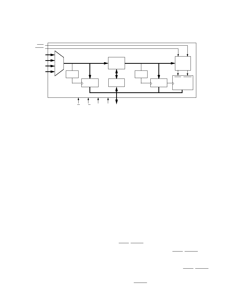
ADV7150
32
REV. A
the graphics pipeline and after a number of clocks get latched
into the DAC Test Register. This data can then be read from
the Pixel Test Register and the DAC Test Registers over the
MPU Port. This data will remain in the Pixel Test Registers and
the DAC Test Registers until the next rising edge of R7 causes
new data to be latched in.
In the above example, the next rising edge of R7 occurs on the
Pixel n input. Therefore the data in the Pixel Test Registers and
DAC Test Registers must be read over the MPU before the
Pixel n data is applied, otherwise they will be overwritten by the
Pixel n data and the Pixel 2 data will be lost.
Pixel Test Register
The read-only Pixel Test Register is 24 bits wide, 8 bits each for
red green and blue. It is situated directly after the Pixel Mask
Register. After data is latched into this register by a transition on
R7, it is read in three cycles over the MPU Port as described in
the "Microprocessor (MPU) Port" section.
DAC Test Register
The DAC Test Register is latched with data some CLOCKs
after the Pixel Test Register. The DAC Test Register is a 30-bit
wide read-only register, corresponding to 10 bits each for red,
green and blue data. It is located the Color Palette RAM. If the
RAM-DAC is in 8-bit after resolution mode, the upper two bits
of the red, green and blue data will be zero. After data is latched
into the DAC Test Register by a transition on R7, it is read
in three or six cycles over the MPU Port as described in the
"Microprocessor (MPU) Port" section.
SYNC
, BLANK and I
PLL
Test Register
This is an 8-bit wide register but with only three effective bits.
The three lower bits correspond to SYNC, BLANK and I
PLL
respectively. The upper bits should be masked in software. This
register is at the same position in the graphics pipeline as the
DAC Test Register. When pixel data is latched into the DAC
Test Register, the corresponding status of SYNC, BLANK and
I
PLL
is latched into this register. It is read over the MPU Port as
described in the "Microprocessor (MPU) Port" section.
(Note: If BLANK is low, the corresponding pixel data to the
DAC Test Register will be all "0s.")
The ADV7150 contains onboard circuitry which enables both
device and system level test diagnostics. The test circuitry can
be used to test the frame buffer memory as well as the function-
ality of the ADV7150. A number of test registers are integrated
into the part which effectively allow for monitoring of the graph-
ics pipeline. Pixel data is read from the graphics pipeline inde-
pendent of the pixel CLOCK. The pixel data itself contains the
triggering information that latches data into the test registers.
This allows for system diagnostics in a continuously clocked
graphics system. The test register data is then read by the micro-
processor over the MPU.
Access to the test registers is as described in the "Microproces-
sor (MPU) Port" section. This section also gives the address
decode locations for the various test registers.
Test Trigger (R7)
The test trigger is decoded from the pixel data stream. Bit R7 of
the RED channel is assigned the task of latching pixel data into
the test registers. A "0" to "1" or a "1" to "0" (as determined
by bit CR20 of Command Register 2) transition on R7, fills the
test register with the corresponding pixel data. This effectively
means that a sequence of data travels along the graphics pipe-
line, with the test registers taking a sample only when there is a
transition on Bit R7. The following example shows a sequence
with the ADV7150 preset to sample the graphics pipeline on a
low to high transition of R7.
RED
GREEN
BLUE
Pixel 0:
00000000
00000000
00000000
Pixel 1:
0........
........
........
Pixel 2:
1........
........
........
Pixel 3:
0........
........
........
. . . .
. . .
. . . .
. . .
Pixel n- l:
0........
........
........
Pixel n:
1........
........
........
Pixel n:
0........
........
........
In the above sequence of pixels, there is a rising edge on R7 on
Pixel 2. The Red, Green and Blue data for Pixel 2, therefore,
gets latched into the Pixel Test Register. Pixel 2 continues down
APPENDIX 6
TEST DIAGNOSTICS
MPU PORT
CE
R/W
C0
C1
D0D9
PIXEL TEST
REGISTER
DAC TEST
REGISTERS
COLOR
REGISTERS
COLOR
PALETTE
RAM
TRIGGER
DECODE
TRIGGER
DECODE
GRAPHICS PIPELINE
GRAPHICS PIPELINE
INPUT
MUX
PIXEL
DATA
SYNC
BLANK
DACs
SYNC
BLANK
I
PLL
REGISTER
TEST
Test/Diagnostic Block Diagram
ADV7150
33
REV. A
APPENDIX 7
THERMAL AND ENVIRONMENTAL CONSIDERATIONS
The ADV7150 is a very highly integrated monolithic silicon
device. This high level of integration, in such a small package,
inevitably leads to consideration of thermal and environmental
conditions in which the ADV7150 must operate. Reliability of
the device is significantly enhanced by keeping it as cool as pos-
sible. In order to avoid destructive damage to the device, the
absolute maximum junction temperature of 150
°
C must never
be exceeded. Certain applications, depending on pixel data
rates, may require forced air cooling, or external heatsinks. The
following data is intended as a guide in evaluating the operating
conditions of a particular application so that optimum device
and system performance is achieved.
It should be noted that information on package characteristics pub-
lished herein may not be the most up to date at the time of reading
this. Advances in package compounds and manufacture will inevita-
bly lead to improvements in the thermal data. Please contact your
local sales office for the most up-to-date information.
Power Dissipation
The diagram shows graphs of power dissipation in watts vs.
pixel clock frequency for the ADV7150.
POWER DISSIPATION W
atts
1.50
0.50
1.25
0.75
1.00
PIXEL CLOCK FREQUENCY MHz
60
220
80
180
200
160
140
120
100
V
AA
= 5V
V
REF
= 1.2V
T
A
= +25
°
C
NOTE: THE "WORST CASE ON-SCREEN PATTERN" CORRESPONDS TO FULL-SCALE
TRANSITION ON EACH PIXEL VALUE FOR EVERY CLOCK EDGE (00H, FFH, 00H, ... ).
THE "TYPICAL ON-SCREEN PATTERN" CORRESPONDS TO LINEAR CHANGES IN THE
PIXEL INPUT (I. E., A BLACK TO WHITE RAMP). IN GENERAL, COLOR IMAGES TEND
TO APPROXIMATE THIS CHARACTERISTIC.
Typical Power Dissipation vs. Pixel Rate
Package Characteristics
The table of thermal characteristics shows typical information
for the ADV7150 (160-Lead Plastic Power QFP) using various
values of Airflow.
Junction to Case (
JC
) Thermal Resistance for this particular
part is:
JC
(160-Lead Plastic Power QFP) = 1.0
°
C/W
(Note:
JC
is independent of airflow.)
Table A. Thermal Characteristics vs. Airflow
Air Velocity
0
50
100
200
(Linear feet/min)
(Still Air)
JA
(
°
C/W)
No Heatsink
25.5
23
21
19
EG&G D10100-28 Heatsink 23
20
18
16
Thermalloy 2290 Heatsink
19
17
15
12
Thermal Model
The junction temperature of the device in a specific application
is given by:
T
J
= T
A
+ P
D
(
JC
+
CA
)
(1)
or
T
J
= T
A
+ P
D
(
JA
)
(2)
where:
T
J
= Junction Temperature of Silicon (
°
C)
T
A
= Ambient Temperature (
°
C)
P
D
= Power Dissipation (W)
JC
= Junction to Case Thermal Resistance (
°
C/W)
CA
= Case to Ambient Thermal Resistance (
°
C/W)
JA
= Junction to Ambient Thermal Resistance (
°
C/W)
Package Enhancements
The standard QFP package has been enhanced to a PowerQuad2
package. This supports an improved thermal performance com-
pared to standard QFP. In this case, the die is attached to
heatslug so that the power that is dissipated can be conducted to
the external surface of the package. This provides a highly effi-
cient path for the transfer of heat to the package surface. The
package configuration also provides an efficient thermal path
from the ADV7150 to the Printed Circuit Board via the leads.
Heatsinks
The maximum silicon junction temperature should be limited to
100
°
C. Temperatures greater than this will reduce long term
device reliability. To ensure that the silicon junction tempera-
ture stays within prescribed limits, the addition of an external
heatsink may be necessary. Heatsinks, will reduce
JA
as shown
in the "Thermal Characteristics vs. Airflow" table.
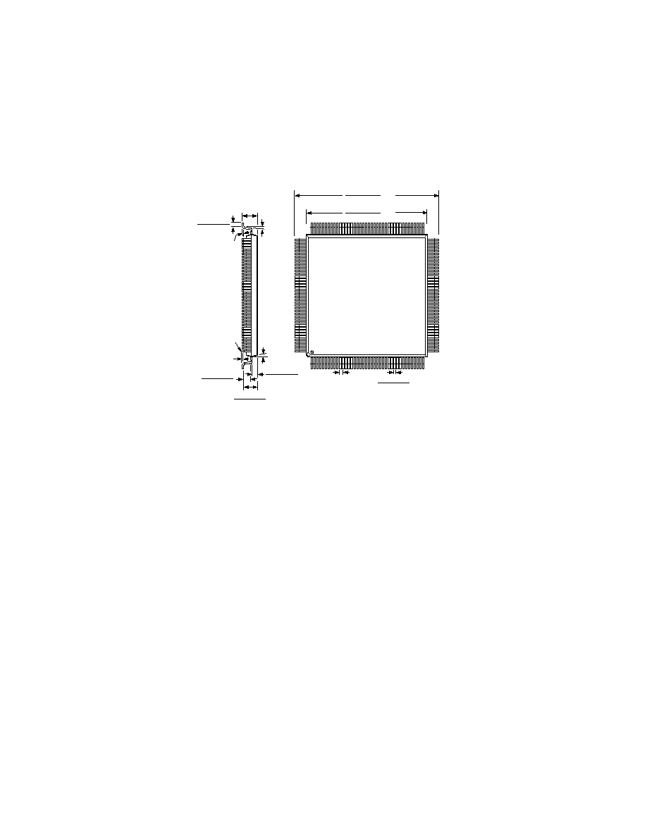
ADV7150
34
REV. A
APPENDIX 8
OUTLINE DIMENSIONS
Dimensions shown in inches and (mm).
S-160
160-Lead Plastic Power Quad Flatpack
TOP VIEW
(PINS DOWN)
PIN 1
121
160
1
120
41
40
80
81
0.014 (0.35)
0.011 (0.27)
1.239 (31.45)
1.219 (30.95)
1.107 (28.10)
1.100 (27.90)
SQ
SQ
0.026 (0.65) MIN
SEATING
PLANE
0.160 (4.07)
MAX
0.037 (0.95)
0.026 (0.65)
0.004 (0.10)
MAX
0.145 (3.67)
0.125 (3.17)
0.070 (1.77)
0.062 (1.57)
0.070 (1.77)
0.062 (1.57)
10
°
6
°±
4
°
4
°±
4
°
MAX

35

C1695108/94
PRINTED IN U.S.A.
36
REV. A