Äîêóìåíòàöèÿ è îïèñàíèÿ www.docs.chipfind.ru
REV. B
Information furnished by Analog Devices is believed to be accurate and
reliable. However, no responsibility is assumed by Analog Devices for its
use, nor for any infringements of patents or other rights of third parties
which may result from its use. No license is granted by implication or
otherwise under any patent or patent rights of Analog Devices.
a
CMOS 220 MHz True-Color Graphics
Triple 10-Bit Video RAM-DAC
ADV7152
One Technology Way, P.O. Box 9106, Norwood, MA 02062-9106, U.S.A.
Tel: 617/329-4700
Fax: 617/326-8703
FEATURES
220 MHz, 24-Bit (30-Bit Gamma Corrected) True Color
Triple 10-Bit "Gamma Correcting" D/A Converters
Triple 256 10 (256 30) Color Palette RAM
On-Chip Clock Control Circuit
Palette Priority Select Registers
RS-343A/RS-170 Compatible Analog Outputs
TTL Compatible Digital Inputs
Standard MPU l/O Interface
10-Bit Parallel Structure
8+2 Byte Structure
Programmable Pixel Port: 24-Bit and 8-Bit (Pseudo)
Pixel Data Serializer
Multiplexed Pixel Input Ports; 1:1, 2:1
+5 V CMOS Monolithic Construction
100-Lead Plastic Quad Flatpack (QFP)
Thermally Enhanced to Achieve
JC
< 1.0 C/W
MODES OF OPERATION
24-Bit True Color (30-Bit Gamma Corrected)
@ 220 MHz
@ 170 MHz
@ 135 MHz
@ 110 MHz
@ 85 MHz
8-Bit Pseudo Color
15-Bit True Color
APPLICATIONS
High Resolution, True Color Graphics
Professional Color Prepress Imaging
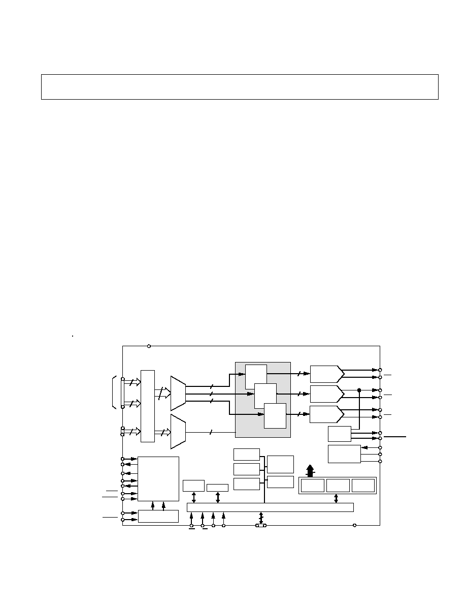
GENERAL DESCRIPTION
The ADV7152 (ADV
®
) is a complete analog output, Video
RAM-DAC on a single CMOS monolithic chip. The part is spe-
cifically designed for use in high performance, color graphics
workstations. The ADV7152 integrates a number of graphic
functions onto one device allowing 24-bit direct True-Color op-
eration at the maximum screen update rate of 220 MHz. The
ADV7152 implements 30-bit True Color in 24-bit frame buffer
designs. The part also supports other modes, including 15-bit
True Color and 8-bit Pseudo or Indexed Color. Either the Red,
Green or Blue input pixel ports can be used for Pseudo Color.
The device consists of three, high speed, 10-bit, video D/A con-
verters (RGB), three 256 10 (one 256 30) color look-up
tables, palette priority selects, a pixel input data multiplexer/
serializer and a clock generator/divider circuit. The ADV7152
implements 1:1 and 2:1 pixel data multiplexing. The onboard
palette priority select inputs enable multiple palette devices to
be connected together for use in multipalette and window
(Continued on page 10)
ADV is a registered trademark of Analog Devices, Inc.
FUNCTIONAL BLOCK DIAGRAM
256-COLOR/GAMMA
PALETTE RAM
10
IOR
48
A
B
24
24
P
I
X
E
L
P
O
R
T
MUX
2:1
30
RED
256 x 10
MPU PORT
D9 D0
10 (8+2)
C0
C1
LOADIN
CLOCK
LOADOUT
PRGCKOUT
SCKIN
SCKOUT
CLOCK DIVIDE
&
SYNCHRONIZATION
CIRCUIT
÷
32,
÷
16,
÷
8,
÷
4,
÷
2
ADDR
(A0-A15)
REVISION
REGISTER
COMMAND
REGISTERS
(CR1-CR3)
TEST
REGISTERS
(MR1)
VOLTAGE
REFERENCE
CIRCUIT
ADV7152
V
REF
R
SET
C
OMP
SYNC
OUTPUT
I
PLL
RED (R0R7),
GREEN (G0G7),
BLUE (B0B7)
COLOR DATA
V
AA
GND
DATA TO
PALETTES
CONTROL REGISTERS
COLOR REGISTERS
ADDRESS
REGISTER
CLOCK CONTROL
MODE
REGISTER
GREEN
256 x 10
BLUE
256 x 10
PALETTE
SELECTS
(PS0, PS1)
ID
REGISTER
PIXEL MASK
REGISTER
8
CE R/W
IOR
IOG
IOG
IOB
IOB
10-BIT
GREEN DAC
10
10
BLUE
REGISTER
RED
REGISTER
ECL TO CMOS
8
8
2
4
4
SYNC
BLANK
CLOCK
MUX
2:1
10-BIT
RED DAC
10-BIT
BLUE DAC
GREEN
REGISTER
SYNCOUT
REV. B
2
ADV7152SPECIFICATIONS
(V
AA
1
= +5 V; V
REF
= +1.235 V; R
SET
= 280
. IOR, IOG, IOB (R
L
= 37.5
,
C
L
= 10 pF); IOR, IOG, IOB = GND. All specifications T
MIN
to T
MAX
2
unless otherwise noted.)
Parameter
All Versions
Unit
Test Conditions/Comments
STATIC PERFORMANCE
Resolution (Each DAC)
10
Bits
Accuracy (Each DAC)
Integral Nonlinearity
±
1
LSB max
Differential Nonlinearity
±
1
LSB max
Guaranteed Monotonic
Gray Scale Error
±
5
% Gray Scale max
Coding
Binary
DIGITAL INPUTS (Excluding CLOCK, CLOCK)
Input High Voltage, V
INH
2
V min
Input Low Voltage, V
INL
0.8
V max
Input Current, I
IN
±
10
µ
A max
V
IN
= 0.4 V or 2.4 V
Input Capacitance, C
IN
10
pF typ
CLOCK INPUTS (CLOCK, CLOCK)
Input High Voltage, V
INH
V
AA
1.0
V min
Input Low Voltage, V
INL
V
AA
1.6
V max
Input Current, I
IN
±
10
µ
A max
V
IN
= 0.4 V or 2.4 V
Input Capacitance, C
IN
10
pF typ
DIGITAL OUTPUTS
Output High Voltage, V
OH
2.4
V min
I
SOURCE
= 400
µ
A
Output Low Voltage, V
OL
0.4
V max
I
SINK
= 3.2 mA
Floating-State Leakage Current
20
µ
A max
Floating-State Output Capacitance
20
pF typ
ANALOG OUTPUTS
Gray Scale Current Range
15/22
mA min/max
Output Current
White Level Relative to Blank
17.69/20.40
mA min/max
Typically 19.05 mA
White Level Relative to Black
16.74/18.50
mA min/max
Typically 17.62 mA
Black Level Relative to Blank
0.95/1.90
mA min/max
Typically 1.44 mA
Blank Level on IOR, IOB
0/50
µ
A min
Typically 5
µ
A
Blank Level on IOG
6.29/8.96
mA min/max
Typically 7.62 mA
Sync Level on IOG
0/50
µ
A min/max
Typically 5
µ
A
LSB Size
17.22
µ
A typ
DAC-to-DAC Matching
3
% max
Typically 1%
Output Compliance, V
OC
0/+1.4
V min/V max
Output Impedance, R
OUT
100
k
typ
Output Capacitance, C
OUT
30
pF max
I
OUT
= 0 mA
VOLTAGE REFERENCE
Voltage Reference Range, V
REF
1.14/1.26
V min/V max
V
REF
= 1.235 V for Specified Performance
Input Current, I
VREF
+5
µ
A typ
POWER REQUIREMENTS
V
AA
5
V nom
I
AA
3
400
mA max
220 MHz Parts
I
AA
370
mA max
170 MHz Parts
I
AA
350
mA max
135 MHz Parts
I
AA
330
mA max
110 MHz Parts
I
AA
315
mA max
85 MHz Parts
Power Supply Rejection Ratio
0.5
%/% max
Typically 0.12%/%, COMP = 0.1
µ
F
DYNAMIC PERFORMANCE
Clock and Data Feedthrough
4, 5
30
dB typ
Glitch Impulse
50
pV secs typ
DAC-to-DAC Crosstalk
6
23
dB typ
NOTES
1
±
5% for all versions.
2
Temperature range (T
MIN
to T
MAX
): 0
°
C to +70
°
C; T
J
(Silicon Junction Temperature)
100
°
C.
3
Pixel Port is continuously clocked with data corresponding to a linear ramp. T
J
= 100
°
C.
4
Clock and data feedthrough is a function of the amount of overshoot and undershoot on the digital inputs. Glitch impulse includes clock and data feedthrough.
5
TTL input values are 0 to 3 volts, with input rise/fall times
3 ns, measured the 10% and 90% points. Timing reference points at 50% for inputs and outputs.
6
DAC-to-DAC crosstalk is measured by holding one DAC high while the other two are making low-to-high and high-to-low transitions.
Specifications subject to change without notice.
ADV7152
3
REV. B
TIMING CHARACTERISTICS
1
CLOCK CONTROL AND PIXEL PORT
4
220 MHz
170 MHz
135 MHz
110 MHz
85 MHz
Parameter
Version
Version
Version
Version
Version
Units
Conditions/Comments
f
CLOCK
220
170
135
110
85
MHz max Pixel CLOCK Rate
t
1
4.55
5.88
7.4
9.1
11.77
ns min
Pixel CLOCK Cycle Time
t
2
2
2.5
3
4
4
ns min
Pixel CLOCK High Time
t
3
2
2.5
3.2
4
4
ns min
Pixel CLOCK Low Time
t
4
10
10
10
10
10
ns max
Pixel CLOCK to LOADOUT Delay
f
LOADIN
LOADIN Clocking Rate
1:1 Multiplexing
110
110
110
110
85
MHz max
2:1 Multiplexing
110
85
67.5
55
42.5
MHz max
t
5
LOADIN Cycle Time
1:1 Multiplexing
9.1
9.1
9.1
9.1
11.76
ns min
2:1 Multiplexing
9.1
11.76
14.8
18.18
23.53
ns min
t
6
LOADIN High Time
1:1 Multiplexing
4
4
4
4
4
ns min
2:1 Multiplexing
4
5
6
8
9
ns min
t
7
LOADIN Low Time
1:1 Multiplexing
4
4
4
4
4
ns min
2:1 Multiplexing
4
5
6
8
9
ns min
t
8
0
0
0
0
0
ns min
Pixel Data Setup Time
t
9
5
5
5
5
5
ns min
Pixel Data Hold Time
t
10
0
0
0
0
0
ns min
LOADOUT to LOADIN Delay
t
11
5
5
5
5
5
5
ns max
LOADOUT to LOADIN Delay
t
PD
6
Pipeline Delay
1:1 Multiplexing
5
5
5
5
5
CLOCKs
(1
×
CLOCK = t
1
)
2:1 Multiplexing
6
6
6
6
6
CLOCKs
t
12
10
10
10
10
10
ns max
Pixel CLOCK to PRGCKOUT Delay
t
13
5
5
5
5
5
ns max
SCKIN to SCKOUT Delay
t
14
5
5
5
5
5
ns min
BLANK
to SCKIN Setup Time
t
15
1
1
1
1
1
ns min
BLANK
to SCKIN Hold Time
ANALOG OUTPUTS
7
220 MHz 170 MHz 135 MHz 110 MHz 85 MHz
Parameter
Version
Version
Version
Version
Version
Units
Conditions/Comments
t
16
15
15
15
15
15
ns typ
Analog Output Delay
t
17
1
1
1
1
1
ns typ
Analog Output Rise/Fall Time
t
18
15
15
15
15
15
ns typ
Analog Output Transition Time
t
SK
2
2
2
2
2
ns max
Analog Output Skew (IOR, IOG, IOB)
0
0
0
0
0
ns typ
MPU PORTS
8, 9
220 MHz 170 MHz 135 MHz 110 MHz 85 MHz
Parameter
Version
Version
Version
Version
Version
Units
Conditions/Comments
t
19
3
3
3
3
3
ns min
R/W, C0, C1 to CE Setup Time
t
20
10
10
10
10
10
ns min
R/W, C0, C1 to CE Hold Time
t
21
45
45
45
45
45
ns min
CE
Low Time
t
22
25
25
25
25
25
ns min
CE
High Time
t
23
8
5
5
5
5
5
ns min
CE
Asserted to Databus Driven
t
24
9
45
45
45
45
45
ns max
CE
Asserted to Data Valid
t
25
9
20
20
20
20
20
ns max
CE
Disabled to Databus Three-Stated
5
5
5
5
5
ns min
t
26
20
20
20
20
20
ns min
Write Data (D0D9) Setup Time
t
27
5
5
5
5
5
ns min
Write Data (D0D9) Hold Time
(V
AA
2
= +5 V; V
REF
= +1.235 V; R
SET
= 280
. IOR, IOG, IOB (R
L
= 37.5 , C
L
= 10 pF);
IOR
, IOG, I0B = GND. All specifications T
MIN
to T
MAX
3
unless otherwise noted.)
ADV7152
4
REV. B
NOTES
1
TTL input values are 0 to 3 volts, with input rise/fall times
3 ns, measured between the 10% and 90% points. ECL inputs (CLOCK, CLOCK) are
V
AA
0.8 V to V
AA
1.8 V, with input rise/fall times
2 ns, measured between the 10% and 90% points. Timing reference points at 50% for inputs and out-
puts. Analog output load
10 pF. Databus (D0D9) loaded as shown in Figure 1. Digital output load for LOADOUT, PRGCKOUT, SCKOUT, I
PLL
and
SYNCOUT
30 pF.
2
±
5% for all versions.
3
Temperature range (T
MIN
to T
MAX
): 0
°
C to +70
°
C; T
J
(Silicon Junction Temperature)
100
°
C.
4
Pixel Port consists of the following inputs: Pixel Inputs: RED [A, B]; GREEN [A, B]; BLUE [A, B], Palette Selects: PS0 [A, B]; PS1 [A, B]; Pixel Controls:
SYNC
, BLANK; Clock Inputs: CLOCK, CLOCK, LOADIN, SCKIN; Clock Outputs: LOADOUT, PRGCKOUT, SCKOUT.
5
is the LOADOUT Cycle Time and is a function of the Pixel CLOCK Rate and the Multiplexing Mode: 1:1 multiplexing;
= CLOCK = t
1
ns; 2:1 multi-
plexing,
= CLOCK
×
2 = 2
×
t
1
ns.
6
These fixed values for Pipeline Delay are valid under conditions where t
10
and
t
11
are met. If either t
10
or
t
11
are not met, the part will operate but the Pipe-
line Delay is increased by 2 clock cycles for 2:1 mode after calibration cycle is performed.
7
Output delay measured from the 50% point of the rising edge of CLOCK to the 50% point of full-scale transition. Output rise/fall time measured between the
10% and 90% points of full-scale transition. Settling time measured from the 50% point of full-scale transition to the output remaining within
±
1 LSB. (Settling time
does not include clock and data feedthrough.)
8
t
23
and t
24
are measured with the load circuit of Figure 1 and defined as the time required for an output to cross 0.4 V or 2.4 V.
9
t
25
is derived from the measured time taken by the data outputs to change by 0.5 V when loaded with the circuit of Figure 1. The measured number is then extrapo-
lated back to remove the effects of charging the 100 pF capacitor. This means that the time, t
25
, quoted in the Timing Characteristics is the true value for the device
and as such is independent of external databus loading capacitances.
Specifications subject to change without notice.
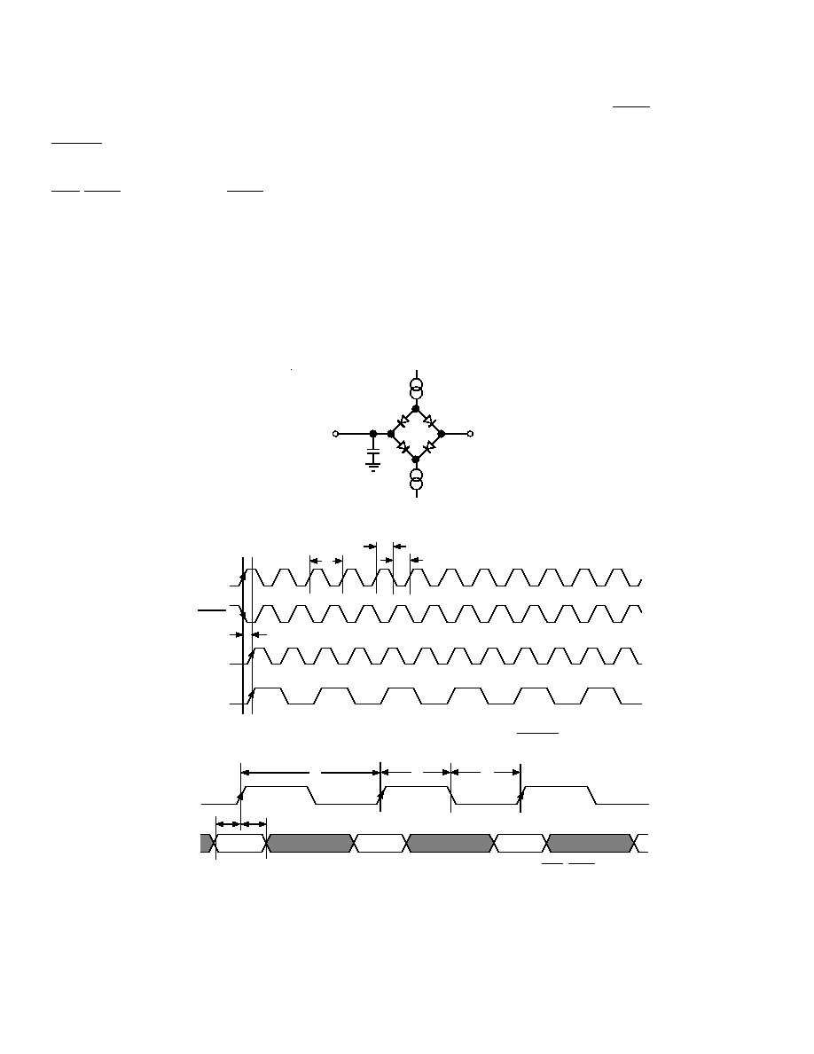
I
SINK
+2.1V
TO
OUTPUT
PIN
I
SOURCE
100pF
Figure 1. Load Circuit for Databus Access and Relinquish Times
t
3
t
2
CLOCK
LOADOUT
(1:1 MULTIPLEXING)
LOADOUT
(2:1 MULTIPLEXING)
CLOCK
t
4
t
1
Figure 2. LOADOUT vs. Pixel Clock Input (CLOCK, CLOCK)
PIXEL INPUT
DATA*
LOADIN
t
8
t
9
*INCLUDES PIXEL DATA (R0-R7, G0-G7, B0-B7); PALETTE SELECT INPUTS (PS0-PS1); SYNC; BLANK
VALID
DATA
VALID
DATA
VALID
DATA
t
5
t
6
t
7
Figure 3. LOADIN vs. Pixel Input Data
ADV7152
5
REV. B
PIXEL INPUT
DATA*
CLOCK
LOADOUT
LOADIN
ANALOG
OUTPUT
DATA
t
10
A
N
B
N
A
N+1
B
N+1
A
N-1
B
N-1
A
N+2
B
N+2
A
N
B
N
A
N+1
B
N+1
A
N+2
B
N+2
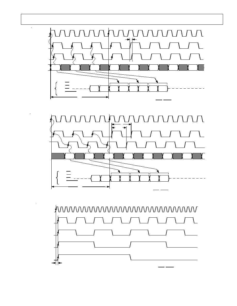
DIGITAL INPUT TO ANALOG OUTPUT PIPELINE
t
PD
*INCLUDES PIXEL DATA (R0R7, G0G7, B0B7); PALETTE SELECT INPUTS (PS0-PS1); SYNC; BLANK
IOR, IOR
IOG, IOG
IOB, IOB
I
PLL
, SYNCOUT
Figure 4. Pixel Input to Analog Output Pipeline with Minimum LOADOUT to LOADIN Delay (2:1 Multiplex Mode)
PIXEL INPUT
DATA*
CLOCK
LOADOUT
LOADIN
ANALOG
OUTPUT
DATA
*INCLUDES PIXEL DATA (R0R7, G0G7, B0B7); PALETTE SELECT INPUTS (PS0PS1); SYNC; BLANK
DIGITAL INPUT TO ANALOG OUTPUT PIPELINE
A
N
B
N
A
N+1
B
N+1
A
N+2
B
N+2
A
N
B
N
A
N+1
B
N+1
A
N-1
B
N-1
A
N+2
B
N+2
t
PD
- t
11
IOR, IOR
IOG, IOG
IOB, IOB
I
PLL
, SYNCOUT
Figure 5. Pixel Input to Analog Output Pipeline with Maximum LOADOUT to LOADIN Delay (2:1 Multiplex Mode)
t
12
CLOCK
PRGCKOUT
(CLOCK/4)
PRGCKOUT
(CLOCK/8)
PRGCKOUT
(CLOCK/16)
PRGCKOUT
(CLOCK/32)
*INLCUDES PIXEL DATA (R0-R7, G0-G7, B0-B7); PALETTE SELECT INPUTS (PS0-PS1); SYNC; BLANK
Figure 6. Pixel Clock Input vs. Programmable Clock Output (PRGCKOUT)