ADV7160/ADV7172 96-Bit, 220 MHz True-Color Video RAM-DAC
REV. 0
Information furnished by Analog Devices is believed to be accurate and
reliable. However, no responsibility is assumed by Analog Devices for its
use, nor for any infringements of patents or other rights of third parties
which may result from its use. No license is granted by implication or
otherwise under any patent or patent rights of Analog Devices.
a
96-Bit, 220 MHz
True-Color Video RAM-DAC
ADV7160/ADV7162
© Analog Devices, Inc., 1995
One Technology Way, P.O. Box 9106, Norwood. MA 02062-9106, U.S.A.
Tel: 617/329-4700
Fax: 617/326-8703
MODES OF OPERATION
1600
×
1200
×
30/24-Bit Resolution @ 85 Hz Screen Refresh
1600
×
1200
×
16/15-Bit Resolution @ 85 Hz Screen Refresh
1600
×
1200
×
8-Bit Resolution @ 85 Hz Screen Refresh
APPLICATIONS
Windows Accelerators
High Resolution, True Color Graphics
Professional Color Prepress Imaging
Digital TV (HDTV, Digital Video)
SPEED GRADES
@ 220 MHz
@ 170 MHz
@ 140 MHz
GENERAL DESCRIPTION
The ADV7160/ADV7162® is a 96-bit pixel port Video RAM-
DAC with color enhanced triple 10-bit DACs. The device also
includes a PLL and 64
×
64 hardware cursor. The ADV7160/
ADV7162 is specifically designed for use in the graphics sub-
system of high performance, color graphics workstations and
windows accelerators.
(Continued on page 15)
FEATURES
96-Bit Pixel Port for 1600
×
1280
×
24 Screen Resolution
220 MHz, 24-Bit (30-Bit Gamma Corrected) True-Color
Triple 10-Bit "Gamma Correcting" D/A Converters
2% (max) DAC to DAC Color Matching
Triple 256
×
10 (256 x 30) Color Palette RAM
On-Board User Definable Cursor (64
×
64
×
2)
Three Color Overlay
Cursor Palette RAM
Fully Programmable On-Board PLL
RS-343A/RS-170 Compatible RGB Analog Outputs
Tri-Level SYNC Functionality
TTL Compatible Digital Inputs
Standard MPU I/O Interface
Programmable Pixel Port: 24-Bit, 16-Bit, 15-Bit &
8-Bit (Pseudo)
Pixel Data Serializer:
Multiplexed Pixel Input Ports; 2:1, 4:1, 8:1
+5 V CMOS Monolithic Construction
160-Lead Plastic Quad Flatpack (QFP): ADV7162
160-Lead "Thermally Enhanced" QFP (PQUAD): ADV7160
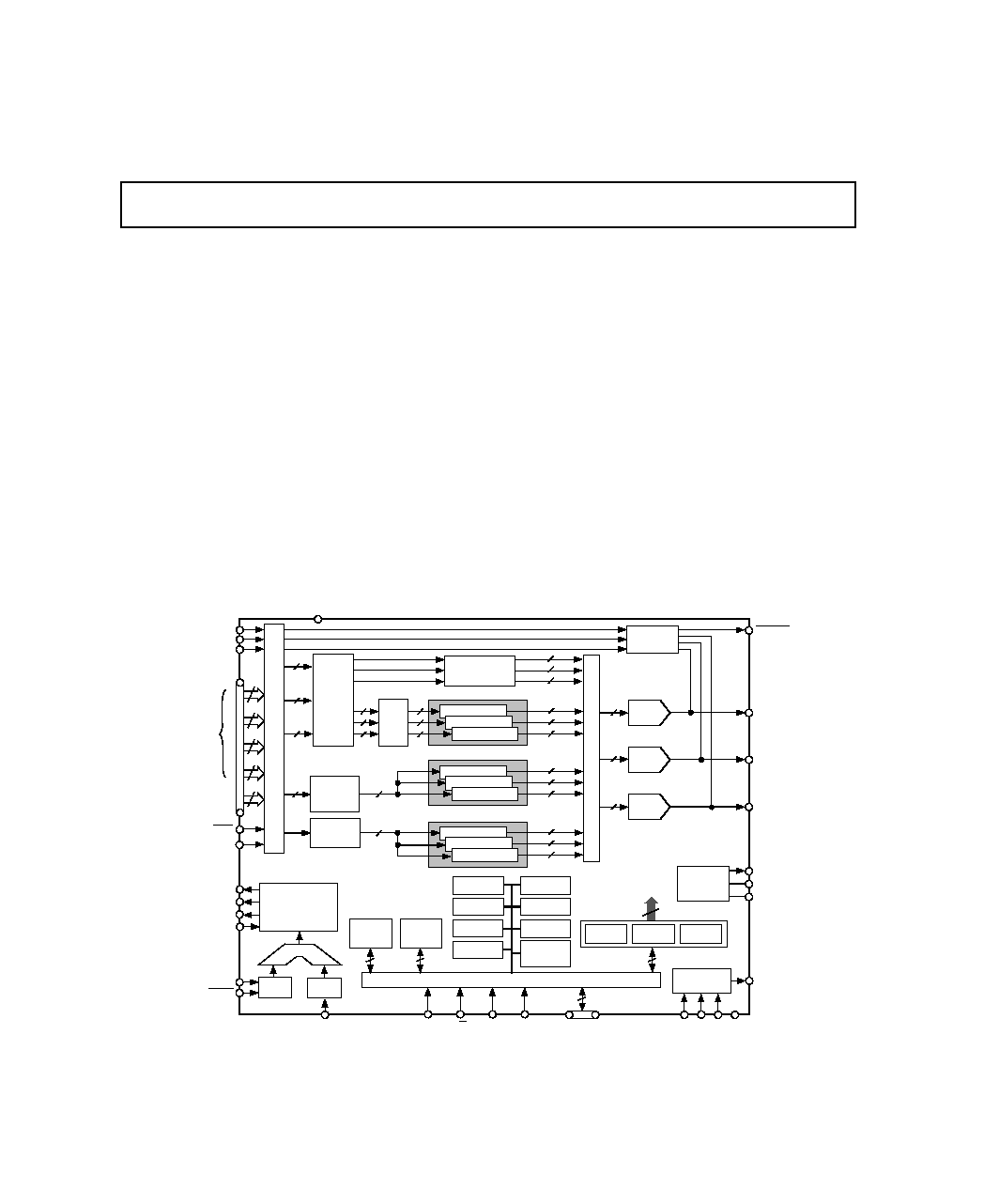
FUNCTIONAL BLOCK DIAGRAM
ADV is a registered trademark of Analog Devices, Inc.
P
I
X
E
L
I
N
P
U
T
M
U
L
T
I
P
L
E
X
E
R
JTAG TEST
ACCESS PORT
TDO
MPU PORT
10 (8+2)
DATA TO
PALETTES
30
CONTROL
REGISTERS
PIXEL MASK
REGISTER
COMMAND
REGISTERS
(CR1-CR5)
GND
TDI
TCK
TMS
C1
D9D0
C0
PIXEL
DATA
(P7-P0)
ODD/
EVEN
LOADIN
SCKIN
LOADOUT
COMP
CLOCK CONTROL
3 x 256 COLOR PALETTE
3 COLOR OVERLAY PALETTE
IOG
IOB
ECL TO
CMOS
PLL
PLL
REF
CLOCK
A
PALETTE
SELECTS
(PS0, PS1)
SYNCOUT
IOR
CLOCK
PRGCKOUT
SCKOUT
SELECTOR
ADDRESS
REGISTER
(A10-A0)
TRISYNC
SYNC
BLANK
B
C
D
S
E
L
E
C
T
O
R
CE
R/
W
GREEN
REGISTER
BLUE
REGISTER
RED
REGISTER
ADV7160/
ADV7162
2 COLOR CURSOR PALETTE
MODE
REGISTER
(MR1)
10
10
10
2
2
10
BYPASS COLOR
MODE MATRIX
10
10
10
8
8
8
8
8
8
PIXEL
MASK
COLOR
MODE
MATRIX
10
10
10
RED 256 x 10
GREEN 256 x 10
BLUE 256 x 10
RED 3 x 10
GREEN 3 x 10
BLUE 3 x 10
24
24
24
24
8
8
8
8
PS
FUNCTION
DECODE
LOGIC
2
10
10
10
RED 3 x 10
GREEN 3 x 10
BLUE 3 x 10
64 x 64
CURSOR
GENERATOR
10
10
10
GREEN
DAC
BLUE
DAC
RED
DAC
BLANK AND
SYNC LOGIC
V
REF
R
SET
10
10
CLOCK DIVIDE &
SYNCHRONIZATION
CIRCUITRY
÷
32,
÷
16,
÷
8,
÷
4
VOLTAGE
REFERENCE
CIRCUIT
REVISION
REGISTER
PLL
REGISTERS
CURSOR
REGISTERS
TEST
REGISTERS
ID
REGISTER
STATUS
REGISTER
V
AA
ADV7160/ADV7162SPECIFICATIONS
REV. 0
2
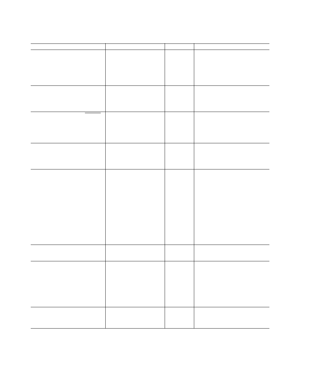
Parameter
Min
Typ
Max
Units
Test Conditions/Comments
STATIC PERFORMANCE
(DAC Gain Setting = 3996)
Resolution (Each DAC)
10
Bits
Accuracy (Each DAC)
Integral Nonlinearity
±
1
LSB
Differential Nonlinearity
±
1
LSB
Guaranteed Monotonic
Gray Scale Error
±
5
% Gray Scale
Coding
Binary
DIGITAL INPUTS
Input High Voltage, V
INH
2
V
Input Low Voltage, V
INL
0.8
V
Input Current, I
IN
±
10
µ
A
V
IN
= 0.4 V or 2.4 V
Input Capacitance, C
IN
10
pF
CLOCK INPUTS (CLOCK, CLOCK)
Input High Voltage, V
INH
V
AA
1.0
V
Input Low Voltage, V
INL
V
AA
1.6
V
Input Current, I
IN
±
10
µ
A
V
IN
= 0.4 V or 2.4 V
Input Current, I
IN
(JTAG Inputs)
±
50
µ
A
V
IN
= 0.4 V or 2.4 V
Input Capacitance, C
IN
10
pF
DIGITAL OUTPUTS
Output High Voltage, V
OH
2.4
V
I
SOURCE
= 400
µ
A
Output Low Voltage, V
OL
0.4
V
I
SINK
= 3.2 mA
Floating-State Leakage Current
20
µ
A
Floating-State Output Capacitance
20
pF
ANALOG OUTPUTS
(DAC Gain Setting = 3996)
Gray Scale Current Range
15
22
mA
Output Current
White Level Relative to Blank
17.69
19.05
20.40
mA
White Level Relative to Black
16.74
17.62
18.50
mA
Black Level Relative to Blank
0.95
1.44
1.90
mA
Blank Level
0
5
50
µ
A
Sync Disabled
Blank Level
6.29
7.62
8.96
mA
Sync Enabled
Sync Level
0
5
50
µ
A
Tri-Sync Level Relative to Blank
6.29
7.62
8.96
mA
LSB Size
17.22
µ
A
DAC to DAC Matching
1
3
%
Output Compliance, V
OC
0
+1.4
V
Output Impedance, R
OUT
30
k
Output Capacitance, C
OUT
30
pF
I
OUT
= 0 mA
VOLTAGE REFERENCE
Voltage Reference Range, V
REF
1.14
1.235
1.26
V
V
REF
= 1.235 V for Specified Performance
Input Current, I
VREF
5
µ
A
POWER REQUIREMENTS
V
AA
5
V
I
AA
3
475
mA
For 220 MHz Operation (ADV7160)
440
mA
For 170 MHz Operation (ADV7160)
410
mA
For 140 MHz Operation (ADV7160)
I
AA
3
450
mA
For 220 MHz Operation (ADV7162)
400
mA
For 170 MHz Operation (ADV7162)
360
mA
For 140 MHz Operation (ADV7162)
Power Supply Rejection Ratio
0.1
%/%
COMP = 0.1
µ
F
DYNAMIC PERFORMANCE
Clock and Data Feedthrough
4, 5
30
dB
Glitch Impulse
50
pV secs
DAC to DAC Crosstalk
6
23
dB
NOTES
1
±
5% for all versions.
2
Temperature range (T
MIN
to T
MAX
): 0
°
C to +70
°
C.
3
Pixel Port is continuously clocked with data corresponding to a linear ramp. T
J
= 100
o
C.
4
Clock and data feedthrough is a function of the amount of overshoot and undershoot on the digital inputs. Glitch impulse includes clock and data feedthrough.
5
TTL input values are 0 V to 3 V, with input rise/fall times
3 ns, measured the 10% and 90% points. Timing reference points at 50% for inputs and outputs.
6
DAC to DAC Crosstalk is measured by holding one DAC high while the other two are making low to high and high to low transitions.
Specifications subject to change without notice.
(V
AA
1
= +5 V; V
REF
= +1.235 V; R
SET
= 280
. IOR, IOG, IOB (R
L
= 37.5
,
C
L
= 10 pF). All specifications T
MIN
to T
MAX
2
unless otherwise noted.)
ADV7160/ADV7162
REV. 0
3
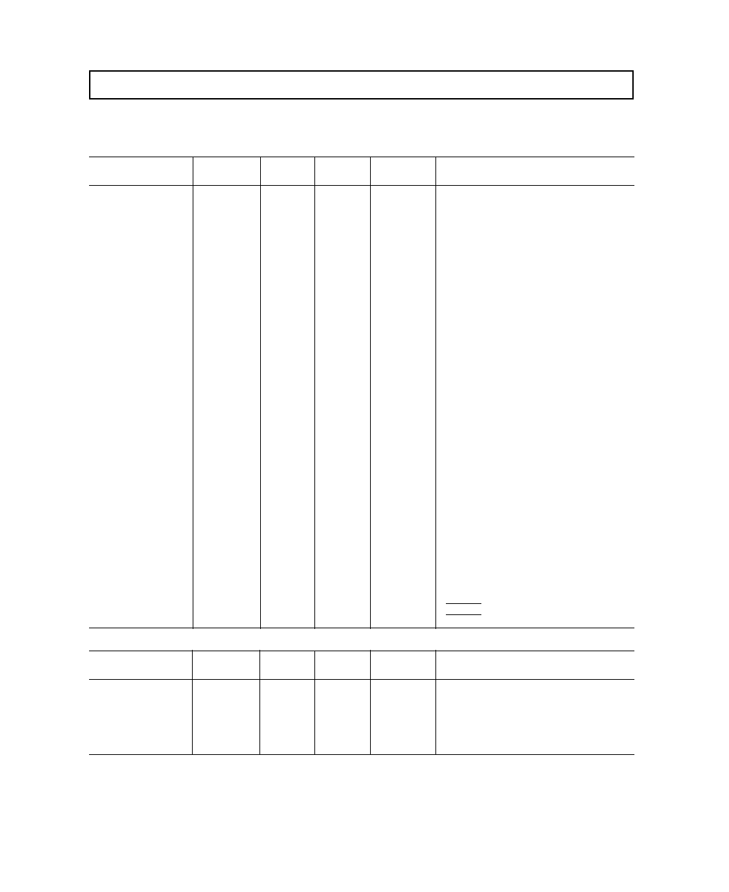
CLOCK CONTROL AND PIXEL PORT
4
Parameter
220 MHz
170 MHz
140 MHz
Units
Conditions/Comments
Version
Version
Version
f
CLOCK
220
170
140
MHz max
Pixel CLOCK Rate
t
1
4.5
5.88
7.14
ns min
Pixel CLOCK Cycle Time
t
2
2.0
2.5
2.86
ns min
Pixel CLOCK High Time
t
3
2.0
2.5
2.86
ns min
Pixel CLOCK Low Time
t
4
10
10
10
ns max
Pixel CLOCK to LOADOUT Delay
f
LOADIN
LOADIN Clocking Rate
2:1 Multiplexing
110
85
70
MHz max
4:1 Multiplexing
55
42.5
35
MHz max
8:1 Multiplexing
27.5
21.25
17.5
MHz max
t
5
LOADIN Cycle Time
2:1 Multiplexing
9.1
11.77
14.29
ns min
4:1 Multiplexing
18.18
23.53
28.58
ns min
8:1 Multiplexing
36.36
47.1
57.16
ns min
t
6
LOADIN High Time
2:1 Multiplexing
4
5
6
ns min
4:1 Multiplexing
8
9
12
ns min
8:1 Multiplexing
15
18
23
ns min
t
7
LOADIN Low Time
2:1 Multiplexing
4
5
6
ns min
4:1 Multiplexing
8
9
12
ns min
8:1 Multiplexing
15
18
23
ns min
t
8
0
0
0
ns min
Pixel Data Setup Time
t
9
5
5
5
ns min
Pixel Data Hold Time
t
10
0
0
0
ns min
LOADOUT to LOADIN Delay
-t
11
5
-5
-5
-5
ns max
LOADOUT to LOADIN Delay
t
PD
6
Pipeline Delay
2:1 Multiplexing
9
9
9
CLOCKs
(1
×
CLOCK = t
1
)
4:1 Multiplexing
11
11
11
CLOCKs
8:1 Multiplexing
15
15
15
CLOCKs
t
12
10
10
10
ns max
Pixel CLOCK to PRGCKOUT Delay
t
13
5
5
5
ns max
SCKIN to SCKOUT Delay
t
14
5
5
5
ns min
BLANK
to SCKIN Setup Time
t
15
0
0
0
ns min
BLANK
to SCKIN Hold Time
ANALOG OUTPUTS
7
Parameter
220 MHz
170 MHz
140 MHz
Units
Conditions/Comments
Version
Version
Version
t
16
25
25
25
ns typ
Analog Output Delay
t
17
1
1
1
ns typ
Analog Output Rise/Fall Time
t
18
25
25
25
ns typ
Analog Output Transition Time
t
SK
2
2
2
ns max
RGB Analog Output Skew
0
0
0
ns typ
TIMING CHARACTERISTICS
1
(V
AA
2
= +5 V; V
REF
= +1.235 V; R
SET
= 280
. IOR, IOG, IOB (R
L
= 37.5
, C
L
= 10 pF). All
specifications T
MIN
to T
MAX
3
unless otherwise noted.)
REV. 0
4
ADV7160/ADV7162
MPU P
ORT
8,9
Parameter
220 MHz
170 MHz
140 MHz
Units
Conditions/Comments
Version
Version
Version
t
19
0
0
0
ns min
R/W, C0, C1 to CE Setup Time
t
20
10
10
10
ns min
R/W, C0, C1 to CE Hold Time
t
21
45
45
45
ns min
CE
Low Time
t
22
25
25
25
ns min
CE
High Time
t
23
8
5
5
5
ns min
CE
Asserted to Data-Bus Driven
t
24
9
45
45
45
ns max
CE
Asserted to Data Valid
t
25
9
20
20
20
ns max
CE
Disabled to Data-Bus Three-Stated
t
26
9
5
5
5
ns min
CE
Disabled to Data Invalid
t
27
20
20
20
ns min
Write Data (D0D9) Setup Time
t
28
5
5
5
ns min
Write Data (D0D9) Hold Time
NOTES
General Notes
1
TTL input values are 0 to 3 volts, with input rise/fall times
3 ns, measured between the 10% and 90% points.
ECL inputs (CLOCK, CLOCK) are V
AA
0.8 V to V
AA
1.8 V, with input rise/fall times
2 ns, measured between the 10% and 90% points.
Timing reference points at 50% for inputs and outputs.
Analog output load
10 pF.
Data-Bus (D0D9) loaded as shown in Figure 1.
Digital output load for LOADOUT, PRGCKOUT & SCKOUT
30 pF.
2
±
5% for all versions
3
Temperature range (T
MIN
to T
MAX
); 0
°
C to +70
°
C.
Notes on PIXEL PORT
4
Pixel Port consists of the following inputs:
Pixel Inputs:
RED [A, B, C, D]
GREEN [A, B, C, D]
BLUE [A, B, C, D]
Palette Selects:
PS0 [A, B, C, D];
PS1[A, B, C, D]
Pixel Controls:
SYNC
, BLANK, TRISYNC, ODD/EVEN
Clock Inputs:
CLOCK, CLOCK, LOADIN, SCKIN
Clock Outputs:
LOADOUT, PRGCKOUT, SCKOUT
5
is the LOADOUT Cycle Time and is a function of the Pixel CLOCK Rate and the Multiplexing Mode:
2:1 multiplexing;
= CLOCK
×
2
= 2
×
t
1
ns
4:1 multiplexing;
= CLOCK
×
4
= 4
×
t
1
ns
8:1 multiplexing;
= CLOCK
×
8
= 8
×
t
1
ns
6
These fixed values for Pipeline Delay are valid under conditions where t
10
and
-t
11
are met. If either t
10
or
-t
11
are not met, the part will operate but the Pipeline
Delay is increased.
Notes on ANALOG OUTPUTS
7
Output delay measured from the 50% point of the rising edge of CLOCK to the 50% point of full-scale transition.
Output rise/fall time measured between the 10% and 90% points of full-scale transition.
Transition time measured from the 50% point of full scale transition to the output remaining within 2% of the final output value. (Transition time does not include
clock and data feedthrough).
Notes on MPU PORT
8
t
23
and t
24
are measured with the load circuit of Figure 1 and defined as the time required for an output to cross 0.4 V or 2.4 V.
9
t
25
and t
26
are derived from the measured time taken by the data outputs to change by 0.5 V when loaded with the circuit of Figure 1. The measured numbers are
then extrapolated back to remove the effects of charging the 100 pF capacitor. This means that the times t
25
and t
26
, quoted in the Timing Characteristics are the
true values for the device and as such are independent of external loading capacitances.
Specifications subject to change without notice.
100pF
TO OUTPUT
PIN
I
SOURCE
I
SINK
+2.1V
Figure 1. Load Circuit for Databus Access and Relinquish Times
ADV7160/ADV7162
REV. 0
5
JTAG P
ORT
Parameter
All Versions
Units
Conditions/Comments
PLL PERFORMANCE
4
Jitter
250
ps rms
1
PLL REFERENCE INPUT
PLL
REF
Frequency
900
kHz min
40
MHz max
V
IH
2.0
V max
V
IL
0.8
V min
PLL
REF
Period
25
ns min
1.67
µ
s max
PLL
REF
Duty Cycle
40
% min
60
% max
JTAG PERFORMANCE
TCK Frequency, t
29
20
MHz max
TCK High Time, t
30
15
ns min
TCK
Low Time, t
31
15
ns min
TDI, TMS Setup Time, t
32
15
ns max
TDI, TMS Hold Time, t
33
15
ns max
Digital Input to TCK Setup Time, t
34
15
ns max
Digital Input to TCK Hold Time, t
35
15
ns max
TCLK to TDO Drive, t
36
0
ns min
TCLK to TDO Valid, t
37
20
ns min
TCLK to TDO Three-State, t
38
5
ns min
15
ns max
NOTES
1
TTL input values are 0 to 3 volts, with input rise/fall times
3 ns, measured between the 10% and 90% points. Timing reference points at 50% for inputs and outputs.
2
±
5% for all versions.
3
Temperature range (T
MIN
to T
MAX
); 0
°
C to +70
°
C.
4
Jitter is measured by triggering on the output clock, delayed by 15
µ
s and then measuring the time period from the trigger edge to the next edge of the output clock
after the delay. This measurement is repeated multiple times and the RMS value is determined.
Specifications subject to change without notice.
t
38
t
36
t
37
t
35
t
34
t
33
t
30
t
32
t
29
t
31
TCK
TMS, TDI
DIGITAL
INPUT
TDO
TDO
Figure 2. JTAG Timing
TIMING CHARACTERISTICS (Cont.)
1
(V
AA
2
= +5 V; V
REF
= +1.235 V; R
SET
= 280
. IOR, IOG, IOB (R
L
= 37.5
, C
L
=10 pF).
All specifications T
MIN
to T
MAX
3
unless otherwise noted.)
REV. 0
6
ADV7160/ADV7162
Timing Waveforms
CLOCK
CLOCK
LOADOUT
(2:1 MULTIPLEXING)
LOADOUT
(4:1 MULTIPLEXING)
LOADOUT
(8:1 MULTIPLEXING)
t
4
t
2
t
3
t
1
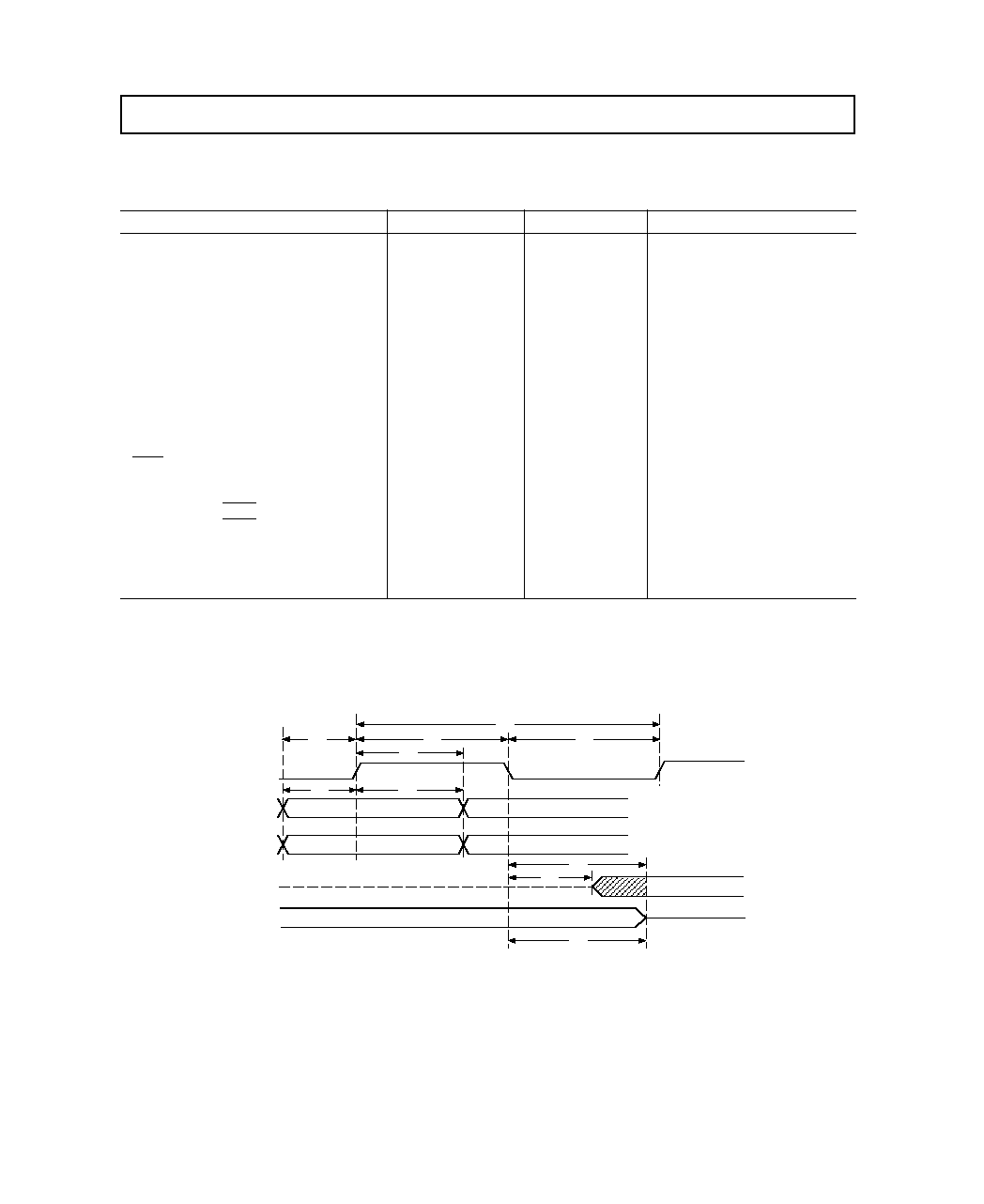
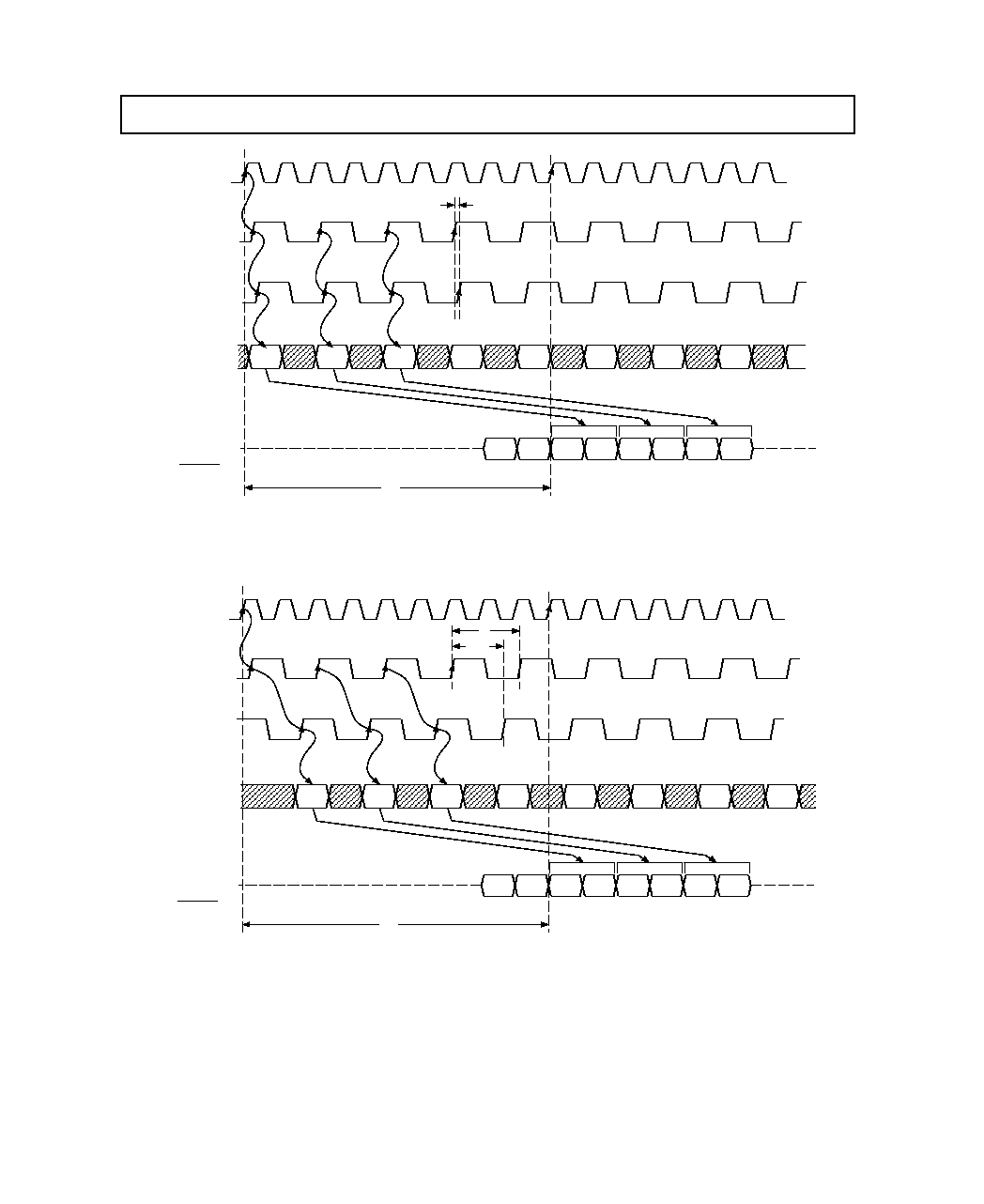
Figure 3. LOADOUT vs. Pixel Clock Input (CLOCK, CLOCK)
t
5
t
6
t
7
t
8
t
9
VALID
DATA
VALID
DATA
VALID
DATA
LOADIN
PIXEL INPUT
DATA
Figure 4. LOADIN vs. Pixel Input Data
ADV7160/ADV7162
REV. 0
7
t
10
A
N
...
H
N
A
N+1
...
H
N+1
A
N+2
...
H
N+2
DIGITAL INPUT TO ANALOG
OUTPUT PIPELINE
A
N+2
... H
N+2
A
N+1
... H
N+1
A
N
... H
N
A
N1
... H
N1
t
PD
CLOCK
LOADOUT
LOADIN
PIXEL
INPUT
DATA
ANALOG
OUTPUT
DATA
(IOR, IOG, IOB,
SYNCOUT
)
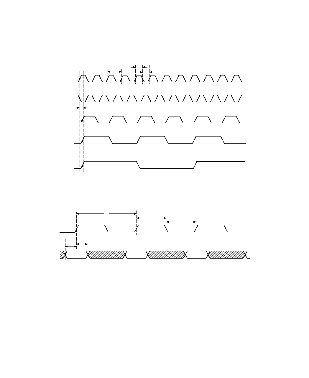
Figure 5. Pixel Input to Analog Output Pipeline with Minimum LOADOUT to LOADIN Delay (8:1 Multiplex Mode)
A
N
...
H
N
A
N+1
...
H
N+1
A
N+2
...
H
N+2
DIGITAL INPUT TO ANALOG
OUTPUT PIPELINE
A
N+2
... H
N+2
A
N+1
... H
N+1
A
N
... H
N
A
N1
... H
N1
t
PD
CLOCK
LOADOUT
LOADIN
PIXEL
INPUT
DATA
ANALOG
OUTPUT
DATA
(IOR, IOG, IOB,
SYNCOUT
)
-
t
11
Figure 6. Pixel Input to Analog Output Pipeline with Maximum LOADOUT to LOADIN Delay (8:1 Multiplex Mode)
REV. 0
8
ADV7160/ADV7162
t
10
A
N
...
D
N
A
N+1
...
D
N+1
A
N+2
...
D
N+2
DIGITAL INPUT TO ANALOG
OUTPUT PIPELINE
A
N+2
... D
N+2
A
N+1
... D
N+1
A
N
... D
N
A
N1
... D
N1
t
PD
CLOCK
LOADOUT
LOADIN
PIXEL
INPUT
DATA
ANALOG
OUTPUT
DATA
(IOR, IOG, IOB,
SYNCOUT
)
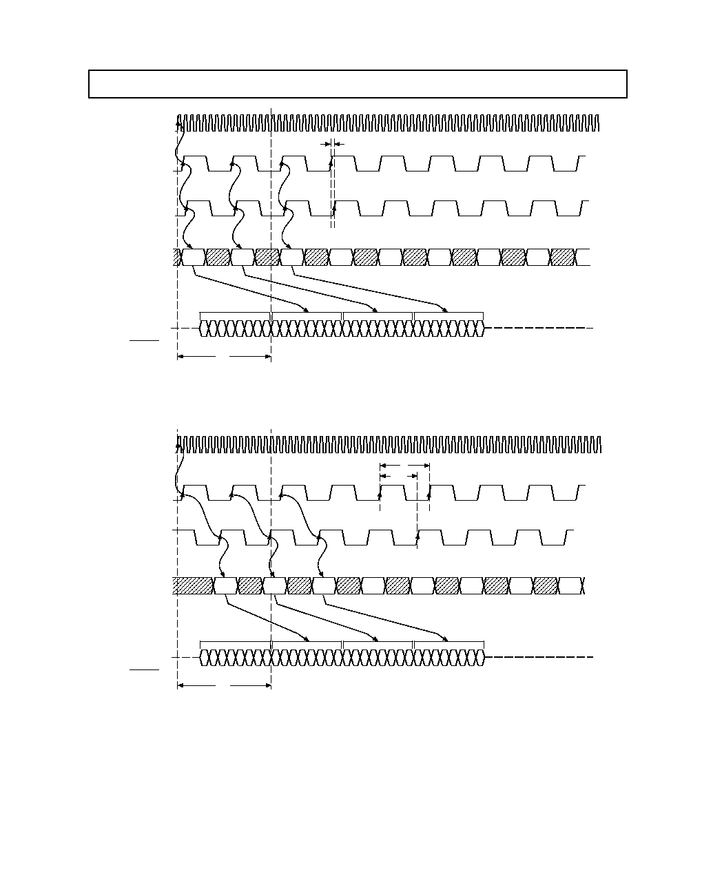
Figure 7. Pixel Input to Analog Output Pipeline with Minimum LOADOUT to LOADIN Delay (4:1 Multiplex Mode)
A
N
...
D
N
A
N+1
...
D
N+1
A
N+2
...
D
N+2
DIGITAL INPUT TO ANALOG
OUTPUT PIPELINE
A
N+2
... D
N+2
A
N+1
... D
N+1
A
N
... D
N
A
N1
... D
N1
t
PD
CLOCK
LOADOUT
LOADIN
PIXEL
INPUT
DATA
-
t
11
ANALOG
OUTPUT
DATA
(IOR, IOG, IOB,
SYNCOUT
)
Figure 8. Pixel Input to Analog Output Pipeline with Maximum LOADOUT to LOADIN Delay (4:1 Multiplex Mode)
ADV7160/ADV7162
REV. 0
9
t
10
A
N
...
B
N
A
N+1
...
B
N+1
A
N+2
...
B
N+2
t
PD
CLOCK
LOADOUT
LOADIN
PIXEL
INPUT
DATA
DIGITAL INPUT TO ANALOG OUTPUT PIPELINE
A
N1
B
N1
A
N
B
N
A
N+1
B
N+1
A
N+2
BN+2
ANALOG
OUTPUT
DATA
(IOR, IOG, IOB,
SYNCOUT
)
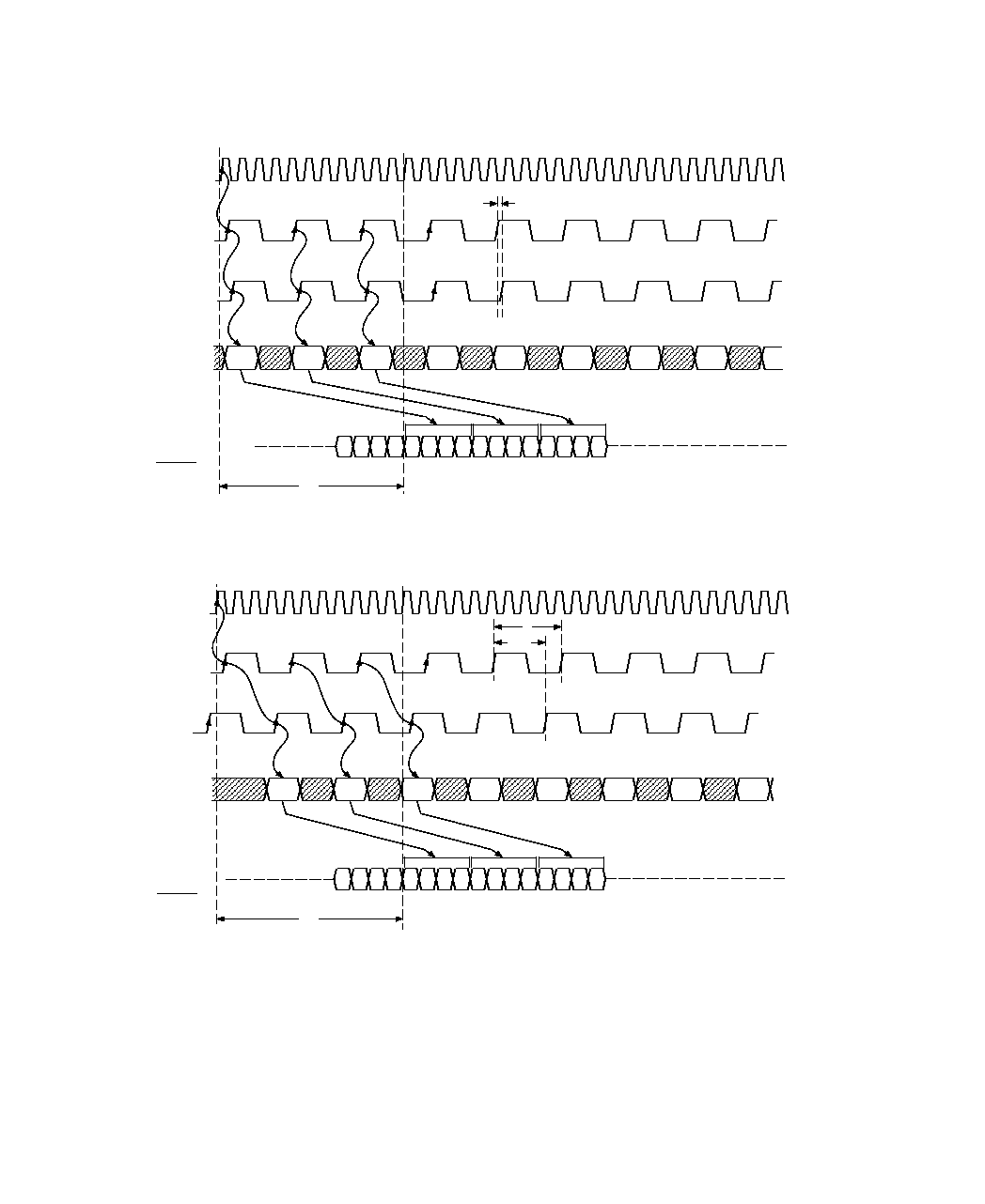
Figure 9. Pixel Input to Analog Output Pipeline with Minimum LOADOUT to LOADIN Delay (2:1 Multiplex Mode)
A
N
...
B
N
A
N+1
...
B
N+1
A
N+2
...
B
N+2
t
PD
CLOCK
LOADOUT
LOADIN
PIXEL
INPUT
DATA
DIGITAL INPUT TO ANALOG OUTPUT PIPELINE
A
N1
B
N1
A
N
B
N
A
N+1
B
N+1
A
N+2
B
N+2
-t
10
ANALOG
OUTPUT
DATA
(IOR, IOG, IOB,
SYNCOUT
)
Figure 10. Pixel Input to Analog Output Pipeline with Maximum LOADOUT to LOADIN Delay (2:1 Multiplex Mode)
REV. 0
10
ADV7160/ADV7162
CLOCK
t
12
PRGCKOUT
(CLOCK/4)
PRGCKOUT
(CLOCK/8)
PRGCKOUT
(CLOCK/16)
PRGCKOUT
(CLOCK/32)
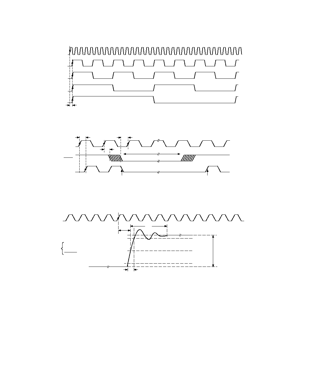
Figure 11. Pixel Clock Input vs. Programmable Clock Output (PRGCKOUT)
t
13
t
15
t
14
SCKIN
BLANK
SCKOUT
BLANKING PERIOD
END OF SCAN LINE (N)
START OF SCAN LINE (N+1)
Figure 12. Video Data Shift Clock Input (SCKIN) & BLANK vs. Video Data Shift Clock Output (SCKOUT)
t
17
t
18
IOR
IOG
IOB
SYNCOUT
ANALOG
OUTPUTS
CLOCK
NOTE:
THIS DIAGRAM IS NOT TO SCALE. FOR THE PURPOSES OF CLARITY, THE
ANALOG OUTPUT WAVEFORM IS MAGNIFIED IN TIME AND AMPLLITUDE
W.R.T THE CLOCK WAVEFORM.
SYNCOUT IS A DIGITAL VIDEO OUTPUT SIGNAL.
t
16
IS THE ONLY RELEVANT TIMING SPECIFICATION FOR SYNCOUT.
WHITE LEVEL
BLACK LEVEL
FULL SCALE
TRANSITION
90%
50%
10%
t
16
Figure 13. Analog Output Response vs. CLOCK
ADV7160/ADV7162
REV. 0
11
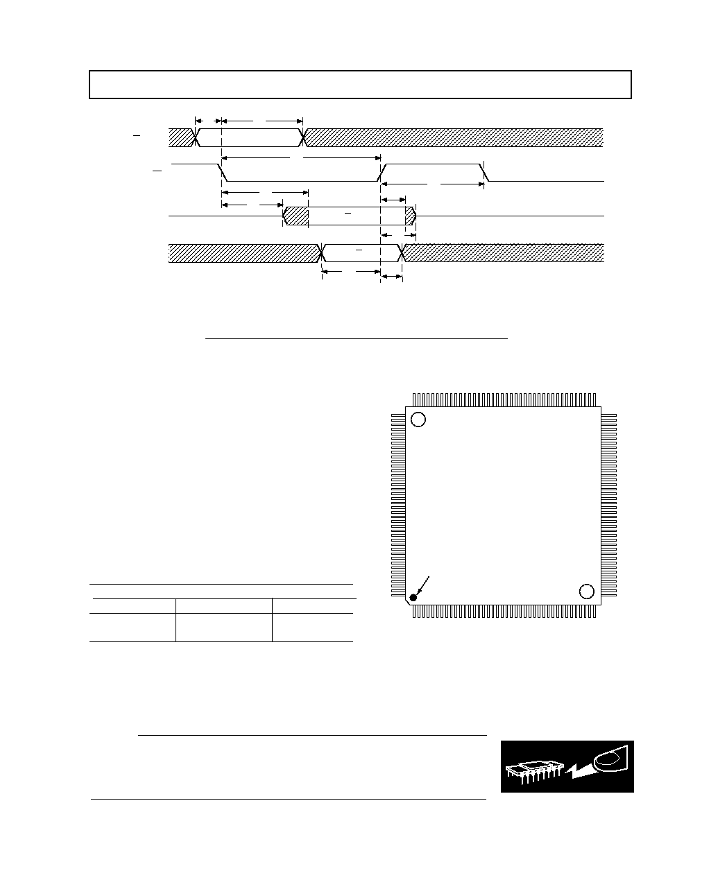
VALID
CONTROL DATA
t
27
t
28
t
26
t
25
R/
W
= 1
R/
W
= 0
R/
W
, C0, C1
CE
D0D9
(READ MODE)
D0D9
(WRITE MODE)
t
21
t
24
t
23
t
22
t
20
t
19
Figure 14. Microprocessor Port (MPU) Interface Timing
ABSOLUTE MAXIMUM RATINGS
1
V
AA
to GND . . . . . . . . . . . . . . . . . . . . . . . . . . . . . . . . . . . . 7 V
Voltage on Any Digital Pin . . . . . GND 0.5 V to V
AA
+ 0.5 V
Ambient Operating Temperature (T
A
) . . . . . . . . 0
°
C to +70
°
C
Storage Temperature (T
S
) . . . . . . . . . . . . . . . 65
°
C to +150
°
C
Junction Temperature (T
J
) . . . . . . . . . . . . . . . . . . . . . +150
°
C
Lead Temperature (Soldering, 10 secs) . . . . . . . . . . . . +260
°
C
Vapor Phase Soldering (1 minute) . . . . . . . . . . . . . . . . +220
°
C
Analog Outputs to GND
2
. . . . . . . . . . . . GND 0.5 V to V
AA
NOTES
1
Stresses above those listed under "Absolute Maximum Ratings" may cause
permanent damage to the device. This is a stress rating only and functional
operation of the device at these or any other conditions above those listed in the
operational sections of this specification is not implied. Exposure to absolute
maximum rating conditions for extended periods may affect device reliability.
2
Analog Output Short Circuit to any Power Supply or Common can be of an
indefinite duration.
160-Lead QFP Configuration
PIN NO. 1
IDENTIFIER
ROW A
ROW C
ROW D
ROW B
80
41
121
160
120
81
1
40
ADV7160/ADV7162
QFP
TOP VIEW
(NOT TO SCALE)
WARNING!
ESD SENSITIVE DEVICE
CAUTION
ESD (electrostatic discharge) sensitive device. Electrostatic charges as high as 4000 V readily
accumulate on the human body and test equipment and can discharge without detection.
Although the ADV7160/ADV7162 features proprietary ESD protection circuitry, permanent
damage may occur on devices subjected to high energy electrostatic discharges. Therefore, proper
ESD precautions are recommended to avoid performance degradation or loss of functionality.
ORDERING INFORMATION
1, 2, 3
Dot Clock Speed
220 MHz
170 MHz
140 MHz
ADV7160KS220
3
ADV7160KS170
3
ADV7160KS140
3
ADV7162KS220
4
ADV7162KS170
4
ADV7162KS140
4
NOTES
1
All devices are specified for 0
°
C to +70
°
C operation.
2
Contact Sales Office for latest information on package design.
3
ADV7160 is packaged in a 160-pin plastic power quad flatpack, QFP with
heatsink embedded.
4
ADV7162 is packaged in a standard 160-pin plastic quad flatpack, QFP.
REV. 0
12
ADV7160/ADV7162
ADV7160/ADV7162 PIN ASSIGNMENTS
Pin No.
Mnemonic
Pin No.
Mnemonic
Pin No.
Mnemonic
Pin No.
Mnemonic
1
G2
A
41
CLOCK
81
D9
121
R1
C
2
G2
B
42
SCKIN
82
D8
122
R1
D
3
G2
C
43
SCKOUT
83
D7
123
R2
A
4
G2
D
44
V
AA
84
D6
124
R2
B
5
G3
A
45
PRGCKOUT
85
D5
125
R2
C
6
G3
B
46
GND
86
D4
126
R2
D
7
G3
C
47
LOADOUT
87
D3
127
R3
A
8
G3
D
48
LOADIN
88
D2
128
R3
B
9
G4
A
49
B0
A
89
D1
129
R3
C
10
G4
B
50
B0
B
90
D0
130
R3
D
11
G4
C
51
B0
C
91
C1
131
R4
A
12
G4
D
52
B0
D
92
C0
132
V
AA
13
G5
A
53
B1
A
93
R/W
133
V
AA
14
G5
B
54
B1
B
94
CE
134
GND
15
G5
C
55
B1
C
95
TCK
135
GND
16
G5
D
56
B1
D
96
TMS
136
R4
B
17
G6
A
57
B2
A
97
GND
137
R4
C
18
G6
B
58
B2
B
98
V
AA
138
R4
D
19
G6
C
59
B2
C
99
TDO
139
R5
A
20
G6
D
60
B2
D
100
TDI
140
R5
B
21
G7
A
61
B3
A
101
SYNCOUT
141
R5
C
22
V
AA
62
B3
B
102
TRISYNC
142
R5
D
23
V
AA
63
B3
C
103
ODD/EVEN
143
R6
A
24
GND
64
B3
D
104
SYNC
144
R6
B
25
GND
65
B4
A
105
BLANK
145
R6
C
26
V
AA
66
B4
B
106
V
REF
146
R6
D
27
GND
67
B4
C
107
IOB
147
R7
A
28
PLL
REF
68
B4
D
108
COMP
148
R7
B
29
G7
B
69
B5
A
109
R
SET
149
R7
C
30
G7
C
70
B5
B
110
V
AA
150
GND
31
G7
D
71
B5
C
111
V
AA
151
V
AA
32
PS0
A
72
B5
D
112
GND
152
R7
D
33
PS0
B
73
B6
A
113
IOG
153
G0
A
34
PS0
C
74
B6
B
114
IOR
154
G0
B
35
PS0
D
75
B6
C
115
R0
A
155
G0
C
36
PS1
A
76
B6
D
116
R0
B
156
G0
D
37
PS1
B
77
B7
A
117
R0
C
157
G1
A
38
PS1
C
78
B7
B
118
R0
D
158
G1
B
39
PS1
D
79
B7
C
119
R1
A
159
G1
C
40
CLOCK
80
B7
D
120
R1
B
160
G1
D

ADV7160/ADV7162
REV. 0
13
PIN FUNCTION DESCRIPTION
Mnemonic
Function
RED (R0
A
. . . R0
B
R7
A
. . . R7
D
), GREEN (G0
A
. . . G0
D
G7
A
. . . G7
D
), BLUE (B0
A
. . . B0
D
B7
A
. . . B7
D
):
Pixel Port (TTL Compatible Inputs): 96 pixel select inputs, with 8 bits each for Red, Green and Blue.
Each bit is multiplexed [A-D] 4:1 or 2:1. It can be configured for 24-Bit True-Color Data, 8-Bit
Pseudo-Color Data, 16-Bit True-Color and 15-Bit True-Color Data formats. In 8-Bit Pseudo-Color
Mode, there is a special case whereby 8:1 multiplexing is also available. It will be explained in more
detail later. Pixel Data is latched into the device on the rising edge of LOADIN.
PS0
A
. . . PS0
D
, PS1
A
. . . PS1
D
Palette Priority Selects (TTL Compatible Inputs): The eight PS inputs provide two Bits after input
multiplexing. These pixel port select inputs can be configured for three separate functions. In Overlay
Mode, these inputs provide a three color overlay function. With any value other than "00" on the
overlay inputs, the color displayed comes from the overlay palette instead of the main pixel inputs.
For the ADV7160, in Bypass Mode, PS1 specifies for each pixel whether it should pass through the
Color Matrix and Color Palette or bypass the Matrix and Palette. PS0 acts as an overlay input. (This
mode is not available for the ADV7162.) Palette Select Mode is used to multiplex the RGB outputs of
a number of devices. When the palette mode inputs match the PS bits in the mode register, the part
operates as normal. When there is a mismatch, the RGB outputs are switched to zero, allowing the
RGB outputs of another device to drive the monitor.
LOADIN
Pixel Data Load Input (TTL Compatible Input): This input latches the multiplexed pixel data, in-
cluding PS0-PS1, BLANK, TRISYNC, SYNC and ODD/EVEN into the device.
LOADOUT
Pixel Data Load Output (TTL Compatible Output): This output control signal runs at a divided
down frequency of the pixel clock. Its frequency is a function of the multiplex rate. It can be used to
directly or indirectly drive LOADIN.
f
LOADOUT
= f
CLOCK
/M
where
(M = 2 for 2:1 Multiplex Mode)
(M = 4 for 4:1 Multiplex Mode)
(M = 8 for 8:1 Multiplex Mode)
PRGCKOUT
Programmable Clock Output (TTL Compatible Output): This output control signal runs at a divided
down frequency of the pixel Clock. Its frequency is user programmable and is determined by bits
CR30 and CR31 of Command Register 3.
f
PRGCKOUT
= f
CLOCK
/N
where N = 4, 8, 16 & 32
SCKIN
Video Shift Clock Input (TTL Compatible Input): The signal on this input is internally gated syn-
chronously with the BLANK signal. The resultant output, SCKOUT, is a video clocking signal that
is stopped during video blanking periods. It is normally driven by a divided down version of the
CLOCK frequency.
SCKOUT
Video Shift Clock Output (TTL Compatible Output): This output is a synchronously gated version of
SCKIN and BLANK. SCKOUT is a video clocking signal that is stopped during video blanking
periods.
CLOCK, CLOCK
Clock Inputs (ECL Compatible Inputs): These differential clock inputs are designed to be driven by
ECL logic levels configured for single supply (+5 V) operation. The clock rate is normally the pixel
clock rate of the system.
PLL
REF
PLL Clock Input (TTL Compatible Input): This clock input is designed to be driven by TTL logic
levels. The PLL is then configured to output a specific frequency depending on the PLL Registers.
See PLL section for more detail.
BLANK
Composite Blank (TTL Compatible Input): This video control signal drives the analog outputs to the
blanking level.
SYNC
Composite-Sync Input (TTL Compatible Input): This video control signal drives any of the analog
outputs to the SYNC level. It is only asserted during the blanking period. CR22 in Command
Register 2 must be set if SYNC is to be decoded onto the IOG analog output, CR41 in Command
Register 4 must be set if SYNC is to be decoded onto the IOR analog output, CR42 in Command
Register 4 must be set if SYNC is to be decoded onto the IOB analog output, otherwise the SYNC
input is ignored.

REV. 0
14
ADV7160/ADV7162
Mnemonic
Function
SYNCOUT
Composite-Sync Output (TTL Compatible Output). This video output is a delayed version of
SYNC
. The delay corresponds to the number of pipeline stages of the device.
TRISYNC
Composite-Sync HDTV Control (TTL Compatible Output). This video input is enabled using Bit
CR17 in Command Register 1. When TRISYNC is low, any DAC output which has Sync enabled,
goes to the tri-sync level. As with the SYNC input, it should only be activated while BLANK is low.
D9D0
Data Bus (TTL Compatible Input/Output Bus). Data, including color palette values and device con-
trol information is written to and read from the device over this 10-bit, bidirectional databus. 10-bit
data or 8-bit data can be used. The databus can be configured for either 10-bit parallel data or byte
data (8+2) as well as standard 8-bit data. Any unused bits of the data bus should be terminated
through a resistor to either the digital power plane (V
CC
) or GND.
ODD/EVEN
Odd/Even Control (TTL Compatible Input). This input indicates which field of the frame is being
displayed. It is required to ensure proper operation of the ADV7160/ADV7162 cursor when inter-
laced display mode is selected. It is ignored when noninterlaced display mode is selected. This input
should change only during the vertical blank period. It is assumed that an odd field will always follow
an even field and vice versa.
CE
Chip Enable (TTL Compatible Input). This input must be at Logic "0" when writing to or reading
from the device over the data bus (D0D9). Internally, data is latched on the rising edge of CE.
R/W
Read/Write Control (TTL Compatible Input). This input determines whether data is written to or
read from the device's registers and color palette RAM. R/W and CE must be at Logic "0" to write
data to the part. R/W must be at Logic "1" and CE at Logic "0" to read from the device.
C0, C1
Command Controls (TTL Compatible Inputs). These inputs determine the type of read or write op-
eration being performed on the device over the data bus, (see Interface Truth Table). Data on these
inputs is latched on the falling edge of CE.
IOR, IOG, IOB
Red, Green & Blue Current Outputs (High Impedance Current Sources). These RGB video outputs
are specified to directly drive RS-343A and RS-170 video levels into doubly terminated 75
loads.
V
REF
Voltage Reference Input (Analog Input): An external 1.235 V voltage reference is required to drive
this input. An AD589 (2-terminal voltage reference) or equivalent is recommended. (Note: It is not
recommended to use a resistor network to generate the voltage reference.)
R
SE
T
Output Full Scale Adjust Control (Analog Input). A resistor connected between this pin and analog
ground controls the absolute amplitude of the output video signal. For a value of R
SET
of nominally
280
, with 37.5
termination and using CR43 and CR44 of Command Register 4 to set the DAC
Gain as shown, the required Video Standard can be achieved.
CR44
CR43
Video Standard
DAC Gain
Black to White
0
0
RS343A, Sync & Pedestal
3996
660 mV 17.62 mA
0
1
RS343A, Sync & No Pedestal
4224
699 mV 18.63 mA
1
0
RS343A, No Sync & No Pedestal
4311
714 mV 19.05 mA
1
1
RS170, Sync & Pedestal
5592
925 mV 24.67 mA
Alternatively, R
SET
can be calculated by the following equation:
R
SET
DAC Gain
×
V
REF
Black to White Current
COMP
Compensation Pin. A 0.1
µ
F capacitor should be connected between this pin and V
AA
.
V
AA
Power Supply (+5 V
±
5%). The part contains multiple power supply pins, all should be connected
together to one common +5 V filtered analog power supply.
GND:
Analog Ground. The part contains multiple ground pins, all should be connected together to the
system's ground plane.
TMS, TCK,
These four pins control the JTAG test access port.
TDI, TDO
See Appendix 6 for more detail
ADV7160/ADV7162
REV. 0
15
(Continued from page 1)
The ADV7160/ADV7162 integrates a number of graphic func-
tions onto one device allowing 24-bit direct True-Color (30-bit
Corrected-Color) operation at the maximum screen resolution
of 1600
×
1280 at a refresh rate of 85 Hz. The ADV7160/
ADV7162 integrates a 256
×
30 Color Palette RAM with three
high speed, 10-bit, digital-to analog converters (RGB DACs).
It also contains a user-definable, X-Windows compatible, 64
×
64
×
2 cursor generator and associated RAM. An on-board
Overlay Palette RAM is also included. The device's 96-bit Pro-
grammable Pixel Port enables various data formats to be input
to the part. An on-board clock and synchronization circuit
controls all clocking functions for both the part and graphics
subsystem.
There are two video data paths through the ADV7160/ADV7162.
One routes the data from the pixel port through the RAM to the
DACs, the other bypasses the RAM and routes data direct from
the pixel port to the DACs. Either path can be selected on a
pixel by pixel basis. This allows for the overlay of an active
video window on a graphics background.
The on-board palette priority select inputs enable multiple pal-
ette devices to be connected together for use in multipalette and
window applications. The part is controlled and programmed
through the microprocessor (MPU) port.
one TTL input signal PLL
REF
are required to get the part
operational. No additional signals or external glue logic are re-
quired to get the Pixel Port and Clock Control Circuit of the
part operational.
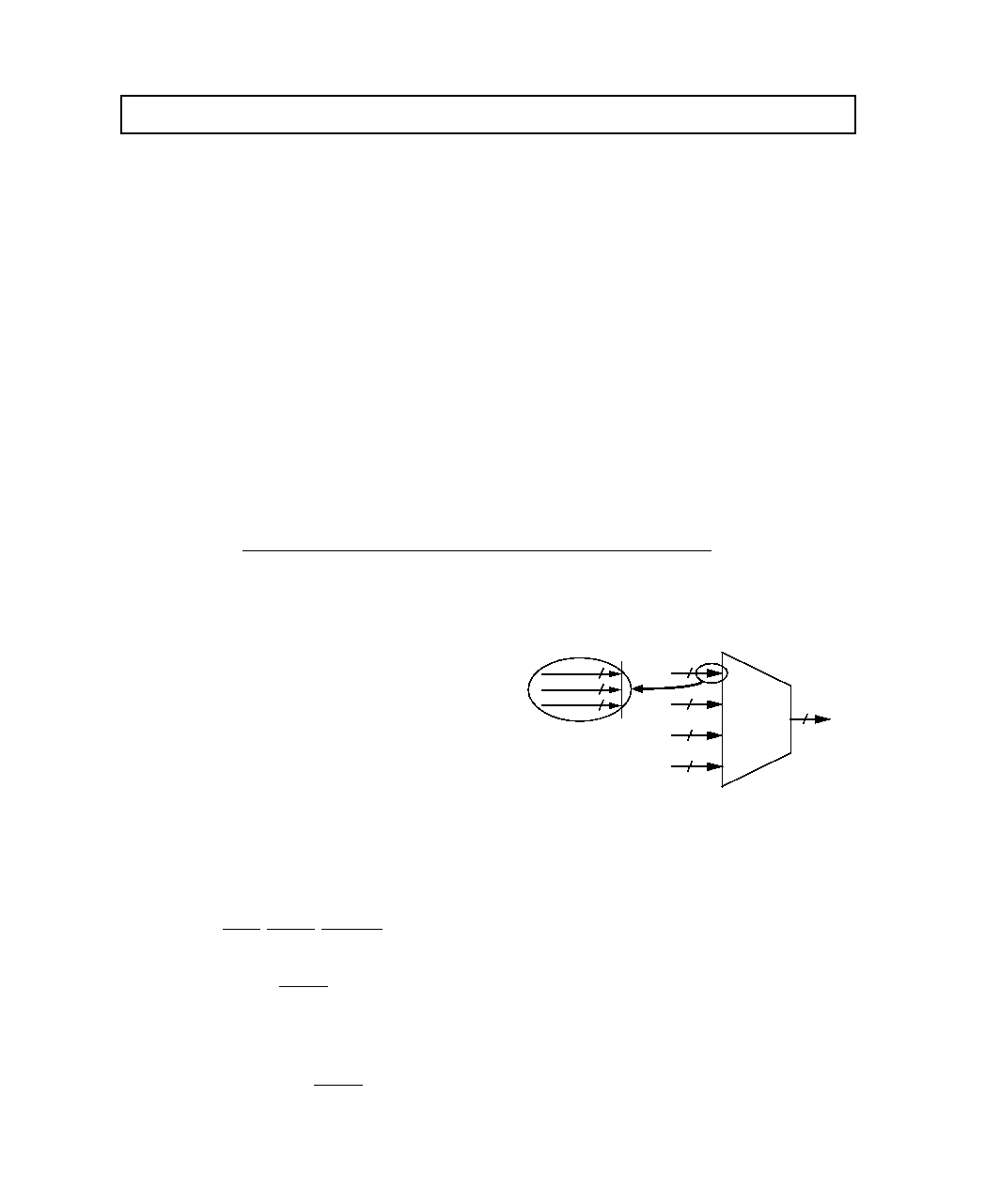
MULTIPLEXER
24
24
24
24
24
8
8
8
RED
GREEN
BLUE
A
B
C
D
Figure 15. Multiplexed Color Inputs for the
ADV7160/ADV7162
Pixel Port (Color Data)
The ADV7160/ADV7162 has 96 color data inputs. The part
has four (for 4:1 multiplexing) 24-bit wide direct color data in-
puts. These are user programmed to support a number of color
data formats including 24-bit True-Color, 16-bit True-Color,
15-bit True-Color in 4:1 and 2:1 multiplex modes, and 8-bit
Pseudo-Color (see "Multiplexing" section) in 8:1, 4:1 and 2:1
multiplex modes.
Color data is latched into the parts pixel port on every rising
edge of LOADIN (see Timing Waveform, Figure 4). The
required frequency of LOADIN is determined by the multiplex
rate, where
f
LOADIN
= f
CLOCK
/8
8:1 multiplex mode
f
LOADIN
= f
CLOCK
/4
4:1 multiplex mode
f
LOADIN
= f
CLOCK
/2
2:1 multiplex mode
CIRCUIT DETAILS AND
OPERATION
OVERVIEW
Digital video or pixel data is latched into the ADV7160/ADV7162
over the devices Pixel Port. This data acts as a pointer to on-
board Color Palette RAM. The data at the RAM address pointed
to is latched to the digital-to-analog converters (DACs) and out-
put as an RGB analog video signal.
For the purposes of clarity of description, the ADV7160/ADV7162
is broken down into three separate functional blocks. These are:
1. Pixel Port and Clock Control Circuit
2. MPU Port, Registers and Color Palette
3. Digital-to-Analog Converters and Video Outputs
Pixel Port & Clock Control Circuit
The Pixel Port of the ADV7160/ADV7162 is directly interfaced
to the video/graphics pipeline of a computer graphics subsystem.
It is connected directly or through a gate array to the video
RAM of the systems Frame-Buffer (video memory). The pixel
port on the device consists of:
Color Data
RED, GREEN, BLUE
Pixel Controls
SYNC
, BLANK, TRISYNC
Palette Selects
PS0
A-D
, PS1
A-D
The associated clocking signals for the pixel port include:
Clock Inputs
CLOCK, CLOCK, PLL
REF
,
LOADIN, SCKIN
Clock Outputs
LOADOUT, PRGCKOUT,
SCKOUT
These on-board clock control signals are included to simplify in-
terfacing between the part and the frame buffer. Either two
control input signals CLOCK and CLOCK (ECL Levels) or
The 30 bits of resolution, associated with the color look-up table
and triple 10-bit DAC, realizes 24-bit True-Color resolution,
while also allowing for the on-board implementation of linear-
ization algorithms, such as Gamma-Correction and Monitor
Callibration. This allows effective 30-bit True-Color operation.
The on-chip video clock controller circuit generates all the inter-
nal clocking and some additional external clocking signals. The
high accuracy, low jitter on board PLL eliminates the need for
an external high speed clock generator. The PLL can be pro-
grammed to produce a pixel clock that is a multiple of the PLL
reference clock.
The ADV7162 is packaged in a standard plastic 160-pin quad
flatpack (QFP).
The ADV7160 is packaged in a plastic 160-pin power quad
flatpack (PQUAD). Superior thermal distribution is achieved by
the inclusion of a copper heatslug, within the standard package
outline, to which the die is attached. This part is ideally suited
for high performance applications where external environmental
conditions are unpredictable and uncontrollable.

REV. 0
16
ADV7160/ADV7162
Other pixel data signals latched into the device by LOADIN
include SYNC, BLANK, TRISYNC and PS0
A-D
PS1
A-D
.
Internally, data is pipelined through the part by the differential
pixel clock inputs, CLOCK and CLOCK or by the internal
pixel clock generated by the PLL on-board. The LOADIN
control signal need only have a frequency synchronous relation-
ship to the pixel CLOCK (see "Pipeline Delay & On-Board
Calibration" section). A completely phase independent
LOADIN signal can be used with the ADV7160/ADV7162,
allowing the CLOCK to occur anywhere during the LOADIN
cycle.
Alternatively, the LOADOUT signal of the ADV7160/ADV7162
can be used. LOADOUT can be connected either directly or
indirectly to LOADIN. Its frequency is automatically set to the
correct LOADIN requirement.
SYNC
, BLANK
The BLANK and SYNC video control signals drive the analog
outputs to the Blank and Sync levels respectively. These signals
are latched into the part on the rising edge of LOADIN. The
SYNC
information is encoded onto the IOG analog signal
when Bit CR22 of Command Register 2 is set to "1," the IOR
analog signal when Bit CR41 of Command Register 4 is set to
"1" and the IOB analog signal when Bit CR42 of Command
Register 4 is set to "1." The SYNC input is ignored if CR22,
CR41 and CR42 are set to logic "0."
SYNCOUT
In some applications where it is not permissible to encode
SYNC
on green (IOG), blue (IOB), or red (IOR), SYNCOUT
can be used as a separate TTL digital SYNC output. This has
the advantage over an independent (of the ADV7160/ADV7162)
SYNC
in that it does not necessitate knowing the absolute pipe-
line delay of the part. This allows complete independence
between LOADIN/Pixel Data and CLOCK. The SYNC input
is connected to the device as normal with Bit CR22 of Com-
mand Register 2, Bit CR41 of Command Register 4 and Bit
CR42 of Command Register 4 are set to "0" thereby preventing
SYNC
from being encoded onto IOG, IOR and IOB. The out-
put signal generates a TTL SYNCOUT with correct pipeline
delay which is capable of directly driving the composite SYNC
signal of a computer monitor.
TRISYNC
This input is used to generate a HDTV Sync on any of the DAC
outputs. Bit CR17 of Command Register 1 is set to "1", en-
abling TRISYNC. When TRISYNC is low, the analog output
which has Sync enabled goes to the tri-sync level.
PS0
A-D
PS1
A-D
(Palette Priority Select Inputs)
These multifunctional TTL compatible inputs can be config-
ured for three separate functions. The eight PS inputs are mul-
tiplexed to provide two bits which are used to provide one of
three different functions. The function is selected by Bit CR14
and Bit CR15 of Command Register 1.
CR15
CR14
Color Mode
0
0
Palette Select Mode
0
1
Bypass Mode Control (ADV7160 Only)
1
0
Overlay Color Mode
1
1
Ignore PS Inputs
However, in 8:1 Mode, for 8-Bit Pseudo Color, the unused Blue
Pixel Inputs are used to provide 8 extra PS inputs. The bypass
mode is unavailable in this case.
Palette Select Mode
These pixel port select inputs effectively determine whether the
devices RGB analog outputs are turned-on or shut down. When
the analog outputs are shut down, IOR, IOG and IOB are
forced to 0 mA regardless of the state of the pixel and control
data inputs. This state is determined on a pixel by pixel basis as
the PS0PS1 inputs are multiplexed in exactly the same format
as the pixel port color data. These controls allow for switching
between multiple palette devices. If the values of PS0 and PS1
match the values programmed into bits MR16 and MR17 of the
Mode Register, then the device is selected, if there is no match
the device is effectively shut down.
Bypass Mode Control (ADV7160 Only)
In this mode PS1 is used to switch between one of the color
modes through the Color Palette and one of the Palette Bypass
modes on a pixel by pixel basis. The color mode through the
palette is selected using Bits CR27CR24 of Command Regis-
ter 2. The Bypass Color Mode is selected using Bits CR17 and
CR16 of Command Register 1. PS1 then switches between the
Palette Color Mode, and the Bypass Color Mode. The PS0 in-
put continues to act as an overlay input, allowing Overlay Color
1 to be displayed.
PS0
PS1
Color Mode
0
0
Palette Color Mode (CR27CR24)
0
1
Bypass Color Mode (CR17CR16)
1
x
Overlay Color 1
This mode is not available if using the ADV7162.
Overlay Color Mode
In this mode, the PS inputs provide control for a three color
overlay. Whenever the value other than "00" is placed on the
overlay inputs, the corresponding overlay color is displayed.
When the overlay inputs contain "00" the color is specified by
the main pixel inputs.
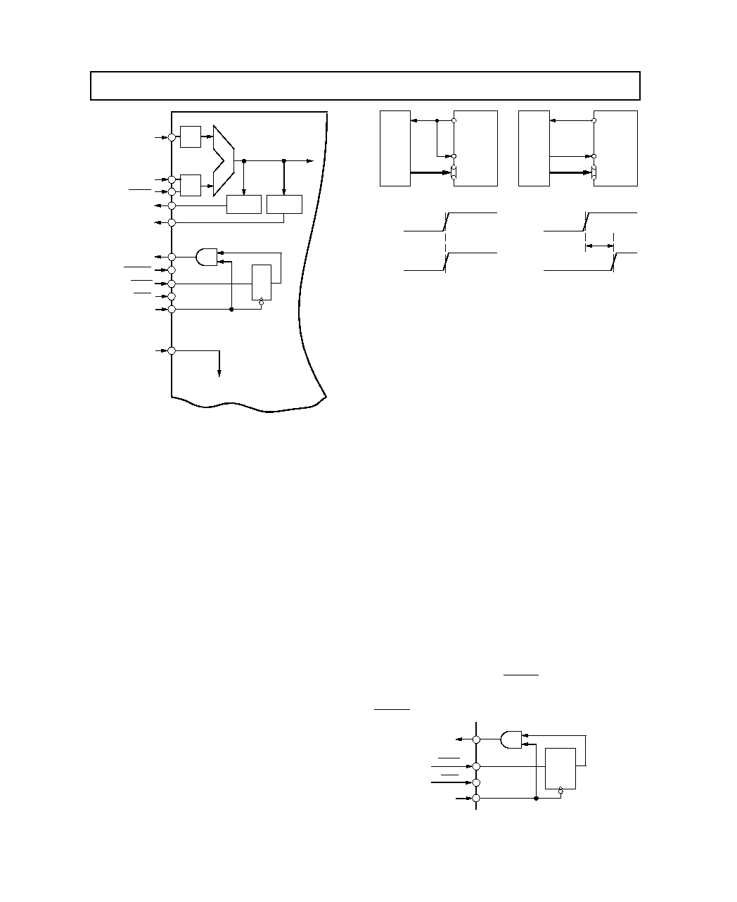
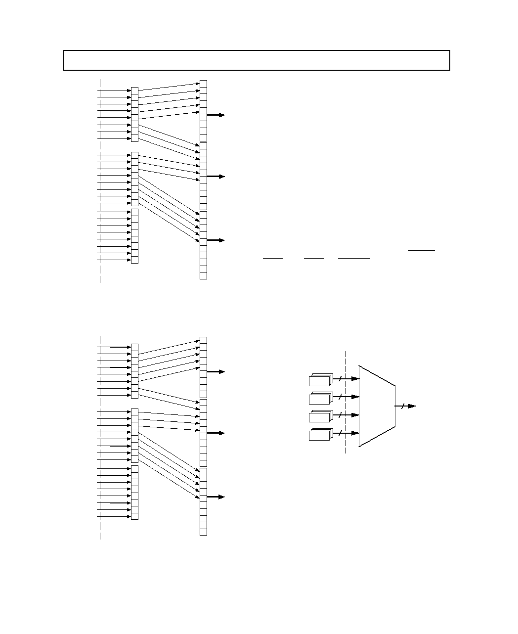
CLOCK CONTROL CIRCUIT
The ADV7160/ADV7162 has an integrated Clock Control Cir-
cuit (Figure 16). This circuit is capable of both generating the
ADV7160/ADV7162's internal clocking signals as well as exter-
nal graphics subsystem clocking signals. Total system synchro-
nization can be attained by using the parts output clocking
signals to drive the controlling graphics processor's master clock
as well as the video frame buffers shift clock signals.
CLOCK, CLOCK Inputs
The Clock Control Circuit is driven by the pixel clock inputs,
CLOCK and CLOCK. These inputs can be driven by a differ-
ential ECL oscillator running from a +5 V supply.
ADV7160/ADV7162
REV. 0
17
ADV7160/
ADV7162
LOADOUT
LOADIN
BLANK
SCKOUT
SCKIN
LATCH
EN
CLOCK
CLOCK
ECL
TO
TTL
DIVIDE BY
M (
÷
M)
DIVIDE BY
N (
÷
N)
PRGCKOUT
S
E
L
E
C
T
PLLREF
TO COLOR DATA
MULTIPLEXER
TRISYNC
PLL
SYNC
M IS A FUNCTION OF MULTIPLEX RATE
M = 8 IN 8:1 MULTIPLEX MODE
M = 4 IN 4:1 MULTIPLEX MODE
M = 2 IN 2:1 MULTIPLEX MODE
N IS INDEPENDENTLY PROGRAMMABLE
N = (4, 8, 16, 32)
Figure 16. Clock Control Circuit of the ADV7160/ADV7162
CLOCK CONTROL SIGNALS
LOADOUT
The ADV7160/ADV7162 generates a LOADOUT control sig-
nal which runs at a divided down frequency of the pixel
CLOCK. The frequency is automatically set to the pro-
grammed multiplex rate, controlled by CR37 and CR36 of
Command Register 3.
f
LOADOUT
= f
CLOCK
/8
8:1 multiplex mode
f
LOADOUT
= f
CLOCK
/4
4:1 multiplex mode
f
LOADOUT
= f
CLOCK
/2
2:1 multiplex mode
The LOADOUT signal is used to directly drive the LOADIN
pixel latch signal of the ADV7160/ADV7162. This is most sim-
ply achieved by tying the LOADOUT and LOADIN pins to-
gether. Alternatively, the LOADOUT signal can be used to
drive the frame buffer's shift clock signals, returning to the
LOADIN input delayed with respect to LOADOUT.
If it is not necessary to have a known fixed number of pipeline
delays, then there is no limitation on the delay between
LOADOUT and LOADIN (LOADOUT(1) and
LOADOUT(2)). LOADIN and Pixel Data must conform to
the setup and hold times (t
8
and t
9
).
If however, it is required that the ADV7160/ADV7162 has
a fixed number of pipeline delays (t
PD
) LOADOUT and
LOADIN must conform to timing specifications t
10
and
t
11
as
illustrated in Figures 5 to 10.
ADV7160/
ADV7162
LOADOUT
LOADIN
PIXEL
DATA
VIDEO
FRAME
BUFFER
LOADOUT(1)
LOADOUT(2)
ADV7160/
ADV7162
LOADOUT
LOADIN
PIXEL
DATA
VIDEO
FRAME
BUFFER
LOADOUT
LOADIN
LOADOUT(1)
LOADOUT(2)
DELAY
Figure 17. LOADOOUT vs Pixel Clock
Pipeline Delay and Onboard Calibration
The ADV7160/ADV7162 has a fixed number of pipeline delays
(t
PD
), so long as timings t
10
and
t
11
are met. However, if a
fixed number of pipeline delays is not a requirement, timings t
10
and
t
11
can be ignored, a calibration cycle must be run and
there is no restriction on LOADIN to LOADOUT timing. If
timings t
10
and
t
11
are not met, the part will function correctly
though with an increased number of pipeline delays. The
ADV7160/ADV7162 has on-board calibration circuitry which
synchronizes pixel data and LOADIN with the internal
ADV7160/ADV7162 clocking signals. Calibration can be per-
formed in two ways. During the device's initialization sequence
by toggling two bits of the Mode Register, MR10 followed by
MR15 or by writing a "1" to Bit CR10 of Command Register 1
and a "0" to MR15 which executes a calibration on every
Vertical Sync.
PRGCKOUT
The PRGCKOUT control signal outputs a user programmable
clock frequency. It is a divided down frequency of the pixel
CLOCK (see Figure 11). The rising edge of PRGCKOUT is
synchronous to the rising edge of LOADOUT.
f
PRGCKOUT
= f
CLOCK
/N
where N = 4, 8, 16 or 32.
One application of the PRGCKOUT is to use it as the master
clock frequency of the graphics subsystems processor or
controller.
SCKIN, SCKOUT
These video memory signals are used to minimize external sup-
port chips. Figure 18 illustrates the function that is provided.
An input signal applied to SCKIN is synchronously AND-ed
with the video blanking signal (BLANK). The resulting signal
is output on SCKOUT. Figure 12 of the Timing Waveform
section shows the relationship between SCKOUT, SCKIN and
BLANK
.
BLANK
SCKOUT
SCKIN
LATCH
ENABLE
SYNC
Figure 18. SCKOUT Generation Circuit
REV. 0
18
ADV7160/ADV7162
The SCKOUT signal is essentially the video memory shift con-
trol signal. It is stopped during the screen retrace. Figure 19 shows a
suggested frame buffer to ADV7160/ADV7162 interface. This is a
minimum chip solution and allows the ADV7160/ADV7162 con-
trol the overall graphics system clocking and synchronization.
LOADOUT
SCKOUT
ADV7160/
ADV7162
PIXEL
DATA
LOADIN
SCKIN
BLANK
VIDEO FRAME
BUFFER
Figure 19. ADV7160/ADV7162 Interface Using SCKIN
and SCKOUT
PLL
The on-board PLL can be used as an alternative clock source.
This eliminates the need for an external high speed clock gen-
erator such as a crystal oscillator. With the PLL, it is possible to
generate an internal clock whose frequency is a multiple of the PLL
reference frequency (PLL
REF
). Internal PLL operation is selected
by setting CR56 of Command Register 5 to Logic "1." The PLL
registers can be programmed to set up the frequency required.
The block diagram of the Phase Locked Loop is shown in Fig-
ure 20. The blocks consist of a phase frequency detector, a
charge pump, a loop filter, a voltage controlled oscillator and a
programmable divider.
VOLTAGE
CONTROLLED
OSCILLATOR
CHARGE
PUMP
PHASE
DETECTOR
REFERENCE
DIVIDER
PLL
REF
F
PD
FEEDBACK
DIVIDER
F
VCO
O/P
DIVIDER
F
OUT
F
PD
Figure 20. PLL Block Diagram
The phase frequency detector drives the voltage controlled oscil-
lator (VCO), to a frequency that will cause the two inputs to the
phase frequency detector to be matched in frequency and phase.
The corresponding output of the VCO can be calculated as:
VCO = PLL
REF
Feedback Divider
Reference Divider
The Reference Divider is set by a combination of the contents of
the PLL R Register and the RSEL bit. The PLL R Register has
a resolution of 7 bits. It is programmed by setting the PLL R
Register located at Control Register address 00CH . The PLL
R Register can be set from 01H to 7FH. It should not be set to
00H. If this register contains 00H, then the PLL stops. There-
fore, the Reference Divider can be set from 3 to 129 in steps of
one, or from 130 to 258 in steps of two by setting the RSEL bit.
The RSEL bit is accessed by changing Bit PCR1 of the PLL
Control Register. The Feedback Divider is set by a combina-
tion of the contents of the PLL V Register, the VSEL bit and
the S value. The S value is set up in PCR7 and PCR6 of the
PLL Command Register. This S value allows a better resolu-
tion when setting the Feedback Divider value. The PLL V Reg-
ister has a resolution of 7 bits. It is programmed by setting the
PLL V Register located at Control Register address 00FH .The
PLL V Register can be set from 01H to 7FH. It should not be
set to 00H. If this register contains 00H, then the PLL stops.
Therefore the feedback divider can be set from 12 to 519 in
steps of one, or from 520 to 1038 in steps of two by setting the
VSEL bit. The VSEL bit is accessed by changing bit PCR2 of
the PLL Control Register. The P counter divides the output
from the oscillator by 1, 2, 4 or 8 as determined by PSEL1 and
PSEL0 which are set in bits PCR5 and PCR4 of the PLL Con-
trol Register. This post-scaler is useful in the generation of
lower frequencies as the VCO has been optimized for high
frequency operation.
(1 +
VSEL
)(4(V+2) + S)
(1 + RSEL)(R+2)
PLL
REF
F
VCO
VCO
VCO/2
VCO/4
VCO/8
PSEL1 PSEL0
F
OUT
F
OUT
F
VCO
F
VCO
/2
F
VCO/
4
F
VCO/
8
PSEL1
0
0
1
1
PSEL0
0
1
0
1
Figure 21. PLL Transfer Function
The transfer function of the PLL can be summarized by the
block diagram shown in Figure 21.
To optimize the performance of the on-board PLL, the follow-
ing criteria should be followed:
900 kHz
< PLL
REF
< 40 MHz
300 kHz
< F
PD
< 10 MHz
120 MHz
< F
VCO
< 260 MHz
For F
VCO
> 220 MHz, V
SEL
should be programmed to logic "0."
Any lower frequency output can be achieved by using the output
divider.
A jitter performance graph as a function of both F
PD
and F
VCO
is
illustrated in Figure 22. It can be seen that jitter decreases with
increasing F
VCO
and also that jitter decreases with increasing
F
PD
. For each F
OUT
, the user should firstly maximize F
VCO
us-
ing the output divider and then pick PLL
REF
and reference di-
vide to maximize FPD. When generating multiple output
frequencies from one PLL
REF
value, an iterative process should
be used to find the PLL
REF
value that gives the best trade off be-
tween jitter performance and F
OUT
accuracy.
VCO FREQUENCY MHz
250
0
50
300
100
150
200
250
200
150
100
50
FPD = 0.3MHz
FPD = 0.42MHz
FPD = 0.57MHz
FPD = 0.8MHz
FPD = 1.0MHz
FPD = 1.5MHz
FPD = 2.0MHz
FPD = 2.7MHz
FPD = 4.0MHz
FPD = 5.3MHz
JITTER MEASURED AT 15µs
RMS JITTER ps
Figure 22. PLL Jitter
ADV7160/ADV7162
REV. 0
19
COLOR VIDEO MODES
The ADV7160/ADV7162 supports a number of color video
modes all at the maximum video rate.
Command bits CR27CR24 of Command Register 2 along with
bit MR11 of Mode Register 1 determine the color mode. Seven
color modes use the Color Palette, and three of them bypass the
palette and control the DACs directly.
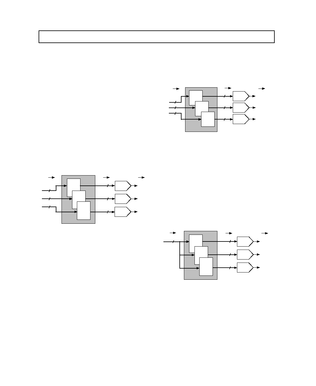
24-Bit True Color
(CR27, CR26, CR25, CR24 = 1, 1, 1, 0)
The part is set to 24-bit/30-bit "Gamma" True-Color operation
with MR11 set to Logic "1" and direct 24-bit True-Color op-
eration with MR11 set to Logic "0." The pixel port accepts 24
bits of color data which is directly mapped to the Look-Up
Table RAM. With MR11 set to Logic "1," the Look-Up Table
is configured as a 256 location by 30 bits deep RAM (10 bits
each for Red, Green and Blue), the RAM is preloaded with a
user determined, nonlinear function, such as a gamma correc-
tion curve and the output of the RAM drives the DACs with
30-bit data. With MR11 set to Logic "0," the Look-Up Table is
configured as a 256 location by 24 bits deep RAM (8 bits each
for Red, Green and Blue), the RAM is preloaded with a linear
function and the output of the RAM drives the DACs with 24-
bit data.
8
8
8
24-BIT COLOR
DATA
24-BIT TO 30-BIT
LOOK-UP TABLE
30-BIT COLOR
DATA
ANALOG VIDEO
OUTPUTS
RED
256 x 10
10
10
10
10-BIT
RED
DAC
10-BIT
GREEN
DAC
10-BIT
BLUE
DAC
RED
OUT
GREEN
OUT
BLUE
OUT
GREEN
256 x 10
BLUE
256 x 10
Figure 23. 24-Bit to 30-Bit True-Color Configuration
16-Bit True Color
(CR27, CR26, CR25, CR24 = 1, 0, 1, 1)
The part is set to 16-bit True-Color operation. The pixel port
accepts 16 bits of color data which is mapped to the 5 LSBs of
each of the red and blue palettes of the Look-Up-Table RAM,
and 6 LSBs of the green palette of the Look-Up-Table RAM.
With MR11 set to Logic "1," the Look-Up Table is configured
as a 64 location by 30 bits deep RAM (10 bits each for Red,
Green and Blue) and the output of the RAM drives the DACs
with 30-Bit data, allowing the display of 16-bit Gamma-
Corrected True-Color Images. With MR11 set to Logic "0,"
the Look-Up Table is configured as a 64 location by 24 bits
deep RAM (8 bits each for Red, Green and Blue); and the out-
put of the RAM drives the DACs with 24-bit data, allowing the
display of 16-bit True-Color Images.
15-Bit True Color
(CR27, CR26, CR25, CR24 = 1, 1, 0, 0 or 1, 1, 0, 1)
The part is set to 15-bit True-Color operation. The pixel port
accepts 15 bits of color data which is mapped to the 5 LSBs of
each of the red, green and blue palettes of the Look-Up Table
RAM. With MR11 set to Logic "1," the Look-Up Table is con-
figured as a 32 location by 30 bits deep RAM (10 bits each for
Red, Green and Blue) and the output of the RAM drives the
DACs with 30-bit data, allowing the display of 15-bit Gamma-
Corrected True-Color Images. With MR11 set to Logic "0,"
the Look-Up Table is configured as a 32 location by 24 bits
deep RAM (8 bits each for Red, Green and Blue) and the out-
put of the RAM drives the DACs with 24-bit data, allowing the
display of 15-bit True-Color Images.
15-BIT COLOR
DATA
15-BIT TO 24-BIT
LOOK-UP TABLE
ANALOG VIDEO
OUTPUTS
RED
32 x 8
GREEN
32 x 8
BLUE
32 x 8
5
5
5
8
8
8
8-BIT
RED
DAC
8-BIT
GREEN
DAC
8-BIT
BLUE
DAC
RED
OUT
GREEN
OUT
BLUE
OUT
24-BIT COLOR
DATA
Figure 24. 15-Bit to 24-Bit True-Color Configuration
8-Bit Pseudo Color
(CR27, CR26, CR25, CR24 = 0, 0, 0, 0 or 0, 1, 0, 0 or 1, 0, 0, 0)
This mode sets the part into 8-bit Pseudo-Color operation. The
pixel port accepts 8 bits of pixel data, from either the red, blue
or green channel. With MR11 set to Logic "1," a 30-bit word is
indexed in the Look-Up Table RAM. The Look-Up Table is
configured as a 256 location by 30 bits deep RAM (10 bits each
for Red, Green and Blue). The output of the RAM drives the
DACs with 30-bit data. With MR11 set to Logic "0," a 24-Bit
word is indexed in the Look-Up Table RAM. The Look-Up
Table is configured as a 256 location by 24 bits deep RAM (8
bits each for Red, Green and Blue). The output of the RAM
drives the DACs with 24-bit data. This mode allows for the dis-
play of 256 simultaneous colors out of a total palette of millions
of addressable colors.
8-BIT PIXEL
DATA
8-BIT TO 30-BIT
LOOK-UP TABLE
30-BIT COLOR
DATA
ANALOG VIDEO
OUTPUTS
RED
256 x 10
10
10
10
10-BIT
RED
DAC
10-BIT
GREEN
DAC
10-BIT
BLUE
DAC
RED
OUT
GREEN
OUT
BLUE
OUT
8
GREEN
256 x 10
BLUE
256 x 10
Figure 25. 8-Bit to 30-Bit Pseudo-Color Configuration
PIXEL PORT MAPPING
The pixel data to the ADV7160/ADV7162 is automatically
mapped in the parts pixel port as determined by the pixel data
mode programmed (Bits CR27CR24 of Command Register 2).
Pixel data in the 24-bit True-Color modes is directly mapped to
the 24 color inputs R7R0, G7G0 and B7B0.
There is one mode of operation for 16-bit True Color. Data is
input to the device over the red and green color ports (R7R0
and G7G0) and is internally mapped to LUT Locations 063
according to Figure 26. (Note: Data on unused pixel inputs is
ignored.)
.
REV. 0
20
ADV7160/ADV7162
TO
BLUE
DAC
TO
GREEN
DAC
TO
RED
DAC
10
10
10
0
R4
R3
R2
R1
R0
0
0
R7
R4
R3
R2
R1
R0
R6
R5
0
G4
G3
G2
G1
G0
0
G5
G7
G4
G3
G2
G1
G0
G6
G5
0
B4
B3
B2
B1
B0
0
0
x
x
x
x
x
x
x
x
R7
R4
R3
R2
R1
R0
R6
R5
G7
G4
G3
G2
G1
G0
G6
G5
B7
B4
B3
B2
B1
B0
B6
B5
R4
R3
R2
R1
R0
G5
G4
G3
G2
G1
G0
B4
B3
B2
B1
B0
x
x
x
x
x
x
x
x
PIXEL
INPUT
DATA
PIN
ASSIGN-
MENTS
DATA
LATCHED
TO
PIXEL
PORT
DATA
INTERNALLY
SHIFTED
TO 5 OR 6 LSBs
DATA LATCHES
FIRST 32 OR 64
LOCATIONS
OF RAM
256 x 10 RAM
(RED LUT)
LOCATION
"31"
LOCATION
"0"
5
256 x 10 RAM
(GREEN LUT)
LOCATION
"63"
LOCATION
"0"
5
256 x 10 RAM
(BLUE LUT)
LOCATION
"31"
LOCATION
"0"
5
Figure 26. 16-Bit True-Color Mapping using R7R0
and G7G0
256 x 10 RAM
(RED LUT)
LOCATION
"31"
LOCATION
"0"
5
TO
BLUE
DAC
TO
GREEN
DAC
TO
RED
DAC
10
10
10
0
R4
R3
R2
R1
R0
0
0
x
R4
R3
R2
R1
R0
x
x
0
G4
G3
G2
G1
G0
0
0
0
B4
B3
B2
B1
B0
0
0
B4
B1
B0
x
x
x
B3
B2
R7
R4
R3
R2
R1
R0
R6
R5
G7
G4
G3
G2
G1
G0
G6
G5
B7
B4
B3
B2
B1
B0
B6
B5
R4
R3
R2
R1
R0
x
x
x
G4
G3
G2
G1
G0
x
x
x
B4
B3
B2
B1
B0
x
x
x
PIXEL
INPUT
DATA
PIN
ASSIGN-
MENTS
DATA
LATCHED
TO
PIXEL
PORT
DATA
INTERNALLY
SHIFTED
TO 5 LSBs
DATA LATCHES
FIRST 32
LOCATIONS
OF RAM
256 x 10 RAM
(GREEN LUT)
LOCATION
"31"
LOCATION
"0"
5
256 x 10 RAM
(BLUE LUT)
LOCATION
"31"
LOCATION
"0"
5
x
G4
G3
G2
G1
G0
x
x
Figure 27. 15-Bit True Color Mapping using R7R3, G7G3
and B7B3
TO
BLUE
DAC
TO
GREEN
DAC
TO
RED
DAC
10
10
10
0
R4
R3
R2
R1
R0
0
0
x
R4
R3
R2
R1
R0
R6
R5
0
G4
G3
G2
G1
G0
0
0
G7
G4
G3
G2
G1
G0
G6
G5
0
B4
B3
B2
B1
B0
0
0
x
x
x
x
x
x
x
x
R7
R4
R3
R2
R1
R0
R6
R5
G7
G4
G3
G2
G1
G0
G6
G5
B7
B4
B3
B2
B1
B0
B6
B5
x
R4
R3
R2
R1
R0
G4
G3
G2
G1
G0
B4
B3
B2
B1
B0
x
x
x
x
x
x
x
x
PIXEL
INPUT
DATA
PIN
ASSIGN-
MENTS
DATA
LATCHED
TO
PIXEL
PORT
DATA
INTERNALLY
SHIFTED
TO 5 LSBs
DATA LATCHES
FIRST 32
LOCATIONS
OF RAM
256 x 10 RAM
(RED LUT)
LOCATION
"31"
LOCATION
"0"
5
256 x 10 RAM
(GREEN LUT)
LOCATION
"31"
LOCATION
"0"
5
256 x 10 RAM
(BLUE LUT)
LOCATION
"31"
LOCATION
"0"
5
Figure 28. 15-Bit True-Color Mapping using R6R0
and G7G0
The part has two modes of operation for 15-bit True Color. In
the first mode, data is input to the device over the red, green
and blue channel (R7R3, G7G3 and B7B3) and is internally
mapped to Locations 0 to 31 of the Look-Up Table (LUT)
according to Figure 27.
In the second mode, data is input to the device over just two of
the color ports, red and green (R7R0 and G7G0) and is inter-
nally mapped to LUT Locations 0 to 31 according to Figure 30.
(Note: Data on unused pixel inputs is ignored.)
There are three modes of operation for 8-bit Pseudo Color.
Each mode maps the input pixel data differently. Data can be
input into one of the three color channels, R7R0 or G7G0 or
B7B0.
In 24-bit Palette Bypass Mode, the red, blue and green color
channels bypass the Pixel Mask and the Color Palette. Each 8-
bit color channel is mapped onto the 8 MSBs of the correspond-
ing 10-bit DAC input. The two LSBs on each DAC are zeros.
The Bypass Mode can be selected in two ways, by using CR27
CR24 of Command Register 2 or on a pixel by pixel basis using
the PS inputs (ADV7160 only).
In 16-bit Palette Bypass Mode, the color channels bypass the
Pixel Mask and the Color Palette. The 8-bits of red pixel data
and 8-bits of green pixel data are mapped onto the 5 MSBs of
the red and blue DAC input and the 6 MSBs of the green DAC
input as shown in Figure 29. The remaining LSBs on each
DAC are zeros. The Bypass Mode can be selected in two ways,
by using CR27CR24 of Command Register 2 or on a pixel by
pixel basis using the PS inputs (ADV7160 only).
ADV7160/ADV7162
REV. 0
21
R6
R3
R2
R1
R0
G7
R5
R4
G7
G4
G3
G2
G1
G0
G6
G5
x
x
x
x
x
x
x
x
R8
R5
0
0
0
0
R7
R6
R9
G8
G5
G4
0
0
0
G7
G6
G9
0
B8
B5
0
0
0
0
B7
B6
B9
0
R7
R4
R3
R2
R1
R0
R6
R5
G7
G4
G3
G2
G1
G0
G6
G5
B7
B4
B3
B2
B1
B0
B6
B5
R9
R8
R7
R6
R5
G9
G8
G7
x
G6
G5
B9
B8
B7
B6
B5
x
x
x
x
x
x
x
x
PIXEL
INPUT
DATA
PIN
ASSIGN-
MENTS
DATA
LATCHED
TO
PIXEL PORT
DATA LATCHED
TO DAC INPUTS
IOR
IOG
IOB
RED
DAC
GREEN
DAC
BLUE
DAC
Figure 29. 16-Bit True-Color in Bypass Mode using R7R0
and G7G0
x
R4
R3
R2
R1
R0
R6
R5
G7
G4
G3
G2
G1
G0
G6
G5
x
x
x
x
x
x
x
x
R8
R5
0
0
0
0
R7
R6
R9
G8
G5
0
0
0
0
G7
G6
G9
0
B8
B5
0
0
0
0
B7
B6
B9
0
R7
R4
R3
R2
R1
R0
R6
R5
G7
G4
G3
G2
G1
G0
G6
G5
B7
B4
B3
B2
B1
B0
B6
B5
G7
G6
G5
B9
B8
B7
B6
B5
x
x
x
x
x
x
x
x
PIXEL
INPUT
DATA
PIN
ASSIGN-
MENTS
DATA
LATCHED
TO
PIXEL PORT
DATA LATCHED
TO DAC INPUTS
IOR
IOG
IOB
RED
DAC
GREEN
DAC
BLUE
DAC
x
R9
R8
R7
R6
R5
G9
G8
Fiigure 30. 15-Bit True-Color in Bypass Mode using R6R0
and G7G0
In 15-bit Palette Bypass Mode, the color channels bypass the
Pixel Mask and the Color Palette. The 7 bits of red pixel data
and 8 bits of green pixel data are mapped onto the 5 MSBs of
the red, green and blue DAC input as shown in Figure 30. The
remaining LSBs on each DAC are zeros. The Bypass Mode can
be selected in two ways, by using CR27CR24 of Command
Register 2 or on a pixel by pixel basis using the PS inputs
(ADV7160 only).
Multiplexing
The on-board multiplexers of the ADV7160/ADV7162 elimi-
nate the need for external data serializer circuits. Multiple video
memory devices can be connected, in parallel, directly to the de-
vice. Figure 31 shows four memory banks of 50 MHz memory
connected to the ADV7160, running in 4:1 multiplex mode,
giving a resultant pixel or dot clock rate of 200 MHz. Instead of
having to provide a new pixel at the input every 5 ns, four pixels
are provided together every 20 ns. The input multiplexer takes
the four pixels latched in parallel, and selects them one at a time
to produce a pixel stream at the pixel clock rate. In 4:1 mode,
the pixels are selected in the sequence A, B, C, D, cycling continu-
ously. In 2:1 mode, the A and B pixels are selected. The 8:1
mode is only available in 8-bit Pseudo-Color Mode. BLANK,
SYNC
, ODD/EVEN and TRISYNC are not multiplexed and
can only change on a 1, 2, 4 or 8 pixel boundary depending on
the multiplex mode.
On the rising edge of LOADIN, all the pixel port inputs are
latched into the ADV7160/ADV7162. The LOADIN frequency
must be a divided down frequency of the pixel clock frequency.
This can be achieved using LOADOUT to directly drive
LOADIN as LOADOUT provides the correct frequency re-
quired, or drive LOADIN after delay through some external cir-
cuitry.
MULTIPLEXER
50MHz
50MHz
50MHz
50MHz
50MHz
50MHz
50MHz
50MHz
50MHz
50MHz
50MHz
50MHz
24
24
24
24
24
200MHz
(4
×
50MHz)
VIDEO MEMORY/
FRAME BUFFER
ADV7160/ADV7162
VRAM (BANK A)
VRAM (BANK B)
VRAM (BANK C)
VRAM (BANK D)
Figure 31. Direct Interfacing of Video Memory to
ADV7160/ADV7162
8-Bit Pseudo Color in 8:1 Multiplexing Mode
When 8:1 Multiplexing Mode is selected by setting Bit CR37 of
Command Register 3 to Logic "1" and bit CR36 of Command
Register 3 to Logic "0," the ADV7160/ADV7162 goes into 8-
Bit Pseudo-Color Mode irrespective of the Color Mode selected
by Bits CR27 to CR24 in Command Register 2. Hence
LOADOUT operates at f
CLOCK
/8. Eight 8-bit pixels are latched
in parallel by the rising edge of LOADIN. These 8-bit pixels
are then selected, one at a time, to produce an 8-bit pixel stream
which passes through the Pixel Mask to address the LUT. The
order the eight 8-bit pixels are displayed is GA, RA, GB, RB,
GC, RC, GD, RD.
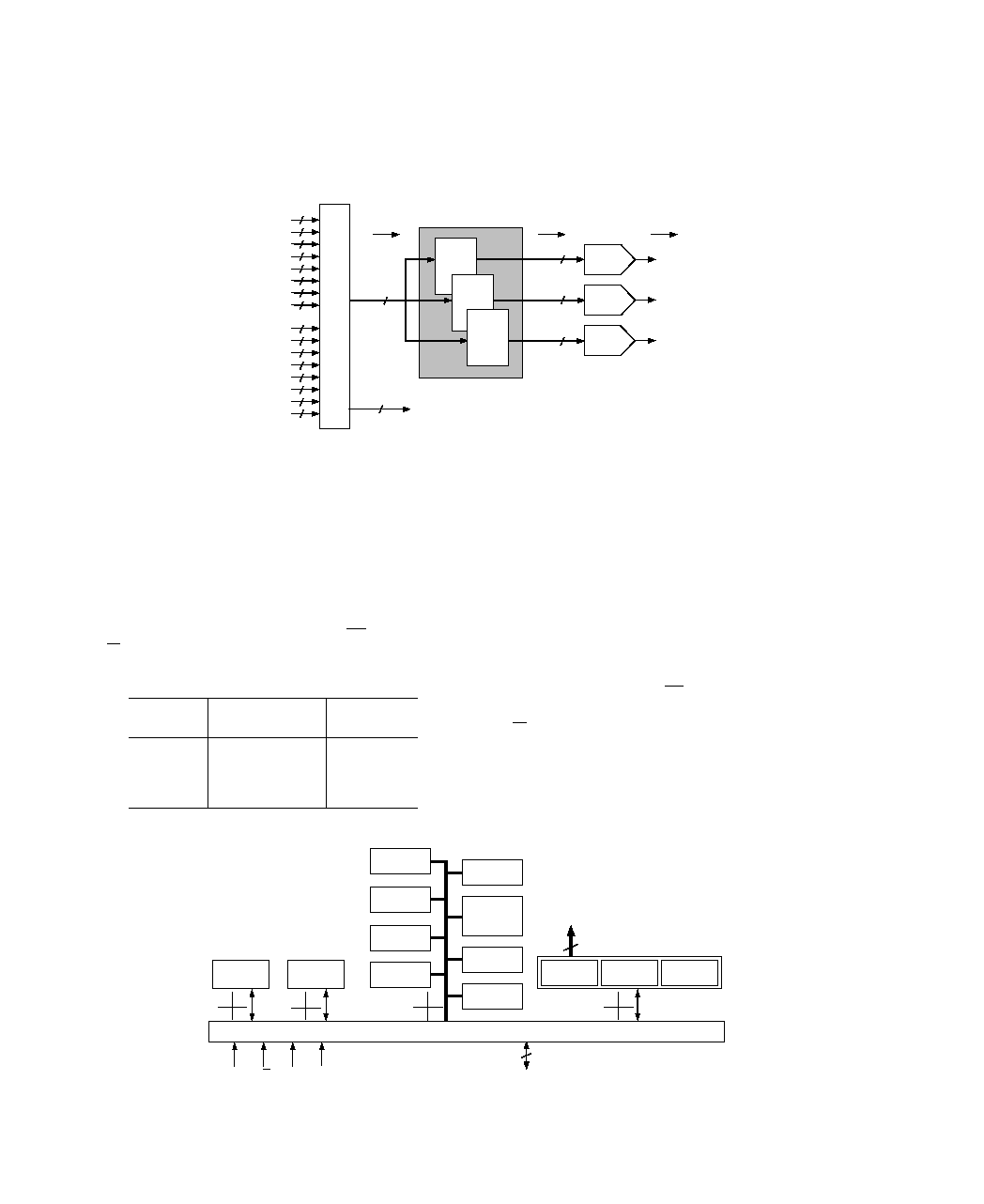
REV. 0
22
ADV7160/ADV7162
Figure 33. MPU Port and Register Configuration
MICROPROCESSOR (MPU PORT)
The ADV7160/ADV7162 supports a standard MPU Interface.
All the functions of the part are controlled via this MPU port.
Direct access is gained to the Address Register, Mode Register
and all the Control Registers as well as the Color Palette. The
following sections describe the setup for reading and writing to
all of the devices registers.
MPU Interface
The MPU interface (Figure 33) consists of a bidirectional, 10-
bit wide databus and interface control signals CE, C0, C1 and
R/W. The 10-bit wide databus is user configurable as illustrated.
Table I. Data-Bus Width
Data-Bus
RAM/DAC
Read/Write
Width
Resolution
Mode
10-Bit
10-Bit
10-Bit Parallel
10-Bit
8-Bit
8-Bit Parallel
8-Bit
10-Bit
8 + 2 Byte
8-Bit
8-Bit
8-Bit Parallel
Register Mapping
The ADV7160/ADV7162 contains a number of on-board regis-
ters including the Mode Register (MR17MR10), Address Reg-
ister (A10A0) and many Control Registers as well as Color
Palette Registers. These registers control the entire operation of
the part. Figure 34 shows the internal register configuration.
Control lines C1 and C0 determine which register the MPU is
accessing. C1 and C0 also determine whether the Address Reg-
ister is pointing to the color registers and Look-Up Table RAM
or the control registers. If C1, C0 = 1, 0 the MPU has access to
whatever control register is pointed to by the Address Register
(A10A0). If C1, C0 = 0, 1 the MPU has access to the Look-
Up Table RAM (Color Palette) or the Overlay Palette through
the associated color registers. The CE input latches data to or
from the part.
The R/W control input determines between read or write ac-
cesses. The truth tables show all modes of access to the various
registers and color palette for both the 8-bit wide databus con-
figuration and 10-bit wide data bus configuration. It should be
noted that after power-up, the devices MPU port is automati-
cally set to 10-bit wide operation (see Power-On Reset section).
Figure 32. 8-Bit Pseudo Color in 8:1 Multiplexing Mode
The unused Blue pixel inputs are used, in this mode, to provide
8 extra PS inputs. These PS inputs provide 2 bits after 8:1 mul-
tiplexing. The PS inputs can be used as Overlay or Palette Se-
lect inputs.
2
PS
P
I
X
E
L
I
N
P
U
T
M
U
L
T
I
P
L
E
X
E
R
G7G0
R7R0
G7G0
R7R0
G7G0
R7R0
G7G0
R7R0
PS1PS0
B1B0
PS1PS0
B1B0
PS1PS0
B1B0
PS1PS0
B1B0
A
B
C
D
E
F
G
H
A
B
C
D
E
F
G
H
8
8
8
8
8
8
8
8
8
8
8
8
8
8
8
8
8-BIT COLOR
DATA
24-BIT TO 30-BIT
LOOK-UP-TABLE
30-BIT COLOR
DATA
ANALOG VIDEO
OUTPUTS
RED
256 x 10
10
10
10
10-BIT
RED
DAC
10-BIT
GREEN
DAC
10-BIT
BLUE
DAC
RED
OUT
GREEN
OUT
BLUE
OUT
8
GREEN
256 x 10
BLUE
256 x 10
MPU PORT
C0
CE
R/W
10 (8+2)
RED
REGISTER
DATA TO
PALETTES
30
CURSOR
REGISTERS
TEST
REGISTERS
ID
REGISTER
STATUS
REGISTER
PIXEL MASK
REGISTER
REVISION
REGISTER
PLL
REGISTERS
COMMAND
REGISTERS
(CR1CR5)
C1
D9D0
ADDRESS
REGISTER
MODE
REGISTER
GREEN
REGISTER
BLUE
REGISTER
CONTROL REGISTERS
COLOR REGISTERS
C1 C0
1 1
ADDR
(A10-A0)
(MRI)
C1 C0
0 1
C1 C0
0 0
C1 C0
1 0
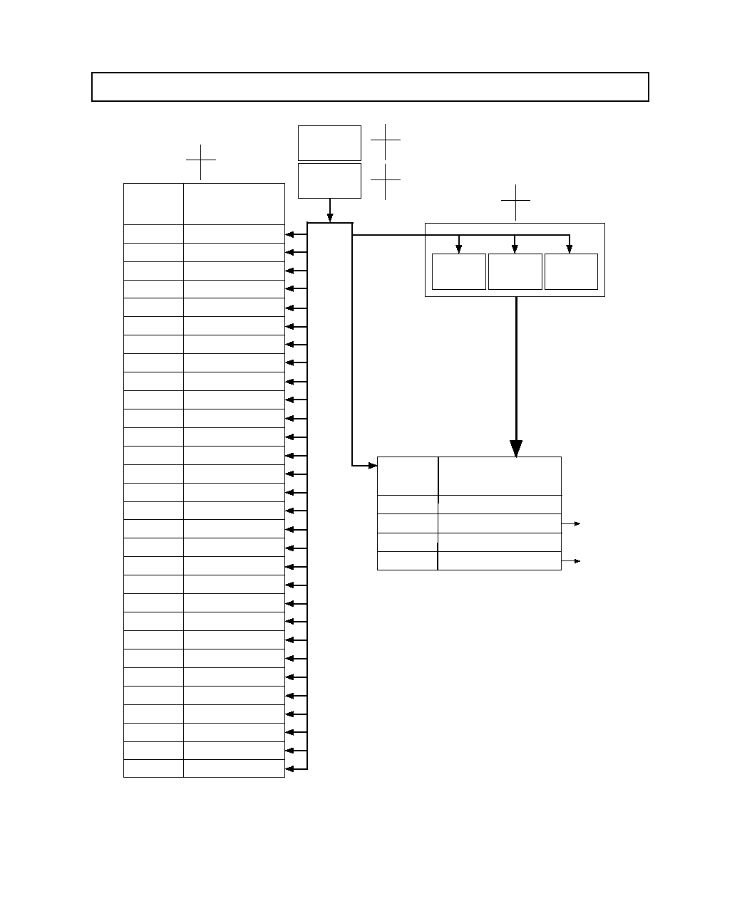
ADV7160/ADV7162
REV. 0
23
Figure 34. Internal Register Configuration and Address Decoding
MODE
REGISTER
(MR17MR10)
ADDRESS
REGISTER
(A10A0)
C1 C0
1 1
C1 C0
0 0
RED
REGISTER
(R9-R0)
GREEN
REGISTER
(G9-G0)
BLUE
REGISTER
(B9-B0)
C1 C0
0 1
POINTS TO LOCATION
CORRESPONDING TO
ADDRESS REGISTER
(A10A0)
COLOR PALETTE
7FFH 104H
103H 101H
100H
0FFH 000H
RESERVED
OVERLAY COLOR 13 (3 x 30)
RESERVED
LOOK-UP TABLE RAM (256 x 30)
ADDRESS REG
= ADDRESS
REG +1
ADDRESS
REGISTER
(A10A0)
CURSOR IMAGE
RESERVED
CURSOR COLOR 1
CURSOR COLOR 2
RESERVED
CURSOR CONTROL REG
CURSOR Y-HI REG
CURSOR Y-LO REG
CURSOR X-HI REG
CURSOR X-LO REG
RESERVED
TEST REGISTER
SIGNATURE MISC REG
SIGNATURE BLUE REG
SIGNATURE GREEN REG
SIGNATURE RED REG
PLL V REG
TEST REG
COMMAND REG 5
PLL R REG
REVISION REG 001H
STATUS REG
PLL COMMAND REG
COMMAND REG 4
COMMAND REG 3
COMMAND REG 2
COMMAND REG 1
PIXEL MASK REG
ID REG
TEST REGISTERS
CONTROL
REGISTERS
C1 C0
1 0
ADDRESS
REGISTER
(A10A0)
7FFH 400H
3FFH 305H
304H
303H
302H 205H
204H
203H
202H
201H
200H
1FFH 016H
015H 014H
013H
012H
011H
010H
00FH
00EH
00DH
00CH
00BH
00AH
009H
008H
007H
006H
005H
004H
003H
002H 000H
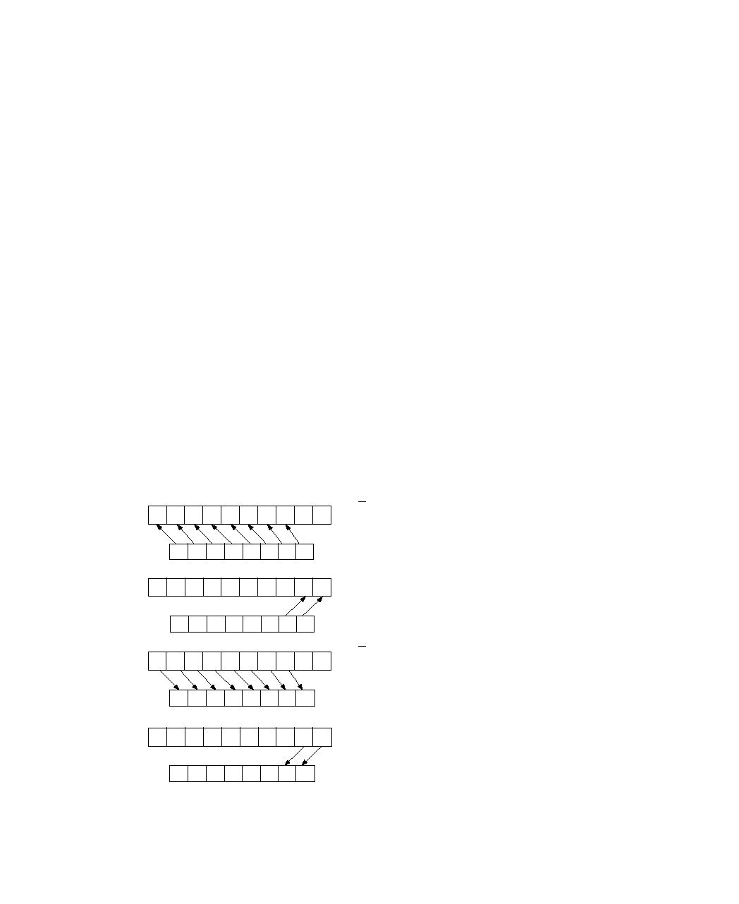
REV. 0
24
ADV7160/ADV7162
Power-On Reset
On power-up, the ADV7160/ADV7162 executes a power-on re-
set operation. This initializes the pixel port such that the pixel
sequence ABCD starts at A. The Mode Register (MR17MR10),
Command Register 2 (CR27CR20), Command Register 3
(CR37CR30) have all bits set to a Logic "1" and Address Reg-
ister, Command Register 1 (CR17CR10), Command Register 4
(CR47CR40) and Command Register 5 (CR57CR50) have
all bits set to a Logic "0."
The output clocking signals are also set during this reset period.
PRGCKOUT = CLOCK/32
LOADOUT
= CLOCK/4:
The power-on reset is activated when V
AA
goes from 0 V to 5 V
This reset is active for 1
µ
s. The ADV7160/ADV7162 should
not be accessed during this reset period. The pixel clock should
be applied at power-up.
Color Palette Accesses
The Color Palette consists of 256 RAM locations, each location
containing 30 bits of color information. Data is written to the
color palette by firstly writing to the address register of the color
palette location to be modified. The MPU performs three suc-
cessive write cycles for each of the red, green and blue registers
(10-bit or 8-bit). Figures 35 to 38 illustrate write operations for
a 10-bit databus using the DACs in 8-bit and 10-bit mode and
write operations for an 8-bit databus using the DACs in 8-bit
and 10-bit mode. An internal pointer moves from red to green
to blue after each write is completed. This pointer is reset to
red after a blue write or whenever the address register is written.
During the blue write cycle, the three bytes of red, green and
blue are concatenated into a single 30-bit/24-bit word and writ-
ten to the RAM location as specified in the address register
(A10A0).
The address register then automatically increments to point to
the next RAM location and a similar red, green and blue palette
write sequence is performed. The address register resets to
000H following a blue write cycle to color palette RAM location
0FFH. The three color overlay palette is located in address
space above the main color palette. To access the Overlay
Palette, the Address Register must first be written with address
101H. From then on, the colors are accessed in the same way
as the main Color Palette, with the Address Register incrementing
after each blue access.
Data is read from the Color Palette by firstly writing to the ad-
dress register of the color palette location to be read. The MPU
performs three successive read cycles from each of the red,
green and blue locations (10-bit or 8-bit) of the RAM. Figures
35 to 38 illustrate read operations for a 10-bit databus using the
DACs in 8-bit and 10-bit mode and read operations for an 8-bit
databus using the DACs in 8-bit and 10-bit mode. An internal
pointer moves from red to green to blue after each read is com-
pleted. This pointer is reset to red after a blue read or whenever
the address register is written. The address register then auto-
matically increments to point to the next RAM location and a
similar red, green and blue palette read sequence is performed.
The address register resets to 000H following a blue read cycle
of color palette RAM location 0FFH. Similarly for the Overlay
Palette, the Address Register must first be written with address
101H. From then on, the colors are read in the same way as the
main Color Palette, with the Address Register incrementing af-
ter each blue access.
Figure 35. 8-Bit Data Bus Using 10-Bit DACs
D7
D1
D2
D3
D4
D5
D6
D0
Databus
R9
R3
R4
R5
R6
R7
R8
R0
R1
R2
First Write Operation
Palette
R9
R3
R4
R5
R6
R7
R8
R0
R1
R2
Second Write Operation
Palette
D7
D1
D2
D3
D4
D5
D6
D0
R9
R3
R4
R5
R6
R7
R8
R0
R1
R2
First Read Operation
Palette
R9
R3
R4
R5
R6
R7
R8
R0
R1
R2
Second Read Operation
Palette
R/
W
C1
C0
Palette Write
0
0
0
Write to Address Register (Lo- Byte)
0
0
0
Write to Address Register (Hi- Byte)
0
0
1
Write Red Data (R9R2)
0
0
1
Write Red Data (R1R0)
0
0
1
Write Green Data (G9G2)
0
0
1
Write Green Data (G1G0)
0
0
1
Write Blue Data (B9B2)
0
0
1
Write Blue Data (B1B0)
0
0
1
Write Red Data (R9R2)
.
.
R/
W
C1
C0
Palette Read
0
0
0
Write to Address Register (Lo- Byte)
0
0
0
Write to Address Register (Hi- Byte)
1
0
1
Read Red Data (R9R2)
1
0
1
Read Red Data (R1R0)
1
0
1
Read Green Data (G9G2)
1
0
1
Read Green Data (G1G0)
1
0
1
Read Blue Data (B9B2)
1
0
1
Read Blue Data (B1B0)
1
0
1
Read Red Data (R9R2)
.
.
Databus
D7
D1
D2
D3
D4
D5
D6
D0
Databus
Databus
x
D1
x
x
x
x
x
D0
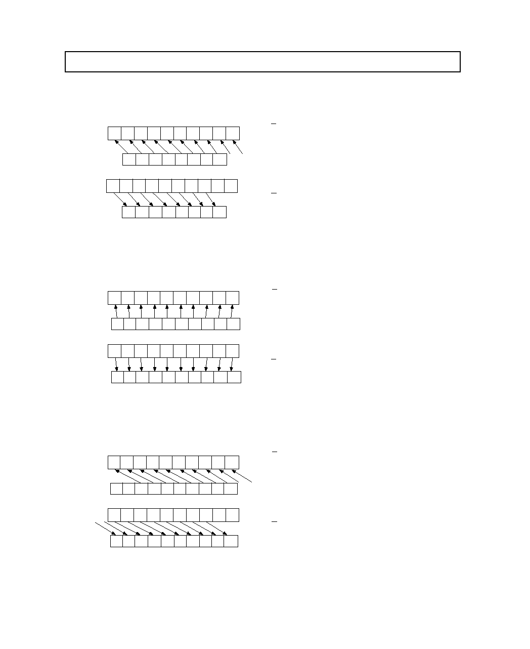
ADV7160/ADV7162
REV. 0
25
Register Accesses
The MPU can write to or read from all of the ADV7160/
ADV7162's registers. C0 and C1 determine whether the Mode
Register or Address Register is being accessed. Access to these
registers is direct. The Control Registers are accessed indi-
rectly. The Address Register must point to the desired Control
Register. Figure 33 and Figures 35 to 38 illustrate the structure
and protocol for device communication over the MPU port.
Databus
R9
R3
R4
R5
R6
R7
R8
R0
R1
R2
Write Operation
Palette
Databus
R9
R3
R4
R5
R6
R7
R8
R0
R1
R2
Read Operation
Palette
R/
W
C1
C0
Palette Write
0
0
0
Write to Address Register (Lo-Byte)
0
0
0
Write to Address Register (Hi-Byte)
0
0
1
Write Red Data (R9R0)
0
0
1
Write Green Data (G9G0)
0
0
1
Write Blue Data (B9B0)
0
0
1
Write Red Data (R9R0)
.
.
R/
W
C1
C0
Palette Read
0
0
0
Write to Address Register (Lo-Byte)
0
0
0
Write to Address Register (Hi-Byte)
1
0
1
Read Red Data (R9R0)
1
0
1
Read Green Data (G9G0)
1
0
1
Read Blue Data (B9B0)
1
0
1
Read Red Data (R9R0)
.
.
D2
D3
D4
D5
D6
D7
D0
D1
0
0
D2
D3
D4
D5
D6
D7
D0
D1
Figure 36. 8-Bit Databus Using 8-Bit DACs
Databus
R9
R3
R4
R5
R6
R7
R8
R0
R1
R2
Write Operation
Palette
R9
R3
R4
R5
R6
R7
R8
R0
R1
R2
Read Operation
Palette
D9
D3
D4
D5
D6
D7
D8
D0
D1
D2
Databus
D9
D3
D4
D5
D6
D7
D8
D0
D1
D2
R/
W
C1
C0
Palette Write
0
0
0
Write to Address Register (Lo-Byte)
0
0
0
Write to Address Register (Hi-Byte)
0
0
1
Write Red Data (R9R0)
0
0
1
Write Green Data (G9G0)
0
0
1
Write Blue Data (B9B0)
0
0
1
Write Red Data (R9R0)
.
.
R/
W
C1
C0
Palette Read
0
0
0
Write to Address Register (Lo-Byte)
0
0
0
Write to Address Register (Hi-Byte)
1
0
1
Read Red Data (R9R0)
1
0
1
Read Green Data (G9G0)
1
0
1
Read Blue Data (B9B0)
1
0
1
Read Red Data (R9R0)
.
.
Figure 37. 10-Bit Databus Using 10-Bit DACs
R9
R3
R4
R5
R6
R7
R8
R0
R1
R2
Write Operation
Palette
Databus
R/
W
C1
C0
Palette Write
0
0
0
Write to Address Register (Lo-Byte)
0
0
0
Write to Address Register (Hi-Byte)
0
0
1
Write Red Data (R9R0)
0
0
1
Write Green Data (G9G0)
0
0
1
Write Blue Data (B9B0)
0
0
1
Write Red Data (R9R0)
.
.
R9
R3
R4
R5
R6
R7
R8
R0
R1
R2
Read Operation
Palette
R/
W
C1
C0
Palette Read
0
0
0
Write to Address Registe (Lo-Byte)
0
0
0
Write to Address Register (Hi-Byte)
1
0
1
Read Red Data (R9R0)
1
0
1
Read Green Data (G9G0)
1
0
1
Read Blue Data (B9B0)
1
0
1
Read Red Data (R9R0)
.
.
D9
D3
D4
D5
D6
D7
D8
D0
D1
D2
0
0
0
0
Databus
D9
D3
D4
D5
D6
D7
D8
D0
D1
D2
Figure 38. 10-Bit Databus Using 8-Bit DACS
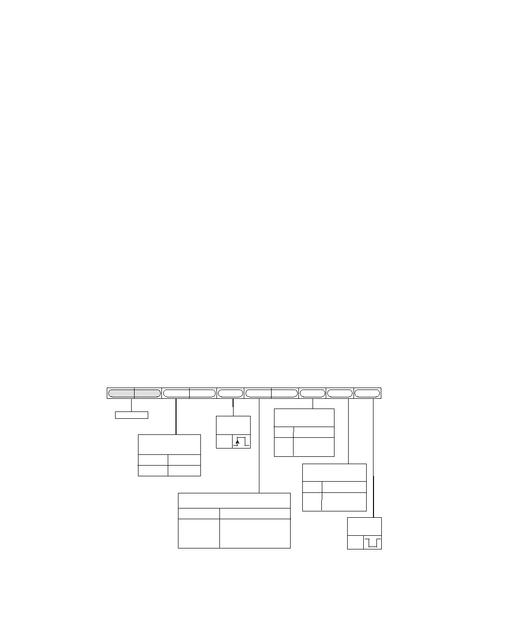
REV. 0
26
ADV7160/ADV7162
REGISTER PROGRAMMING
The following section describes each register, including Address
Register, Mode Register and each of the Control Registers in
terms of its configuration.
Address Register (A10A0)
As illustrated in the previous tables, the C1 and C0 control in-
puts, in conjunction with this address register specify which
control register, or color palette location is accessed by the
MPU port. The Address Register is 11 bits wide and can be
read from as well as written to. To access the Address Register,
two consecutive MPU accesses with C1 and C0 set to Logic "0"
are required. The first one accesses the low byte; and when a
second access of the same type is performed, i.e., two consecu-
tive reads or two consecutive writes, the high byte is accessed.
If the type of access is changed, or if an access to a different reg-
ister is inserted between the first and the second, then the sec-
ond access will access the low byte again. When writing to or
reading from the color palette on a sequential basis, only the
start address needs to be written. After a red, green and blue
write sequence, the address register is automatically incremented.
Mode Register (MR1)
The mode register is a 10-bit wide register. However for pro-
gramming purposes, it may be considered as an 8-bit wide regis-
ter (MR19 and MR18 are both reserved). It is denoted as
MR17MR10 for simplification purposes.
Figure 39 shows the various operations under the control of the
mode register. This register can be read from as well written to.
In read mode, if MR19 and MR18 are read back, they are both
returned as zeros.
MODE REGISTER BIT DESCRIPTION
Reset Control (MR10)
This bit is used to reset the pixel port sampling sequence. This
ensures that the pixel sequence ABCD starts at A. It is reset by
writing a "1" followed by a "0" followed by a "1." This bit must
run this cycle during the initialization sequence.
RAM-DAC Resolution Control (MR11)
When this is programmed with a "1," the RAM is 30 bits deep
(10 bits each for red, green and blue), and each of the three
DACs is configured for 10-bit resolution. When MR11 is pro-
grammed with a "0," the RAM is 24 bits deep (8 bits each for
red, green and blue), and the DACs are configured for 8-bit
resolution. The two LSBs of the 10-bit DACs are pulled down
to zero in 8-bit RAM-DAC mode.
MPU Data Bus Width (MR12)
This bit determines the width of the MPU port. It is configured
as either a 10-bit wide (D9D0) or 8-bit wide (D7D0) bus.
Ten-bit data can be written to the device when configured 8-bit
wide mode. The 8 MSBs are first written on D7D0, then the
two LSBs are written over D1D0. Bits D9D8 are zeros in 8-
bit mode.
Operational Mode Control (MR14MR13)
When MR14 and MR13 are "0" the part operates in normal
mode.
Calibrate LOADIN (MR15)
This bit automatically calibrates the on-board LOADIN/
LOADOUT synchronization circuit. A "0" to "1" transition
initiates calibration. This bit is set to "0" in normal operation.
See "Pipeline Delay & Calibration" section. This bit must run
this cycle during the initialization sequence.
Palette Select Match Bits Control (MR17MR16)
These bits allow multiple palette devices to work together.
When bits PS1 and PS0 match MR17 and MR16 respectively,
the device is selected. If these bits do not match, the device is
not selected and the analog video outputs drive 0 mA. See
"Palette Priority Select Inputs" section.
CONTROL REGISTERS
A large bank of registers plus the 64
×
64 cursor image can be
accessed through the Control Register. Access is made first by
writing the Address Register with the appropriate address to
point to the particular Control Register (see Figure 34), and
Figure 39. Mode Register 1 (MR1) (MR19MR10)
RESERVED*
MR19
MR18
MR17
MR16
MR12
MR15
PCR4
MR13
MR11
MR10
*
THESE BITS ARE READ-ONLY
RESERVED BITS.
A READ CYCLE WILL RETURN
ZEROS "00."
PALETTE SELECT
MATCH BITS CONTROL
MR16 PS0
MR17 PS1
MPU DATA BUS
WIDTH
MR12
0 8-BIT (D7D0)
1 10-BIT (D9D0)
OPERATIONAL MODE CONTROL
0 0
0 1
1 0
1 1
MR14 MR13
NORMAL OPERATION
RESERVED
RESERVED
RESERVED
MR14
CALIBRATE
LOADIN
MR15
RAM-DAC
RESOLUTION CONTROL
MR11
0 8-BIT
1 10-BIT
RESET
CONTROL
MR10
ADV7160/ADV7162
REV. 0
27
then performing an MPU access to the Control Register. When
accessing Control Registers in the range 200H to 204H, and
when accessing the cursor image, the Address Register auto-
increments after each register access. On accessing the last cur-
sor image location at address 7FFH, the address register reverts
to address 000H. The Address Register also auto-increments
after a blue access, when accessing color registers in the address
range 303H to 304H.
ID Register
(Address Reg (A10A0) = 003H)
This is an 8-bit wide "Identification" read-only register. For the
ADV7160 it will always return the hexadecimal value 76H. For
the ADV7162 it will always return the hexadecimal value 79H.
Pixel Mask Register
(Address Reg (A10A0) = 004H)
The contents of the pixel mask register are individually bit-wise
logically ANDed with the Red, Green and Blue pixel input
stream of data. It is an 8-bit read/write register with D0 corre-
sponding to R0, G0 and B0. For normal operation, this register
is set with FFH.
COMMAND REGISTER 1 (CR1)
(Address Reg (A10A0) = 005H)
This register contains a number of control bits as shown in the
diagram. CR1 is a 10-bit wide register. However for program-
ming purposes, it may be considered as an 8-bit wide register
(CR19 to CR18 reserved).
Figure 40 shows the various operations under the control of
CR1. This register can be read from as well written to. In write
mode zero should be written to CR12. In read mode, CR19
and CR18 are returned as zeros.
COMMAND REGISTER 1-BIT DESCRIPTION
Calibration Control (CR10)
This bit automatically calibrates the on-board LOADIN/
LOADOUT synchronization circuit on every vertical Sync.
MR15 of Mode Register MR1 must be set to "0."
Figure 40. Command Register 1 (CR1) (CR19CR10)
Hi-Byte Control (CR13)
This bit enables access to the Hi Byte of the Address Register.
When CR13 is set to Logic "0", the part is compatible to the
ADV7150. To access the hi-byte of the address register, this bit
is set to Logic "1."
PS Function Control (CR15CR14)
These bits control the functions of the PS inputs. They are
used to enable the Overlay Mode, Bypass Mode or the Palette
Select Mode. In Palette Select Mode (CR15 and CR14 = "0"),
these inputs are used to multiplex the RGB outputs of a number
of devices. On a pixel by pixel basis, PS1 and PS0 are com-
pared against the PS match bits, MR17 and MR16. If they
match, then the part behaves normally. If they don't match,
then the analog output currents are switched to zero for that
clock cycle, thus allowing another device, whose PS match bits
match during this time, to drive the monitor. In Bypass Mode
(CR15 = "0," CR14 = "1"), PS1 is used to switch between one
of the color modes through the Color Palette and one of the Pal-
ette Bypass Modes, on a pixel by pixel basis. The color mode
through the palette is selected using CR17 and CR16. It is il-
legal to program CR27 to CR24 to select one of the bypass modes
when using the PS bits to select a bypass mode at the pixel rate.
This switching on a pixel by pixel basis is only allowed when using
an ADV7160 device. Therefore, for the ADV7162, this mode
(CR15 = "0," CR14 = "1"), is reserved and should not be used.
In Overlay Mode (CR15 = "1," CR14 = "0"), the PS inputs
provide control for a three color overlay. Whenever a value
other than "00" is placed on the overlay inputs, the correspond-
ing overlay color is displayed. When the overlay inputs contain
"00," the color is specified by the pixel inputs.
When CR15 and CR14 = "1," the PS inputs are completely
ignored. There is no overlay, no bypass switching and the RGB
outputs are enabled.
Bypass Color Mode Control (CR17CR16)
These bits control the mode during bypass switching. There are
three different modes: 24-bit Bypass, 16-bit Bypass or 15-bit
Bypass Mode.
RESERVED*
CR19
CR18
CR17
CR16
CR12
CR15
CR14
CR13
CR11
CR10
*
THESE BITS ARE READ-ONLY
RESERVED BITS.
A READ CYCLE WILL RETURN
ZEROS "00."
TEST MODE CONTROL
CR11
1 ENABLE TEST
MODE
0 DISABLE
PS FUNCTION CONTROL
0 0
0 1
1 0
1 1
CR15 CR14
PALETTE SELECTS
BYPASS MODE**
OVERLAYS
IGNORE PS INPUTS
**THIS MODE IS ONLY AVAILABLE
ON THE ADV7160.
IT IS RESERVED ON THE ADV7162.
ADDRESS REGISTER
HI-BYTE CONTROL
CR13
0 NO ACCESS TO HI-BYTE
(ADV7150 COMPATIBLE)
CR12
(0)
BYPASS COLOR MODE
0 0
0 1
1 0
1 1
CR17 CR16
15-BIT BYPASS
16-BIT BYPASS
24-BIT BYPASS
RESERVED
THIS BIT SHOULD
BE SET TO ZERO
CALIBRATION
CONTROL
CR10
1 CALIBRATES ON
EVERY VERTICAL
SYNC (MR15=0)
0 DISABLE
1 ACCESS TO HI-BYTE
REV. 0
28
ADV7160/ADV7162
COMMAND REGISTER 3 (CR3)
(Address Reg (A10A0) = 007H)
This register contains a number of control bits as shown in the
diagram. CR3 is a 10-bit wide register. However for program-
ming purposes, it may be considered as an 8-bit wide register
(CR39 and CR38 are both reserved).
Figure 42 shows the various operations under the control of
CR3. This register can be read from as well written to. In write
mode zero should be written to CR35. In read mode, CR39 and
CR38 are returned as zeros.
COMMAND REGISTER 3 BIT DESCRIPTION
PRGCKOUT Frequency Control (CR31CR30)
These bits specify the output frequency of the PRGCKOUT
output. PRGCKOUT is a divided down version of the pixel
CLOCK.
BLANK
Pipeline Delay Control (CR34CR32)
These bits specify the additional pipeline delay that can be
added to the BLANK function, relative to the overall device
pipeline delay (t
PD
). As the BLANK control normally enters the
Video DAC from a shorter pipeline than the video pixel data,
this control is useful in de-skewing the pipeline differential.
Pixel Multiplex Control (CR37CR36)
These bits specify the device's multiplex mode. It therefore
also determines the frequency of the LOADOUT signal.
LOADOUT is a divided down version of the pixel CLOCK.
COMMAND REGISTER 2 (CR2)
(Address Reg (A10A0) = 006H)
This register contains a number of control bits as shown in the
diagram. CR2 is a 10-bit wide register. However for program-
ming purposes, it may be considered as an 8-bit wide register
(CR29 and CR28 are both reserved).
Figure 41 shows the various operations under the control of
CR2. This register can be read from as well written to. In write
mode zero should be written to CR21 and CR20. In read
mode, CR29 and CR28 are returned as zeros.
COMMAND REGISTER 2-BIT DESCRIPTION
SYNC
Recognition Control on Green (CR22)
This bit specifies whether the video SYNC Input is to be en-
coded onto the IOG analog output or ignored.
Pedestal Enable Control (CR23)
This bit specifies whether a 0 IRE or a 7.5 IRE blanking pedes-
tal is to be generated on the video outputs.
True-Color/Bypass/Pseudo-Color Mode Control (CR27CR24)
These 4 bits specify the various color modes. These include a
24-bit true-color and bypass mode, one 16-bit true-color and
bypass mode, two 15-bit true-color modes, one 15-bit bypass
mode and three 8-bit pseudo color modes.
Figure 41. Command Register 2 (CR2) (CR29CR20)
RESERVED*
CR29
CR28
CR27
CR26
CR20
CR25
CR24
CR21
*
THESE BITS ARE READ-ONLY RESERVED BITS.
A READ CYCLE WILL RETURN ZEROS "00."
CR21CR20
(00)
ZERO SHOULD
BE WRITTEN TO
THESE BITS
SYNC
RECOGNITION
CONTROL (GREEN)
CR22
0 IGNORE
1 DECODE
PEDESTAL ENABLE
CONTROL
CR23
0 0 IRE
1 7.5 IRE
CR27 CR26 CR25 CR24
0 0 0 0 8-BIT PSEUDO COLOR ON R7R0
0 1 0 0 8-BIT PSEUDO COLOR ON G7G0
1 0 0 0 8-BIT PSEUDO COLOR ON B70
1 0 0 1 16-BIT BYPASS MODE USING
R7R0, G7G0
1 0 1 0 15-BIT BYPASS MODE USING
R6R0, G7G0
1 0 1 1 16-BIT TRUE COLOR ON R7R0,
G7G0
1 1 0 0 15-BIT TRUE COLOR ON R7R3,
G7G3, B7B3
1 1 0 1 15-BIT TRUE COLOR ON R6R0,
G7G0
1 1 1 0 24-BIT TRUE COLOR
1 1 1 1 24-BIT BYPASS MODE
TRUE COLOR/PSEUDO COLOR MODE CONTROL
COLOR MODE
CR23
CR22
ADV7160/ADV7162
REV. 0
29
Figure 42. Command Register 3 (CR3) (CR39CR30)
COMMAND REGISTER 4 (CR4)
(ADDRESS REG (A10A0) = 008H)
This register contains a number of control bits as shown in the
diagram. CR4 is a 10-bit wide register. However for program-
ming purposes, it may be considered as an 8-bit wide register
(CR49 and CR48 are both reserved).
Figure 43 shows the various operations under the control of
CR4. This register can be read from as well written to. In read
mode, CR49 and CR48 are both returned as zeros.
COMMAND REGISTER 4-BIT DESCRIPTION
HDTV SYNC Enable (CR40)
This bit specifies whether the video TRISYNC Input is to be
encoded, enabling the DAC outputs to generate a Tri-Level
Sync.
SYNC
Recognition Control on Red (CR41)
This bit specifies whether the video SYNC Input is to be en-
coded onto the IOR analog output or ignored.
SYNC
Recognition Control on Blue (CR42)
This bit specifies whether the video SYNC Input is to be en-
coded onto the IOB analog output or ignored.
Gain Control (CR44CR43)
These bits specifies the amount of gain on the DAC depending
on the standard required. See "DAC and Video Outputs" sec-
tion for more detail. For gain settings that have no pedestal, the
pedestal is automatically disabled independently of CR23.
Signature Clock Control (CR45)
This bit enables or disables the clock to the signature analyzer.
Figure 43. Command Register 4 (CR4) (CRF49CR40)
HDTV SYNC CONTROL
SYNC RECOGNITION
CONTROL (RED)
SYNC RECOGNITION
CONTROL (BLUE)
DAC GAIN
CR44 CR43
Reserved*
CR49
CR48
CR47
CR46
CR45
CR42
CR41
CR40
SIGNATURE CLOCK
CONTROL
CR46
SIGNATURE
RESET
SIGNATURE ACQUIRE
CR47
*
THESE BITS ARE READ-ONLY
RESERVED BITS.
A READ CYCLE WILL RETURN
ZEROS "00."
CR45
CR42
CR41
CR40
0 IGNORE
1 DECODE
0 IGNORE
1 DECODE
0 DISABLE TRI-SYNC
1 ENABLE TRI-SYNC
0 ENABLE
1 DISABLE
0 DISABLE
1 ENABLE
0 DISABLE CLOCK
1 ENABLE CLOCK
0 0 3996
0 1 4224
1 0 4311
1 1 5592
CR44
CR43
RESERVED*
CR31 CR30
0 0 CLOCK
÷
4
0 1 CLOCK
÷
8
1 0 CLOCK
÷
16
1 1 CLOCK
÷
32
PRGCKOUT FREQUENCY
CONTROL
CR39
CR38
CR35
*
THESE BITS ARE READ-ONLY
RESERVED BITS.
A READ CYCLE WILL RETURN
ZEROS "00."
CR37
CR36
CR34
CR33
CR32
CR37
CR36
EXTRA
BLANK
PIPELINE DELAY CONTROL
(ADDS TO PIXEL PIPELINE DELAY; t
PD
)
0 0 0 t
PD
0 0 1 t
PD
+ 1 x LOADOUT
0 1 0 t
PD
+ 2 x LOADOUT
.........
.........
1 1 1 t
PD
+ 7 x LOADOUT
CR34 CR33 CR32
BLANK
PIPELINE DELAY
CR35
(0)
CR37 CR36
0 0 1:1 MUXING: LOADOUT = CLOCK
÷
1
0 1 2:1 MUXING: LOADOUT = CLOCK
÷
2
1 0 8:1 MUXING: LOADOUT = CLOCK
÷
8 (PSEUDO COLOR ONLY)
1 1 4:1 MUXING: LOADOUT = CLOCK
÷
4
Pixel Multiplex Control
ZERO SHOULD
BE WRITTEN TO
THIS BIT
RESERVED*
REV. 0
30
ADV7160/ADV7162
Signature Reset Control (CR46)
Taking CR46 low then high resets the signature analyzer. This is
done to give a known starting point before acquiring a signature.
Signature Acquire Control (CR47)
This bit should be set to Logic "1" for normal operation. See
"Test Diagnostic" section for more information.
COMMAND REGISTER 5 (CR5)
(Address Reg (A10A0) = 00DH)
This register contains one control bit CR56. CR5 is a 10-bit
wide register. However for programming purposes, it may be
considered as an 8-bit wide register (CR59 and CR58 are both
reserved).
This register can be read from as well written to. Control Bit
CR56 selects either external clock or internal PLL operation. If
the internal PLL is to be used, Logic "1" should be written to
CR56.This should be set up immediately after power up. In
write mode, zero should be written to CR57 and CR55CR50.
In read mode, CR59 and CR58 are both returned as zeros.
PLL COMMAND REGISTER (PCR)
(Address Reg (A10A0) = 009H)
This register contains a number of control bits as shown in the
diagram. PCR is a 10-bit wide register. However, for program-
ming purposes, it may be considered as an 8-bit wide register
(PCR9 and PCR8 are both reserved).
Figure 44 shows the various operations under the control of
PCR. This register can be read from as well written to. In write
mode zero should be written to PCR3. In read mode PCR9 and
PCR8 are returned as zeros.
PLL Control (PCR0)
This bit enables or disables PLL.
RSEL Bit Control (PCR1)
This bit enables or disables RSEL, which together with the con-
tents of the PLL R Register affect the reference divider value of
the PLL. Reference Divider = (1 + RSEL)
×
(R+2).
VSEL Bit Control (PCR2)
This bit enables or disables VSEL, which together with the
contents of the PLL V Register and the PLL S value affect the
feedback divider value of the PLL.
Feedback Divider = (1 + VSEL)
×
(4(V + 2)+S).
Output Divide Control (PCR5PCR4)
These bits control the PLL output divider. This post-scaler
is used in the generation of lower frequencies.
PLL S Control (PCR7PCR6)
These bits set up the S value in the PLL transfer function.
This extra value provides extra control in setting the feed-
back divider value of the PLL.
Status Register
(Address Reg (A10A0) = 00AH)
This register is a read only 10-bit register. However SR9
SR8 are reserved bits, containing zeros and SR7SR1 are
undefined bits and should be masked in software on read
back. Therefore, SR0 is the only relevant Bit in the Status
Register and contains a Logic "1" if one, or more of the
IOR, IOG, and IOB outputs exceed the internal voltage of
the SENSE comparator circuit . It can be used to deter-
mine the presence of a CRT monitor. With some diagnos-
tic code, the presence of loading on the individual RGB
lines can be determined. The reference is generated by a
voltage divider from the external voltage reference on the
V
REF
pin. For the proper operation, the following levels
should be applied to the comparator by the IOR, IOG and
IOB outputs:
DAC Low Voltage
250 mV
DAC High Voltage
450 mV
Revision Register
(Address Reg (A10A0) = 01BH)
This register is a read only register containing the revision
of silicon.
PLL R Register
(Address Reg (A10A0) = 00CH)
This register is a read only 10-bit register. However, R9R8
are reserved bits, containing zeros. Bit R7 is a read only bit.
This bit should be masked in software on readback as its
value may be indeterminate. Therefore, the PLL R Register
may be treated as a 7-bit wide register. This register, to-
gether with the RSEL Bit in the PLL Control Register, con-
trols the reference divider of the on-board PLL.
Figure 44. Command Register (PCR) (PCR9PCR0)
PCR9
PCR8
PCR7
PCR6
PCR2
PCR5
PCR4
PCR3
PCR1
PCR0
*
THESE BITS ARE READ-ONLY
RESERVED BITS.
A READ CYCLE WILL RETURN
ZEROS "00."
PCR5
(0)
ZERO SHOULD
BE WRITTEN TO
THIS BIT
S VALUE
PCR7 PCR6
(S1 S0)
0 0 0
0 1 1
1 0 2
1 1 3
RSEL ENABLE
PCR1
0 DISABLE
1 ENABLE
VSEL ENABLE
PCR2
0 DISABLE
1 ENABLE
PLL CONTROL
PCR0
0 DISABLE PLL
1 ENABLE PLL
F
OUT
PCR5 PCR4
(PSEL1 PSEL0)
0 0 VCO/1
0 1 VCO/2
1 0 VCO/4
1 1 VCO/8
RESERVED*
ADV7160/ADV7162
REV. 0
31
PLL V Register
(Address Reg (A10A0) = 00FH)
This register is a read only 10-bit register. However V9V8 are
reserved bits, containing zeros. Bit V7 is a read only bit. This
bit should be masked in software on readback as its value may
be indeterminate. Therefore, the PLL V Register may be treated
as a 7-bit wide register. This register, together with the VSEL
Bit in the PLL Control Register, controls the feedback divider
of the on-board PLL.
64
×
64 Cursor
The ADV7160/ADV7162 has a 64
×
64 cursor generator on
board. Several of the control registers control the cursor.
These will be described in detail. The Cursor-X and Cursor-Y
registers specify the position the cursor is to be placed on the
screen. The origin (0, 0) of the cursor is top left. The position
of the cursor is taken relative to this point, allowing the Cursor-
X and Cursor-Y registers to be programmed with negative num-
bers and thus allow the cursor to be partially or completely off
the screen. The cursor can work as an X-11 or XGA cursor,
controlled by Bits CCR0 and CCR1 of the Cursor Control
Register.
The screen X and Y coordinates are measured from the rising
edge of BLANK. The first pixel after the rising edge of BLANK
corresponds to the origin (0, 0). The Vertical retrace time is ex-
tracted from the composite SYNC and BLANK inputs. The
start of Vertical Retrace is recognized by counting a second ris-
ing edge on SYNC while BLANK remains low. The next rising
edge on BLANK is the start of line 0.
Cursor X-Lo and Cursor X-Hi Register
(Address Reg (A10A0) = 200H and 201H)
These 8-bit registers together form a 16-bit 2s complement rep-
resentation of the cursor x-coordinate on the screen. The valid
range for the cursor x-coordinate is
±
FFFH. The negative
number representation allows for part or all of the cursor to be
displayed off the left-hand edge of the screen
Cursor Y-Lo and Cursor Y-Hi Register
(Address Reg (A10A0) = 202H and 203H)
These 8-bit registers together form a 16-bit 2s complement rep-
resentation of the cursor x-coordinate on the screen. The valid
range for the cursor x-coordinate is
±
FFFH. The negative
number representation allows for part or all of the cursor to be
displayed off the top/left of the screen.
When accessing the cursor X and Y registers, the Address Regis-
ter auto-increments after each access. There are no restrictions
on updating the cursor coordinate registers other than they must
all be written in the order X-Low, X-Hi, Y-Low, Y-Hi to update
the coordinates. Only one cursor is displayed per frame, at the
last X and Y coordinates written. Access to these registers is
independent of the databus being configured for 8- or 10-bit
operation.
Cursor Color 1 and Cursor Color 2 Register
(Address Reg (A10A0) = 304H and 303H)
Each of these color registers are 30 bits wide, made up of 10 bits
for Red, 10 bits for Green and 10 bits for Blue. Access to these
registers behaves in the same way as access to the Color Palette
with respect to the different combinations of 10/8-bit databus
and 10/8-bit DAC resolution.
Cursor Image
(Address Reg (A10A0) = 400H7FFH)
This region contains the 64
×
64
×
2-bit Cursor Image. Eight
bits are stored at each address. With two bits per cursor pixel,
four horizontally adjacent pixels are stored at each address. As
each address location in the Cursor Image is filled, the progres-
sion is from left to right until a line is filled and top to bottom
until all the lines are filled. The cursor can be displayed on both
an interlaced and noninterlaced system, as controlled by CCR3
of the Cursor Control Register. On an interlaced system, only
one cursor can be displayed per field. The ODD/EVEN input
indicates which field of the frame is being displayed.
Cursor Y Coordinate Even
The Even field starts with line 0 of the cursor image on line Y of
the frame. Subsequent even lines of the cursor image are dis-
played on subsequent lines of the Even field. On the Even field,
the frame line counter starts at 0 and increments by 2 at the end
of every Even field line. The Odd field starts with line 1 of the
cursor image on line Y + 1 of the frame. Subsequent odd lines
of the cursor image are displayed on subsequent lines of the
Odd field. On the Odd field, the frame line counter starts at 1
and increments by 2 at the end of every Odd field line.
Cursor Y Coordinate Odd
The Even field starts with line 1 of the cursor image on line
Y + 1 of the frame. Subsequent even lines of the cursor image
are displayed on subsequent lines of the Even field. On the
Even field, the frame line counter starts at 1 and increments by
2 at the end of every Even field line. The Odd field starts with
line 0 of the cursor image on line Y of the frame. Subsequent
odd lines of the cursor image are displayed on subsequent lines
of the Odd field. On the Odd field, the frame line counter starts
at 0 and increments by 2 at the end of every Odd field line.
Cursor Control Register
(Address Reg (A10A0) = 204H)
This register contains a number of control bits. CCR is a 10-bit
wide register. However for programming purposes, it may be
considered as an 8-bit wide register (CCR8 and CCR9 are both
reserved). In write mode zero should be written to CCR4 to
CCR7. In read mode, CCR8 and CCR9 are all returned as
zeros.
Figure 45 shows the various operations under the control of
CCR.
CURSOR CONTROL REGISTER BIT DESCRIPTION
CURSOR MODE CONTROL (CCR1CCR0)
These bits specify which type of cursor is being used. Each cur-
sor pixel value controls the color differently in each mode.
Table II.
Bit 1
Bit 0
X-11 Cursor
XGA Cursor
0
0
Transparent
Color 1
0
1
Transparent
Color 2
1
0
Color 1
Transparent
1
1
Color 2
Bit-Wise Complement
Cursor Enable Control (CCR2)
This bit turns the cursor on and off.
Interlace Control (CCR3)
This bit determines whether the cursor is being used in inter-
laced or noninterlaced mode.
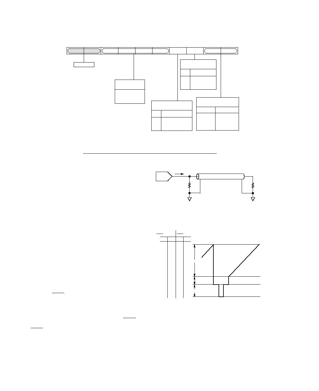
REV. 0
32
ADV7160/ADV7162
Figure 45. Cursor Control Register (CCR) (CCR9CCR0)
IOR, IOG, IOB
Z
O
= 75
(CABLE)
ZS = 75
(SOURCE TERMINATION)
Z
L
= 75
(MONITOR)
DACs
Figure 46. DAC Output Termination
(Doubly Terminated 75
Load)
Figure 47. Composite Video Waveform SYNC Decoded;
Pedestal = 7.5 IRE; DAC Gain = 3996
DIGITAL-TO-ANALOG
CONVERTER (DACS) AND
VIDEO OUTPUTS
The ADV7160/ADV7162 contains three high speed video
DACs. The DAC outputs are represented as the three primary
analog color signals IOR (red video), IOG (green video) and
IOB (blue video).
DACs and Analog Outputs
The part contains three matched 10-bit digital-to-analog con-
verters. The DACs are designed using an advanced, high speed,
segmented architecture. The bit currents corresponding to each
digital input are routed to either IOR, IOG, IOB (bit = "1") or
GND.
The analog video outputs are high impedance current sources.
Each of the these three RGB current outputs are specified to di-
rectly drive a 37.5
load (doubly terminated 75
).
Reference Input and R
SET
An external 1.23 V voltage reference is required to set up the
analog outputs of the ADV7160/ADV7162. The reference volt-
age is connected to the V
REF
input.
A resistor R
SET
is connected between the R
SET
input of the part
and ground. For specified performance, R
SET
has a value of
280
. This corresponds to the generation of RS-343A video
levels (with SYNC on IOG and Pedestal = 7.5 IRE) into a dou-
bly terminated 75
load. In this example DAC Gain has a
value of 3996 and is set using CR43 and CR44 of Command
Register 4. Figure 47 illustrates the resulting video waveform
and the Video Output Truth Table illustrates the corresponding
control input stimuli. On the ADV7160/ADV7162 SYNC can
be encoded on any of the analog signals, however in practice,
SYNC
is generally encoded on either the IOG output or on all
of the video outputs.
CCR9
CCR8
CCR7
CCR6
CCR2
CCR3
CCR0
CCR5
CCR4
CCR1
*
THESE BITS ARE READ-ONLY
RESERVED BITS.
A READ CYCLE WILL RETURN
ZEROS "00."
CCR7CCR4
(0000)
ZERO SHOULD
BE WRITTEN TO
THESE BITS
CURSOR ENABLE
CCR2
0 DISABLE
1 ENABLE
CURSOR CONTROL
CCR3
0 NONINTERLACED
1 INTERLACED
CCR1 CCR0
CURSOR MODE
Control
0 0 RESERVED
0 1 X11 CURSOR
1 0 XGA CURSOR
1 1 RESERVED
RESERVED*
92.5 IRE
7.5 IRE
40 IRE
0.340
9.05
0.054
1.44
0.286
7.62
0
0
1.000
26.67
0.714
19.05
0
0
mA
V
mA
V
OUTPUT WITHOUT
SYNC
ENCODED
OUTPUT WITH
SYNC
ENCODED
WHITE
LEVEL
BLACK
LEVEL
BLANK
LEVEL
SYNC
LEVEL
GREY SCALE
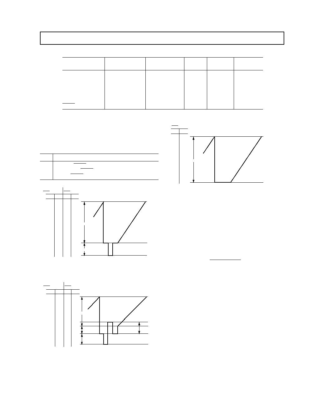
ADV7160/ADV7162
REV. 0
33
Table III. Video Output Truth Table
O/P with Sync
O/P with Sync
SYNC
BLANK
DAC
Description
Enabled (mA)
Disabled (mA)
Input Data
WHITE LEVEL
26.67
19.05
1
1
3FFH
VIDEO
Video + 9.05
Video + 1.44
1
1
Data
VIDEO to BLANK
Video + 1.44
Video + 1.44
0
1
Data
BLACK LEVEL
9.05
1.44
1
1
000H
BLACK to BLANK
1.44
1.44
0
1
000H
BLANK LEVEL
7.62
0
1
0
xxxH
SYNC
LEVEL
0
0
0
0
xxxH
Variations on RS-343A
Various other video output configurations can be implemented
by the ADV7160/ADV7162, including RS-170. The table
shows calculated values of DAC Gain for some of the most
common variants on the RS-343A standard. The associated
waveforms are shown in the diagrams.
Gain
Video Signal
4224
RS343A, SYNC decoded on output; Pedestal = 0 IRE
4311
RS343A, No SYNC decoded; Pedestal = 0 IRE
5592
RS170, SYNC decoded; Pedestal = 7.5 IRE
100 IRE
43 IRE
0.302
8.05
0
0
1.000
26.67
0.698
18.62
0
0
mA
V
mA
V
OUTPUT WITHOUT
SYNC
ENCODED
OUTPUT WITH
SYNC
ENCODED
WHITE
LEVEL
BLANK/
BLACK
LEVEL
SYNC
LEVEL
GREY SCALE
Figure 48. Composite Video Waveform SYNC
Decoded; Pedestal = 0 IRE; DAC Gain = 4224
92.5 IRE
40 IRE
0.400
10.67
0
0
1.400
37.33
1.00
26.67
0
0
mA
V
mA
V
OUTPUT WITHOUT
SYNC
ENCODED
OUTPUT WITH
SYNC
ENCODED
WHITE
LEVEL
BLANK
LEVEL
SYNC
LEVEL
7.5 IRE
BLACK
LEVEL
TRISYNC
LEVEL
0.475
12.67
0.075
2.00
0.800
21.24
GREY SCALE
Figure 49. Composite Video Waveform SYNC and
TRISYNC decoded; Pedestal = 7.5 IRE; DAC Gain = 5592
GREY SCALE
100 IRE
0
0
0.714
19.05
mA
V
OUTPUT WITHOUT
SYNC
ENCODED
WHITE LEVEL
BLANK/BLACK
LEVEL
Figure 50. Composite Video Waveform Pedestal = 0
IRE; DAC Gain = 4311
Output Currents
The various output currents are set by V
REF
, R
SET
and the DAC
gain. By programming the Command Register Bits and choos-
ing the correct DAC Gain value, video waveforms conforming
to the common variations on RS-170 and RS-343A, as well as
HDTV standards may be generated. The currents generated
can be summarized as:
I
OUT
=
I
DAC
+
I
BLANK
+
I
SYNC
+
I
TRISYNC
I
DAC
(mA)
=
DAC GAIN
×
V
REF
R
SET
I
BLANK
(mA)
=
0.0817
×
I
DAC
I
SYNC
(mA)
=
0.4322
×
I
DAC
I
TRISYNC
(mA)
=
0.4322
×
I
DAC

REV. 0
34
ADV7160/ADV7162
APPENDIX 1
BOARD DESIGN AND LAYOUT CONSIDERATIONS
The ADV7160/ADV7162 is a highly integrated circuit contain-
ing both precision analog and high speed digital circuitry. It has
been designed to minimize interference effects on the integrity
of the analog circuitry by the high speed digital circuitry. It is
imperative that these same design and layout techniques be ap-
plied to the system level design such that high speed, accurate
performance is achieved. The "Recommended Analog Circuit
Layout" shows the analog interface between the device and
monitor.
The layout should be optimized for lowest noise on the
ADV7160/ADV7162 power and ground lines by shielding the
digital inputs and providing good decoupling. The lead length
between groups of V
AA
and GND pins should by minimized so
as to minimize inductive ringing.
Ground Planes
The ground plane should encompass all ADV7160/ADV7162
ground pins, voltage reference circuitry, power supply bypass
circuitry for the ADV7160/ADV7162, the analog output traces,
and all the digital signal traces leading up to the ADV7160/
ADV7162. The ground plane is the graphics board's common
ground plane.
Power Planes
The ADV7160/ADV7162 and any associated analog circuitry
should have it's own power plane, referred to as the analog
power plane (V
AA
). This power plane should be connected to
the regular PCB power plane (V
CC
) at a single point through a
ferrite bead. This bead should be located within three inches of
the ADV7160/ADV7162.
The PCB power plane should provide power to all digital logic
on the PC board, and the analog power plane should provide
power to all ADV7160/ADV7162 power pins and voltage refer-
ence circuitry.
Plane-to-plane noise coupling can be reduced by ensuring that
portions of the regular PCB power and ground planes do not
overlay portions of the analog power plane, unless they can be
arranged such that the plane-to-plane noise is common mode.
Supply Decoupling
For optimum performance, bypass capacitors should be in-
stalled using the shortest leads possible, consistent with reliable
operation, to reduce the lead inductance. Best performance is
obtained with 0.1
µ
F ceramic capacitor decoupling. Each group
of V
AA
pins on the ADV7160/ADV7162 must have at least one
0.1
µ
F decoupling capacitor to GND. These capacitors should
be placed as close as possible to the device.
It is important to note that while the ADV7160/ADV7162 con-
tains circuitry to reject power supply noise, this rejection de-
creases with frequency. If a high frequency switching power
supply is used, the designer should pay close attention to reduc-
ing power supply noise and consider using a three terminal volt-
age regulator for supplying power to the analog power plane.
Digital Signal Interconnect
The digital inputs to the ADV7160/ADV7162 should be iso-
lated as much as possible from the analog outputs and other
analog circuitry. Also, these input signals should not overlay the
analog power plane.
Due to the high clock rates involved, long clock lines to the
ADV7160/ADV7162 should be avoided to reduce noise pickup.
Any active termination resistors for the digital inputs should be
connected to the regular PCB power plane (V
CC
), and not the
analog power plane.
Analog Signal Interconnect
The ADV7160/ADV7162 should be located as close as possible
to the output connectors to minimize noise pickup and reflec-
tions due to impedance mismatch.
The video output signals should overlay the ground plane, and
not the analog power plane, to maximize the high frequency
power supply rejection.
Digital Inputs, especially Pixel Data Inputs and clocking signals
(CLOCK, LOADOUT, LOADIN, etc.) should never overlay
any of the analog signal circuitry and should be kept as far away
as possible.
For best performance, the analog outputs (IOR, IOG, IOB)
should each have a 75
load resistor connected to GND.
These resistors should be placed as close as possible to the
ADV7160/ADV7162 so as to minimize reflections.
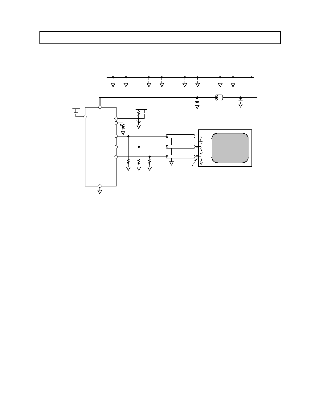
ADV7160/ADV7162
REV. 0
35
Recommended Analog Circuit Layout
ADV7160
V
REF
R
SET
IOR
IOG
IOB
COMP
V
AA
GND
R
SET
280
AD589
(1.2V REF)
0.1µF
1k
(1% METAL)
+5V (V
AA
)
75
75
75
+5V (V
AA
)
0.1µF
0.1µF
0.01µF
0.1µF
0.01µF
0.1µF
0.01µF
0.1µF
0.01µF
33µF
0.1µF
75
75
75
MONITOR (CRT)
BNC
CONNECTORS
L1 (FERRITE BEAD)
+5V (V
AA
)
+5V (V
CC
)
ANALOG POWER PLANE
POWER SUPPLY DECOUPLING (0.1µF CAPACITOR FOR EACH V
AA
GROUP)
NOTES:
1. ALL RESISTERS ARE 1% METAL FILM
2. 0.1µF AND 0.01µF CAPACITORS ARE CERAMIC
3. ADDITIONAL DIGITAL CIRCUITRY OMITTED FOR CLARITY
COAXIAL CABLE
(75
)
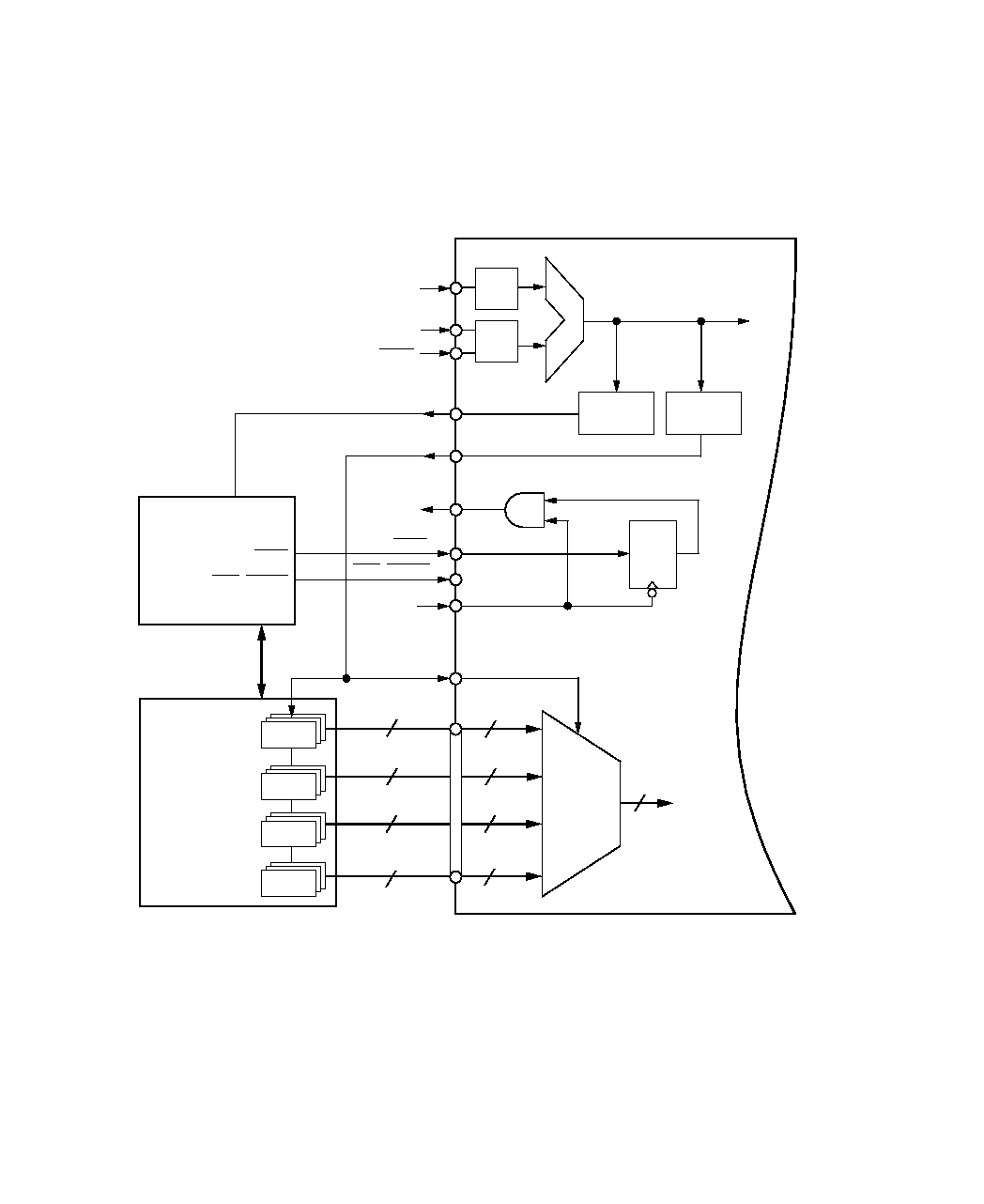
REV. 0
36
ADV7160/ADV7162
APPENDIX 2
TYPICAL FRAME BUFFER INTERFACE
ADV7160/
ADV7162
LOADOUT
DIVIDE BY M
(
÷
M)
LOADIN
BLANK
SCKOUT
SCKIN
LATCH
ENABLE
MULTIPLEXER
24
24
24
24
24
VRAM
(BANK D)
50 MHZ
VRAM
(BANK A)
50 MHZ
VRAM
(BANK B)
50 MHZ
VRAM
(BANK C)
50 MHZ
TO
PALETTE/RAM &
DAC
24
24
24
24
GRAPHICS
PROCESSOR/
CONTROLLER
CLOCK
BLANK
FRAME BUFFER/
VIDEO MEMORY
SYNC
/
TRISYNC
SYNC
/
TRISYNC
CLOCK
CLOCK
ECL
TO
TTL
PRGCKOUT
S
E
L
E
C
T
PLL
REF
DIVIDE BY N
(
÷
N)
PLL
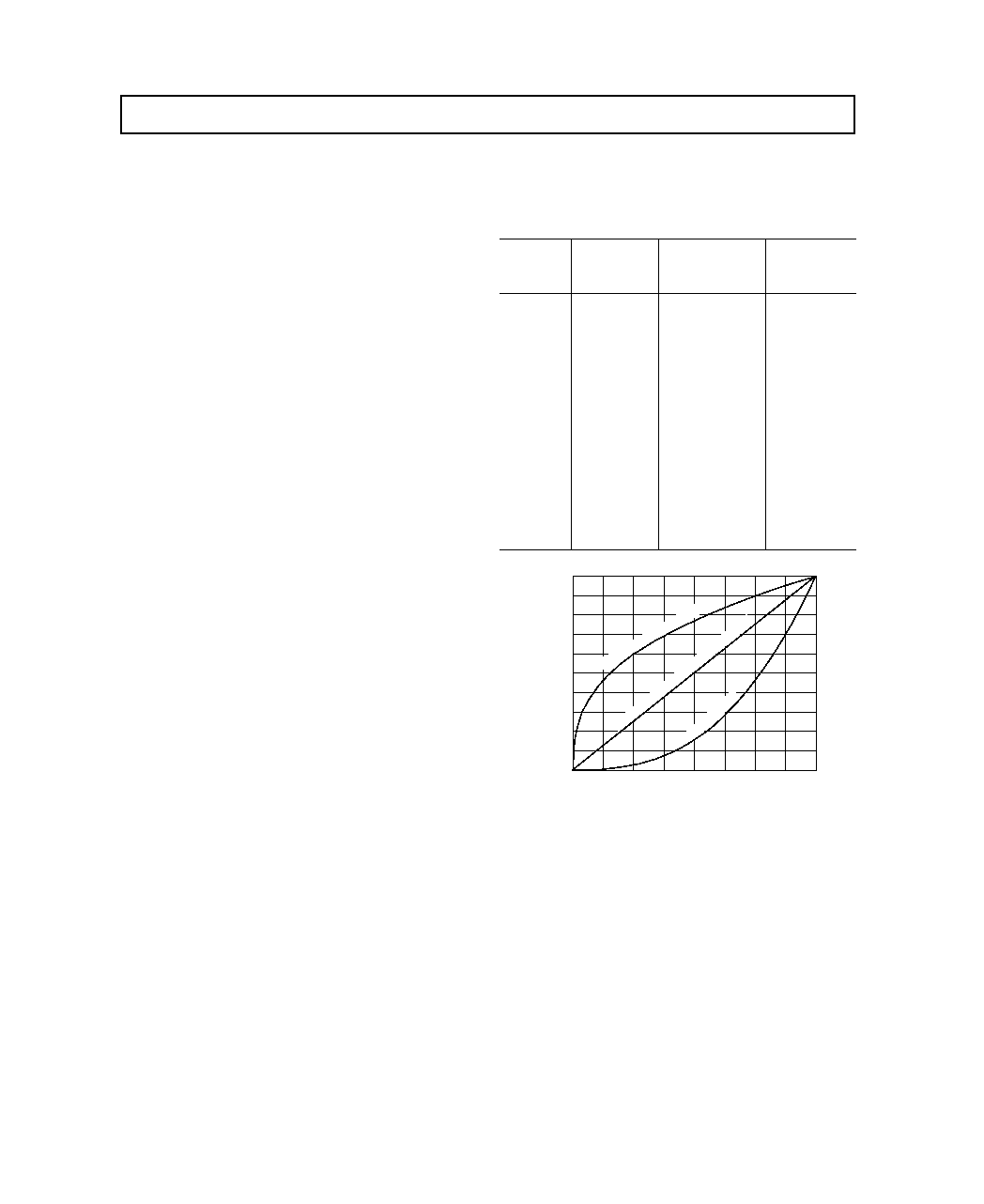
ADV7160/ADV7162
REV. 0
37
GAMMA CORRECTION
8 Bits vs. 10 Bits
Gamma
Corrected
Quantized to
Quantized to
8-Bit Data
(2.7)
8 Bits
10 Bits
240
0.977797
250
1001
241
0.979304
250
1002
242
0.980807
251
1004
243
0.982306
251
1005
244
0.983801
251
1007
245
0.985292
252
1008
246
0.986780
252
1010
247
0.988264
252
1011
248
0.989744
253
1013
249
0.991220
253
1015
250
0.992693
254
1016
251
0.994161
254
1018
252
0.995626
254
1019
253
0.997088
255
1021
254
0.998546
255
1022
255
1.000000
255
1023
INPUT CODE DECIMAL
DAC OUTPUT NORMALISED TO 1)
1.00
0.20
0
256
32
64
96
128
160
192
224
0.90
0.60
0.50
0.40
0.30
0.80
0.70
GAMMA CORRECTION CURVE
CRT RESPONSE
LINEAR RESPONSE RECIEVED BY THE EYE
0.00
0.10
Gamma Correction Curve (Gamma Value = 2.7)
APPENDIX 3
10-BIT DACs AND GAMMA CORRECTION
10-Bit DACs
10-Bit RAM-DAC resolution allows for nonlinear video correc-
tion, in particular Gamma Correction. The ADV7160/ADV7162
allows for an increase in color resolution from 24-bit to 30-bit
effective color without the necessity of a 30-bit deep frame
buffer. In true-color mode, for example, the part effectively op-
erates as a 24-bit to 30-bit color look-up table.
Up to now we have assumed that there exists a linear relation-
ship between the actual RGB values input to a monitor and the
intensity produced on the screen. This, however, is not the
case. Half scale digital input (1000 0000) might correspond to
only 20% output intensity on the CRT (Cathode Ray Tube).
The intensity (I
CRT
) produced on a CRT by an input value I
IN
is
given by:
I
CRT
= (I
IN
)
c
where c ranges from 2.0 to 2.8.
If the individual values of c for red, green and blue are known,
then so called "Gamma Correction" can be applied to each of
the three video input signals (I
IN
); therefore:
I
IN(corrected)
= k(I
IN
)
1/c
Traditionally, there has been a trade-off between implementing
a nonlinear graphics function, such as gamma correction, and
color dynamic range. The ADV7160/ADV7162 overcomes this
by increasing the individual color resolution of each of the red,
green and blue primary colors from 8 bits per color channel to
10 bits per channel (24 bits to 30 bits).
The table highlights the loss of resolution when 8-bit data is
gamma-corrected to a value of 2.7 and quantized in a traditional
8-bit system. Note that there is no change in the 8-bit quan-
tized data for linear changes in the input data over much of the
transfer function. On the other hand, when quantized to 10 bits
via the 10-bit RAMs and 10-bit DACs of the ADV7160/
ADV7162, all changes on the input 8-bit data are reflected in
corresponding changes in the 10-bit data.
The graph shows a typical gamma curve corresponding to a
gamma value of 2.7. This is programmed to the red, green and
blue RAMs of the color look-up table instead of the more tradi-
tional linear function. Different curves corresponding to any
particular gamma value can be independently programmed to
each of the red, green and blue RAMs.
Other applications of the 10-bit RAM-DAC include closed-loop
monitor color calibration.

REV. 0
38
ADV7160/ADV7162
APPENDIX 4
INITIALIZATION AND PROGRAMMING
ADV7160/ADV7162 INITIALIZATION
After power has been supplied, the ADV7160/ADV7162 must be initialized. The Mode Register and Control Registers must then
be set up. The values written to the various registers will be determined by the desired operating mode of the part, i.e., True-Color/
Pseudo-Color, 4:1 Muxing/2:1 Muxing, PLL on/off, Bypass Mode on/off etc. . . .
The following section gives a recommended initialization of the ADV7160/ADV7162 and an example of the ADV7162 operating in a
specific mode.
ADV7160/ADV7162 Initialization
C1 C0
R/W Comment
Write (xx000xx1)* to Mode Register (MR1)
1
1
0
Resets ADV7160/62
Write (xx000xx0)* to Mode Register (MR1)
1
1
0
Write (xx000xx1)* to Mode Register (MR1)
1
1
0
Write 05H to Address Register (A7A0)
0
0
0
Address Reg points to Command Register 1 (CR1)
Write (xxxx100x)* to Command Register 1 (CR1)
0
0
0
Address Reg points to CR1 for high byte access
Write 06H to Address Register (A7A0)
0
0
0
Write 00H to Address Register (A10A8)
0
0
0
Address Reg points to Command Register 2 (CR2)
Write (xxxxxx00)* to Command Reg 2 (CR2)
1
0
0
Setup CR2 as required
Write 07H to Address Register (A7A0)
0
0
0
Write 00H to Address Register (A10A8)
0
0
0
Address Reg points to Command Register 3 (CR3)
Write (xx0xxxxx)* to Command Reg 3 (CR3)
1
0
0
Setup CR3 as required
Write 08H to Address Register (A7A0)
0
0
0
Write 00H to Address Register (A10A8)
0
0
0
Address Reg points to Command Register 4 (CR4)
Write (xxxxxxxx)* to Command Reg 4 (CR4)
1
0
0
Setup CR4 as required
Write 0DH to Address Register (A7A0)
0
0
0
Write 00H to Address Register (A10A8)
0
0
0
Address Reg points to Command Register 5 (CR5)
Write (0x000000)* to Command Reg 5 (CR5)
1
0
0
Setup CR 5 as required
Write 04H to Address Register (A7A0)
0
0
0
Write 00H to Address Register (A10A8)
0
0
0
Address Reg points to Pixel Mask Register
Write (xxxxxxxx)* to Pixel Mask Register
1
0
0
Set up Pixel Mask as required
Write 04H to Address Register (A7A0)
0
0
0
Necessary only if CCR to be used
Write 02H to Address Register (A10A8)
0
0
0
Address Reg points to Cursor Control Register (CCR)
Write (xxxxxxxx)* to Cursor Control Register
1
0
0
Set up CCR as required
Write 0FH to Address Register (A7A0)
0
0
0
Necessary only if PLL to be used
Write 00H to Address Register (A10A8)
0
0
0
Address Reg points to PLL V Register
Write (xxxxxxxx)* to PLL V Register
1
0
0
Set up V as required
Write 0CH to Address Register (A7A0)
0
0
0
Necessary only if PLL to be used
Write 00H to Address Register (A10A8)
0
0
0
Address Reg points to PLL R Register
Write (xxxx0xxx)* to PLL R Register
1
0
0
Set up R as required
Write 09H to Address Register (A7A0)
0
0
0
Necessary only if PLL to be used
Write 00H to Address Register (A10A8)
0
0
0
Address Reg points to PLL Command Register (PCR)
Write (xxxxxxxx)* to PLLCommand Register
1
0
0
Set up PCR as required
Write (xx0xxxxx)* to Mode Register (MR1)
1
1
0
Necessary only if manual claibration is required
Write (xx1xxxxx)* to Mode Register (MR1)
1
1
0
Toggles MR15
Write (xx0xxxxx)* to Mode Register (MR1)
1
1
0
*x represents either a 0 or 1 value that the bit should be set to, depending on the desired operating mode of the ADV7160/ADV7162.

ADV7160/ADV7162
REV. 0
39
Example
Color Mode: 24-Bit Gamma Corrected True Color (30-Bits) through Color Palette
Multiplexing: 2:1, Databus: 10-Bit, RAM-DAC Resolution: 10-Bit,
SYNC: on Green, Pedestal: 0 IRE, Calibration: Every Vertical Sync, Internal PLL: 220 MHz (Reference = 15 MHz)
Register Initialization
C1 C0
R/W
Comment
Write 07H to Mode Register (MR1)
1
1
0
Resets ADV7162*
Write 06H to Mode Register (MR1)
1
1
0
10-Bit Data Bus, 10-Bit DAC Resolution
Write 07H to Mode Register (MR1)
1
1
0
Write 05H to Address Register (A7A0)
0
0
0
Address Reg points to Command Register 1 (CR1)
Write 09H to Command Register 1 (CR1)
0
0
0
High byte access, Calibrate every Vertical Sync
Write 06H to Address Register (A7A0)
0
0
0
Write 00H to Address Register (A10A8)
0
0
0
Address Reg points to Command Register 2 (CR2)
Write E4H to Command Reg 2 (CR2)
1
0
0
24-Bit True Color, 0 IRE, Sync on Green
Write 07H to Address Register (A7A0)
0
0
0
Write 00H to Address Register (A10A8)
0
0
0
Address Reg points to Command Register 3 (CR3)
Write 40H to Command Reg 3 (CR3)
1
0
0
2:1 Muxing, PRGCKOUT = CLOCK
÷
4
Write 08H to Address Register (A7A0)
0
0
0
Write 00H to Address Register (A10A8)
0
0
0
Address Reg points to Command Register 4 (CR4)
Write 00H to Command Reg 4 (CR4)
1
0
0
DAC GAIN = 3996
Write 0DH to Address Register (A7A0)
0
0
0
Write 00H to Address Register (A10A8)
0
0
0
Address Reg points to Command Register 5 (CR5)
Write 40H to Command Reg 5 (CR5)
1
0
0
Internal PLL to be used
Write 04H to Address Register (A7A0)
0
0
0
Write 00H to Address Register (A10A8)
0
0
0
Address Reg points to Pixel Mask Register
Write FFH to Pixel Mask Register
1
0
0
Set up Pixel Mask
Write 0FH to Address Register (A7A0)
0
0
0
Write 00H to Address Register (A10A8)
0
0
0
Address Reg points to PLL V Register
Write 09H to PLL V Register
1
0
0
Set up V value
Write 0CH to Address Register (A7A0)
0
0
0
Write 00H to Address Register (A10A8)
0
0
0
Address Reg points to PLL R Register
Write 01H to PLL R Register
1
0
0
Set up R value
Write 09H to Address Register (A7A0)
0
0
0
Write 00H to Address Register (A10A8)
0
0
0
Address Reg points to PLL Command Register (PCR)
Write 06H to PLL Command Register
1
0
0
Set up PCR as required
Color Palette RAM Initialization
C1 C0
R/W
Comment
Write 00H to Address Register (A7A0)
0
0
0
Write 00H to Address Register (A10A8)
0
0
0
Points to Color Palette RAM
Write 00H (red data) to RAM location (00H)
0
1
0
(Initializes Palette RAM
Write 00H (green data) to RAM location (00H)
0
1
0
(to a Linear Ramp**
Write 00H (blue data) to RAM location (00H)
0
1
0
(
Write 01H (red data) to RAM location (01H)
0
1
0
(
Write 01H (green data) to RAM location (01H)
0
1
0
(
Write 01H (blue data) to RAM location (01H)
0
1
0
(
.
.
.
(
.
.
.
(
Write FFH (red data) to RAM location (FFH)
0
1
0
(
Write FFH (green data) to RAM location (FFH)
0
1
0
(
Write FFH (blue data) to RAM location (FFH)
0
1
0
( RAM Initialization Complete
*
*These command lines reset the ADV7162. The pipelines for each of the Red, Green & Blue pixel inputs are synchronously reset to the Multiplexer's "A" input.
Mode Register bit MR10 is written by a "1" followed by "0" followed by "1."
**This sequence of instructions would, of course, normally be coded using some form of loop instruction.
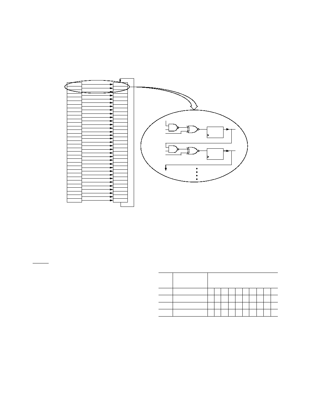
REV. 0
40
ADV7160/ADV7162
3. CR45 of Command Register 4 is set to Logic "0" during the
following vertical retrace and the acquired signature is read.
At least 20 clock cycles should be allowed for the final pixels
of the frame to travel down the pipeline of the ADV7160/
ADV7162 before the signature clock is disabled.
The signature analyzer is read from control registers 010H to
013H. These are read only 10-bit registers. The access to these
registers depends whether the part is in 8-bit or 10-bit data bus
mode and operates in the same way as accessing the color palette.
Address
Register
CONTROL
(A10A0) REGISTERS
CONTENTS
0013H
Signature Misc Register
0
0
0
0
0
0
0
S32 S31 S0
0012H
Signature Blue Register
S10 S9
S8
S7
S6
S5
S4
S3
S2
S1
0011H
Signature Green Register S20 S19 S18 S17 S16 S15 S14 S13 S12 S11
0010H
Signature Red Register
S30 S29 S28 S27 S26 S25 S24 S23 S22 S21
APPENDIX 5
SIGNATURE ANALYZER
Signature Register
The ADV7160/ADV7162 contains onboard circuitry that enables
both device and system level test diagnostics. The ADV7160/
ADV7162 has a signature analyzer in the pixel datapath, just
before the DAC decoders. The signature analyzer consists of a
33-bit linear feedback shift register. The 30-bit pixel value is
fed as a parallel input into the analyzer. The signature analyzer
only accumulates a signature during active display time when
BLANK
is high. Bit CR45 to CR47 of Command Register 4
control the signature analyzer. When CR45 of Command Reg-
ister 4 is set to Logic "1," the clock to the signature analyzer is
enabled. Toggling CR46 low and then high resets the signature
analyzer. This is done to give a known starting point before ac-
quiring a signature. CR47 of Command Register 4 controls the
feedback inputs to the analyzer. When CR47 of Command
Register 4 is a Logic "0," the feedback is disabled and on each
clock cycle, the 30-bit pixel value is latched directly into the
analyzer. To acquire a signature as the analyzer is clocked,
CR47 of Command Register 4 is set to Logic "1." To acquire a
signature the following procedure must be followed:
1. CR45 and CR47 of Command Register 4 are set to Logic
"1" during vertical retrace and CR46 of Command Register
4 is toggled to reset the analyzer.
2. A signature is acquired during the following active screen.
CR42
S19
S32
S0
CR42
B0
S1
S19
B0
B1
B2
B3
B4
B5
B6
B7
B8
B9
G0
G1
G2
G3
G4
G5
G6
G7
G8
G9
R0
R1
R2
R3
R4
R5
R6
R7
R8
R9
'0'
'0'
S0
S1
S2
S3
S4
S5
S6
S7
S8
S9
S10
S11
S12
S13
S14
S15
S16
S17
S18
S19
S20
S21
S22
S23
S24
S25
S26
S27
S28
S29
S30
S31
S32
SIGNATURE
REGISTER I/P
SIGNATURE
CELL
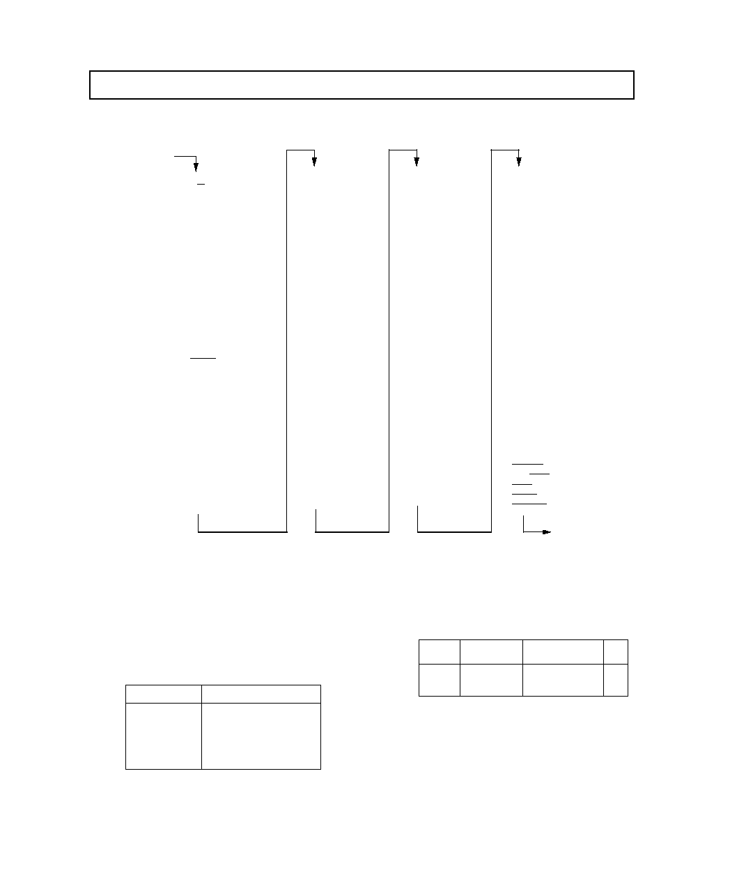
ADV7160/ADV7162
REV. 0
41
JTAG Test Port
JTAG Test Port is a 4-pin interface consisting of:
TCK: Test Clock
TMS: Test Mode Select
TDI: Test Data Input
TDO: Test Data Output
To put the ADV7160/ADV7162 into the required mode, the In-
struction Register must be loaded.
INSTRUCTION
EXTEST
SAMPLE/PRELOAD
IDCODE
PRIVATE 1
BYPASS
BYPASS
BYPASS
BYPASS
INSTRUCTION REGISTER CODE
000
001
010
011
100
101
110
111
The ADV7160 implementation has the mandatory instructions:
Bypass, Sample/Preload and Extest, and the optional instruc-
tion: IDCode. There is also one private instruction: Private1.
The Private1 instruction is for internal use in production test
only.
The IDCode is a 32-bit number which can be scanned out
through TDO. Its contents are defined below:
VERSION
(4 BITS)
1H
1H
PART NUMBER
(16 BITS)
2776H
2779H
MANUFACTURER ID
(11 BITS)
0E5H
0E5H
LSB
1H
1H
ADV7160
ADV7162
The Boundary Scan Chain is a fundamental feature of the
JTAG Test Port. It allows all the digital input and output pins
on the part to be connected into a shift register between the
TDI and TDO pins. The digital pins can be sampled, or con-
trolled over the JTAG port to carry out testing. The is no
boundary scan cell on the PLL
REF
pin. The Three-State Control
cell controls the three-state status of the microport databus.
There are 131 cells in total on the Boundary Scan Chain.
APPENDIX 6
JTAG TEST PORT (IEEE1149.1)
CE
R/
W
C0
C1
D9
D8
D7
D6
D5
D4
D3
D2
D1
D0
THREE-STATE CONTROL
LOADIN
SCKIN
SCKOUT
CLOCK
CLOCK
LOADOUT
PRGCKOUT
PS0
A
PS0
B
PS0
C
PS0
D
PS1
A
PS1
B
PS1
C
PS1
D
R0
A
R0
B
R0
C
R0
D
R1
A
R1
B
R1
C
R1
D
R2
A
R2
B
R2
C
R2
D
R3
A
R3
B
R3
C
R3
D
R4
A
R4
B
R4
C
R4
D
R5
A
R5
B
R5
C
R5
D
R6
A
R6
B
R6
C
R6
D
R7
A
R7
B
R7
C
R7
D
G0
A
G0
B
G0
C
G0
D
TDI
G1
A
G1
B
G1
C
G1
D
G2
A
G2
B
G2
C
G2
D
G3
A
G3
B
G3
C
G3
D
G4
A
G4
B
G4
C
G4
D
G5
A
G5
B
G5
C
G5
D
G6
A
G6
B
G6
C
G6
D
G7
A
G7
B
G7
C
G7
D
B0
A
B0
B
B0
C
B0
D
B1
A
B1
B
B1
C
B1
D
B2
A
B2
B
B2
C
B2
D
B3
A
B3
B
B3
C
B3
D
B4
A
B4
B
B4
C
B4
D
B5
A
B5
B
B5
C
B5
D
B6
A
B6
B
B6
C
B6
D
B7
A
B7
B
B7
C
B7
D
TRISYNC
ODD/
EVEN
SYNC
BLANK
SYNCOUT
TDO
JTAG Boundary Scan Chain
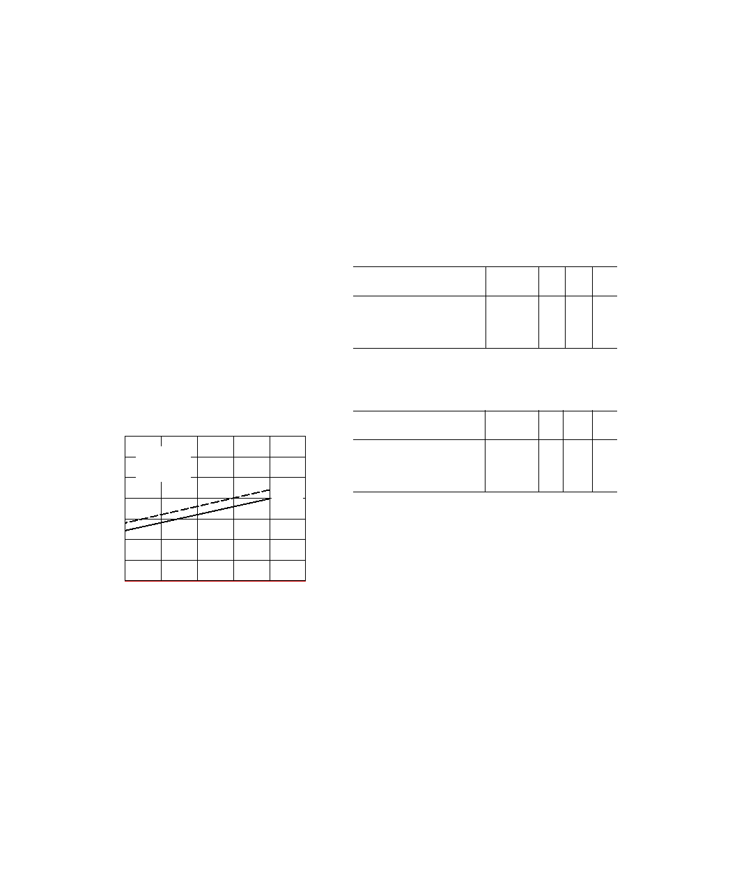
REV. 0
42
ADV7160/ADV7162
APPENDIX 7
THERMAL AND ENVIRONMENTAL CONSIDERATIONS
The ADV7160/ADV7162 is a very highly integrated monolithic
silicon device. This high level of integration, in such a small
package, inevitably leads to consideration of thermal and envi-
ronmental conditions which the ADV7160/ADV7162 must op-
erate in. Reliability of the device is enhanced by keeping it as
cool as possible. In order to avoid destructive damage to the de-
vice, the absolute maximum junction temperature of 150
°
C
must never be exceeded. Certain applications, depending on
ambient temperature and pixel data rates may require forced air
cooling or external heatsinks. The following data is intended as
a guide in evaluating the operating conditions of a particular ap-
plication so that optimum device and system performance is
achieved.
It should be noted that information on package characteristics
published herein may not be the most up to date at the time of
reading this. Advances in package compounds and manufacture
will inevitably lead to improvements in the thermal data. Please
contact your local sales office for the most up-to-date information.
Power Dissipation
The diagrams show graphs of power dissipation in watts versus
pixel clock frequency for the ADV7160 and ADV7162. When
using the ADV7162 in Bypass Mode, the Pixel Mask Register
should be programmed to 00H to reduce power further.
PIXEL CLOCK FREQUENCY MHz
2.00
0.50
60
100
140
180
220
1.50
1.25
1.00
0.75
1.75
260
2.25
POWER DISSIPATION Watts
V
AA
= +5V
V
REF
= +1.2V
T
A
= +25
°
C
ADV7160
ADV7162
Note:
The "Worst Case On-Screen Pattern" corresponds
to full-scale transition on each pixel value for
every CLOCK edge (00H, FFH, 00H, ...).
The "Typical On-Screen Pattern" corresponds to
linear changes in tne pixel input (i.e., a Black to White Ramp).
In general, color images tend to approximate this characteristic.
Typical Power Dissipation vs. Pixel Rate
Package Characteristics
The tables of thermal characteristics show typical information
for the ADV7160 (160-Lead Plastic Power QFP) and AD7162
(160-Lead Plastic QFP) using various values of Airflow.
Junction-to-Case (
JC
) Thermal Resistance for this particular
part is:
JC
(AD7160) = 0.4
°
C/W
JC
(AD7162) = 6.7
°
C/W
(Note:
JC
is independent of airflow.)
Heatsinks
The maximum silicon junction temperature should be limited to
100
°
C. Temperatures greater than this will reduce long-term
device reliability. To ensure that the silicon junction tempera-
ture stays within prescribed limits, the addition of an external
heatsink may be necessary. Heatsinks will reduce
JA
as shown
in the Thermal Characteristics vs. Airflow table.
Table A. Thermal Characteristics vs. AirflowADV7160*
Air Velocity
0
50
100
200
(Linear Feet/min
(Still Air)
JA
°
C/W
No Heatsink
25.5
23
21
19
EG&G D10100-28 Heatsink
23
20
18
16
Thermalloy 2290 Heatsink
19
17
15
12
*These figures do not include thermal conduction through the package leads
into the PCB. Thermal conduction through the leads can provide up to
10
o
C/W reduction in
JA
.
Table B. Thermal Characteristics vs. AirflowADV7162*
Air Velocity
0
50
100
200
(Linear Feet/min)
(Still Air)
JA
°
C/W
No Heatsink
37
32
30
28
EG&G D10850-40 Heatsink
28
24
22
19
EG&G D10851-36 Heatsink
32
24
19
14
*These figures do not include thermal conduction through the package leads
into the PCB. Thermal conduction through the leads can provide up to
5
o
C/W reduction in
JA
.
Thermal Model
The junction temperature of the device in a specific application
is given by:
T
J
= T
A
+ P
D
(
JC
+
CA
)
(1)
or
T
J
= T
A
+ P
D
(
JA
)
(2)
where:
T
J
= Junction Temperature of Silicon (
°
C)
T
A
= Ambient Temperature (
°
C)
P
D
= Power Dissipation (W)
JC
= Junction to Case Thermal Resistance (
°
C/W)
CA
= Case to Ambient Thermal Resistance (
°
C/W)
JA
= Junction to Ambient Thermal Resistance (
°
C/W)
Package Enhancements for ADV7160
The standard PQFP package has been enhanced to a
PowerQuad2 package. This supports an improved thermal
performance compared to standard PQFP. In this case, the die
is attached to a heat slug so that the power that is dissipated can
be conducted to the external surface of the package. This pro-
vides a highly efficient path for the transfer of heat to the pack-
age surface. The package configuration also provides and efficient
thermal path from the ADV7160 to the Printed Circuit Board.

ADV7160/ADV7162
REV. 0
43
PAGE INDEX
Topic
Page
FEATURES . . . . . . . . . . . . . . . . . . . . . . . . . . . . . . . . . . . . . . . . 1
GENERAL DESCRIPTION . . . . . . . . . . . . . . . . . . . . . . 1 & 15
ADV7160/ADV7162 BLOCK DIAGRAM . . . . . . . . . . . . . . . . . 1
ADV7160/ADV7162 SPECIFICATIONS . . . . . . . . . . . . . . . . . 2
ADV7160/ADV7162 TIMING CHARACTERISTICS . . . . . 3-5
TIMING WAVEFORMS . . . . . . . . . . . . . . . . . . . . . . . . . . . 5-11
ORDERING GUIDE . . . . . . . . . . . . . . . . . . . . . . . . . . . . . . . . 11
ABSOLUTE MAXIMUM RATINGS . . . . . . . . . . . . . . . . . . . 11
PIN CONFIGURATIONS . . . . . . . . . . . . . . . . . . . . . . . . . . . . 12
PIN FUNCTION DESCRIPTION . . . . . . . . . . . . . . . . . . 13-14
CIRCUIT DETAILS AND OPERATION . . . . . . . . . . . . . . . . 15
PIXEL PORT . . . . . . . . . . . . . . . . . . . . . . . . . . . . . . . . . . . 15-16
CLOCK CONTROL CIRCUIT . . . . . . . . . . . . . . . . . . . . . 16-17
CLOCK CONTROL SIGNALS . . . . . . . . . . . . . . . . . . . . . 17-18
PLL . . . . . . . . . . . . . . . . . . . . . . . . . . . . . . . . . . . . . . . . . . . . . . 18
COLOR VIDEO MODES . . . . . . . . . . . . . . . . . . . . . . . . . . . . 19
PIXEL PORT MAPPING . . . . . . . . . . . . . . . . . . . . . . . . . 19-21
MULTIPLEXING . . . . . . . . . . . . . . . . . . . . . . . . . . . . . . . 21-22
MPU PORT . . . . . . . . . . . . . . . . . . . . . . . . . . . . . . . . . . . . . . . 22
INTERNAL REGISTER CONFIGURATION . . . . . . . . . . . . 23
COLOR PALETTE ACCESS . . . . . . . . . . . . . . . . . . . . . . 24-25
ON-CHIP REGISTERS . . . . . . . . . . . . . . . . . . . . . . . . . . . . . . 26
Address Register . . . . . . . . . . . . . . . . . . . . . . . . . . . . . . . . . . 26
Mode Register . . . . . . . . . . . . . . . . . . . . . . . . . . . . . . . . . . . . 26
ID Register . . . . . . . . . . . . . . . . . . . . . . . . . . . . . . . . . . . . . . 27
Pixel Mask Register . . . . . . . . . . . . . . . . . . . . . . . . . . . . . . . . 27
Command Register 1 . . . . . . . . . . . . . . . . . . . . . . . . . . . . . . . 27
Command Register 2 . . . . . . . . . . . . . . . . . . . . . . . . . . . . . . . 28
Command Register 3 . . . . . . . . . . . . . . . . . . . . . . . . . . . . 28-29
Command Register 4 . . . . . . . . . . . . . . . . . . . . . . . . . . . . 29-30
Command Register 5 . . . . . . . . . . . . . . . . . . . . . . . . . . . . . . . 30
PLL Command Register . . . . . . . . . . . . . . . . . . . . . . . . . . . . 30
PLL R Register . . . . . . . . . . . . . . . . . . . . . . . . . . . . . . . . . . . 30
PLL V Register . . . . . . . . . . . . . . . . . . . . . . . . . . . . . . . . . . . 31
Status Register . . . . . . . . . . . . . . . . . . . . . . . . . . . . . . . . . . . . 30
Revision Register . . . . . . . . . . . . . . . . . . . . . . . . . . . . . . . . . . 30
CURSOR DESCRIPTION . . . . . . . . . . . . . . . . . . . . . . . . 31-32
Cursor X-Low and X-High Register . . . . . . . . . . . . . . . . . . . 31
Cursor Y-Low & Y-High Register . . . . . . . . . . . . . . . . . . . . . 31
Cursor Image . . . . . . . . . . . . . . . . . . . . . . . . . . . . . . . . . . . . . 31
Cursor Y Coordinate Even . . . . . . . . . . . . . . . . . . . . . . . . . . 31
Cursor Y Coordinate Odd . . . . . . . . . . . . . . . . . . . . . . . . . . . 31
Cursor Control Register . . . . . . . . . . . . . . . . . . . . . . . . . 3132
DACS & VIDEO OUTPUTS . . . . . . . . . . . . . . . . . . . . . . . 32-33
APPENDIX 1
Board Design and Layout Considerations . . . . . . . . . . . . 34-35
APPENDIX 2
Typical Frame Buffer Interface . . . . . . . . . . . . . . . . . . . . . . . 36
APPENDIX 3
10-Bit DACs and Gamma Correction . . . . . . . . . . . . . . . . . . 37
APPENDIX 4
Initialization and Programming . . . . . . . . . . . . . . . . . . . . 38-39
APPENDIX 5
Signature Analyzer . . . . . . . . . . . . . . . . . . . . . . . . . . . . . . . . . 40
APPENDIX 6
JTAG Test Port . . . . . . . . . . . . . . . . . . . . . . . . . . . . . . . . . . . 41
APPENDIX 7
Thermal and Environmental Considerations . . . . . . . . . . . . . 42
INDEX . . . . . . . . . . . . . . . . . . . . . . . . . . . . . . . . . . . . . . . . . . . 43
OUTLINE DIMENSIONS . . . . . . . . . . . . . . . . . . . . . . . . . . . 44
FIGURE INDEX
Figure
Title
1
Load Circuit for Data-Bus Access &Relinquish Times
2
JTAG Port Timing
3
LOADOUT vs. Pixel Clock Input
4
LOADIN vs. Pixel Input Data
5
Pixel Input to Analog Output Pipeline with Minimum
LOADOUT to LOADIN Delay (8:1 Mode)
6
Pixel Input to Analog Output Pipeline with Maximum
LOADOUT to LOADIN Delay (8:1 Mode)
7
Pixel Input to Analog Output Pipeline with Minimum
LOADOUT to LOADIN Delay (4:1 Mode)
8
Pixel Input to Analog Output Pipeline with Maximum
LOADOUT to LOADIN Delay (4:1 Mode)
9
Pixel Input to Analog Output Pipeline with Minimum
LOADOUT to LOADIN Delay (2:1 Mode)
10
Pixel Input to Analog Output Pipeline with Maximum
LOADOUT to LOADIN Delay (2:1 Mode)
11
Pixel Clock Input vs. Programmable Clock Output
12
SCKIN vs. SCKOUT
13
Analog Output Response vs, Pixel Clock
14
MPU Timing
15
Multiplexed Color Inputs
16
Clock Control Circuit
17
LOADOUT vs. Pixel Clock
18
SCKOUT Generation Circuit
19
Interface Using SCKIN and SCKOUT
20
PLL Block Diagram
21
PLL Transfer Function
22
PLL Jitter
23
24-Bit to 30-Bit True Color Configuration
24
15-Bit to 24-Bit True Color Configuration
25
8-Bit to 30-Bit Pseudo Color Configuration
26
16-Bit Tue Color Mapping Using R7R0 and G7G0
27
15-Bit True Color Mapping Using R7R3, G7G3 and
B7B3
28
15-Bit True Color Mapping Using R6R0 and G7G0
29
16-Bit True Color (Bypass) Using R7R0 and G7G0
30
15-Bit True Color (Bypass) Using R6R0 and G7G0
31
Direct Interfacing of Video Memory
32
8-Bit Pseudo Color in 8:1 Multiplexing Mode
33
MPU Port and Register Configuration
34
Internal Register Configuration and Address Decoding
35
8-Bit Databus Using 10-Bit DACs
36
8-Bit Databus Using 8-Bit DACs
37
10-Bit Databus Using 10-Bit DACs
38
10-Bit Databus Using 8-Bit DACs
39
Mode Register 1
40
Command Register 1
41
Command Register 2
42
Command Register 3
43
Command Register 4
44
PLL Command Register
45
Cursor Control Register
46
DAC Output Termination
47
Composite Video Waveform, SYNC decoded;
Pedestal = 7.5 IRE; DAC Gain = 3996
48
Composite Video Waveform, SYNC decoded;
Pedestal = 0 IRE; DAC Gain = 4224
49
Composite Video Waveform, SYNC & TRISYNC
decoded; Pedestal = 7.5 IRE; DAC Gain = 5592
50
Composite Video Waveform, Pedestal = 0 IRE;
DAC Gain = 4311
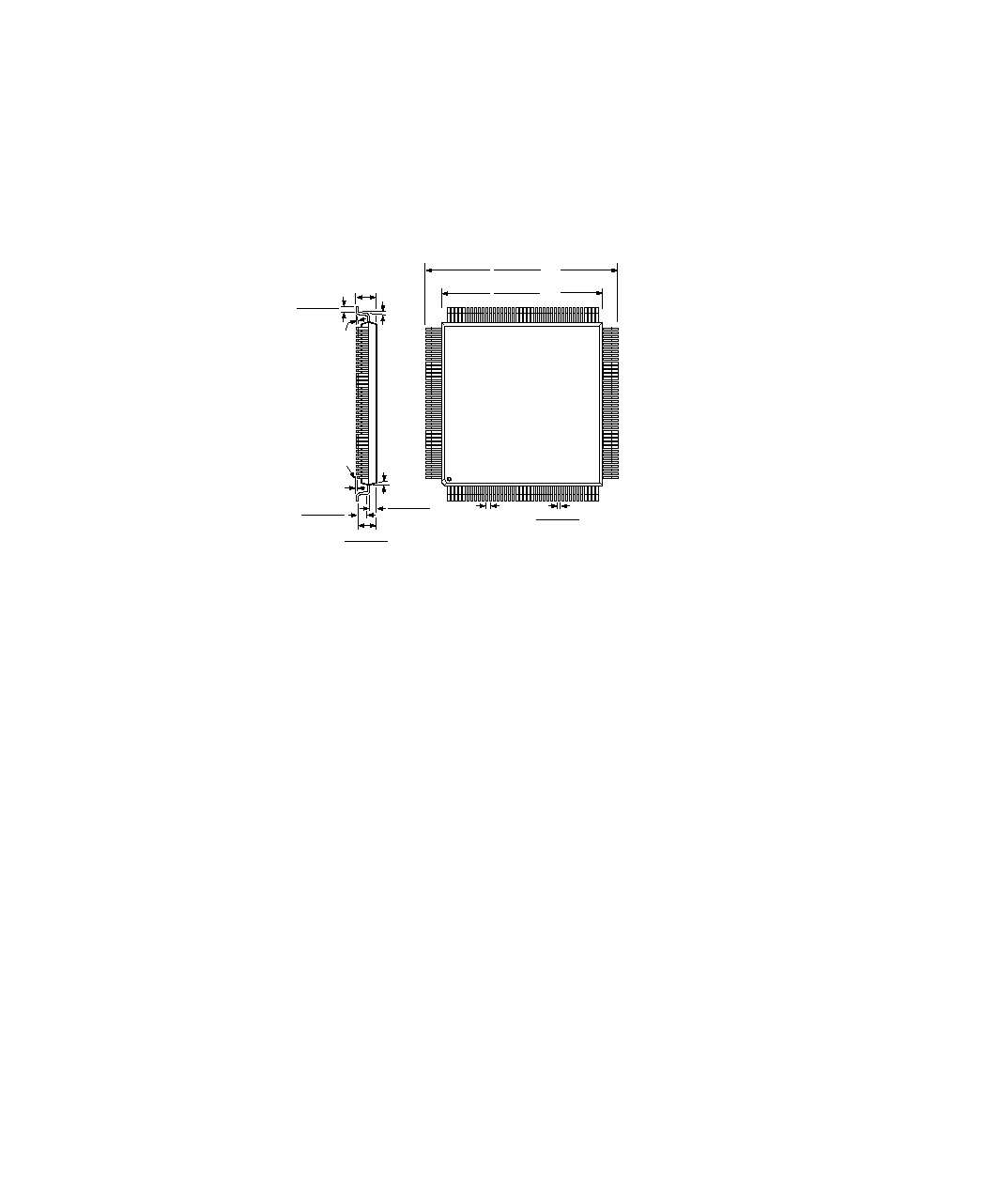
REV. 0
44
ADV7160/ADV7162
OUTLINE DIMENSIONS
Dimensions shown in inches and (mm).
S-160
160-Lead Plastic Quad Flatpack
TOP VIEW
(PINS DOWN)
PIN 1
121
160
1
120
41
40
80
81
0.014 (0.35)
0.011 (0.27)
1.239 (31.45)
1.219 (30.95)
1.107 (28.10)
1.100 (27.90)
SQ
SQ
0.026 (0.65) MIN
SEATING
PLANE
0.160 (4.07)
MAX
0.037 (0.95)
0.026 (0.65)
0.004 (0.10)
MAX
0.145 (3.67)
0.125 (3.17)
0.070 (1.77)
0.062 (1.57)
0.070 (1.77)
0.062 (1.57)
10
°
6
°±
4
°
4
°±
4
°
MAX
PRINTED IN U.S.A.
C201364/95