 | ÐлекÑÑоннÑй компоненÑ: ADV7173 | СкаÑаÑÑ:  PDF PDF  ZIP ZIP |
Äîêóìåíòàöèÿ è îïèñàíèÿ www.docs.chipfind.ru

REV. A
Information furnished by Analog Devices is believed to be accurate and
reliable. However, no responsibility is assumed by Analog Devices for its
use, nor for any infringements of patents or other rights of third parties
which may result from its use. No license is granted by implication or
otherwise under any patent or patent rights of Analog Devices.
a
ADV7172/ADV7173*
One Technology Way, P.O. Box 9106, Norwood, MA 02062-9106, U.S.A.
Tel: 781/329-4700
World Wide Web Site: http://www.analog.com
Fax: 781/326-8703
© Analog Devices, Inc., 1999
Digital PAL/NTSC Video Encoder
with Six DACs (10 Bits), Color Control
and Enhanced Power Management
FEATURES
ITU-R
1
BT601/656 YCrCb to PAL/NTSC Video Encoder
Six High Quality 10-Bit Video DACs
SSAFTM (Super Sub-Alias Filter)
Advanced Power Management Features
PC'98-Compliant (TV Detect with Polling and Auto
Shutdown to Save On Power Consumption)
Low Power DAC Mode
Individual DAC ON/OFF Control
Variable DAC Output Current (5 mA36 mA)
Ultralow Sleep Mode Current
Hue, Brightness, Contrast and Saturation Controls
CGMS (Copy Generation Management System)
WSS (Wide Screen Signalling)
NTSC-M, PAL-M/N, PAL-B/D/G/H/I, PAL-60
YUV Betacam, MII and SMPTE Output Levels
Single 27 MHz Clock Required ( 2 Oversampling)
80 dB Video SNR
32-Bit Direct Digital Synthesizer for Color Subcarrier
Multistandard Video Output Support:
Composite (CVBS)
Component S-Video (Y/C)
Component YUV
EuroSCART RGB
Component YUV + CHROMA + LUMA + CVBS
EuroSCART Output RGB + CHROMA + LUMA + CVBS
Programmable Clamping Output Signal
Advanced Programmable Power-On Reset Sequencing
Video Input Data Port Supports:
CCIR-656 4:2:2 8-Bit Parallel Input Format
SMPTE 170M NTSC-Compatible Composite Video
ITU-R BT.470 PAL-Compatible Composite Video
Luma Sharpness Control
Programmable Luma Filters (Low-Pass [PAL/NTSC],
Notch [PAL/NTSC], Extended [SSAF], CIF and QCIF)
Programmable Chroma Filters (Low-Pass [0.65 MHz,
1.0 MHz, 1.2 MHz and 2.0 MHz], CIF and QCIF)
Programmable VBI (Vertical Blanking Interval)
Programmable Subcarrier Frequency and Phase
Programmable LUMA Delay
CCIR and Square Pixel Operation
Integrated Subcarrier Locking to External Video Source
Color Signal Control/Burst Signal Control
Interlaced/Noninterlaced Operation
Complete On-Chip Video Timing Generator
Programmable Multimode Master/Slave Operation
Macrovision AntiTaping Rev 7.01 (ADV7172 Only)
2
Closed Captioning Support
Teletext Insertion Port (PAL-WST)
On-Board Color Bar Generation
On-Board Voltage Reference
2-Wire Serial MPU Interface (I
2
C
®
Compatible and Fast I
2
C)
Single Supply +5 V or +3.3 V Operation
Small 48-Lead LQFP Package
APPLICATIONS
High Performance DVD Playback Systems, Portable
Video Equipment including Digital Still Cameras and
Laptop PCs, Video Games, PC Video/Multimedia and
Digital Satellite/Cable Systems (Set-Top Boxes/IRD)
NOTES
*This device is protected by U.S. Patent Numbers 4,631,603, 4,577,216, 4,819,098 and other intellectual property rights.
1
ITU-R and CCIR are used interchangeably in this document (ITU-R has replaced CCIR recommendations).
2
The Macrovision anticopy process is licensed for noncommercial home use only, which is its sole intended use in the device. Please contact sales office for latest
Macrovision version available.
SSAF is a trademark of Analog Devices, Inc.
I
2
C is a registered trademark of Philips Corporation.
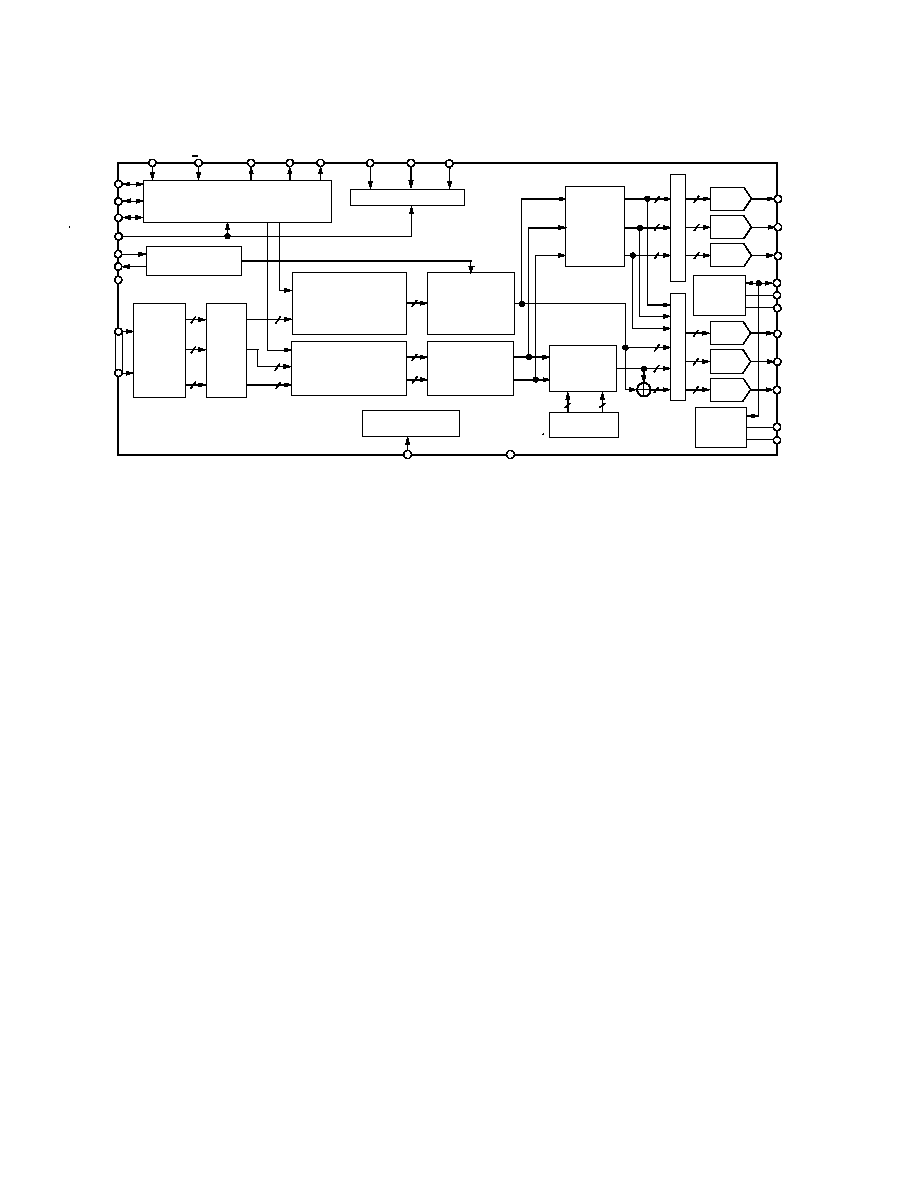
GENERAL DESCRIPTION
The ADV7172/ADV7173 is an integrated Digital Video En-
coder that converts digital CCIR-601 4:2:2 8-bit component
video data into a standard analog baseband television signal
compatible with world wide standards.
There are six DACs available on the ADV7172/ADV7173. In
addition to the Composite output signal there is the facility to
output S-VHS Y/C Video, RGB Video and YUV Video.
The on-board SSAF (Super Sub-Alias Filter), with extended
luminance frequency response and sharp stopband attenuation,
enables studio quality video playback on modern TVs, giving
optimal horizontal line resolution. An additional sharpness
control feature allows extra luminance boost on the frequency
response.
An advanced power management circuit enables optimal control
of power consumption in both normal operating modes and
power down or sleep modes. A PC'98-Compliant autodetect
feature has been added to allow the user to determine whether
or not the DACs are correctly terminated. If not, the ADV7172/
ADV7173 flags that they are not connected through the Status
bit and provides the option of automatically powering them
down, thereby reducing power consumption.
ADV7172/ADV7173
2
REV. A
FUNCTIONAL BLOCK DIAGRAM
8
8
10-BIT
DAC
R
SET1
COMP1
ADV7172/ADV7173
COLOR
DATA
P0
V
REF
R
SET2
COMP2
P7
DAC E
DAC F
DAC D
DAC A
DAC B
DAC C
BRIGHTNESS AND
CONTRAST CONTROL
+
ADD SYNC
+
INTERPOLATOR
10
LUMA
PROGRAMMABLE
FILTER
+
SHARPNESS
FILTER
SATURATION CONTROL
+
ADD BURST
+
INTERPOLATOR
10
PROGRAMMABLE
CHROMA
FILTER
10
8
8
8
REAL-TIME
CONTROL CIRCUIT
SCRESET/RTC
MODULATOR
+
HUE
CONTROL
10
10
10
10
10-BIT
DAC
10
10-BIT
DAC
10
M
U
L
T
I
P
L
E
X
E
R
Y
U
V
8
4:2:2 TO
4:4:4
INTER-
POLATOR
10
10
SIN/COS
DDS BLOCK
DAC
CONTROL
BLOCK
DAC
CONTROL
BLOCK
10-BIT
DAC
10
10
10
10
10-BIT
DAC
10
10-BIT
DAC
10
M
U
L
T
I
P
L
E
X
E
R
YUV TO
RBG
MATRIX
+
YUV
LEVEL
CONTROL
BLOCK
I
2
C MPU PORT
HSYNC
FIELD/
VSYNC
BLANK
TTX
TTXREQ
V
AA
RESET
TELETEXT
INSERTION BLOCK
YCrCb
TO
YUV
MATRIX
CLOCK
CSO_HSO VSO
CLAMP
SCLOCK SDATA
ALSB
VIDEO TIMING
GENERATOR
GND
PAL NTSC
The ADV7172/ADV7173 also supports both PAL and NTSC
square pixel operation. The parts also incorporate WSS and
CGMS-A data control generation.
The ADV7172/ADV7173 is designed with four color controls
(hue, contrast, brightness and saturation). All YUV formats
(SMPTE, MII and Betacam) are supported in both PAL and
NTSC.
The output video frames are synchronized with the incoming
data Timing Reference Codes. Optionally the encoder accepts
(and can generate)
HSYNC , VSYNC and FIELD timing
signals. These timing signals can be adjusted to change pulse-
width and position while the part is in the master mode. The
Encoder requires a single two times pixel rate (27 MHz) clock
for standard operation. Alternatively the Encoder requires a
24.54 MHz clock for NTSC or 29.5 MHz clock for PAL square
pixel mode operation. All internal timing is generated on-chip.
HSO/CSO and VSO TTL outputs, synchronous to the analog
output video, are also available. A programmable CLAMP
output signal is also available to enable clamping in either the
front or back porch of the video signal.
A separate teletext port enables the user to directly input tele-
text data during the vertical blanking interval.
The ADV7172/ADV7173 modes are set up over a two wire
serial bidirectional port (I
2
C-Compatible) with two slave ad-
dresses. Functionally the ADV7173 and ADV7172 are the same
with the exception that the ADV7172 can output the Macrovi-
sion anticopy algorithm.
The ADV7172/ADV7173 is packaged in a 48-lead LQFP pack-
age (1.4 mm thickness).
DATA PATH DESCRIPTION
For PAL B, D, G, H, I, M, N and NTSC M, N modes, YCrCb
4:2:2 Data is input via the CCIR-656-Compatible Pixel Port at
a 27 MHz Data Rate. The Pixel Data is demultiplexed to form
three data paths. Y typically has a range of 16 to 235, Cr and
Cb typically have a range of 128
±
112; however, it is possible
to input data from 1 to 254 on both Y, Cb and Cr. The ADV7172/
ADV7173 supports PAL (B, D, G, H, I, N, M) and NTSC
(with and without pedestal) standards. The Y data is then ma-
nipulated by being scaled for contrast control and a setup level
is added for brightness control. The Cr, Cb data is also scaled
and saturation control is added. The appropriate Sync, Blank
and Burst levels are then added to the YCrCb data. Macrovi-
sion AntiTaping (ADV7172 only), Closed-Captioning and
Teletext levels are also added to Y, and the resultant data is
interpolated to a rate of 27 MHz. The interpolated data is fil-
tered and scaled by three digital FIR Filters.
The U and V Signals are modulated by the appropriate sub-
carrier sine/cosine phases and a phase offset may be added onto
the color subcarrier during active video to allow hue adjustment.
The resulting U and V signals are then added together to make
up the chrominance signal. The luma (Y) signal can be delayed
13 luma cycles (each cycle is 74 ns) with respect to the chroma
signal. The luma and chroma signals are then added together to
make up the composite video signal. All edges are slew rate
limited.
The YCrCb data is also used to generate RGB data with appro-
priate Sync and Blank levels. The YUV levels are also scaled to
output the suitable SMPTE or Betacam levels.
There are six DACs on the ADV7172/ADV7173. Three of these
DACs are capable of providing 34.66 mA of current. The other
three DACs provide 8.66 mA each.
The six l0-bit DACs can be used to output:
1. Composite Video + RGB Video + LUMA + CHROMA.
2. Composite Video + YUV Video + LUMA + CHROMA.
Alternatively, each DAC can be individually powered off if not
required. A complete description of DAC output configurations
is given in Appendix 8.
Video output levels are illustrated in Appendix 6.
(continued on page 11)
3
REV. A
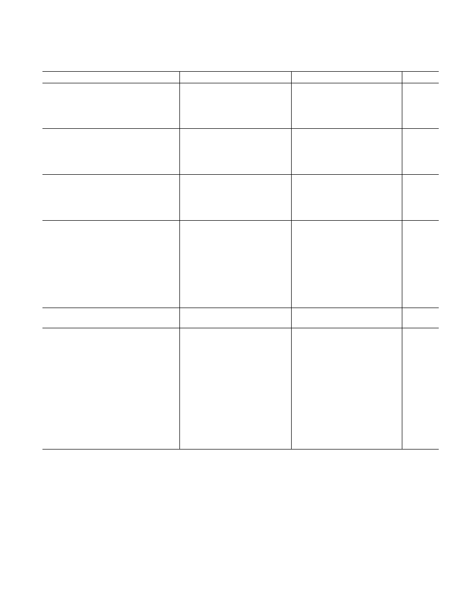
ADV7172/ADV7173
(V
AA
= +5 V 5%
1
, V
REF
= 1.235 V, R
SET1,2
= 600
unless otherwise noted. All specifications T
MIN
to T
MAX
2
unless otherwise noted)
Parameter
Test Conditions
1
Min
Typ
Max
Units
STATIC PERFORMANCE
Resolution (Each DAC)
10
Bits
Accuracy (Each DAC)
Integral Nonlinearity
3
±
1.0
LSB
Differential Nonlinearity
3
Guaranteed Monotonic
±
1.0
LSB
DIGITAL INPUTS
Input High Voltage, V
INH
2
V
Input Low Voltage, V
INL
0.8
V
Input Current, I
IN
V
IN
= 0.4 V or 2.4 V
±
1
µ
A
Input Capacitance, C
IN
10
pF
DIGITAL OUTPUTS
Output High Voltage, V
OH
I
SOURCE
= 400
µ
A
2.4
V
Output Low Voltage, V
OL
I
SINK
= 3.2 mA
0.4
V
Three-State Leakage Current
10
µ
A
Three-State Output Capacitance
10
pF
ANALOG OUTPUTS
Output Current (DACs A, B, C)
4
R
SET1
= 150
, R
L
= 37.5
33
34.7
37
mA
Output Current (DACs A, B, C)
5
R
SET1
= 1041
, R
L
= 262.5
5
mA
Output Current (DACs D, E, F)
6
R
SET2
= 600
, R
L
= 150
8.25
8.66
9.25
mA
Output Current (DACs D, E, F)
5
R
SET2
= 1041
, R
L
= 262.5
5
mA
DAC-to-DAC Matching (DACs A, B, C)
7
1
4.0
%
DAC-to-DAC Matching (DACs D, E, F)
7
1
4.0
%
Output Compliance, V
OC
0
+1.4
V
Output Impedance, R
OUT
30
k
Output Capacitance, C
OUT
I
OUT
= 0 mA
30
pF
VOLTAGE REFERENCE
Reference Range, V
REF
I
VREFOUT
= 20
µ
A
1.112
1.235
1.359
V
POWER REQUIREMENTS
V
AA
4.75
5.0
5.25
V
Normal Power Mode
I
DAC
(max)
8, 9
R
SET1,2
= 600
59
65
mA
I
DAC
(min)
8, 9
R
SET1,2
= 1041
30
mA
I
CCT
10
78
90
mA
Low Power Mode
I
DAC
(max)
11
R
SET1
= 150
64
mA
I
DAC
(min)
11
15
mA
I
CCT
10
78
90
mA
Sleep Mode
I
DAC
12
0.1
µ
A
I
CCT
13
0.1
µ
A
Power Supply Rejection Ratio
COMP = 0.1
µ
F
0.01
0.5
%/%
NOTES
1
The max/min specifications are guaranteed over this range. The max/min values are typical over 4.75 V to 5.25 V.
2
Temperature range T
MIN
to T
MAX
: 0
°
C to +70
°
C.
3
Characterized by design.
4
Full
drive into 75
doubly terminated load.
5
Minimum drive current (used with buffered/scaled output load).
6
Full drive into 150
load.
7
Specification guaranteed by characterization.
8
I
DAC
is the total current ("min" corresponds to 5 mA output per DAC, "max" corresponds to 8.66 mA output per DAC ) to drive DACs A, B, C, D, E, F. Turning off
individual DACs reduces I
DAC
correspondingly, also DACs A, B, C can be configured to output a max current of 37 mA but DAC D, E, F must be turned off.
9
All six DACs on (DAC A, B, C, D, E, F).
10
I
CCT
(Circuit Current) is the continuous current required to drive the device.
11
Only large DACs (DACs A, B, C) on per low power mode.
12
Total DAC current in Sleep Mode.
13
Total continuous current during Sleep Mode.
Specifications subject to change without notice.
5 V SPECIFICATIONS
SPECIFICATIONS

4
REV. A
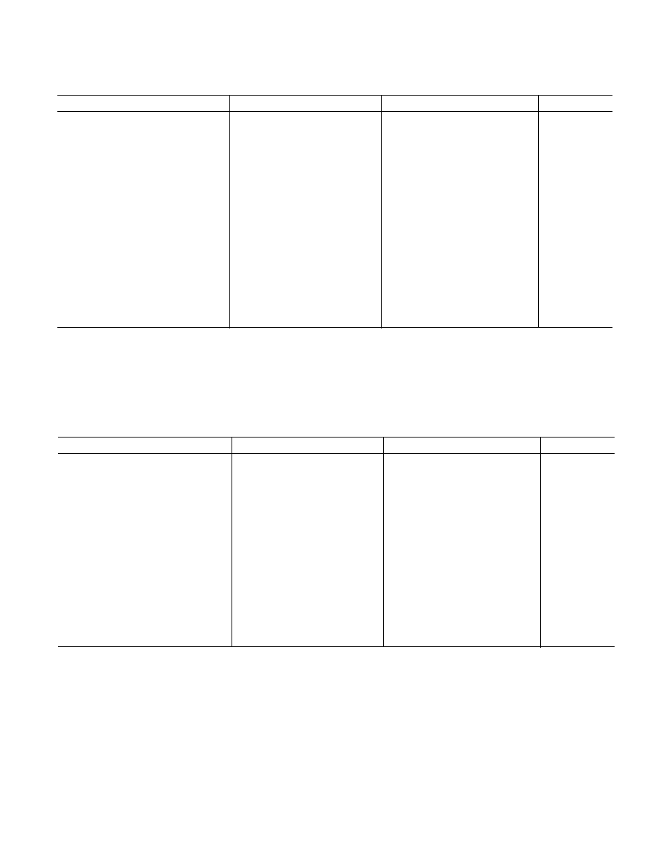
ADV7172/ADV7173SPECIFICATIONS
Parameter
Test Conditions
1
Min
Typ
Max
Units
STATIC PERFORMANCE
3
Resolution (Each DAC)
10
Bits
Accuracy (Each DAC)
Integral Nonlinearity
1.0
LSB
Differential Nonlinearity
Guaranteed Monotonic
1.0
LSB
DIGITAL INPUTS
3
Input High Voltage, V
INH
2
V
Input Low Voltage, V
INL
0.8
V
Input Current, I
IN
V
IN
= 0.4 V or 2.4 V
±
1
µ
A
Input Capacitance, C
IN
10
pF
DIGITAL OUTPUTS
3
Output High Voltage, V
OH
I
SOURCE
= 400
µ
A
2.4
V
Output Low Voltage, V
OL
I
SINK
= 3.2 mA
0.4
V
Three-State Leakage Current
10
µ
A
Three-State Output Capacitance
10
pF
ANALOG OUTPUTS
3
Output Current (DACs A, B, C)
4
R
SET1
= 150
, R
L
= 37.5
34.7
mA
Output Current (DACs A, B, C)
5
R
SET1
= 1041
, R
L
= 262.5
5
mA
Output Current (DACs D, E, F)
6
R
SET2
= 600
, R
L
= 150
8.66
mA
Output Current (DACs D, E, F)
5
R
SET2
= 1041
, R
L
= 262.5
5
mA
DAC-to-DAC Matching (DACs A, B, C)
3
1
4.0
%
DAC-to-DAC Matching (DACs D, E, F)
3
1
4.0
%
Output Compliance, V
OC
+1.4
V
Output Impedance, R
OUT
30
k
Output Capacitance, C
OUT
I
OUT
= 0 mA
30
pF
POWER REQUIREMENTS
3, 7
V
AA
3.0
3.3
3.6
V
Normal Power Mode
I
DAC
(max)
8, 9
R
SET1,2
= 600
58
65
mA
I
DAC
(min)
8
R
SET1,2
= 1041
30
mA
I
CCT
10
40
mA
Sleep Mode
I
DAC
11
0.1
µ
A
I
CCT
12
0.1
µ
A
Power Supply Rejection Ratio
COMP = 0.1
µ
F
0.01
%/%
NOTES
1
The max/min specifications are guaranteed over this range. The max/min values are typical over 3.0 V to 3.6 V.
2
Temperature range T
MIN
to T
MAX
: 0
°
C to +70
°
C.
3
Guaranteed by characterization.
4
Full
drive into 75
doubly terminated load.
5
Minimum drive current (used with buffered/scaled output load).
6
Full Drive into 150
load.
7
Power measurements are taken with Clock Frequency = 27 MHz. Max T
J
= 110
°
C.
8
I
DAC
is the total current ("min" corresponds to 5 mA output per DAC, "max" corresponds to 8.66 mA output per DAC ) to drive DACs A, B, C, D, E, F. Turning off
individual DACs reduces I
DAC
correspondingly, also DACs A, B, C can be configured to output a max current of 37 mA.
9
DACs A, B, C can output 35 mA typically at 3.3 V (R
SET
= 150
and R
L
= 37.5
), optimum performance obtained at 18 mA DAC Current (R
SET
= 300
and
R
L
= 75
).
10
I
CCT
(Circuit Current) is the continuous current required to drive the device.
11
Total DAC current in Sleep Mode.
12
Total continuous current during Sleep Mode.
Specifications subject to change without notice.
3.3 V SPECIFICATIONS
(V
AA
= +3.0 V3.6 V
1
, V
REF
= 1.235 V, R
SET1,2
= 600
unless otherwise noted. All specifications T
MIN
to T
MAX
2
unless otherwise noted)
5
REV. A
ADV7172/ADV7173
Parameter
Conditions
1
Min
Typ
Max
Units
Differential Gain
3, 4
Normal Power Mode
0.3
0.7
%
Differential Phase
3, 4
Normal Power Mode
0.4
0.7
Degrees
Differential Gain
3, 4
Lower Power Mode
0.5
1.0
%
Differential Phase
3, 4
Lower Power Mode
2.0
3.0
Degrees
SNR
3, 4
(Pedestal)
RMS
75
dB rms
SNR
3, 4
(Pedestal)
Peak Periodic
66
dB p-p
SNR
3, 4
(Ramp)
RMS
60
dB rms
SNR
3, 4
(Ramp)
Peak Periodic
58
dB p-p
Hue Accuracy
3, 4
0.7
Degrees
Color Saturation Accuracy
3, 4
0.9
%
Chroma Nonlinear Gain
3, 4
Referenced to 40 IRE
1.2
±
%
Chroma Nonlinear Phase
3, 4
0.3
0.5
±
Degrees
Chroma/Luma Intermod
3, 4
0.2
0.4
±
%
Chroma/Luma Gain Inequality
3, 4
1.0
±
%
Chroma/Luma Delay Inequality
3, 4
0.5
ns
Luminance Nonlinearity
3, 4
1.0
1.7
±
%
Chroma AM Noise
3, 4
79
82
dB
Chroma PM Noise
3, 4
79
80
dB
NOTES
1
The max/min specifications are guaranteed over this range. The max/min values are typical over 4.75 V to 5.25 V range.
2
Temperature range T
MIN
to T
MAX
: 0
°
C to +70
°
C.
3
These specifications are for the low-pass filter only and guaranteed by design.
4
Guaranteed by characterization.
Specifications subject to change without notice.
5 V DYNAMIC SPECIFICATIONS
(V
AA
= +5 V 5%
1
, V
REF
= 1.235 V, R
SET1,2
= 600
unless otherwise noted. All
specifications T
MIN
to T
MAX
2
unless otherwise noted.)
Parameter
Conditions
1
Min
Typ
Max
Units
Differential Gain
3
Normal Power Mode
0.6
%
Differential Phase
3
Normal Power Mode
0.5
Degrees
Differential Gain
3
Lower Power Mode
1.0
%
Differential Phase
3
Lower Power Mode
0.5
Degrees
SNR
3
(Pedestal)
RMS
75
dB rms
SNR
3
(Pedestal)
Peak Periodic
70
dB p-p
SNR
3
(Ramp)
RMS
60
dB rms
SNR
3
(Ramp)
Peak Periodic
58
dB p-p
Hue Accuracy
3
1.0
Degrees
Color Saturation Accuracy
3
1.0
%
Luminance Nonlinearity
3
1.1
±
%
Chroma AM Noise
3
83
dB
Chroma PM Noise
3
79
dB
Chroma Nonlinear Gain
3, 4
Referenced to 40 IRE
1.2
±
%
Chroma Nonlinear Phase
3, 4
0.3
±
Degrees
Chroma/Luma Intermod
3, 4
0.2
±
%
NOTES
1
The max/min specification are guaranteed over this range. The max with values are typical over a 3.0 V to 3.6 V range.
2
Temperature range T
MIN
to T
MAX
: 0
°
C to +70
°
C.
3
Guaranteed by characterization.
4
These specifications are for the low-pass filter only and guaranteed by design.
Specifications subject to change without notice.
3.3 V DYNAMIC SPECIFICATIONS
(V
AA
= +3.0 V 3.6 V
1
, V
REF
= 1.235 V, R
SET1,2
= 600
unless otherwise noted. All
specifications T
MIN
to T
MAX
2
unless otherwise noted.)