Äîêóìåíòàöèÿ è îïèñàíèÿ www.docs.chipfind.ru
Chip Scale PAL/NTSC Video Encoder with
Advanced Power Management
ADV7174/ADV7179
Rev. A
Information furnished by Analog Devices is believed to be accurate and reliable.
However, no responsibility is assumed by Analog Devices for its use, nor for any
infringements of patents or other rights of third parties that may result from its use.
Specifications subject to change without notice. No license is granted by implication
or otherwise under any patent or patent rights of Analog Devices. Trademarks and
registered trademarks are the property of their respective owners.
One Technology Way, P.O. Box 9106, Norwood, MA 02062-9106, U.S.A.
Tel: 781.329.4700
www.analog.com
Fax: 781.326.8703
© 2004 Analog Devices, Inc. All rights reserved.
FEATURES
ITU-R
1
BT601/BT656 YCrCb to PAL/NTSC video encoder
High quality 10-bit video DACs
SSAFTM (super sub-alias filter)
Advanced power management features
CGMS (copy generation management system)
WSS (wide screen signaling)
NTSC M, PAL N
2
, PAL B/D/G/H/I, PAL-M
3
, PAL 60
Single 27 MHz clock required (×2 oversampling)
Macrovision 7.1 (ADV7174 only)
80 dB video SNR
32-bit direct digital synthesizer for color subcarrier
Multistandard video output support:
Composite (CVBS)
Component S-video (Y/C)
Video input data port supports:
CCIR-656 4:2:2 8-bit parallel input format
Programmable simultaneous composite and S-video or RGB
(SCART)/YPbPr video outputs
Programmable luma filters low-pass [PAL/NTSC] notch,
extended SSAF, CIF, and QCIF
Programmable chroma filters (low-pass [0.65 MHz, 1.0 MHz,
1.2 MHz, and 2.0 MHz], CIF, and QCIF)
Programmable VBI (vertical blanking interval)
Programmable subcarrier frequency and phase
Programmable LUMA delay
Individual on/off control of each DAC
CCIR and square pixel operation
Integrated subcarrier locking to external video source
Color signal control/burst signal control
Interlaced/noninterlaced operation
Complete on-chip video timing generator
Programmable multimode master/slave operation
Closed captioning support
Teletext insertion port (PAL-WST)
On-board color bar generation
On-board voltage reference
2-wire serial MPU interface (I
2
C® compatible and fast I
2
C)
Single-supply 2.8 V and 3.3 V operation
Small 40-lead 6 mm × 6 mm LFCSP package
-40°C to +85°C at 3.3 V
-20°C to +85°C at 2.8 V
APPLICATIONS
Portable video applications
Mobile phones
Digital still cameras
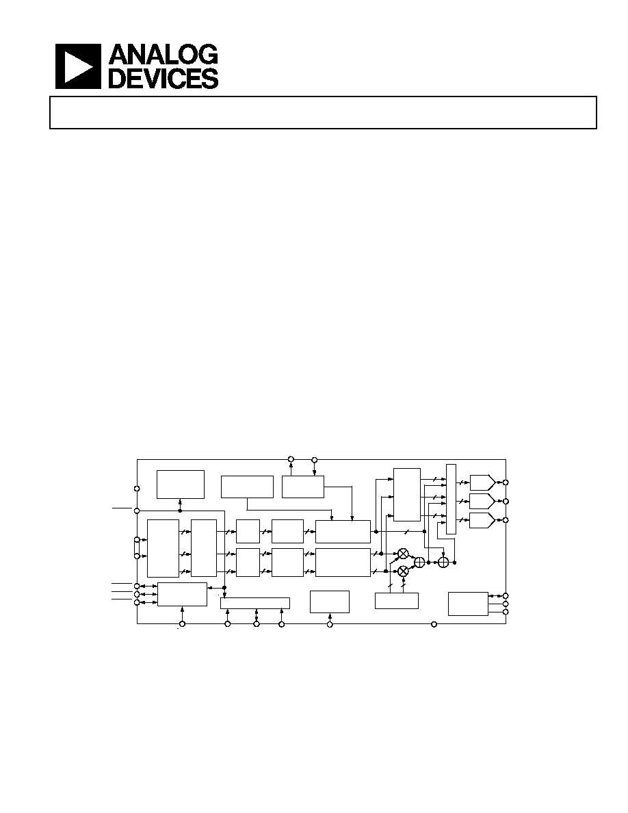
FUNCTIONAL BLOCK DIAGRAM
9
9
8
10
8
8
8
10
8
8
8
10
10
10
10
10
10
I
2
C MPU PORT
SCLOCK
SDATA
ALSB
HSYNC
FIELD/VSYNC
BLANK
CLOCK
GND
DAC A (PIN 29)
V
REF
R
SET
COMP
8
8
8
ADV7174/ADV7179
COLOR
DATA
P7P0
SCRESET/RTC
DAC B (PIN 28)
DAC C (PIN 24)
V
AA
Y
U
V
RESET
TELETEXT
INSERTION
BLOCK
YUV TO
RBG
MATRIX
VOLTAGE
REFERENCE
CIRCUIT
REAL-TIME
CONTROL
CIRCUIT
10-BIT
DAC
10-BIT
DAC
10-BIT
DAC
M
U
L
T
I
P
L
E
X
E
R
CGMS AND WSS
INSERTION
BLOCK
ADD
SYNC
ADD
BURST
INTER-
POLATOR
SIN/COS
DDS BLOCK
VIDEO TIMING
GENERATOR
PROGRAMMABLE
LUMINANCE
FILTER
PROGRAMMABLE
CHROMINANCE
FILTER
INTER-
POLATOR
POWER
MANAGEMENT
CONTROL
(SLEEP MODE)
YCrCb
TO
YUV
MATRIX
4:2:2 TO
4:4:4
INTER-
POLATOR
TTXREQ TTX
10
10
10
U
V
02980-A-001
Figure 1.
1
ITU-R and CCIR are used interchangeably in this document (ITU-R has replaced CCIR recommendations).
2
Throughout the document, N is referenced to PAL Combination N.
3
ADV7174 only.
Protected by U.S. Patent Numbers 5,343,196 and 5,442,355 and other intellectual property rights.
Protected by U.S. Patent Numbers 4,631,603, 4,577,216, 4,819,098 and other intellectual property rights. The Macrovision anticopy process is licensed for
noncommercial home use only, which is its sole intended use in the device. Contact the sales office for the latest Macrovision version available.

ADV7174/ADV7179
Rev. A | Page 2 of 52
TABLE OF CONTENTS
Specifications..................................................................................... 4
2.8 V Specifications ...................................................................... 4
2.8 V Timing Specifications ........................................................ 5
3.3 V Specifications ...................................................................... 6
3.3 V Timing Specifications ........................................................ 7
Absolute Maximum Ratings............................................................ 9
ESD Caution.................................................................................. 9
Pin Configuration and Function Descriptions........................... 10
General Description ....................................................................... 11
Data Path Description................................................................ 11
Internal Filter Response............................................................. 11
Typical Performance Characteristics ........................................... 13
Features ............................................................................................ 16
Color Bar Generation ................................................................ 16
Square Pixel Mode...................................................................... 16
Color Signal Control .................................................................. 16
Burst Signal Control................................................................... 16
NTSC Pedestal Control ............................................................. 16
Pixel Timing Description .......................................................... 16
8-Bit YCrCb Mode ................................................................. 16
Subcarrier Reset.......................................................................... 16
Real-Time Control ..................................................................... 16
Video Timing Description .................................................... 16
Vertical Blanking Data Insertion.......................................... 17
Mode 0 (CCIR-656): Slave Option....................................... 17
Mode 0 (CCIR-656): Master Option ................................... 17
Mode 1: Slave Option HSYNC, BLANK, FIELD................ 20
Mode 1: Master Option HSYNC, BLANK, FIELD ............ 21
Mode 2: Slave Option HSYNC, VSYNC, BLANK.............. 22
Mode 2: Master Option HSYNC, VSYNC, BLANK .......... 23
Mode 3: Master/Slave Option HSYNC, BLANK, FIELD.. 24
Power-On Reset.......................................................................... 25
SCH Phase Mode........................................................................ 25
MPU Port Description............................................................... 25
Register Accesses ........................................................................ 26
Register Programming................................................................... 27
Subaddress Register (SR7SR0) ............................................... 27
Register Select (SR5SR0) ......................................................... 27
Mode Register 1 (MR1) ............................................................. 29
Mode Register 2 (MR2) ............................................................. 30
Mode Register 3 (MR3) ............................................................. 31
Mode Register 4 (MR4) ............................................................. 32
Timing Mode Register 0 (TR0) ................................................ 33
Timing Mode Register 1 (TR1) ................................................ 34
Subcarrier Frequency Registers 30 ........................................ 35
Subcarrier Phase Register.......................................................... 35
Closed Captioning Even Field Data Registers 10 ................ 35
Closed Captioning Odd Field Data Registers 10 ................. 36
NTSC Pedestal/PAL Teletext Control Registers 30 ............. 36
Teletext Request Control Register (TC07) .............................. 37
CGMS_WSS Register 0 (C/W0)............................................... 37
CGMS_WSS Register 1 (C/W1)............................................... 38
CGMS_WSS Register 2 (C/W2)............................................... 38
Appendix 1--Board Design and Layout Considerations.......... 39
Ground Planes ............................................................................ 39
Power Planes ............................................................................... 39
Supply Decoupling ..................................................................... 40
Digital Signal Interconnect ....................................................... 40
Analog Signal Interconnect....................................................... 40
Appendix 2--Closed Captioning ................................................. 41

ADV7174/ADV7179
Rev. A | Page 3 of 52
Appendix 3--Copy Generation Management System (CGMS)
............................................................................................................42
Function of CGMS Bits ..............................................................42
Appendix 4--Wide Screen Signaling (WSS) ...............................43
Function of WSS Bits ..................................................................43
Appendix 5--Teletext .....................................................................44
Teletext Insertion.........................................................................44
Teletext Protocol..........................................................................44
Appendix 6--Waveforms ...............................................................45
NTSC Waveforms (with Pedestal) ............................................45
NTSC Waveforms (without Pedestal) ......................................46
PAL Waveforms ...........................................................................47
Pb Pr Waveforms.........................................................................48
Appendix 7--Optional Output Filter ...........................................49
Appendix 8--Recommended Register Values.............................50
Outline Dimensions........................................................................52
Ordering Guide ...........................................................................52
REVISION HISTORY
2/04--Changed from REV. 0 to REV A.
Added 2.8 V Version .......................................................... Universal
Format Updated.................................................................. Universal
Device Currents Updated on 3.3 V Specification .......... Universal
Added new Table 1 and
Renumbered Subsequent Tables.............4
Added new Table 2 and Renumbered Subsequent Tables ...........5
Change to Figure 54 ........................................................................38
Change to Figure 55 ........................................................................39
Change to Figure 79 ........................................................................48
Changed Ordering Guide Temperature Specifications ..............52
Updated Outline Dimensions........................................................52
10/02--Revision 0: Initial Version

ADV7174/ADV7179
Rev. A | Page 4 of 52
SPECIFICATIONS
2.8 V SPECIFICATIONS
V
AA
= 2.8 V, V
REF
= 1.235 V, R
SET
= 150 . All specifications T
MIN
to T
MAX
1
, unless otherwise noted.
Table 1.
Parameter
Conditions
1
Min
Typ
Max
Unit
STATIC PERFORMANCE
2
Resolution (Each DAC)
10
Bits
Accuracy (Each DAC)
Integral Nonlinearity
R
SET
= 300
±3.0
LSB
Differential Nonlinearity
Guaranteed monotonic
±1
LSB
DIGITAL INPUTS
2
Input High Voltage, V
INH
1.6
V
Input Low Voltage, V
INL
0.7
V
Input Current, I
IN
V
IN
= 0.4 V or 2.4 V
±1
µA
Input Capacitance, C
IN
10
pF
DIGITAL OUTPUTS
2
Output High Voltage, V
OH
I
SOURCE
= 400 µA
2.4
V
Output Low Voltage, V
OL
I
SINK
= 3.2 mA
0.4
V
Three-State Leakage Current
10
µA
Three-State Output Capacitance
10
pF
ANALOG OUTPUTS
2
Output Current
3
R
SET
= 150 , R
L
= 37.5
33
34.7
37
mA
DAC-to-DAC Matching
2.0
%
Output Compliance, V
OC
0
1.4
V
Output Impedance, R
OUT
30
k
Output Capacitance, C
OUT
I
OUT
= 0 mA
30
pF
POWER REQUIREMENTS
2, 4
V
AA
2.8
V
Normal Power Mode
I
DAC
(Max)
5
R
SET
= 150 , R
L
= 37.5
115
120
mA
I
CCT
6
30
mA
Low Power Mode
I
DAC
(Max)
5
62
mA
I
CCT
6
30
mA
Sleep Mode
I
DAC
7
0.1
µA
I
CCT
8
0.001
µA
Power Supply Rejection Ratio
COMP = 0.1 µF
0.01
0.5
%/%
1
Temperature range T
MIN
to T
MAX
: 20°C to +85°C.
2
Guaranteed by characterization.
3
DACs can output 35 mA typically at 2.8 V (R
SET
= 150 and R
L
= 37.5 ). Full drive into 37.5 load.
4
Power measurements are taken with clock frequency = 27 MHz. Max T
J
= 110°C.
5
I
DAC
is the total current (min corresponds to 5 mA output per DAC, max corresponds to 37 mA output per DAC) to drive all three DACs. Turning off individual DACs
reduces I
DAC
correspondingly.
6
I
CCT
(circuit current) is the continuous current required to drive the device.
7
Total DAC current in sleep mode.
8
Total continuous current during sleep mode.

ADV7174/ADV7179
Rev. A | Page 5 of 52
2.8 V TIMING SPECIFICATIONS
V
AA
= 2.8 V, V
REF
= 1.235 V, R
SET
= 150 . All specifications T
MIN
to T
MAX
1
, unless otherwise noted.
Table 2.
Parameter
Conditions
1
Min
Typ
Max
Unit
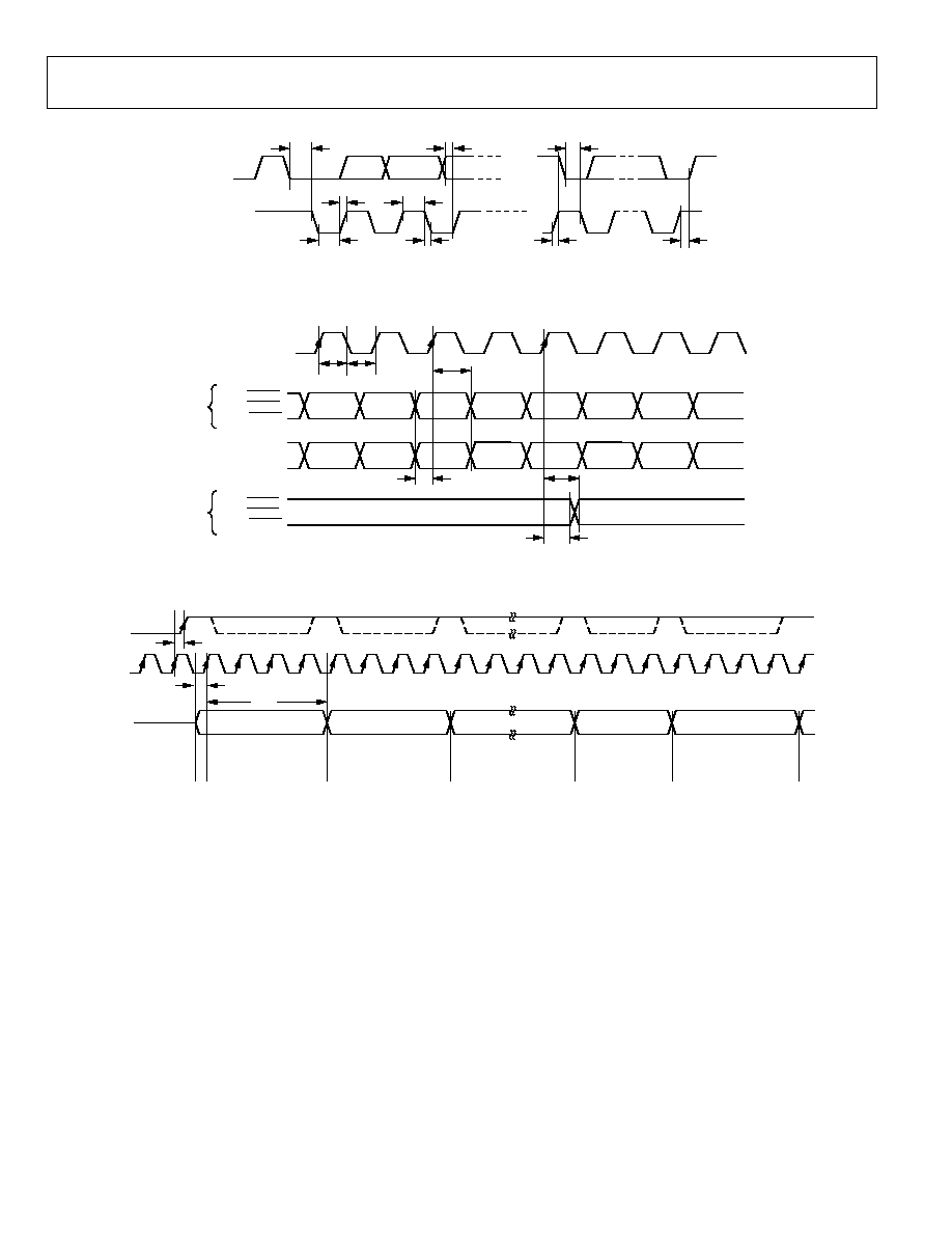
MPU PORT
2, 3
SCLOCK Frequency
0
400
kHz
SCLOCK High Pulse Width, t
1
0.6
µs
SCLOCK Low Pulse Width, t
2
1.3
µs
Hold Time (Start Condition), t
3
After this period the first clock is generated
0.6
µs
Setup Time (Start Condition), t
4
Relevant for repeated start condition
0.6
µs
Data Setup Time, t
5
100
ns
SDATA, SCLOCK Rise Time, t
6
300
ns
SDATA, SCLOCK Fall Time, t
7
300
ns
Setup Time (Stop Condition), t
8
0.6
µs
ANALOG OUTPUTS
3, 4
Analog Output Delay
7
ns
DAC Analog Output Skew
0
ns
CLOCK CONTROL AND PIXEL PORT
4, 5
f
CLOCK
27
MHz
Clock High Time, t
9
8
ns
Clock Low Time, t
10
8
ns
Data Setup Time, t
11
3.5
ns
Data Hold Time, t
12
4
ns
Control Setup Time, t
11
4
ns
Control Hold Time, t
12
3
ns
Digital Output Access Time, t
13
12
ns
Digital Output Hold Time, t
1
4
8
ns
Pipeline Delay, t
PD
5
48
Clock Cycles
TELETEXT
3, 4, 6
Digital Output Access Time, t
16
23
ns
Data Setup Time, t
17
2
ns
Data Hold Time, t
18
6
ns
RESET CONTROL
3, 4
RESET Low Time
6
ns
1
Temperature range T
MIN
to T
MAX
: 20°C to +85°C.
2
TTL input values are 0 V to 2.8 V, with input rise/fall times -3 ns, measured between the 10% and 90% points. Timing reference points at 50% for inputs and outputs.
Analog output load 10 pF.
3
Guaranteed by characterization.
4
Output delay measured from the 50% point of the rising edge of CLOCK to the 50% point of full-scale transition.
5
See Figure 60.
6
Teletext Port consists of the following:
Teletext Output: TTXREQ
Teletext Input: TTX

ADV7174/ADV7179
Rev. A | Page 6 of 52
3.3 V SPECIFICATIONS
V
AA
= 3.0 V3.6 V
1
, V
REF
= 1.235 V, R
SET
= 150 . All specifications T
MIN
to T
MAX
2
, unless otherwise noted.
Table 3.
Parameter
Conditions
1
Min
Typ
Max
Unit
STATIC PERFORMANCE
3
Resolution (Each DAC)
10
Bits
Accuracy (Each DAC)
Integral Nonlinearity
R
SET
= 300
± 0.6
LSB
Differential Nonlinearity
Guaranteed Monotonic
± 1
LSB
DIGITAL INPUTS
3
Input High Voltage, V
INH
2
V
Input Low Voltage, V
INL
0.8
V
Input Current, I
IN
3, 4
V
IN
= 0.4 V or 2.4 V
± 1
µA
Input Capacitance, C
IN
10
pF
DIGITAL OUTPUTS
3
Output High Voltage, V
OH
I
SOURCE
= 400 µA
2.4
V
Output Low Voltage, V
OL
I
SINK
= 3.2 mA
0.4
V
Three-State Leakage Current
10
µA
Three-State Output Capacitance
10
pF
ANALOG OUTPUTS
3
Output Current
4, 5
R
SET
= 150 , R
L
= 37.5
33
34.7
37
mA
Output Current
6
R
SET
= 1041 , R
L
= 262.5
5
mA
DAC-to-DAC Matching
2.0
%
Output Compliance, V
OC
0
1.4
V
Output Impedance, R
OUT
30
k
Output Capacitance, C
OUT
I
OUT
= 0 mA
30
pF
POWER REQUIREMENTS
3, 7
V
AA
3.0
3.3
3.6
V
Normal Power Mode
I
DAC
(Max)
8
R
SET
= 150 , R
L
= 37.5
115
120
mA
I
DAC
(Min)
8
R
SET
= 1041 , R
L
= 262.5
20
mA
I
CCT
9
35
mA
Low Power Mode
I
DAC
(Max)
8
62
mA
I
DAC
(Min)
8
20
mA
I
CCT
9
35
mA
Sleep Mode
I
DAC
10
0.1
µA
I
CCT
11
0.001
µA
Power Supply Rejection Ratio
COMP = 0.1 µF
0.01
0.5
%/%
1
The max/min specifications are guaranteed over this range. The max/min values are typical over 3.0 V to 3.6 V.
2
Temperature range T
MIN
to T
MAX
: 40°C to +85°C.
3
Guaranteed by characterization.
4
Full drive into 37.5 load.
5
DACs can output 35 mA typically at 3.3 V (R
SET
= 150 and R
L
= 37.5 ), optimum performance obtained at 18 mA DAC current (R
SET
= 300 and R
L
= 75 ).
6
Minimum drive current (used with buffered/scaled output load).
7
Power measurements are taken with clock frequency = 27 MHz. Max T
J
= 110°C.
8
I
DAC
is the total current (min corresponds to 5 mA output per DAC, max corresponds to 37 mA output per DAC) to drive all three DACs. Turning off individual DACs
reduces I
DAC
correspondingly.
9
I
CCT
(circuit current) is the continuous current required to drive the device.
10
Total DAC current in sleep mode.
11
Total continuous current during sleep mode.

ADV7174/ADV7179
Rev. A | Page 7 of 52
3.3 V TIMING SPECIFICATIONS
V
AA
= 3.0 V3.6 V
1
, V
REF
= 1.235 V, R
SET
= 150 . All specifications T
MIN
to T
MAX
2
, unless otherwise noted.
Table 4.
Parameter
Conditions
1
Min
Typ
Max
Unit
MPU PORT
3, 4
SCLOCK Frequency
0
400
kHz
SCLOCK High Pulse Width, t
1
0.6
µs
SCLOCK Low Pulse Width, t
2
1.3
µs
Hold Time (Start Condition), t
3
After this period, the first clock is generated
0.6
µs
Setup Time (Start Condition), t
4
Relevant for repeated start condition
0.6
µs
Data Setup Time, t
5
100
ns
SDATA, SCLOCK Rise Time, t
6
300
ns
SDATA, SCLOCK Fall Time, t
7
300
ns
Setup Time (Stop Condition), t
8
0.6
µs
ANALOG OUTPUTS
3, 5
Analog Output Delay
7
ns
DAC Analog Output Skew
0
ns
CLOCK CONTROL AND PIXEL PORT
4, 5
f
CLOCK
27
MHz
Clock High Time, t
9
8
ns
Clock Low Time, t
10
8
ns
Data Setup Time, t
11
3.5
ns
Data Hold Time, t
12
4
ns
Control Setup Time, t
11
4
ns
Control Hold Time, t
12
3
ns
Digital Output Access Time, t
13
12
ns
Digital Output Hold Time, t
14
8
ns
Pipeline Delay, t
PD
6
48
Clock Cycles
TELETEXT
3, 4
Digital Output Access Time, t
16
23
ns
Data Setup Time, t
17
2
ns
Data Hold Time, t
18
6
ns
RESET CONTROL
3, 4
RESET Low Time
6
ns
1
The maximum/minimum specifications are guaranteed over this range. The maximum/minimum values are typical over 3.0 V to 3.6 V range.
2
Temperature range T
MIN
to T
MAX
: 40°C to +85°C.
3
TTL input values are 0 V to 3 V, with input rise/fall times -3 ns, measured between the 10% and 90% points. Timing reference points at 50% for inputs and outputs.
Analog output load 10 pF.
4
Guaranteed by characterization.
5
Output delay measured from the 50% point of the rising edge of CLOCK to the 50% point of full-scale transition.
6
See Figure 60.
ADV7174/ADV7179
Rev. A | Page 8 of 52
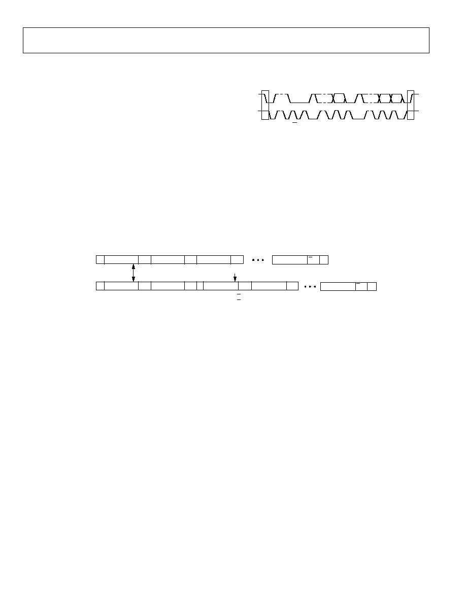
t
3
t
2
t
6
t
1
t
7
t
5
t
3
t
4
t
8
SDATA
SCLOCK
02980-0A
-002
Figure 2. MPU Port Timing Diagram
t
9
t
11
CLOCK
PIXEL INPUT
DATA
t
10
t
12
HSYNC,
FIELD/VSYNC,
BLANK
HSYNC,
FIELD/VSYNC,
BLANK
Cb
Y
Cr
Y
Cb
Y
t
14
CONTROL
I/PS
CONTROL
O/PS
S
t
13
02980-A
-
003
Figure 3. Pixel and Control Data Timing Diagram
t
16
t
17
t
18
TTXREQ
CLOCK
TTX
4 CLOCK
CYCLES
4 CLOCK
CYCLES
4 CLOCK
CYCLES
3 CLOCK
CYCLES
4 CLOCK
CYCLES
02980-A
-
004
Figure 4. Teletext Timing Diagram
ADV7174/ADV7179
Rev. A | Page 9 of 52
ABSOLUTE MAXIMUM RATINGS
Table 5.
Parameter
Rating
V
AA
to GND
4 V
Voltage on Any Digital Input Pin
GND 0.5 V to V
AA
+ 0.5 V
Storage Temperature (T
S
)
-65°C to +150°C
Junction Temperature (T
J
) 150°C
Lead Temperature
Soldering, 10 sec
260°C
Analog Outputs to GND
1
GND 0.5 V to V
AA
JA
2
30
°C/W
Stresses above those listed under Absolute Maximum Ratings
may cause permanent damage to the device. This is a stress
rating only; functional operation of the device at these or any
other conditions above those listed in the operational sections
of this specification is not implied. Exposure to absolute
maximum rating conditions for extended periods may affect
device reliability
__________________________________________________
1
Analog output short circuit to any power supply or common can be of an indefinite duration.
2
With the exposed metal paddle on the underside of LFCSP soldered to GND on the PCB.
ESD CAUTION
ESD (electrostatic discharge) sensitive device. Electrostatic charges as high as 4000 V readily accumulate on
the human body and test equipment and can discharge without detection. Although this product features
proprietary ESD protection circuitry, permanent damage may occur on devices subjected to high energy
electrostatic discharges. Therefore, proper ESD precautions are recommended to avoid performance
degradation or loss of functionality.
ADV7174/ADV7179
Rev. A | Page 10 of 52
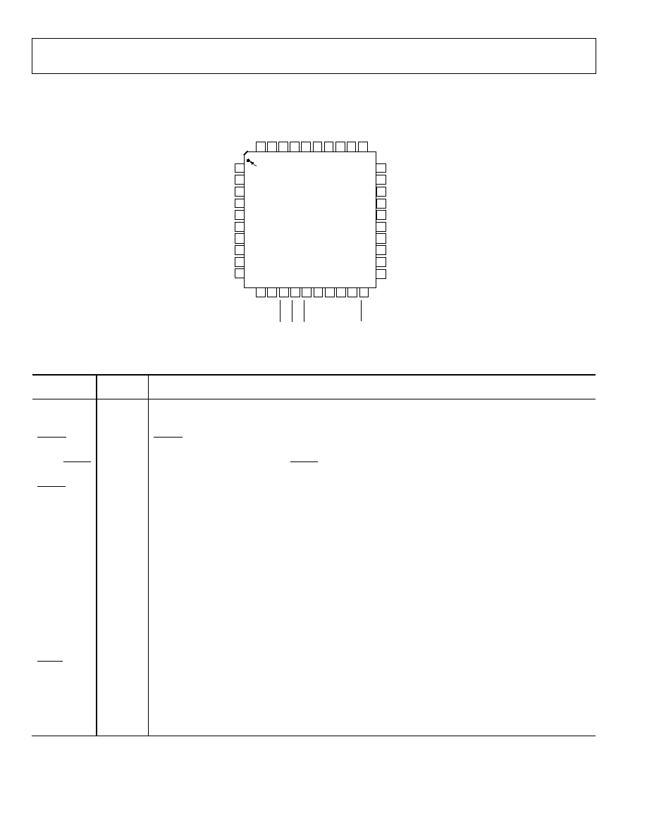
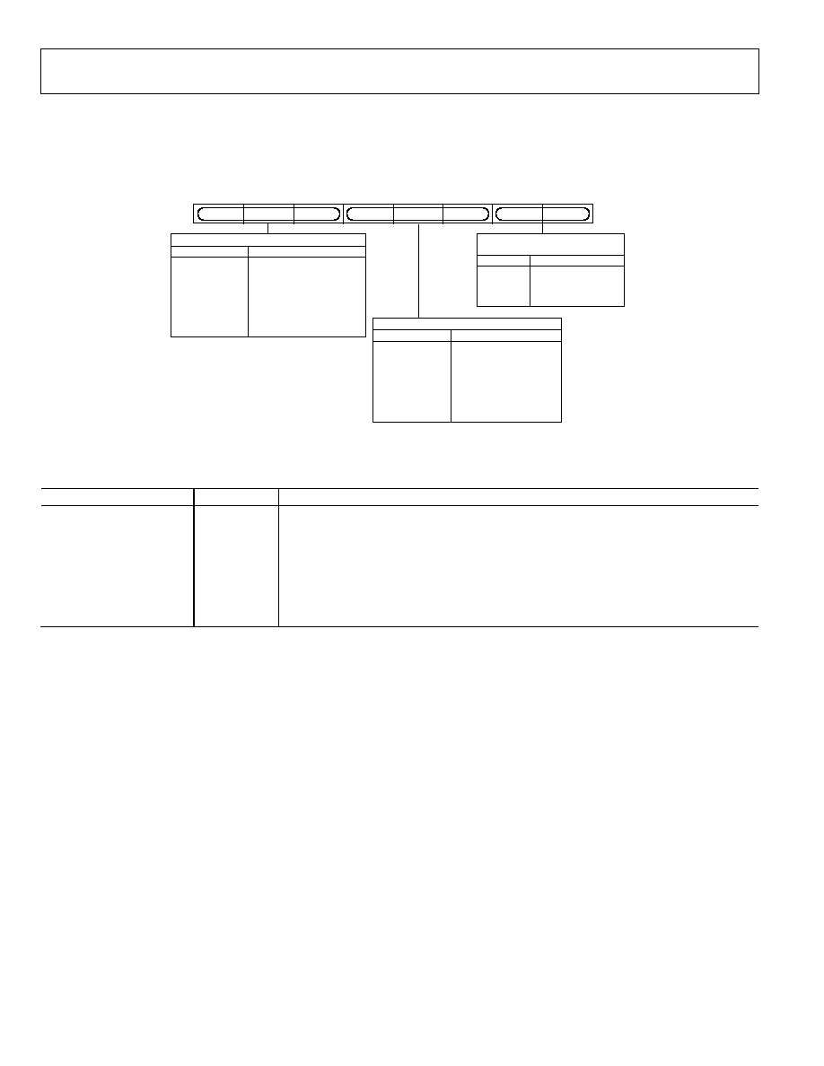
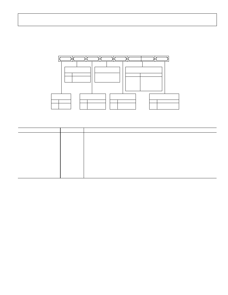
PIN CONFIGURATION AND FUNCTION DESCRIPTIONS
11 12 13 14 15 16 17 18 19 20
3
4
5
6
7
1
2
10
8
9
37 36 35
38
39
40
33 32
31
34
26
27
28
29
24
25
22
23
21
30
V
REF
DAC A
DAC B
V
AA
GND
V
AA
DAC C
BLANK
GND
GND
H
SYN
C
FIELD
/
VSYN
C
ALS
B
CLOCK
V
AA
P5
P6
P7
GND
GND
GND
GND
V
AA
COMP
SDATA
SCLOCK
GND
V
AA
GND
R
ESET
GND
P4
P3
P2
P1
P0
TTX
TTXREQ
R
SET
SC
R
ESET/
RTC
PIN 1
INDICATOR
ADV7174/ADV7179
LFCSP
TOP VIEW
(Not to Scale)
02980-A
-
005
Figure 5. Pin Configurations
Table 6. Pin Function Descriptions
Mnemonic
Input/
Output
Function
P7P0
I
8-Bit 4:2:2 Multiplexed YCrCb Pixel Port (P7P0). P0 is the LSB.
CLOCK
I
TTL Clock Input. Requires a stable 27 MHz reference clock for standard operation. Alternatively, a 24.5454 MHz
(NTSC) or 29.5 MHz (PAL) can be used for square pixel operation.
HSYNC
I/O
HSYNC (Modes 1 and 2) Control Signal. This pin may be configured to output (master mode) or accept (slave
mode) sync signals.
FIELD/VSYNC I/O
Dual Function FIELD (Mode 1) and VSYNC (Mode 2) Control Signal. This pin may be configured to output
(master mode) or accept (slave mode) these control signals.
BLANK
I/O
Video Blanking Control Signal. The pixel inputs are ignored when this is Logic 0. This signal is optional.
SCRESET/RTC I
This pin can be configured as an input by setting MR22 and MR21 of Mode Register 2. It can be configured as a
subcarrier reset pin, in which case a low-to-high transition on this pin resets the subcarrier to Field 0.
Alternatively, it can be configured as a real-time control (RTC) input.
V
REF
I/O
Voltage Reference Input for DACs or Voltage Reference Output (1.235 V).
R
SET
I
A 150 resistor connected from this pin to GND is used to control full-scale amplitudes of the video signals.
COMP
O
Compensation Pin. Connect a 0.1 µF capacitor from COMP to V
AA
. For optimum dynamic performance in low
power mode, the value of the COMP capacitor can be lowered to as low as 2.2 nF.
DAC A
O
DAC Output (see Table 13)
DAC B
O
DAC Output (see Table 13).
DAC C
O
DAC Output (see Table 13).
SCLOCK
I
MPU Port Serial Interface Clock Input.
SDATA
I/O
MPU Port Serial Data Input/Output.
ALSB
I
TTL Address Input. This signal sets up the LSB of the MPU address.
RESET
I
This input resets the on-chip timing generator and sets the ADV7174/ADV7179 into default mode. This is NTSC
operation, Timing Slave Mode 0, 8-bit operation, 2× composite out signals. DACs A, B, and C are enabled.
TTX
I
Teletext Data.
TTXREQ
O
Teletext Data Request Signal/Defaults to GND when Teletext Not Selected.
V
AA
P
Power Supply (2.8 V or 3.3 V).
GND
G
Ground Pin.

ADV7174/ADV7179
Rev. A | Page 11 of 52
GENERAL DESCRIPTION
The ADV7174/ADV7179 is an integrated digital video encoder
that converts digital CCIR-601 4:2:2 8-bit component video data
into a standard analog baseband television signal compatible
with worldwide standards.
The on-board SSAF (super sub-alias filter) with extended
luminance frequency response and sharp stop-band attenuation
enables studio quality video playback on modern TVs, giving
optimal horizontal line resolution.
An advanced power management circuit enables optimal con-
trol of power consumption in both normal operating modes
and in power-down or sleep modes.
The ADV7174/ADV7179 supports both PAL and NTSC square
pixel operation. The parts incorporate WSS and CGMS-A data
control generation.
The output video frames are synchronized with the incoming
data timing reference codes. Optionally, the encoder accepts
(and can generate) HSYNC, VSYNC, and FIELD timing signals.
These timing signals can be adjusted to change pulse width and
position while the part is in the master mode. The encoder
requires a signal two times the pixel rate (27 MHz) clock for
standard operation. Alternatively, the encoder requires a
24.5454 MHz clock for NTSC or 29.5 MHz clock for PAL
square pixel mode operation. All internal timing is generated
on-chip.
A separate Teletext port enables the user to directly input
Teletext data during the vertical blanking interval.
The ADV7174/ADV7179 modes are set up over a 2-wire serial
bidirectional port (I
2
C compatible) with two slave addresses.
The ADV7174/ADV7179 is packaged in a 40-lead 6 mm × 6 mm
LFCSP package.
DATA PATH DESCRIPTION
For PAL B/D/G/H/I/M/N and NTSC M and N modes, YCrCb
4:2:2 data is input via the CCIR-656 compatible pixel port at a
27 MHz data rate. The pixel data is demultiplexed to form three
data paths. Y typically has a range of 16 to 235, and Cr and Cb
typically have a range of 128 ± 112; however, it is possible to
input data from 1 to 254 on both Y, Cb, and Cr. The ADV7174/
ADV7179 supports PAL (B/D/G/H/I/M/N) and NTSC (with
and without pedestal) standards. The appropriate SYNC, BLANK,
and burst levels are added to the YCrCb data. Macrovision Anti-
taping (ADV7174 only), closed-captioning, and Teletext levels
are also added to Y and the resultant data is interpolated to a
rate of 27 MHz. The interpolated data is filtered and scaled by
three digital FIR filters.
The U and V signals are modulated by the appropriate subcarrier
sine/cosine phases and added together to make up the chromi-
nance signal. The luma (Y) signal can be delayed 13 luma
cycles (each cycle is 74 ns) with respect to the chroma signal.
The luma and chroma signals are then added together to make
up the composite video signal. All edges are slew rate limited.
The YCrCb data is also used to generate RGB data with
appropriate SYNC and BLANK levels. The RGB data is in
synchronization with the composite video output. Alternatively,
analog YPbPr data can be generated instead of RGB data.
The three l0-bit DACs can be used to output:
·
Composite Video + Composite Video
·
S-Video + Composite Video
·
YPrPb Video
·
SCART RGB Video
Alternatively, each DAC can be individually powered off if not
required.
Video output levels are illustrated in Appendix 6.
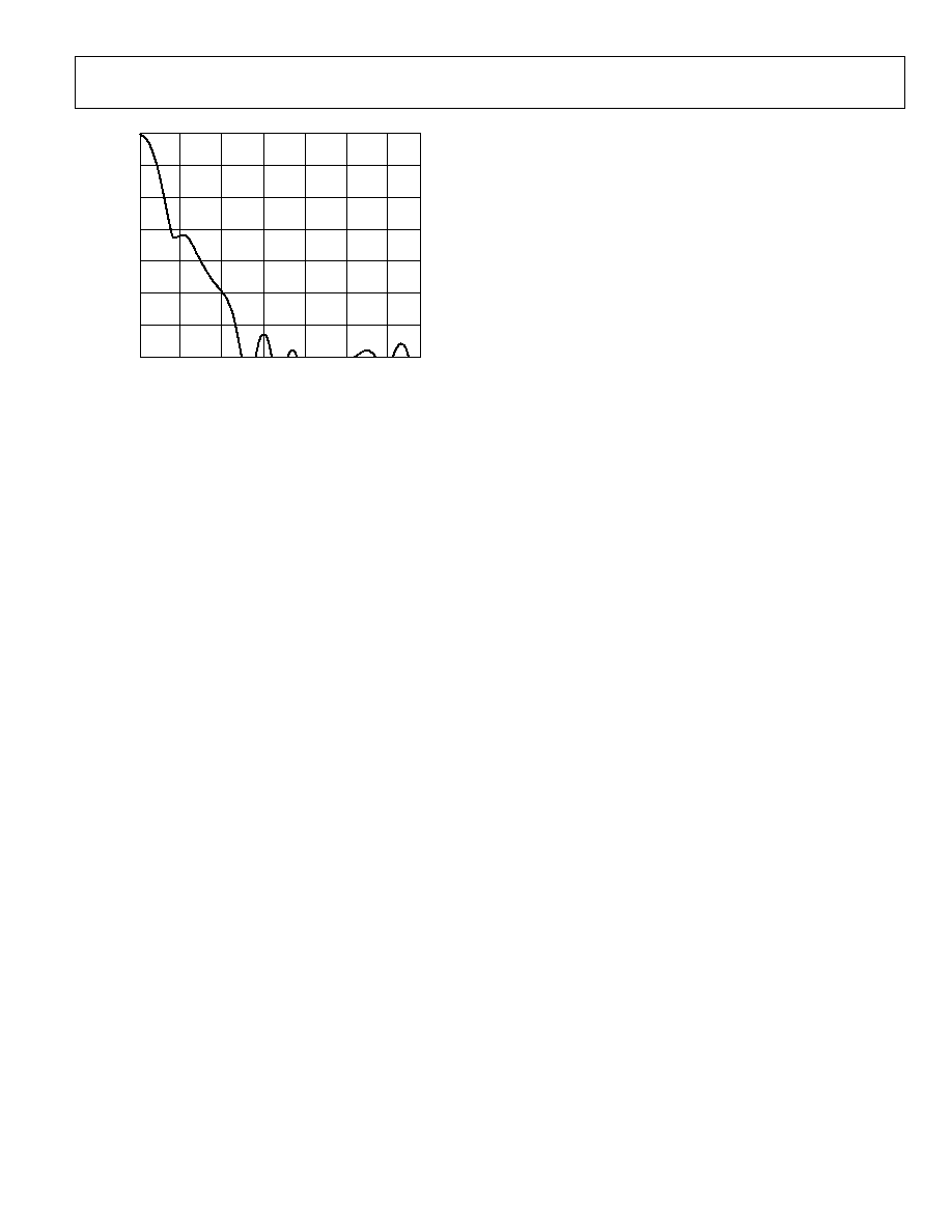
INTERNAL FILTER RESPONSE
The Y filter supports several different frequency responses,
including two low-pass responses, two notch responses, an
extended (SSAF) response, a CIF response, and a QCIF
response. The UV filter supports several different frequency
responses, including four low-pass responses, a CIF response,
and a QCIF response. These can be seen in Table 7 and Table 8
and Figure 6 to Figure 18.

ADV7174/ADV7179
Rev. A | Page 12 of 52
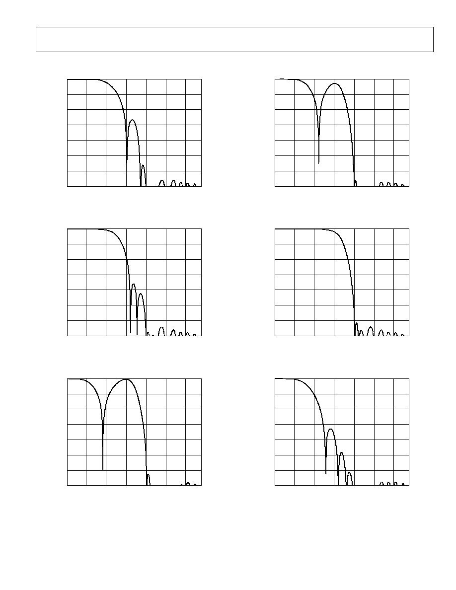
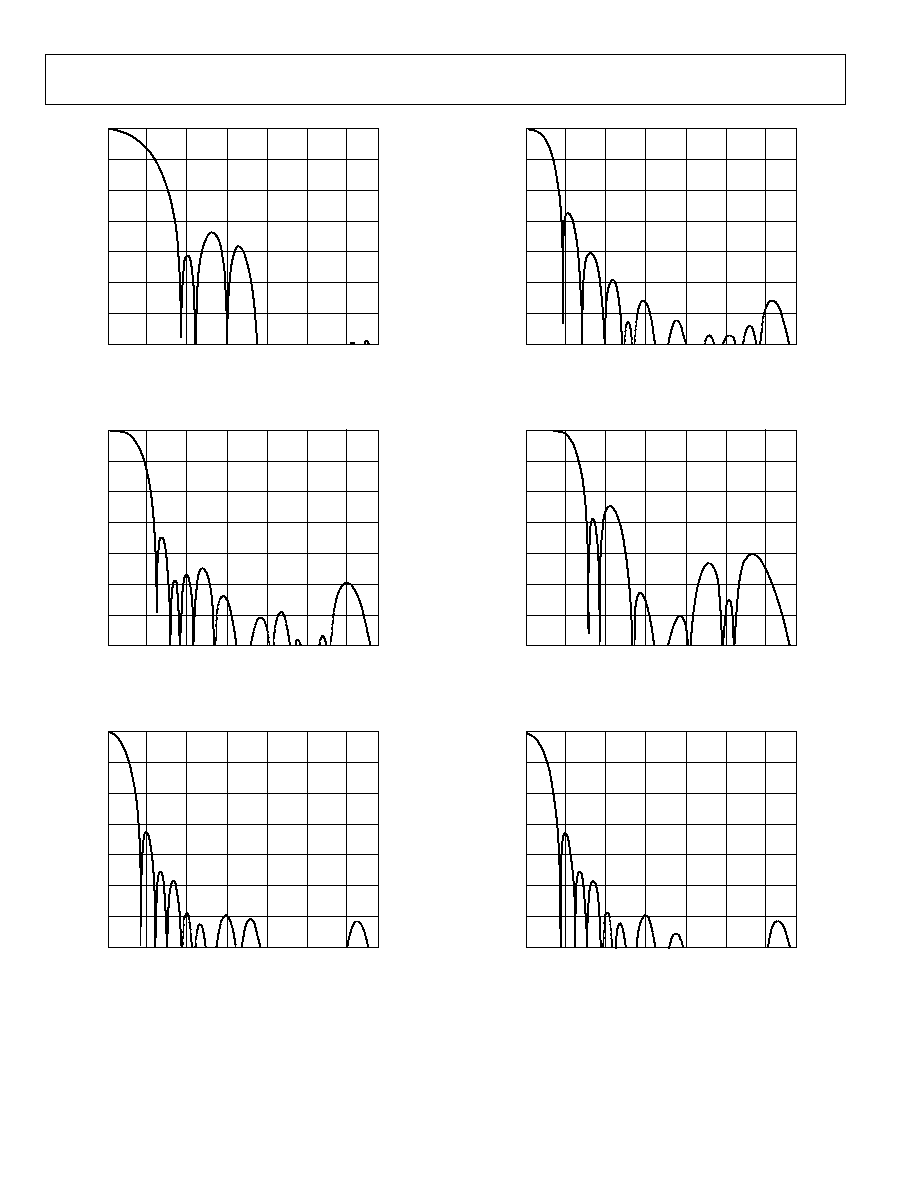
Table 7. Luminance Internal Filter Specifications
Filter Type
Filter Selection
Pass-Band Ripple
(dB)
3 dB Bandwidth
(MHz)
Stop-Band Cutoff
(MHz)
Stop-Band Attenuation
(dB)
MR04 MR03 MR02
Low-Pass
(NTSC)
0 0 0 0.091
4.157
7.37
-56
Low-Pass
(PAL)
0 0 1 0.15
4.74
7.96
-64
Notch
(NTSC)
0 1 0 0.015
6.54
8.3
-68
Notch
(PATL)
0 1 1 0.095
6.24
8.0
-66
Extended
(SSAF)
1 0 0 0.051
6.217
8.0
-61
CIF
1 0 1 0.018
3.0
7.06
-61
QCIF
1 1 0 Monotonic
1.5
7.15
-50
Table 8. Chrominance Internal Filter Specifications
Filter Type
Filter Selection
Pass-Band Ripple
(dB)
3 dB Bandwidth
(MHz)
Stop-Band Cutoff
(MHz)
Stop-Band Attenuation
(dB)
MR07 MR06 MR05
1.3 MHz
Low-Pass
0 0 0 0.084
1.395
3.01
-45
0.65 MHz
Low-Pass
0 0 1 Monotonic
0.65
3.64
-58.5
1.0 MHz
Low-Pass
0 1 0 Monotonic
1.0
3.73
-49
2.0 MHz
Low-Pass
0 1 1 0.0645
2.2
5.0
-40
Reserved 1 0 0
CIF
1 0 1 0.084
0.7
3.01
-45
QCIF
1 1 0 Monotonic
0.5
4.08
-50
ADV7174/ADV7179
Rev. A | Page 13 of 52
TYPICAL PERFORMANCE CHARACTERISTICS
FREQUENCY (MHz)
0
0
12
2
MAGNITUDE
(dB)
4
6
8
10
10
20
30
50
60
40
70
02980-A
-
006
Figure 6. Chrominance Internal Filter Specifications
FREQUENCY (MHz)
0
0
12
2
MAGNITUDE
(dB)
4
6
8
10
10
20
30
50
60
40
70
02980-A
-
007
Figure 7. PAL Low-Pass Luma Filter
FREQUENCY (MHz)
0
0
12
2
MAGNITUDE
(dB)
4
6
8
10
10
20
30
50
60
40
70
02980-A
-
008
Figure 8. NTSC Notch Luma Filter
FREQUENCY (MHz)
0
0
12
2
MAGNITUDE
(dB)
4
6
8
10
10
20
30
50
60
40
70
02980-A
-
009
Figure 9. PAL Notch Luma Filter
FREQUENCY (MHz)
0
0
12
2
MAGNITUDE
(dB)
4
6
8
10
10
20
30
50
60
40
70
02980-A
-
010
Figure 10. Extended Mode (SSAF) Luma Filter
FREQUENCY (MHz)
0
0
12
2
MAGNITUDE
(dB)
4
6
8
10
10
20
30
50
60
40
70
02980-A
-
011
Figure 11. CIF Luma Filter
ADV7174/ADV7179
Rev. A | Page 14 of 52
FREQUENCY (MHz)
0
0
12
2
MAGNITUDE
(dB)
4
6
8
10
10
20
30
50
60
40
70
02980-A
-
012
Figure 12. QCIF Luma Filter
FREQUENCY (MHz)
0
0
12
2
MAGNITUDE
(dB)
4
6
8
10
10
20
30
50
60
40
70
02980-A
-
013
Figure 13. 1.3 MHz Low-Pass Chroma Filter
FREQUENCY (MHz)
0
0
12
2
MAGNITUDE
(dB)
4
6
8
10
10
20
30
50
60
40
70
02980-A
-
014
Figure 14. 0.65 MHz Low-Pass Chroma Filter
FREQUENCY (MHz)
0
0
12
2
MAGNITUDE
(dB)
4
6
8
10
10
20
30
50
60
40
70
02980-A
-
015
Figure 15. 1.0 MHz Low-Pass Chroma Filter
FREQUENCY (MHz)
0
0
12
2
MAGNITUDE
(dB)
4
6
8
10
10
20
30
50
60
40
70
02980-A
-
016
Figure 16. 2.0 MHz Low-Pass Chroma Filter
FREQUENCY (MHz)
0
0
12
2
MAGNITUDE
(dB)
4
6
8
10
10
20
30
50
60
40
70
02980-A
-
017
Figure 17. CIF Chroma Filter
ADV7174/ADV7179
Rev. A | Page 15 of 52
FREQUENCY (MHz)
0
0
12
2
MAGNITUDE
(dB)
4
6
8
10
10
20
30
50
60
40
70
02980-A
-
018
Figure 18. QCIF Chroma Filter

ADV7174/ADV7179
Rev. A | Page 16 of 52
FEATURES
COLOR BAR GENERATION
The ADV7174/ADV7179 can be configured to generate 100/
7.5/75/7.5 color bars for NTSC or 100/0/75/0 for PAL color
bars. These are enabled by setting MR17 of Mode Register 1 to
Logic 1.
SQUARE PIXEL MODE
The ADV7174/ADV7179 can be used to operate in square pixel
mode. For NTSC operation, an input clock of 24.5454 MHz is
required. Alternatively, for PAL operation, an input clock of
29.5 MHz is required. The internal timing logic adjusts accord-
ingly for square pixel mode operation.
COLOR SIGNAL CONTROL
The color information can be switched on and off the video
output using Bit MR24 of Mode Register 2.
BURST SIGNAL CONTROL
The burst information can be switched on and off the video
output using Bit MR25 of Mode Register 2.
NTSC PEDESTAL CONTROL
The pedestal on both odd and even fields can be controlled on a
line-by-line basis using the NTSC pedestal control registers.
This allows the pedestals to be controlled during the vertical
blanking interval.
PIXEL TIMING DESCRIPTION
The ADV7174/ADV7179 operates in an 8-bit YCrCb mode.
8-Bit YCrCb Mode
This default mode accepts multiplexed YCrCb inputs through
the P7P0 pixel inputs. The inputs follow the sequence Cb0, Y0
Cr0, Y1, Cb1, Y2, and so on. The Y, Cb, and Cr data are input on
a rising clock edge.
SUBCARRIER RESET
Together with the SCRESET/RTC pin and Bits MR22 and
MR21 of Mode Register 2, the ADV7174/ADV7179 can be used
in subcarrier reset mode. The subcarrier resets to Field 0 at the
start of the following field when a low-to-high transition occurs
on this input pin.
REAL-TIME CONTROL
Together with the SCRESET/RTC pin and Bits MR22 and MR21
of Mode Register 2, the ADV7174/ADV7179 can be used to
lock to an external video source. The real-time control mode
allows the ADV7174/ADV7179 to automatically alter the
subcarrier frequency to compensate for line length variation.
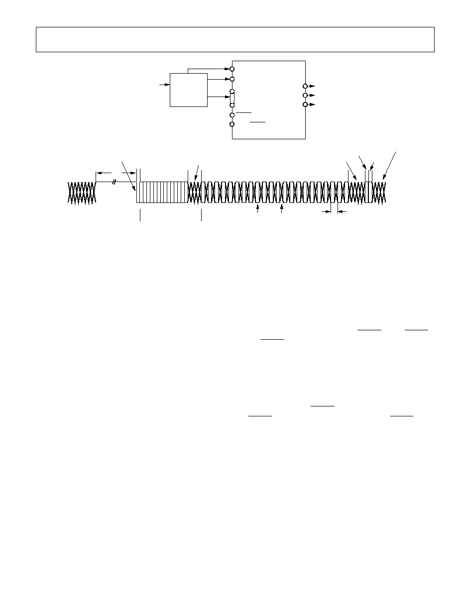
When the part is connected to a device that outputs a digital
data stream in the RTC format (such as a ADV7183A video
decoder; see Figure 19), the part automatically changes to the
compensated subcarrier frequency on a line-by-line basis. This
digital data stream is 67 bits wide and the subcarrier is contained
in Bits 0 to 21. Each bit is two clock cycles long. 00H should be
written into all four subcarrier frequency registers when using
this mode.
Video Timing Description
The ADV7174/ADV7179 is intended to interface with off-the-
shelf MPEG1 and MPEG2 decoders. Consequently, the
ADV7174/ADV7179 accepts 4:2:2 YCrCb pixel data via a
CCIR-656 pixel port and has several video timing modes of
operation that allow it to be configured as either a system
master video timing generator or as a slave to the system video
timing generator. The ADV7174/ADV7179 generates all of the
required horizontal and vertical timing periods and levels for
the analog video outputs.
The ADV7174/ADV7179 calculates the width and placement of
analog sync pulses, blanking levels, and color burst envelopes.
Color bursts are disabled on appropriate lines, and serration and
equalization pulses are inserted where required.
In addition, the ADV7174/ADV7179 supports a PAL or NTSC
square pixel operation in slave mode. The part requires an input
pixel clock of 24.5454 MHz for NTSC and an input pixel clock
of 29.5 MHz for PAL. The internal horizontal line counters
place the various video waveform sections into the correct
location for the new clock frequencies.
The ADV7174/ADV7179 has four distinct master and four
distinct slave timing configurations. Timing control is
established with the bidirectional HSYNC, BLANK, and
FIELD/VSYNC pins. Timing Mode Register 1 can also be used
to vary the timing pulse widths and where they occur in
relation to each other.
ADV7174/ADV7179
Rev. A | Page 17 of 52
COMPOSITE
VIDEO
(e.g., VCR
OR CABLE)
HSYNC
FIELD/VSYNC
CLOCK
GREEN/LUMA/Y
RED/CHROMA/Pr
BLUE/COMPOSITE/Pb
AD7174/ADV7179
P7P0
SCRESET/RTC
VIDEO
DECODER
(e.g., ADV7183A)
H/LTRANSITION
COUNT START
4 BITS
RESERVED
5 BITS
RESERVED
RESET
BIT
3
SEQUENCE
BIT
2
RESERVED
14 BITS
RESERVED
LOW
128
RTC
TIME SLOT: 01
14
67 68
NOT USED IN THE
ADV7174/ADV7179
19
VALID
SAMPLE
INVALID
SAMPLE
F
SC
PLL INCREMENT
1
8/LLC
21
0
13
NOTES
1
F
SC
PLL INCREMENT IS 22 BITS LONG, VALUE LOADED INTO ADV7174/ADV7179 F
SC
DDS REGISTER IS
F
SC
PLL INCREMENT BITS 21:0 PLUS BITS 0:9 OF THE SUBCARRIER FREQUENCY REGISTERS. ALL ZEROS SHOULD
BE WRITTEN TO THE SUBCARRIER FREQUENCY REGISTERS OF THE ADV7174/ADV7179.
2
SEQUENCE BIT
PAL: 0 = LINE NORMAL, 1 = LINE INVERTED
NTSC: 0 = NO CHANGE
3
RESET BIT
RESET ADV7174/ADV7179 DDS
0
02980-A
-
019
Figure 19. RTC Timing and Connections
Vertical Blanking Data Insertion
It is possible to allow encoding of incoming YCbCr data on
those lines of VBI that do not bear line sync or pre-/post-
equalization pulses (see Figure 21 to Figure 32). This mode of
operation is called partial blanking and is selected by setting
MR32 to 1. It allows the insertion of any VBI data (opened VBI)
into the encoded output waveform. This data is present in the
digitized incoming YCbCr data stream, for example. WSS data,
CGMS, VPS, and so on. Alternatively, the entire VBI may be
blanked (no VBI data inserted) on these lines by setting MR32
to 0.
Mode 0 (CCIR-656): Slave Option
(Timing Register 0 TR0 = X X X X X 0 0 0)
The ADV7174/ADV7179 is controlled by the SAV (start active
video) and EAV (end active video) time codes in the pixel data.
All timing information is transmitted using a 4-byte synchro-
nization pattern. A synchronization pattern is sent immediately
before and after each line during active picture and retrace.
Mode 0 is illustrated in Figure 20. The HSYNC, FIELD/VSYNC,
and BLANK (if not used) pins should be tied high during this
mode.
Mode 0 (CCIR-656): Master Option
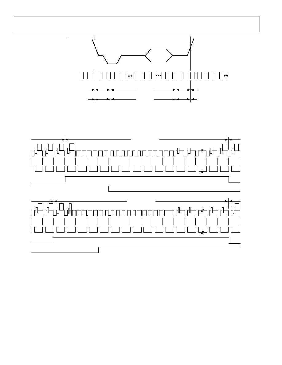
(Timing Register 0 TR0 = X X X X X 0 0 1)
The ADV7174/ADV7179 generates H, V, and F signals required
for the SAV and EAV time codes in the CCIR-656 standard. The
H bit is output on the HSYNC pin, the V bit is output on the
BLANK pin, and the F bit is output on the FIELD/VSYNC pin.
Mode 0 is illustrated in Figure 21 (NTSC) and Figure 22 (PAL).
The H, V, and F transitions relative to the video waveform are
illustrated in Figure 23.
ADV7174/ADV7179
Rev. A | Page 18 of 52
Y
C
r
Y F
F
0
0
0
0
X
Y
8
0
1
0
8
0
1
0
F
F
0
0
F
F
A
B
A
B
A
B
8
0
1
0
8
0
1
0
F
F
0
0
0
0
X
Y
C
b
Y C
r
C
b
Y
C
b
Y
C
r
EAV CODE
SAV CODE
ANCILLARY DATA
(HANC)
4 CLOCK
4 CLOCK
268 CLOCK
1440 CLOCK
4 CLOCK
4 CLOCK
280 CLOCK
1440 CLOCK
END OF ACTIVE
VIDEO LINE
START OF ACTIVE
VIDEO LINE
ANALOG
VIDEO
INPUT PIXELS
NTSC/PAL M SYSTEM
(525 LlNES/60Hz)
PAL SYSTEM
(625 LINES/50Hz)
Y
02980-A
-
020
Figure 20. Timing Mode 0 (Slave Mode)
522
523
524
525
1
2
3
4
5
6
7
8
9
10
11
20
21
22
DISPLAY
DISPLAY
VERTICAL BLANK
ODD FIELD
EVEN FIELD
H
V
F
260
261
262
263
264
265
266
267
268
269
270
271
272
273
274
283
284
285
ODD FIELD
EVEN FIELD
DISPLAY
DISPLAY
VERTICAL BLANK
H
V
F
02980-A
-
021
Figure 21. Timing Mode 0 (NTSC Master Mode)
ADV7174/ADV7179
Rev. A | Page 19 of 52
622
623
624
625
1
2
3
4
5
6
7
21
22
23
DISPLAY
DISPLAY
VERTICAL BLANK
H
V
F
ODD FIELD
EVEN FIELD
309
310
311
312
314
315
316
317
318
319
320
334
335
336
DISPLAY
DISPLAY
VERTICAL BLANK
H
V
F
ODD FIELD
EVEN FIELD
313
02980-A
-
022
Figure 22. Timing Mode 0 (PAL Master Mode)
ANALOG
VIDEO
H
F
V
02980-A
-
023
Figure 23. Timing Mode 0 Data Transitions (Master Mode)
ADV7174/ADV7179
Rev. A | Page 20 of 52
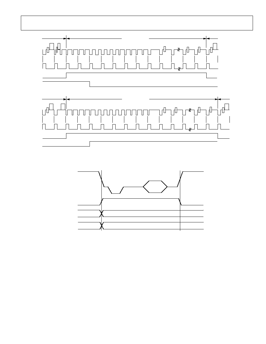
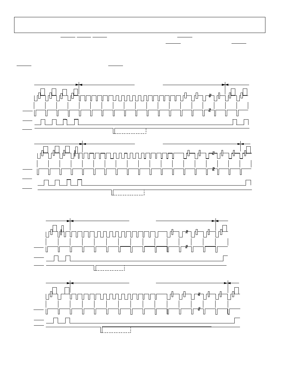
Mode 1: Slave Option HSYNC, BLANK, FIELD
(Timing Register 0 TR0 = X X X X X 0 1 0)
In this mode, the ADV7174/ADV7179 accepts horizontal SYNC
and odd/even FIELD signals. A transition of the FIELD input
when HSYNC is low indicates a new frame, i.e., vertical retrace.
The BLANK signal is optional. When the BLANK input is
disabled, the ADV7174/ADV7179 automatically blanks all
normally blank lines as per CCIR-624. Mode 1 is illustrated in
Figure 24 (NTSC) and Figure 25 (PAL).
260
261
262
263
264
265
266
267
268
269
270
271
272
273
274
283
284
285
ODD FIELD
EVEN FIELD
DISPLAY
DISPLAY
HSYNC
BLANK
FIELD
522
523
524
525
1
2
3
4
5
6
7
8
9
10
11
20
21
22
DISPLAY
DISPLAY
ODD FIELD
EVEN FIELD
HSYNC
BLANK
FIELD
VERTICAL BLANK
VERTICAL BLANK
02980-A
-
024
Figure 24. Timing Mode 1 (NTSC)
622
623
624
625
1
2
3
4
5
6
7
21
22
23
DISPLAY
ODD FIELD
EVEN FIELD
HSYNC
BLANK
FIELD
DISPLAY
309
310
311
312
313
314
315
316
317
318
319
334
335
336
DISPLAY
ODD FIELD
EVEN FIELD
HSYNC
BLANK
FIELD
DISPLAY
320
VERTICAL BLANK
VERTICAL BLANK
02980-A
-
025
Figure 25. Timing Mode 1 (PAL)
ADV7174/ADV7179
Rev. A | Page 21 of 52
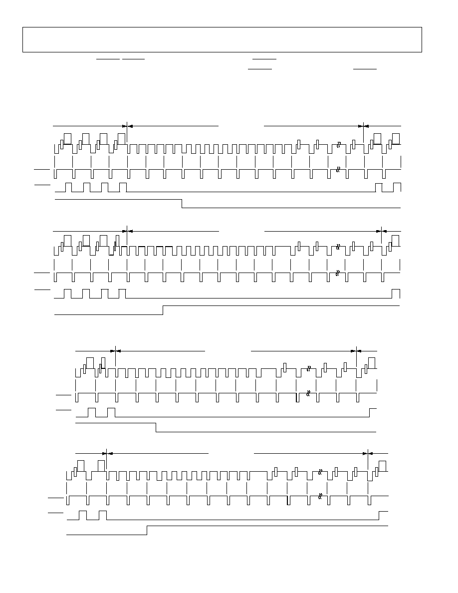
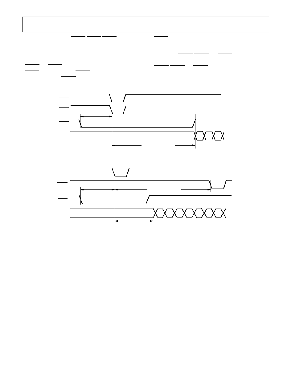
Mode 1: Master Option HSYNC, BLANK, FIELD
(Timing Register 0 TR0 = X X X X X 0 1 1)
In this mode, the ADV7174/ADV7179 can generate horizontal
SYNC and odd/even FIELD signals. A transition of the FIELD
input when HSYNC is low indicates a new frame, i.e., vertical
retrace. The BLANK signal is optional. When the BLANK input
is disabled, the ADV7174/ADV7179 automatically blanks all
normally blank lines as per CCIR-624. Pixel data is latched on
the rising clock edge following the timing signal transitions.
Mode 1 is illustrated in Figure 24 (NTSC) and Figure 25 (PAL).
Figure 26 illustrates the HSYNC, BLANK, and FIELD for an
odd or even field transition relative to the pixel data.
FIELD
PIXEL
DATA
PAL = 12
×
CLOCK/2
NTSC = 16
×
CLOCK/2
PAL = 132
×
CLOCK/2
NTSC = 122
×
CLOCK/2
Cb
Y
Cr
Y
HSYNC
BLANK
02980-A
-
026
Figure 26. Timing Mode 1 Odd/Even Field Transitions Master/Slave
ADV7174/ADV7179
Rev. A | Page 22 of 52
Mode 2: Slave Option HSYNC, VSYNC, BLANK
(Timing Register 0 TR0 = X X X X X 1 0 0)
In this mode, the ADV7174/ADV7179 accepts horizontal and
vertical SYNC signals. A coincident low transition of both and
VSYNC inputs indicates the start of an odd field. A VSYNC low
transition when HSYNC is high indicates the start of an even
field. The BLANK signal is optional. When the BLANK input is
disabled, the ADV7174/ADV7179 automatically blanks all
normally blank lines as per CCIR-624. Mode 2 is illustrated in
Figure 27 (NTSC) and Figure 28 (PAL).
522
523
524
525
1
2
3
4
5
6
7
8
9
10
11
20
21
22
DISPLAY
DISPLAY
ODD FIELD
EVEN FIELD
HSYNC
BLANK
VSYNC
260
261
262
263
264
265
266
267
268
269
270
271
272
273
274
283
284
285
ODD FIELD
EVEN FIELD
DISPLAY
DISPLAY
HSYNC
BLANK
VSYNC
VERTICAL BLANK
VERTICAL BLANK
02980-A
-
027
Figure 27. Timing Mode 2 (NTSC)
622
623
624
625
1
2
3
4
5
6
7
21
22
23
DISPLAY
ODD FIELD
EVEN FIELD
HSYNC
BLANK
VSYNC
DISPLAY
309
310
311
312
313
314
315
316
317
318
319
334
335
336
DISPLAY
ODD FIELD
EVEN FIELD
HSYNC
BLANK
DISPLAY
320
VSYNC
VERTICAL BLANK
VERTICAL BLANK
02980-A
-
028
Figure 28. Timing Mode 2 (PAL)
ADV7174/ADV7179
Rev. A | Page 23 of 52
Mode 2: Master Option HSYNC, VSYNC, BLANK
(Timing Register 0 TR0 = X X X X X 1 0 1)
In this mode, the ADV7174/ADV7179 can generate horizontal
and vertical SYNC signals. A coincident low transition of both
HSYNC and VSYNC inputs indicates the start of an odd field. A
VSYNC low transition when HSYNC is high indicates the start
of an even field. The BLANK signal is optional. When the
BLANK input is disabled, the ADV7174/ADV7179 automatically
blanks all normally blank lines as per CCIR-624. Mode 2 is
illustrated in Figure 27 (NTSC) and Figure 28 (PAL). Figure 29
illustrates the HSYNC, BLANK, and VSYNC for an even-to-odd
field transition relative to the pixel data. Figure 30 illustrates the
HSYNC, BLANK, and VSYNC for an odd-to-even field
transition relative to the pixel data.
HSYNC
VSYNC
BLANK
PIXEL
DATA
Cb
Y
Cr
Y
PAL = 12
×
CLOCK/2
NTSC = 16
×
CLOCK/2
PAL = 132
×
CLOCK/2
NTSC = 122
×
CLOCK/2
02980-A
-
029
Figure 29. Timing Mode 2 Even-to-Odd Field Transition Master/Slave
VSYNC
PIXEL
DATA
Cb
Y
Cr
Y
Cb
HSYNC
BLANK
PAL = 12
×
CLOCK/2
NTSC = 16
×
CLOCK/2
PAL = 132
×
CLOCK/2
NTSC = 122
×
CLOCK/2
PAL = 864
×
CLOCK/2
NTSC = 858
×
CLOCK/2
02980-A
-
082
Figure 30. Timing Mode 2 Odd-to-Even Field Transition Master/Slave
ADV7174/ADV7179
Rev. A | Page 24 of 52
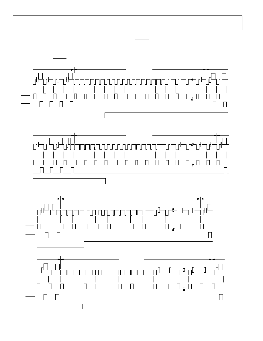
Mode 3: Master/Slave Option HSYNC, BLANK, FIELD
(Timing Register 0 TR0 = X X X X X 1 1 0 or X X X X X 1 1 1)
In this mode, the ADV7174/ADV7179 accepts or generates
horizontal SYNC and odd/even FIELD signals. A transition of
the FIELD input when HSYNC is high indicates a new frame,
that is, vertical retrace. The BLANK signal is optional. When the
BLANK input is disabled, the ADV7174/ADV7179 automatically
blanks all normally blank lines as per CCIR-624. Mode 3 is
illustrated in Figure 31 (NTSC) and Figure 32 (PAL).
522
523
524
525
1
2
3
4
5
6
7
8
9
10
11
20
21
22
DISPLAY
DISPLAY
VERTICAL BLANK
ODD FIELD
EVEN FIELD
BLANK
FIELD
260
261
262
263
264
265
266
267
268
269
270
271
272
273
274
283
284
285
DISPLAY
DISPLAY
VERTICAL BLANK
HSYNC
ODD FIELD
BLANK
FIELD
HSYNC
EVEN FIELD
02980-A
-
030
Figure 31. Timing Mode 3 (NTSC)
622
623
624
625
1
2
3
4
5
6
7
21
22
23
DISPLAY
DISPLAY
VERTICAL BLANK
ODD FIELD
EVEN FIELD
BLANK
FIELD
309
310
311
312
314
315
316
317
318
319
320
334
335
336
DISPLAY
DISPLAY
VERTICAL BLANK
ODD FIELD
EVEN FIELD
313
HSYNC
BLANK
FIELD
HSYNC
02980-A
-
031
Figure 32. Timing Mode 3 (PAL)
ADV7174/ADV7179
Rev. A | Page 25 of 52
POWER-ON RESET
After power-up, it is necessary to execute a reset operation. A
reset occurs on the falling edge of a high-to-low transition on
the RESET pin. This initializes the pixel port so that the pixel
inputs, P7P0, are selected. After reset, the ADV7174/ADV7179
is automatically set up to operate in NTSC mode. Subcarrier
frequency code 21F07C16H is loaded into the subcarrier
frequency registers. All other registers, with the exception of
Mode Register 0, are set to 00H. With the exception of Bit MR44,
all bits in Mode Register 0 are set to Logic 0. Bit MR44 of Mode
Register 4 is set to Logic 1. This enables the 7.5 IRE pedestal.
SCH PHASE MODE
The SCH phase is configured in default mode to reset every
four (NTSC) or eight (PAL) fields to avoid an accumulation of
SCH phase error over time. In an ideal system, 0 SCH phase
error would be maintained forever, but in reality, this is impossi-
ble to achieve due to clock frequency variations. This effect is
reduced by the use of a 32-bit DDS, which generates this SCH.
Resetting the SCH phase every four or eight fields avoids the
accumulation of SCH phase error and results in very minor
SCH phase jumps at the start of the 4- or 8-field sequence.
Resetting the SCH phase should not be done if the video source
does not have stable timing or the ADV7174/ADV7179 is
configured in RTC mode (MR21 = 1 and MR22 = 1). Under
these conditions (unstable video), the subcarrier phase reset
should be enabled (MR22 = 0 and MR21 = 1), but no reset
applied. In this configuration, the SCH phase can never be reset,
which means that the output video can now track the unstable
input video. The subcarrier phase reset, when applied, resets the
SCH phase to Field 0 at the start of the next field, for example,
subcarrier phase reset applied in Field 5 (PAL) on the start of
the next field SCH phase is reset to Field 0.
MPU PORT DESCRIPTION
The ADV7174/ADV7179 supports a 2-wire serial (I
2
C
compatible) microprocessor bus driving multiple peripherals.
Two inputs, serial data (SDATA) and serial clock (SCLOCK),
carry information between any device connected to the bus.
Each slave device is recognized by a unique address. The
ADV7174/ADV7179 has four possible slave addresses for both
read and write operations. These are unique addresses for each
device and are illustrated in Figure 33 and Figure 34. The LSB
sets either a read or write operation. Logic 1 corresponds to a
read operation, while Logic 0 corresponds to a write operation.
A 1 is set by setting the ALSB pin of the ADV7174/ ADV7179 to
Logic 0 or Logic 1.
1
X
1
0
1
0
1
A1
ADDRESS
CONTROL
SET UP BY
ALSB
READ/WRITE
CONTROL
0
WRITE
1
READ
02980-
A-
032
Figure 33. ADV7174 Slave Address
0
X
1
0
1
0
1
A1
ADDRESS
CONTROL
SET UP BY
ALSB
READ/WRITE
CONTROL
0
WRITE
1
READ
02980-
A-
033
Figure 34. ADV7179 Slave Address
To control the various devices on the bus, the following protocol
must be followed: first, the master initiates a data transfer by
establishing a start condition, defined by a high-to-low transition
on SDATA while SCLOCK remains high. This indicates that an
address/data stream will follow. All peripherals respond to the
start condition and shift the next eight bits (7-bit address + R/W
bit). The bits transfer from MSB down to LSB. The peripheral
that recognizes the transmitted address responds by pulling the
data line low during the ninth clock pulse. This is known as an
Acknowledge bit. All other devices withdraw from the bus at
this point and maintain an idle condition. The idle condition is
where the device monitors the SDATA and SCLOCK lines wait-
ing for the start condition and the correct transmitted address.
The R/W bit determines the direction of the data. A Logic 0 on
the LSB of the first byte means that the master will write infor-
mation to the peripheral. A Logic 1 on the LSB of the first byte
means that the master will read information from the peripheral.
The ADV7174/ADV7179 acts as a standard slave device on the
bus. The data on the SDATA pin is eight bits long, supporting
the 7-bit addresses plus the R/W bit. The ADV7174/ADV7179
has 26 subaddresses to enable access to the internal registers. It
therefore interprets the first byte as the device address and the
second byte as the starting subaddress. The subaddresses' auto
increment allows data to be written to or read from the starting
subaddress. A data transfer is always terminated by a stop
condition. The user can also access any unique subaddress
register on a one-by-one basis without having to update all the
registers. There is one exception. The subcarrier frequency
registers should be updated in sequence, starting with
Subcarrier Frequency Register 0. The auto increment function
should then be used to increment and access Subcarrier
Frequency Registers 1, 2, and 3. The subcarrier frequency
registers should not be accessed independently.
ADV7174/ADV7179
Rev. A | Page 26 of 52
Stop and start conditions can be detected at any stage during the
data transfer. If these conditions are asserted out of sequence with
normal read and write operations, they cause an immediate
jump to the idle condition. During a given SCLOCK high period,
the user should issue only one start condition, one stop condition,
or a single stop condition followed by a single start condition. If
an invalid subaddress is issued by the user, the ADV7174/
ADV7179 cannot issue an acknowledge and returns to the idle
condition. If in auto-increment mode the user exceeds the
highest subaddress, the following action is taken:
1.
In read mode, the highest subaddress register contents
continues to be output until the master device issues a no-
acknowledge. This indicates the end of a read. A no-
acknowledge condition is when the SDATA line is not
pulled low on the ninth pulse.
2.
In write mode, the data for the invalid byte is not loaded
into any subaddress register, a no-acknowledge is issued by
the ADV7174/ADV7179, and the part returns to the idle
condition.
Figure 35 illustrates an example of data transfer for a read
sequence and the start and stop conditions.
Figure 36 shows bus write and read sequences.
17
8
9
17
8
9
17
8
9
P
S
START ADDR R/W ACK SUBADDRESS ACK
DATA
ACK
STOP
SDATA
SCLOCK
02980-A-034
Figure 35. Bus Data Transfer
REGISTER ACCESSES
The MPU can write to or read from all of the ADV7174/
ADV7179 registers except the subaddress register, which is a
write-only register. The subaddress register determines which
register the next read or write operation accesses. All commu-
nications with the part through the bus start with an access to
the subaddress register. A read/write operation is performed
from to the target address, which then increments to the next
address until a stop command on the bus is performed.
DATA
A(S)
S SLAVE ADDR A(S)
SUB ADDR
A(S)
LSB = 0
LSB = 1
DATA
P
S SLAVE ADDR A(S)
SUB ADDR A(S) S SLAVE ADDR A(S)
DATA
A(M)
DATA
P
WRITE
SEQUENCE
READ
SEQUENCE
A(S) = NO-ACKNOWLEDGE BY SLAVE
A(M) = NO-ACKNOWLEDGE BY MASTER
A(S) = ACKNOWLEDGE BY SLAVE
A(M) = ACKNOWLEDGE BY MASTER
S = START BIT
P = STOP BIT
A(S)
A(M)
02980-A
-
035
Figure 36. Write and Read Sequences

ADV7174/ADV7179
Rev. A | Page 27 of 52
REGISTER PROGRAMMING
This section describes the configuration of each register,
including the subaddress register, mode registers, subcarrier
frequency registers, the subcarrier phase register, timing
registers, closed captioning extended data registers, closed
captioning data registers, and NTSC pedestal control registers.
SUBADDRESS REGISTER (SR7SR0)
The communications register is an 8-bit write-only register.
After the part has been accessed over the bus and a read/write
operation is selected, the subaddress is set up. The subaddress
register determines to/from which register the operation takes
place.
Figure 37 shows the various operations under the control of the
subaddress register. Zero should always be written to SR7SR6.
REGISTER SELECT (SR5SR0)
These bits are set up to point to the required starting address.
SR4
SR3
SR2
SR1
SR0
SR7
SR6
SR5
ZERO SHOULD BE WRITTEN
TO THESE BITS
SR7 SR6(000)
POWER-UP
VALUES
SR5 SR4 SR3 SR2 SR1 SR0
0
0
0
MODE REGISTER 0
0
0
1
MODE REGISTER 1
0
0
1
MODE REGISTER 2
0
0
1
MODE REGISTER 3
0
0
0
MODE REGISTER 4
0
0
0
RESERVED
0
0
1
RESERVED
0
0
1
TIMING MODE REGISTER 0
0
1
0
TIMING MODE REGISTER 1
0
1
0
SUBCARRIER FREQUENCY REGISTER 0
0
1
1
SUBCARRIER FREQUENCY REGISTER 1
0
1
1
SUBCARRIER FREQUENCY REGISTER 2
0
1
0
SUBCARRIER FREQUENCY REGISTER 3
0
1
0
SUBCARRIER PHASE REGISTER
0
1
1
CLOSED CAPTIONING EXTENDED DATA BYTE 0
0
1
1
CLOSED CAPTIONING EXTENDED DATA BYTE 1
0
0
0
CLOSED CAPTIONING DATA BYTE 0
0
0
0
CLOSED CAPTIONING DATA BYTE 1
0
0
1
NTSC PEDESTAL CONTROL REGISTER 0/
PAL TTX CONTROL REGISTER 0
0
0
1
NTSC PEDESTAL CONTROL REGISTER 1/
PAL TTX CONTROL REGISTER 1
0
0
0
NTSC PEDESTAL CONTROL REGISTER 2/
PAL TTX CONTROL REGISTER 2
0
0
0
NTSC PEDESTAL CONTROL REGISTER 3/
PAL TTX CONTROL REGISTER 3
0
0
1
CGMS_WSS_0
0
0
1
CGMS_WSS_1
0
1
0
CGMS_WSS_2
0
0
0
0
0
0
0
0
0
0
0
0
0
0
0
0
0
1
1
1
1
1
1
1
1
1
1
1
0
0
0
0
1
1
1
1
0
0
0
0
1
1
1
1
0
0
0
0
1
1
1
1
0
0
0
0
1
0
1
0
1
0
1
0
1
0
1
0
1
0
1
0
1
0
1
0
1
0
1
0
1
TELETEXT REQUEST CONTROL REGISTER
ADV7179 SUBADDRESS REGISTER
SR5 SR4 SR3 SR2 SR1 SR0
ADV7174 SUBADDRESS REGISTER
0
0
0
MODE REGISTER 0
0
0
0
MODE REGISTER 1
0
0
1
MODE REGISTER 2
0
0
1
MODE REGISTER 3
0
0
0
MODE REGISTER 4
0
0
0
RESERVED
0
0
1
RESERVED
0
0
1
TIMING MODE REGISTER 0
0
1
0
TIMING MODE REGISTER 1
0
1
0
SUBCARRIER FREQUENCY REGISTER 0
0
1
1
SUBCARRIER FREQUENCY REGISTER 1
0
1
1
SUBCARRIER FREQUENCY REGISTER 2
0
1
0
SUBCARRIER FREQUENCY REGISTER 3
0
1
0
SUBCARRIER PHASE REGISTER
0
1
1
CLOSED CAPTIONING EXTENDED DATA BYTE 0
0
1
1
CLOSED CAPTIONING EXTENDED DATA BYTE 1
0
0
0
CLOSED CAPTIONING DATA BYTE 0
0
0
0
CLOSED CAPTIONING DATA BYTE 1
0
0
1
NTSC PEDESTAL CONTROL REGISTER 0/
PAL TTX CONTROL REGISTER 0
0
0
1
NTSC PEDESTAL CONTROL REGISTER 1/
PAL TTX CONTROL REGISTER 1
0
0
0
NTSC PEDESTAL CONTROL REGISTER 2/
PAL TTX CONTROL REGISTER 2
0
0
0
NTSC PEDESTAL CONTROL REGISTER 3/
PAL TTX CONTROL REGISTER 3
0
0
1
CGMS_WSS_0
0
0
1
CGMS_WSS_1
0
1
0
CGMS_WSS_2
0
1
0
TELETEXT REQUEST CONTROL REGISTER
0
1
1
RESERVED
0
1
1
RESERVED
0
1
0
RESERVED
0
1
0
RESERVED
0
1
1
MACROVISION REGISTERS
0
1
1
MACROVISION REGISTERS
1
0
0
MACROVISION REGISTERS
1
0
0
MACROVISION REGISTERS
1
0
1
MACROVISION REGISTERS
1
0
1
MACROVISION REGISTERS
1
0
0
MACROVISION REGISTERS
1
0
0
MACROVISION REGISTERS
1
0
1
MACROVISION REGISTERS
1
0
1
MACROVISION REGISTERS
1
1
0
MACROVISION REGISTERS
1
1
0
MACROVISION REGISTERS
1
1
1
MACROVISION REGISTERS
1
1
1
MACROVISION REGISTERS
1
1
0
MACROVISION REGISTERS
1
1
0
MACROVISION REGISTERS
1
1
1
MACROVISION REGISTERS
1
0
0
0
0
0
0
0
0
0
0
0
0
0
0
0
0
1
1
1
1
1
1
1
1
1
1
1
1
1
1
1
1
0
0
0
0
0
0
0
0
0
0
0
0
0
0
0
0
1
0
0
0
0
1
1
1
1
0
0
0
0
1
1
1
1
0
0
0
0
1
1
1
1
0
0
0
0
1
1
1
1
0
0
0
0
1
1
1
1
0
0
0
0
1
1
1
1
1
0
1
0
1
0
1
0
1
0
1
0
1
0
1
0
1
0
1
0
1
0
1
0
1
0
1
0
1
0
1
0
1
0
1
0
1
0
1
0
1
0
1
0
1
0
1
0
1
00h
58h
00h
00h
10h
00h
00h
00h
00h
16h
7Ch
F0h
21h
00h
00h
00h
00h
00h
00h
00h
00h
00h
00h
00h
00h
00h
00h
00h
00h
00h
00h
00h
00h
00h
00h
00h
00h
00h
00h
00h
00h
00h
00h
00h
00h
00h
00h
00h
MACROVISION REGISTERS
02980-
A-
036
Figure 37. Subaddress Register Map
ADV7174/ADV7179
Rev. A | Page 28 of 52
MODE REGISTER 0 (MR0)
Bits:
MR07 MR00
Address:
SR4SR0 = 00H
Figure 38 shows the various operations under the control of Mode Register 0. This register can be read from as well as written to.
CHROMA FILTER SELECT
MR07 MR06
0 0 0 1.3 MHz LOW-PASS FILTER
MR05
0 0 1 0.65 MHz LOW-PASS FILTER
0 1 0 1.0 MHz LOW-PASS FILTER
0 1 1 2.0 MHz LOW-PASS FILTER
1 0 0 RESERVED
1 0 1 CIF
1 1 0 QCIF
1 1 1 RESERVED
MR01
MR00
MR07
MR02
MR03
MR05
MR06
MR04
OUTPUT VIDEO
STANDARD SELECTION
MR01 MR00
0 0 NTSC
0 1 PAL (B, D, G, H, and I)
1 0 PAL (M)
1 1 RESERVED
LUMA FILTER SELECT
MR04 MR03
0 0 0 LOW-PASS FILTER (NTSC)
MR02
0 0 1 LOW-PASS FILTER (PAL)
0 1 0 NOTCH FILTER (NTSC)
0 0 1 NOTCH FILTER (PAL)
1 0 0 EXTENDED MODE
1 0 1 CIF
1 1 0 QCIF
1 1 1 RESERVED
02980-A
-
037
Figure 38. Mode Register 0
Table 9. MR0 Bit Description
Bit Name
Bit No.
Description
Output Video Standard
Selection
MR01MR00
These bits are used to set up the ENCODE mode. The ADV7174/ADV7179 can be set up to
output NTSC, PAL (B/D/G/H/I), and PAL (M and N) standard video.
PAL M is available on the ADV7174 only.
Luminance Filter Control
MR02MR04
These bits specify which luminance filter is to be selected. The filter selection is made
independent of whether PAL or NTSC is selected.
Chrominance Filter Control MR05MR07
These bits select the chrominance filter. A low-pass filter can be selected with a choice of
cutoff frequencies 0.65 MHz, 1.0 MHz, 1.3 MHz, or 2 MHz, along with a choice of CIF or QCIF
filters.
ADV7174/ADV7179
Rev. A | Page 29 of 52
MODE REGISTER 1 (MR1)
Bits:
MR17MR10
Address:
SR4SR0 = 01H
Figure 39 shows the various operations under the control of Mode Register 1. This register can be read from as well as written to.
MR11
MR10
MR17
MR12
MR13
MR15
MR16
MR14
CLOSED CAPTIONING
FIELD SELECTION
0
NO DATA OUT
0
ODD FIELD ONLY
1
EVEN FIELD ONLY
1
0
1
0
1
DATA OUT
(BOTH FIELDS)
MR12 MR11
DAC A
CONTROL
0
NORMAL
1
POWER-DOWN
MR16
RESERVED
DAC C
CONTROL
MR13
DAC B
CONTROL
MR15
INTERLACE
CONTROL
0
INTERLACED
1
NONINTERLACED
MR10
COLOR BAR
CONTROL
0
DISABLE
1
ENABLE
MR17
0
NORMAL
1
POWER-DOWN
0
NORMAL
1
POWER-DOWN
1 SHOULD BE
WRITTEN TO
THIS BIT
02980-A
-
039
Figure 39. Mode Register 1
Table 10. MR1 Bit Description
Bit Name
Bit No.
Description
Interlace Control
MR10
This bit is used to set up the output to interlaced or noninterlaced mode. Power-down mode
is relevant only when the part is in composite video mode.
Closed Captioning Field
Selection
MR12MR11
These bits control the fields on which closed captioning data is displayed; closed captioning
information can be displayed on an odd field, even field, or both fields.
DAC Control
MR16MR15
and MR13
These bits can be used to power down the DACs. Power-down can be used to reduce the
power consumption of the ADV7174/ADV7179 if any of the DACs are not required in the
application.
Reserved
MR14
A Logic 1 must be written to this register.
Color Bar Control
MR17
This bit can be used to generate and output an internal color bar test pattern. The color bar
configuration is 100/7.5/75/7.5 for NTSC and 100/0/75/0 for PAL. It is important to note that
when color bars are enabled, the ADV7174/ADV7179 is configured in a master timing mode.
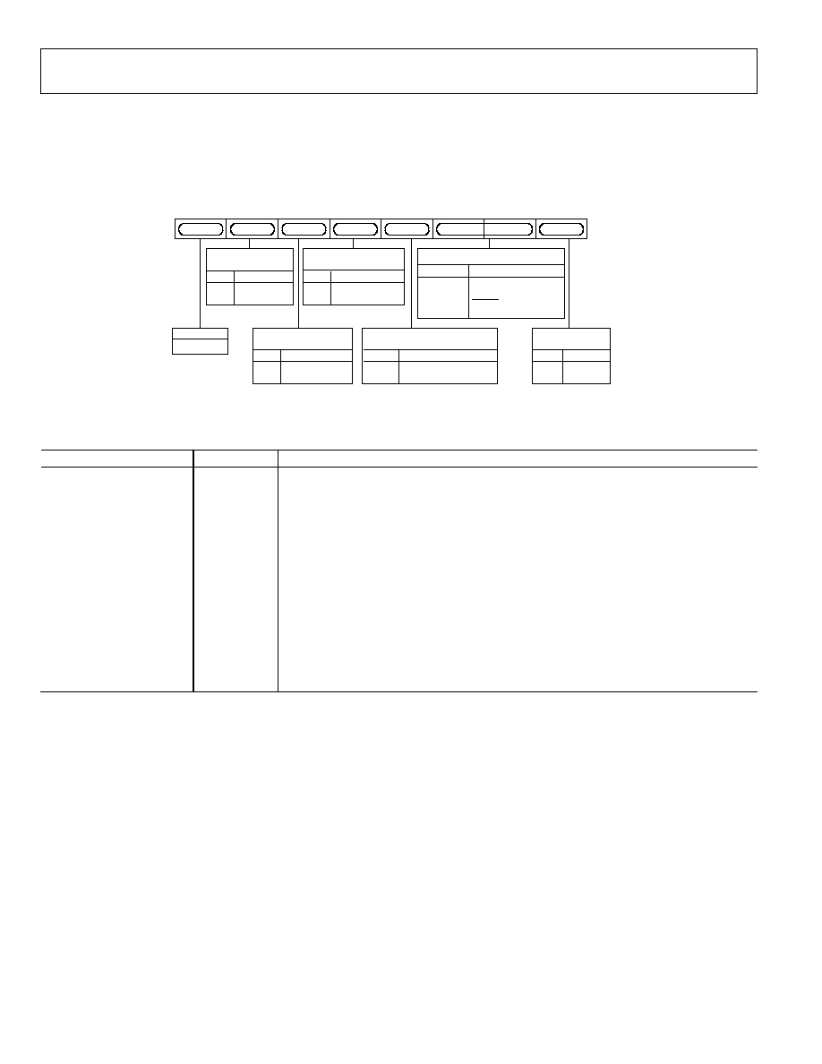
ADV7174/ADV7179
Rev. A | Page 30 of 52
MODE REGISTER 2 (MR2)
Bits:
MR27MR20
Address:
SR4SR0 = 02H
Mode Register 2 is an 8-bit-wide register. Figure 40 shows the various operations under the control of Mode Register 2. This register can
be read from as well as written to.
MR21
MR27
MR22
MR23
MR26
MR25
MR24
MR20
CHROMINANCE
CONTROL
0
ENABLE COLOR
1
DISABLE COLOR
MR24
GENLOCK CONTROL
x
DISABLE GENLOCK
0
ENABLE SUBCARRIER
RESET PIN
1
0
1
1
ENABLE RTC PIN
MR22 MR21
LOW POWER MODE
0
DISABLE
1
ENABLE
MR26
SQUARE PIXEL
CONTROL
0
DISABLE
1
ENABLE
MR20
BURST
CONTROL
0
ENABLE BURST
1
DISABLE BURST
MR25
MR27
ACTIVE VIDEO LINE
DURATION
0
720 PIXELS
1
710 PIXELS/702 PIXELS
MR23
RESERVED
02980-A
-
039
Figure 40. Mode Register 2
Table 11. MR2 Bit Description
Bit Name
Bit No.
Description
Square Pixel Control
MR20
This bit is used to set up square pixel mode. This is available in slave mode only. For NTSC, a
24.5454 MHz clock must be supplied. For PAL, a 29.5 MHz clock must be supplied.
Genlock Control
MR22MR21
These bits control the genlock feature of the ADV7174/ ADV7179. Setting MR21 to Logic 1
configures the SCRESET/RTC pin as an input. Setting MR22 to Logic 0 configures the
SCRESET/RTC pin as a subcarrier reset input. Therefore, the subcarrier will reset to Field 0
following a low-to-high transition on the SCRESET/RTC pin. Setting MR22 to Logic 1 configures
the SCRESET/RTC pin as a real-time control input.
Active Video Line Duration
MR23
This bit switches between two active video line durations. A 0 selects CCIR REC601 (720 pixels
PAL/NTSC), and a 1 selects ITU-R.BT470 standard for active video duration (710 pixels NTSC
and 702 pixels PAL).
Chrominance Control
MR24
This bit enables the color information to be switched on and off the video output.
Burst Control
MR25
This bit enables the burst information to be switched on and off the video output.
Low Power Mode
MR26
This bit enables the lower power mode of the ADV7174/ADV7179. This reduces the DAC
current by 45%.
Reserved
MR27
A Logic 0 must be written to this bit.
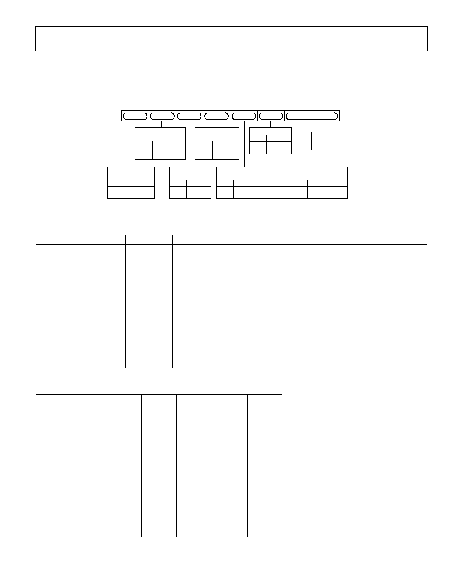
ADV7174/ADV7179
Rev. A | Page 31 of 52
MODE REGISTER 3 (MR3)
Bits:
MR37MR30
Address:
SR4SR0 = 03H
Mode Register 3 is an 8-bit-wide register. Figure 41 shows the various operations under the control of Mode Register 3.
MR31
MR30
MR37
MR32
MR34
MR33
MR35
MR36
MR30
MR31
RESERVED
VBI_OPEN
0
DISABLE
1
ENABLE
MR32
DAC OUTPUT
0
COMPOSITE
1
GREEN/LUMA/Y
MR33
DAC A
BLUE/COMP/Pb
BLUE/COMP/Pb
DAC B
RED/CHROMA/Pr
RED/CHROMA/Pr
DAC C
CHROMA OUTPUT
SELECT
0
DISABLE
1
ENABLE
MR34
TELETEXT
ENABLE
0
DISABLE
1
ENABLE
MR35
TTXREQ BIT
MODE CONTROL
0
NORMAL
1
BIT REQUEST
MR36
INPUT DEFAULT
COLOR
0 DISABLE
1 ENABLE
MR37
02980-A
-
040
Figure 41. Mode Register 3
Table 12. MR3 Bit Description
Bit Name
Bit No.
Description
Revision Code
MR30MR31
These bits are read-only and indicate the revision of the device.
VBI Open
MR32
This bit determines whether or not data in the vertical blanking interval (VBI) is output to
the analog outputs or blanked. VBI data insertion is not available in Slave Mode 0. Also,
when both BLANK input control and VBI open are enabled, BLANK input control has
priority, i.e., VBI data insertion will not work.
DAC Output
MR33
This bit is used to switch the DAC outputs from SCART to a EUROSCART configuration. A
complete list of all DAC output configurations is shown in Table 13.
Chroma Output Select
MR34
With this active high bit it is possible to output an extra chrominance signal C, on DAC A
in any configuration that features a CVBS signal.
Teletext Enable
MR35
This bit must be set to 1 to enable Teletext data insertion on the TTX pin.
TTXREQ Bit Mode Control
MR36
This bit enables switching of the Teletext request signal from a continuous high signal
(MR36 = 0) to a bitwise request signal (MR36 = 1).
Input Default Color
MR37
This bit determines the default output color from the DACs for zero input pixel data (or
disconnected). A Logic 0 means that the color corresponding to 00000000 is displayed. A
Logic 1 forces the output color to black for 00000000 pixel input video data.
Table 13. DAC Output Configuration Matrix
MR34
MR40
MR41
MR33
DAC A
DAC B
DAC C
0
0
0
0
CVBS
CVBS
C
0
0
0
1
Y
CVBS
C
0
0
1
0
CVBS
CVBS
C
0
0
1
1
Y
CVBS
C
0
1
0
0
CVBS
B
R
0
1
0
1
G
B
R
0
1
1
0
CVBS
Pb
Pr
0
1
1
1
Y
Pb
Pr
1
0
0
0
C
CVBS
C
1
0
0
1
Y
CVBS
C
1
0
1
0
C
CVBS
C
1
0
1
1
Y
CVBS
C
1
1
0
0
C
B
R
1
1
0
1
G
B
R
1
1
1
0
C
Pb
Pr
CVBS: Composite Video Baseband Signal
Y: Luminance Component Signal (For YPbPr or Y/C Mode)
C: Chrominance Signal (For Y/C Mode)
Pb: ColorComponent Signal (For YPbPr Mode)
Pr: Color Component Signal (For YPbPr Mode)
R: RED Component Video (For RGB Mode)
G: GREEN Component Video (For RGB Mode)
B: BLUE Component Video (For RGB Mode)
Each DAC can be powered on or off individually
See MR1 Description and Figure 39.
1
1
1
1
Y
Pb
Pr
ADV7174/ADV7179
Rev. A | Page 32 of 52
MODE REGISTER 4 (MR4)
Bits:
MR47MR40
Address:
SR4SR0 = 04H
Mode Register 4 is an 8-bit-wide register. Figure 42 shows the various operations under the control of Mode Register 4.
MR41
MR40
MR47
MR42
MR44
MR43
MR45
MR46
OUTPUT SELECT
0
YC OUTPUT
1
RGB/YPbPr OUTPUT
MR40
RGB SYNC
0
DISABLE
1
ENABLE
MR42
PEDESTAL
CONTROL
0
PEDESTAL OFF
1
PEDESTAL ON
MR44
SLEEP MODE
CONTROL
0
DISABLE
1
ENABLE
MR46
ACTIVE VIDEO
FILTER CONTROL
0
DISABLE
1
ENABLE
MR45
MR47
(0)
ZERO SHOULD
BE WRITTEN TO
THIS BIT
VSYNC_3H
0
DISABLE
1
ENABLE
MR43
RGB/YUV
CONTROL
0
RGB OUTPUT
1
YPbPr OUTPUT
MR41
02980-A
-041
Figure 42. Mode Register 4
Table 14. MR4 Bit Description
Bit Name
Bit No.
Description
Output Select
MR40
This bit specifies if the part is in composite video or RGB/YPbPr mode.
RGB/YPbPr Control
MR41
This bit enables the output from the RGB DACs to be set to YPbPr output video standard.
RGB Sync
MR42
This bit is used to set up the RGB outputs with the sync information encoded on all RGB
outputs.
VSYNC_3H
MR43
When this bit is enabled (1) in slave mode, it is possible to drive the VSYNC active low
input for 2.5 lines in PAL mode and three lines in NTSC mode. When this bit is enabled in
master mode, the ADV7174/ADV7179 outputs an active low VSYNC signal for three lines
in NTSC mode and 2.5 lines in PAL mode.
Pedestal Control
MR44
This bit specifies whether a pedestal is to be generated on the NTSC composite video
signal. This bit is invalid if the ADV7174/ ADV7179 is configured in PAL mode.
Active Video Filter Control
MR45
This bit controls the filter mode applied outside the active video portion of the line. This
filter ensures that the sync rise and fall times are always on spec regardless of which luma
filter is selected. A Logic 1 enables this mode.
Sleep Mode Control
MR46
When this bit is set (1), sleep mode is enabled. With this mode enabled, the
ADV7174/ADV7179 power consumption is reduced to typically 200 nA. The I
2
C registers
can be written to and read from when the ADV7174/ADV7179 is in sleep mode. If MR46 is
set to a (0) when the device is in sleep mode, the ADV7174/ADV7179 comes out of sleep
mode and resumes normal operation. Also, if the RESET signal is applied during sleep
mode, the ADV7174/ADV7179 comes out of sleep mode and resumes normal operation.
Reserved
MR47
A Logic 0 should be written to this bit.
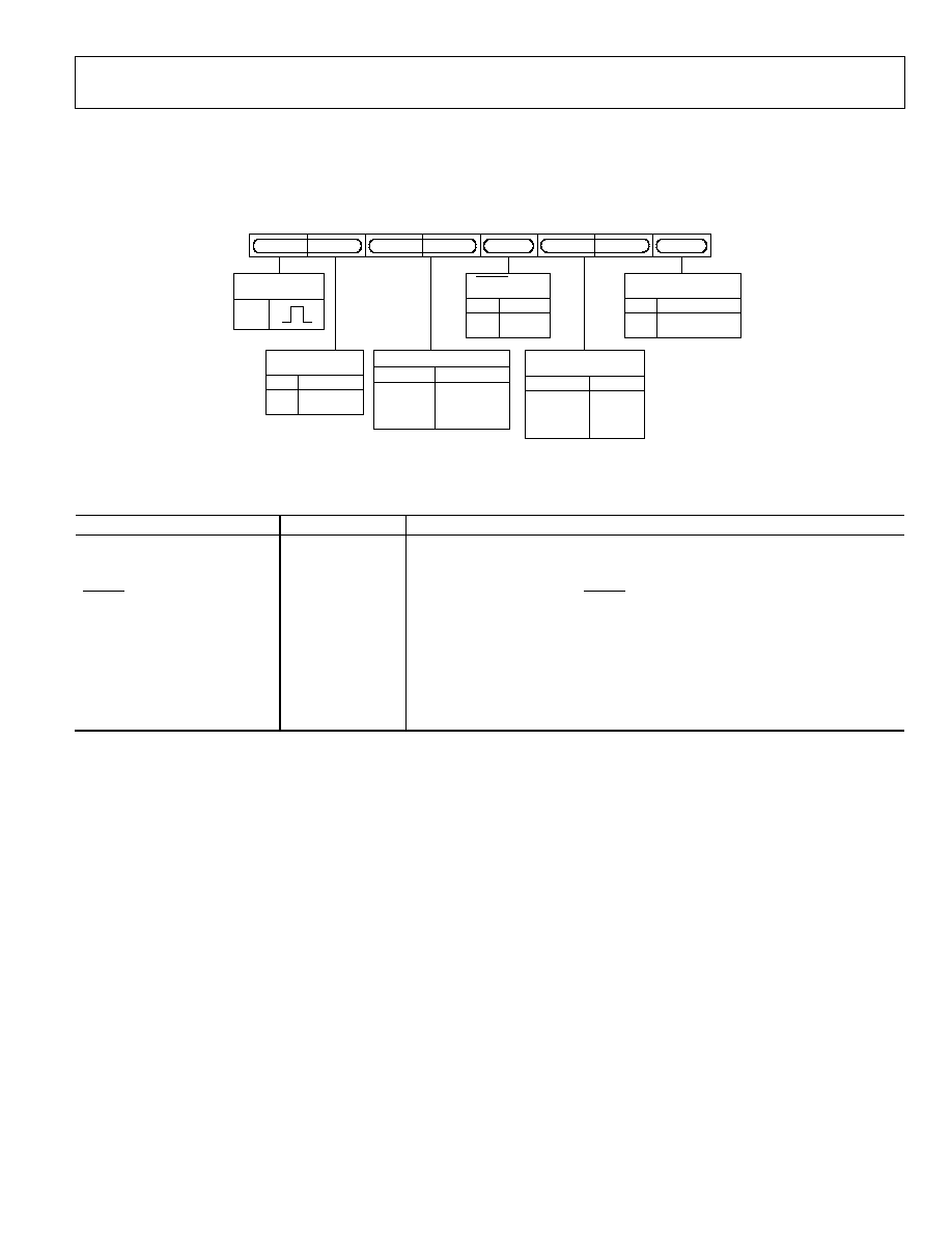
ADV7174/ADV7179
Rev. A | Page 33 of 52
TIMING MODE REGISTER 0 (TR0)
Bits:
TR07TR00
Address:
SR4SR0 = 07H
Figure 43 shows the various operations under the control of Timing Register 0. This register can be read from as well as written to.
TR01
TR00
TR07
TR02
TR03
TR05
TR06
TR04
TIMING
REGISTER RESET
TR07
BLANK INPUT
CONTROL
0
ENABLE
1
DISABLE
TR03
PIXEL PORT
CONTROL
0
8 BIT
1
FORBIDDEN
TR06
MASTER/SLAVE
CONTROL
0
SLAVE TIMING
1
MASTER TIMING
TR00
LUMA DELAY
0
0ns DELAY
0
74ns DELAY
1
148ns DELAY
1
0
1
0
1
222ns DELAY
TR05 TR04
TIMING MODE
SELECTION
0
MODE 0
0
MODE 1
1
MODE 2
1
0
1
0
1
MODE 3
TR02 TR01
02980-A
-
042
Figure 43. Timing Register 0
Table 15. TR0 Bit Description
Bit Name
Bit No.
Description
Master/Slave Control
TR00
This bit controls whether the ADV7174/ADV7179 is in master or slave mode.
Timing Mode Selection
TR02TR01
These bits control the timing mode of the ADV7174/ADV7179. These modes are
described in more detail in the 3.3 V Timing Specifications table.
BLANK Input Control
TR03
This bit controls whether the BLANK input is used when the part is in slave mode.
Luma Delay
TR05TR04
These bits control the addition of a luminance delay. Each bit represents a delay of
74 ns.
Pixel Port Control
TR06
This bit is used to set the pixel port to accept 8-bit or YCrCb data on Pins P7P0.
0 must be written here.
Timing Register Reset
TR07
Toggling the TR07 from low to high and to low again resets the internal timing
counters. This bit should be toggled after power-up, reset, or changing to a new
timing mode.
ADV7174/ADV7179
Rev. A | Page 34 of 52
TIMING MODE REGISTER 1 (TR1)
Bits:
TR17TR10
Address:
SR4SR0 = 08H
Timing Register 1 is an 8-bit-wide register. Figure 44 shows the various operations under the control of Timing Register 1. This register
can be read from as well written to. This register can be used to adjust the width and position of the master mode timing signals.
TR11
TR10
TR17
TR12
TR13
TR15
TR16
TR14
HSYNC TO PIXEL
DATA ADJUST
TR17 TR16
0
0
×
T
PCLK
1
×
T
PCLK
1
×
T
PCLK
4
×
T
PCLK
16
×
T
PCLK
128
×
T
PCLK
0
×
T
PCLK
4
×
T
PCLK
8
×
T
PCLK
16
×
T
PCLK
1
×
T
PCLK
4
×
T
PCLK
16
×
T
PCLK
128
×
T
PCLK
2
×
T
PCLK
3
×
T
PCLK
0
1
1
0
1
0
1
HSYNC TO
FIELD/VSYNC DELAY
TR13 TR12
0
0
1
1
0
1
0
1
HSYNC WIDTH
0
0
1
1
0
1
0
1
TR11 TR10
HSYNC TO FIELD
RISING EDGE DELAY
(MODE 1 ONLY)
x
T
B
T
B
+ 32
µ
s
x
0
1
TR15 TR14
T
C
T
A
T
B
VSYNC WIDTH
(MODE 2 ONLY)
TR15 TR14
0
0
1
1
0
1
0
1
LINE 313
LINE 314
LINE 1
TIMING MODE 1 (MASTER/PAL)
HSYNC
FIELD/VSYNC
T
B
T
A
T
C
02980-A
-
043
Figure 44. Timing Register 1
Table 16. TR1 Bit Description
Bit Name
Bit No.
Description
HSYNC Width
TR11TR10
These bits adjust the HSYNC pulse width.
HSYNC to FIELD/VSYNC
Delay
TR13TR12
These bits adjust the position of the HSYNC output relative to the FIELD/VSYNC output.
HSYNC to FIELD Rising
Edge Delay
TR15TR14
When the ADV7174/ADV7179 is in Timing Mode 1, these bits adjust the position of the HSYNC
output relative to the FIELD output rising edge.
VSYNC Width
TR15TR14
When the ADV7174/ADV7179 is configured in Timing Mode 2, these bits adjust the VSYNC
pulse width.
HSYNC to Pixel Data Adjust TR17TR16
This enables the HSYNC to be adjusted with respect to the pixel data. This allows the Cr and Cb
components to be swapped. This adjustment is available in both master and slave timing modes.
ADV7174/ADV7179
Rev. A | Page 35 of 52
SUBCARRIER FREQUENCY REGISTERS 30
Bits:
FSC3FSC0
Address:
SR4SR00 = 09H0CH
These 8-bit-wide registers are used to set up the subcarrier frequency. The value of these registers is calculated by using the following
equation:
*
2
32
×
Line
Video
One
in
Cycles
Clock
MHz
27
of
No.
Line
Video
of
Line
One
in
Values
Frequency
r
Subcarrie
of
No.
* Rounded to the nearest integer.
For example, in NTSC mode,
Eh
1
C
07
F
21
d
569408542
2
1716
5
.
227
32
=
=
×
=
Value
Frequency
Subcarrier
Note that on power-up, F
SC
Register 0 is set to 16h. A value of 1E as derived above is recommended.
Program as
F
SC
Register 0: 1EH
F
SC
Register 2: 7CH
F
SC
Register 3: F0H
F
SC
Register 4: 21H
Figure 45 shows how the frequency is set up by the four registers.
SUBCARRIER
FREQUENCY
REG 3
SUBCARRIER
FREQUENCY
REG 2
SUBCARRIER
FREQUENCY
REG 1
SUBCARRIER
FREQUENCY
REG 0
FSC30 FSC29
FSC27
FSC25
FSC28
FSC24
FSC31
FSC26
FSC22 FSC21
FSC19
FSC17
FSC20
FSC16
FSC23
FSC18
FSC14 FSC13
FSC11
FSC9
FSC12
FSC8
FSC15
FSC10
FSC6
FSC5
FSC3
FSC1
FSC4
FSC0
FSC7
FSC2
02980-A
-
044
Figure 45. Subcarrier Frequency Register
SUBCARRIER PHASE REGISTER
Bits:
FP7FP0
Address:
SR4SR0 = 0DH
This 8-bit-wide register is used to set up the subcarrier phase. Each bit represents 1.41°. For normal operation, this register is set to 00H.
CLOSED CAPTIONING EVEN FIELD DATA REGISTERS 10
Bits:
CED15CED0
Address:
SR4SR0 = 0EH0FH
These 8-bit-wide registers are used to set up the closed captioning extended data bytes on even fields. Figure 46 shows how the high and
low bytes are set up in the registers.
BYTE 1
BYTE 0
CED6
CED5
CED3
CED1
CED4
CED2
CED0
CED7
CED14 CED13
CED11
CED9
CED12
CED10
CED8
CED15
002980-A
-
045
Figure 46. Closed Captioning Extended Data Register
ADV7174/ADV7179
Rev. A | Page 36 of 52
CLOSED CAPTIONING ODD FIELD DATA REGISTERS 10
Bits:
CCD15CCD0
Subaddress:
SR4SR0 = 10H11H
These 8-bit-wide registers are used to set up the closed captioning data bytes on odd fields. Figure 47 shows how the high and low bytes
are set up in the registers.
BYTE 1
BYTE 0
CCD6
CCD5
CCD3
CCD1
CCD4
CCD2
CCD0
CCD7
CCD14 CCD13
CCD11
CCD9
CCD12
CCD10
CCD8
CCD15
002980-A
-
046
Figure 47. Closed Captioning Data Register
NTSC PEDESTAL/PAL TELETEXT CONTROL REGISTERS 30
Bits:
PCE15PCE0, PCO15PCO0/TXE15TXE0, TXO15TXO0
Subaddress:
SR4SR0 = 12H15H
These 8-bit-wide registers are used to enable the NTSC pedestal/ PAL Teletext on a line-by-line basis in the vertical blanking interval for
both odd and even fields. Figure 48 and Figure 49 show the four control registers. A Logic 1 in any of the bits of these registers has the
effect of turning the pedestal off on the equivalent line when used in NTSC. A Logic 1 in any of the bits of these registers has the effect of
turning Teletext on the equivalent line when used in PAL.
FIELD 1/3
PCO6
PCO5
PCO3
PCO1
PCO4
PCO2
PCO0
PCO7
LINE 17 LINE 16 LINE 15 LINE 14 LINE 13 LINE 12 LINE 11 LINE 10
PCO14 PCO13
PCO11
PCO9
PCO12
PCO10
PCO8
PCO15
LINE 25 LINE 24 LINE 23 LINE 22 LINE 21 LINE 20 LINE 19 LINE 18
FIELD 1/3
FIELD 2/4
PCE6
PCE5
PCE3
PCE1
PCE4
PCE2
PCE0
PCE7
LINE 17 LINE 16 LINE 15 LINE 14 LINE 13 LINE 12 LINE 11 LINE 10
PCE14 PCE13
PCE11
PCE9
PCE12
PCE10
PCE8
PCE15
LINE 25 LINE 24 LINE 23 LINE 22 LINE 21 LINE 20
LINE 19 LINE 18
FIELD 2/4
02980-A
-
047
Figure 48. Pedestal Control Registers
FIELD 1/3
FIELD 1/3
FIELD 2/4
FIELD 2/4
TXO6
TXO5
TXO3
TXO1
TXO4
TXO2
TXO0
TXO7
LINE 14 LINE 13 LINE 12 LINE 11 LINE 10 LINE 9
LINE 8 LINE 7
TXO14
TXO13
TXO11
TXO9
TXO12
TXO10
TXO8
TXO15
LINE 22 LINE 21 LINE 20 LINE 19 LINE 18 LINE 17 LINE 16 LINE 15
TXE6
TXE5
TXE3
TXE1
TXE4
TXE2
TXE0
TXE7
TXE14
TXE13
TXE11
TXE9
TXE12
TXE10
TXE8
TXE15
LINE 14 LINE 13 LINE 12 LINE 11 LINE 10 LINE 9
LINE 8 LINE 7
LINE 22 LINE 21 LINE 20 LINE 19 LINE 18 LINE 17 LINE 16 LINE 15
02980-A
-
048
Figure 49. Teletext Control Registers
ADV7174/ADV7179
Rev. A | Page 37 of 52
TELETEXT REQUEST CONTROL REGISTER (TC07)
Bits:
TC07TC00
Address:
SR4SR0 = 19H
Teletext control register is an 8-bit-wide register (see Figure 50).
Table 17. Teletext Request Control Register
Bit Name
Bit No.
Description
TTXREQ Rising Edge Control
TC07TC04
These bits control the position of the rising edge of TTXREQ. It can be
programmed from 0 CLOCK cycles to a maximum of 15 CLOCK cycles (see
Figure 50).
TTXREQ Falling Edge Control
TC03TC00
These bits control the position of the falling edge of TTXREQ. It can be
programmed from zero CLOCK cycles to a max of 15 CLOCK cycles. This controls
the active window for Teletext data. Increasing this value reduces the amount of
Teletext bits below the default of 360. If Bits TC03TC00 are 00H when Bits TC07
TC04 are changed, the falling edge of TTXREQ tracks that of the rising edge, i.e.,
the time between the falling and rising edge remains constant (see Figure 49).
CGMS_WSS REGISTER 0 (C/W0)
Bits:
C/W07C/W00
Address:
SR4SR0 = 16H
CGMS_WSS Register 0 is an 8-bit-wide register. Figure 51 shows the operations under the control of this register.
TC01
TC00
TC07
TC02
TC04
TC03
TC05
TC06
TTXREQ RISING EDGE CONTROL
TC07 TC06 TC05 TC04
0
0
0
0
0 PCLK
0
0
0
1
1
1
1
1
1
1
1
0
"
"
"
"
1 PCLK
" PCLK
14 PCLK
15 PCLK
TTXREQ FALLING EDGE CONTROL
TC03 TC02 TC01 TC00
0 PCLK
1 PCLK
" PCLK
14 PCLK
15 PCLK
0
0
0
0
0
0
0
1
1
1
1
1
1
1
1
0
"
"
"
"
02980-A
-
049
Figure 50. Teletext Control Register
C/W07
C/W06
C/W05
C/W04
C/W03
C/W02
C/W01
C/W00
C/W07
WIDE SCREEN
SIGNAL CONTROL
0
DISABLE
1
ENABLE
0
DISABLE
1
ENABLE
C/W05
CGMS ODD FIELD
CONTROL
C/W06
CGMS EVEN FIELD
CONTROL
0
DISABLE
1
ENABLE
C/W04
CGMS CRC CHECK
CONTROL
0
DISABLE
1
ENABLE
C/W03 C/W00
CGMS DATA BITS
02980-A
-
050
Figure 51. CGMS_WSS Register 0
Table 18. C/W0 Bit Description
Bit Name
Bit No.
Description
CGMS Data Bits
C/W03C/W00
These four data bits are the final four bits of the CGMS data output stream. Note it is
CGMS data ONLY in these bit positions, i.e., WSS data does not share this location.
CGMS CRC Check Con
t
rol
C/W04
When this bit is enabled (1), the last six bits of the CGMS data, i.e., the CRC check
sequence, are calculated internally by the ADV7174/ADV7179. If this bit is disabled (0), the
CRC values in the register are output to the CGMS data stream.
CGMS Odd Field Control
C/W05
When this bit is set (1), CGMS is enabled for odd fields. Note this is only valid in NTSC mode.
CGMS Even Field Control
C/W06
When this bit is set (1), CGMS is enabled for even fields. Note this is only valid in NTSC mode.
WSS Control
C/W07
When this bit is set (1), wide screen signaling is enabled. Note this is only valid in PAL mode.
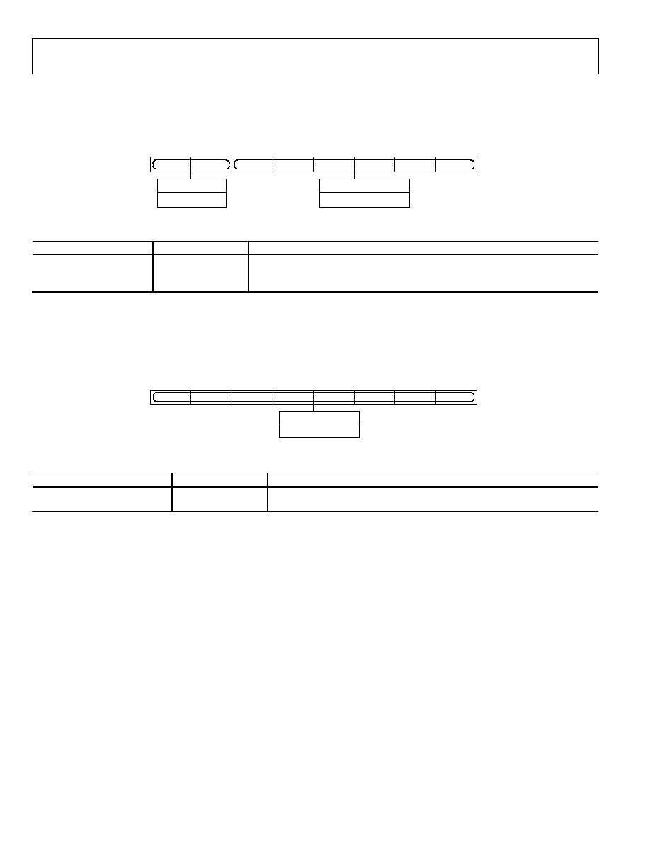
ADV7174/ADV7179
Rev. A | Page 38 of 52
CGMS_WSS REGISTER 1 (C/W1)
Bits:
C/W17C/W10
Address :
SR4SR0 = 17H
CGMS_WSS Register 1 is an 8-bit-wide register. Figure 52 shows the operations under the control of this register.
C/W17
C/W16
C/W15
C/W14
C/W13
C/W12
C/W11
C/W10
C/W15 C/W10
CGMS/WSS DATA BITS
C/W17 C/W16
CGMS DATA BITS
02980-A
-
051
Figure 52. CGMS_WSS Register 1
Table 19. C/W1 Bit Description
Bit Name
Bit No.
Description
CGMS/WSS Data Bits
C/W15C/W10
These bit locations are shared by CGMS data and WSS data. In NTSC mode, these bits
are CGMS data. In PAL mode, these bits are WSS data.
CGMS Data Bits
C/W17C/W16
These bits are CGMS data bits only.
CGMS_WSS REGISTER 2 (C/W2)
Bits:
C/W27C/W20
Address:
(SR4SR00) = 18H
CGMS_WSS Register 2 is an 8-bit-wide register. Figure 53 shows the operations under the control of this register.
C/W27
C/W26
C/W25
C/W24
C/W23
C/W22
C/W21
C/W20
C/W27 C/W20
CGMS/WSS DATA BITS
02980-A
-
052
Figure 53. CGMS_WSS Register 2
Table 20. C/W2 Bit Description
Bit Name
Bit No.
Description
CGMS/WSS Data Bits
C/W27C/W20
These bit locations are shared by CGMS data and WSS data. In NTSC mode, these
bits are CGMS data. In PAL mode, these bits are WSS data.
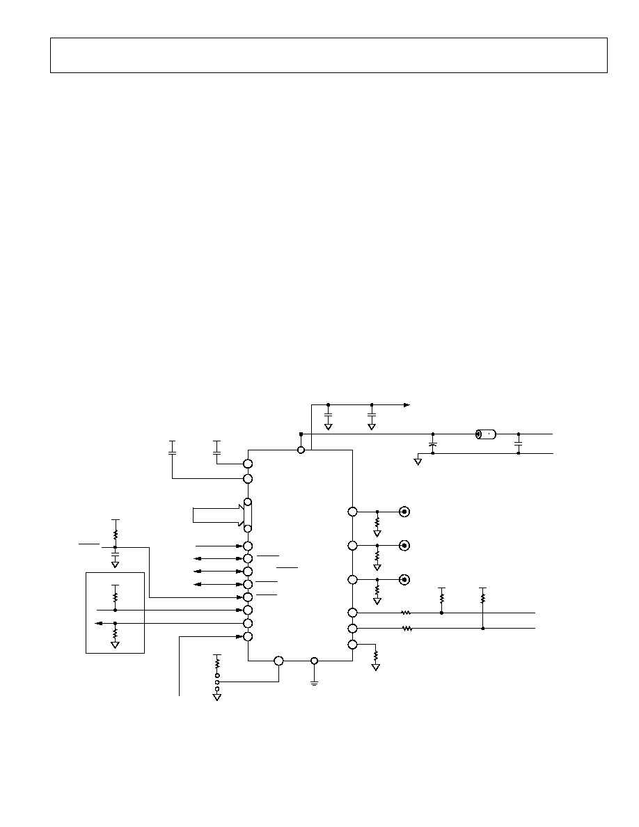
ADV7174/ADV7179
Rev. A | Page 39 of 52
APPENDIX 1--BOARD DESIGN AND LAYOUT CONSIDERATIONS
The ADV7174/ADV7179 is a highly integrated circuit contain-
ing both precision analog and high speed digital circuitry. It has
been designed to minimize interference effects on the integrity
of the analog circuitry by the high speed digital circuitry. It is
imperative that these same design and layout techniques be
applied to the system-level design so that high speed, accurate
performance is achieved. Figure 54 shows the analog interface
between the device and monitor.
The layout should be optimized for lowest noise on the
ADV7174/ADV7179 power and ground lines by shielding the
digital inputs and providing good decoupling. The lead length
between groups of V
AA
and GND pins should be minimized to
reduce inductive ringing.
GROUND PLANES
The ground plane should encompass all ADV7174/ADV7179
ground pins, voltage reference circuitry, power supply bypass
circuitry for the ADV7174/ADV7179, the analog output traces,
and all the digital signal traces leading up to the ADV7174/
ADV7179. The ground plane is the board's common ground
plane.
POWER PLANES
The ADV7174/ADV7179 and any associated analog circuitry
should have its own power plane, referred to as the analog
power plane (V
AA
). This power plane should be connected to
the regular PCB power plane (V
CC
) at a single point through a
ferrite bead. This bead should be located within 3 inches of the
ADV7174/ADV7179.
The metallization gap separating the device power plane and
board power plane should be as narrow as possible to minimize
the obstruction to the flow of heat from the device into the
general board.
The PCB power plane should provide power to all digital logic
on the PC board, and the analog power plane should provide
power to all ADV7174/ADV7179 power pins and voltage
reference circuitry.
Plane-to-plane noise coupling can be reduced by ensuring that
portions of the regular PCB power and ground planes do not
overlay portions of the analog power plane unless they can be
arranged so that the plane-to-plane noise is common mode.
L1
(FERRITE BEAD)
5k
3.3 V (V
CC
)
150
5k
3.3 V (V
CC
)
MPU BUS
35, 3539
0.1
µ
F
0.01
µ
F
0.1
µ
F
3.3 V (V
AA
)
0.1
µ
F
3.3V (V
AA
)
10k
3.3 V (V
AA
)
27MHz CLOCK
(SAME CLOCK AS USED BY
MPEG2 DECODER)
POWER SUPPLY DECOUPLING
FOR EACH POWER SUPPLY GROUP
10
µ
F
33
µ
F
GND
3.3 V
(V
CC
)
GND
ALSB
HSYNC
FIELD/VSYNC
BLANK
RESET
CLOCK
R
SET
SDATA
SCLOCK
DAC B
DAC C
V
AA
V
REF
COMP
P7P0
3.3 V (V
AA
)
75
75
75
SCRESET/RTC
ADV7174/ADV7179
UNUSED
INPUTS
SHOULD BE
GROUNDED
DAC A
100
100
RESET
TTX
TTXREQ
100k
100k
3.3 V (V
CC
)
TTX
TTXREQ
TELETEXT PULL-UP AND
PULL-DOWN RESISTORS
SHOULD ONLY BE USED
IF THESE PINS ARE NOT
CONNECTED
4k
3.3 V (V
AA
)
100nF
24
28
29
21
22
31
16
1
30
32
23
13
14
15
20
34
33
02980-A
-
053
Figure 54. Recommended Analog Circuit Layout
ADV7174/ADV7179
Rev. A | Page 40 of 52
SUPPLY DECOUPLING
For optimum performance, bypass capacitors should be in-
stalled using the shortest leads possible, consistent with reliable
operation, to reduce the lead inductance. Best performance is
obtained with 0.1 µF ceramic capacitor decoupling. Each group
of V
AA
pins on the ADV7174/ADV7179 must have at least one
0.1 µF decoupling capacitor to GND. These capacitors should be
placed as close to the device as possible.
It is important to note that while the ADV7174/ADV7179
contains circuitry to reject power supply noise, this rejection
decreases with frequency. If a high frequency switching power
supply is used, the designer should pay close attention to
reducing power supply noise and consider using a 3-terminal
voltage regulator for supplying power to the analog power
plane.
DIGITAL SIGNAL INTERCONNECT
The digital inputs to the ADV7174/ADV7179 should be isolated
as much as possible from the analog outputs and other analog
circuitry. Also, these input signals should not overlay the analog
power plane.
Due to the high clock rates involved, long clock lines to the
ADV7174/ADV7179 should be avoided to reduce noise pickup.
Any active termination resistors for the digital inputs should be
connected to the regular PCB power plane (V
CC
) and not to the
analog power plane.
ANALOG SIGNAL INTERCONNECT
The ADV7174/ADV7179 should be located as close to the
output connectors as possible to minimize noise pickup and
reflections due to impedance mismatch.
The video output signals should overlay the ground plane, not
the analog power plane, to maximize the high frequency power
supply rejection.
Digital inputs, especially pixel data inputs and clocking signals,
should never overlay any of the analog signal circuitry and
should be kept as far away as possible.
For best performance, the outputs should each have a 75 load
resistor connected to GND. These resistors should be placed as
close as possible to the ADV7174/ADV7179 to minimize
reflections.
The ADV7174/ADV7179 should have no inputs left floating.
Any inputs that are not required should be tied to ground.
The circuit in Figure 55 can be used to generate a 13.5 MHz
waveform using the 27 MHz clock and the HSYNC pulse. This
waveform is guaranteed to produce the 13.5 MHz clock in
synchronization with the 27 MHz clock. This 13.5 MHz clock
can be used if the 13.5 MHz clock is required by the MPEG
decoder. This guarantees that the Cr and Cb pixel information
is input to the ADV7174/ADV7179 in the correct sequence.
Note that the exposed metal paddle on the bottom side of the
LFCSP package must be soldered to PCB ground for proper
heat dissipation and also for electrical noise and mechanical
strength benefits.
D
Q
CK
D
Q
CK
CLOCK
HSYNC
13.5MHz
02980-A
-
054
Figure 55. Circuit to Generate 13.5 MHz
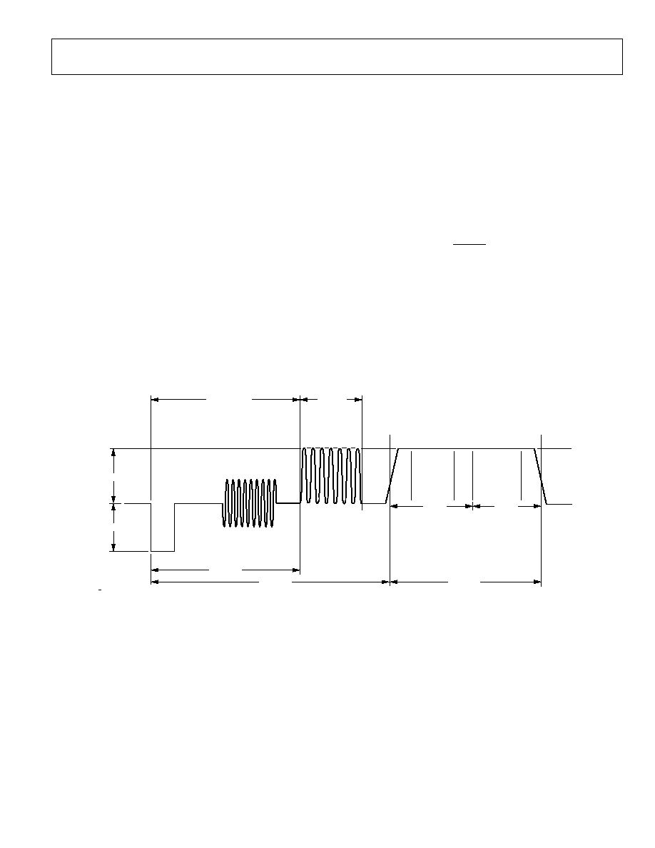
ADV7174/ADV7179
Rev. A | Page 41 of 52
APPENDIX 2--CLOSED CAPTIONING
The ADV7174/ADV7179 supports closed captioning, conform-
ing to the standard television synchronizing waveform for color
transmission. Closed captioning is transmitted during the
blanked active line time of Line 21 of the odd fields and Line
284 of even fields.
Closed captioning consists of a 7-cycle sinusoidal burst that is
frequency-locked and phase-locked to the caption data. After
the clock run-in signal, the blanking level is held for 2 data bits
and is followed by a Logic 1 start bit. 16 bits of data follow the
start bit. These consist of two 8-bit bytes, 7 data bits, and 1 odd
parity bit. The data for these bytes is stored in closed captioning
Data Registers 0 and 1.
The ADV7174/ADV7179 also supports the extended closed
captioning operation, which is active during even fields, and is
encoded on scan Line 284. The data for this operation is stored
in closed captioning extended Data Registers 0 and 1.
All clock run-in signals and timing to support closed captioning
on Lines 21 and 284 are automatically generated by the
ADV7174/ADV7179. All pixel inputs are ignored during Lines
21 and 284. FCC Code of Federal Regulations (CFR) 47 Section
15.119 and EIA-608 describe the closed captioning information
for Lines 21 and 284.
The ADV7174/ADV7179 uses a single buffering method. This
means that the closed captioning buffer is only one byte deep,
therefore there will be no frame delay in outputting the closed
captioning data unlike other 2-byte deep buffering systems. The
data must be loaded at least one line before (Line 20 or Line 283)
it is outputted on Line 21 and Line 284. A typical implementation
of this method is to use VSYNC to interrupt a microprocessor,
which in turn loads the new data (two bytes) every field. If no
new data is required for transmission, you must insert zeros in
both the data registers; this is called nulling. It is also important
to load control codes, all of which are double bytes, on Line 21,
or a TV cannot recognize them. If you have a message such as
"Hello World," which has an odd number of characters, it is
important to pad it out to an even number to get the end of the
caption 2-byte control code to land in the same field.
50 IRE
12.91
µ
s
S
T
A
R
T
P
A
R
I
T
Y
P
A
R
I
T
Y
D0D6
D0D6
10.003
µ
s
33.764
µ
s
40 IRE
FREQUENCY = F
SC
= 3.579545MHz
AMPLITUDE = 40 IRE
REFERENCE COLOR BURST
(9 CYCLES)
7 CYCLES
OF 0.5035 MHz
(CLOCK RUN-IN)
10.5 ± 0.25
µ
s
TWO 7-BIT + PARITY
ASCII CHARACTERS
(DATA)
27.382
µ
s
BYTE 0
BYTE 1
02980-A
-
055
Figure 56. Closed Captioning Waveform (NTSC)
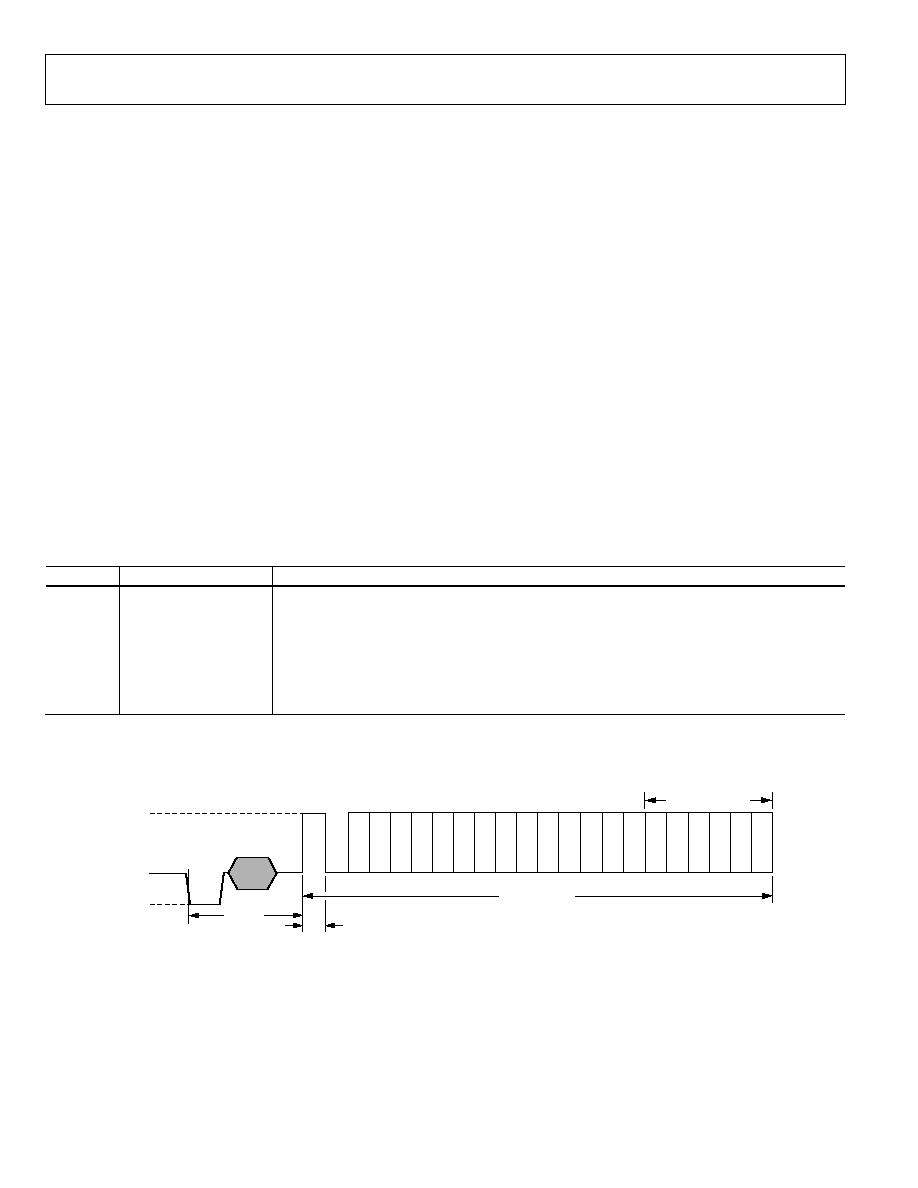
ADV7174/ADV7179
Rev. A | Page 42 of 52
APPENDIX 3--COPY GENERATION MANAGEMENT SYSTEM (CGMS)
The ADV7174/ADV7179 supports the CGMS, conforming to
the standard. CGMS data is transmitted on Line 20 of the odd
fields and on Line 283 of the even fields. Bits C/W05 and
C/W06 control whether or not CGMS data is output on odd
and even fields. CGMS data can only be transmitted when the
ADV7174/ ADV7179 is configured in NTSC mode. The CGMS
data is 20 bits long, the function of each of these bits is as shown
below. The CGMS data is preceded by a reference pulse of the
same amplitude and duration as a CGMS bit (see Figure 57).
The bits are output from the configuration registers in the
following order: C/W00 = C16, C/W01 = C17, C/W02 = C18,
C/W03 = C19, C/W10 = C8, C/ W11 = C9, C/W12 = C10,
C/W13 = C11, C/W14 = C12, C/ W15 = C13, C/W16 = C14,
C/W17 = C15, C/W20 = C0, C/W21 = C1, C/W22 = C2, C/W23
= C3, C/W24 = C4, C/W25 = C5, C/W26 = C6, C/W27 = C7. If
Bit C/W04 is set to a Logic 1, the last six bits, C19C14, which
comprise the 6-bit CRC check sequence, are calculated
automatically on the ADV7174/ADV7179 based on the lower
14 bits (C0C13) of the data in the data registers and output
with the remaining 14 bits to form the complete 20 bits of the
CGMS data. The calculation of the CRC sequence is based on
the polynomial X
6
+ X + 1 with a preset value of 111111. If
C/W04 is set to a Logic 0, all 20 bits (C0C19) are directly
output from the CGMS registers (no CRC is calculated; it must
be calculated by the user).
FUNCTION OF CGMS BITS
Word 0 6 Bits
Word 1 4 Bits
Word 2 4 Bits
CRC 6 Bits CRC Polynomial = X
6
+ X + 1 (Preset to 111111)
Table 21. Bit 1Bit 14
Word Bit
Function
Word 0
1
0
B1
Aspect
Ratio 16:9
4:3
B2
Display
Format
Letterbox
Normal
B3
Undefined
B4, B5, B6
Identification information about video and other signals, for example, audio
Word 1
B7, B8, B9, B10
Identification signal incidental to Word 0
Word 2
B11, B12, B13, B14
Identification signal and information incidental to Word 0
CRC SEQUENCE
11.2
µ
s
2.235
µ
s ± 20ns
49.1
µ
s ± 0.5
µ
s
REF
C0 C1 C2 C3 C4 C5 C6 C7 C8 C9 C10 C11 C12 C13 C14 C15 C16 C17 C18 C19
100 IRE
70 IRE
0 IRE
40 IRE
02980-A
-
056
Figure 57. CGMS Waveform Diagram
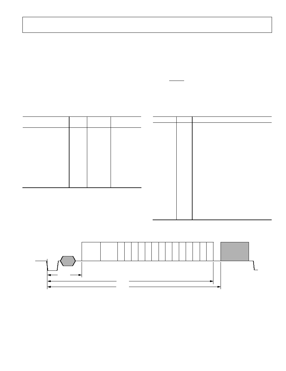
ADV7174/ADV7179
Rev. A | Page 43 of 52
APPENDIX 4--WIDE SCREEN SIGNALING (WSS)
The ADV7174/ADV7179 supports WSS, conforming to the
standard. WSS data is transmitted on Line 23. WSS data can
only be transmitted when the ADV7174/ ADV7179 is
configured in PAL mode. The WSS data is 14 bits long, the
function of each of these bits is as shown below. The WSS data
is preceded by a run-in sequence and a start code (see Figure 58).
The bits are output from the configuration registers in the
following order: C/W20 = W0, C/W21 = W1, C/W22 = W2,
C/W23 = W3, C/W24 = W4, C/W25 = W5, C/W26 = W6,
C/W27 = W7, C/W10 = W8, C/W11 = W9, C/W12 = W10,
C/W13 = W11, C/W14 = W12, C/W15 = W13. If the Bit C/W07
is set to a Logic 1, it enables the WSS data to be transmitted on
Line 23. The latter portion of Line 23 (42.5 µs from the falling
edge of HSYNC) is available for the insertion of video.
FUNCTION OF WSS BITS
Table 22. Bit 0Bit 2 Bit 3 is the odd parity check of Bit 0Bit 2
B0 B1 B2 B3
Aspect
Ratio Format Position
0 0 0 1 4:3 Full
Format
Not
Applicable
1 0 0 0 14:9 Letterbox
Center
0 1 0 0 14:9 Letterbox
Top
1 1 0 1 16:9 Letterbox
Center
0 0 1 0 16:9 Letterbox
Top
1 0 1 1 >16:9 Letterbox
Center
0 1 1 1 14:9 Full
Format
Center
1 1 1 0 16:9 Not
Applicable
Not
Applicable
Table 23. Bit 4Bit 7
Bit Value
Description
B4 0
1
Camera Mode
Film Mode
B5 0
1
Standard Coding
Motion Adaptive Color Plus
B6 0
1
No Helper
Modulated Helper
B7
Reserved
B8 0
1
No Teletext Subtitles
Teletext Subtitles
B9B10
0, 0
No Open Subtitles
1, 0
Subtitles in Active Image Area
0, 1
Subtitles out of Active Image Area
1,
1
Reserved
B11 0
1
No Surround Sound Information
Surround Sound Mode
B12 Reserved
B13 Reserved
11.0
µ
s
W0 W1 W2 W3 W4 W5 W6 W7 W8 W9 W10 W11 W12 W13
500mV
RUN-IN
SEQUENCE
START
CODE
ACTIVE
VIDEO
38.4
µ
s
42.5
µ
s
02980-A
-
057
Figure 58. WSS Waveform Diagram
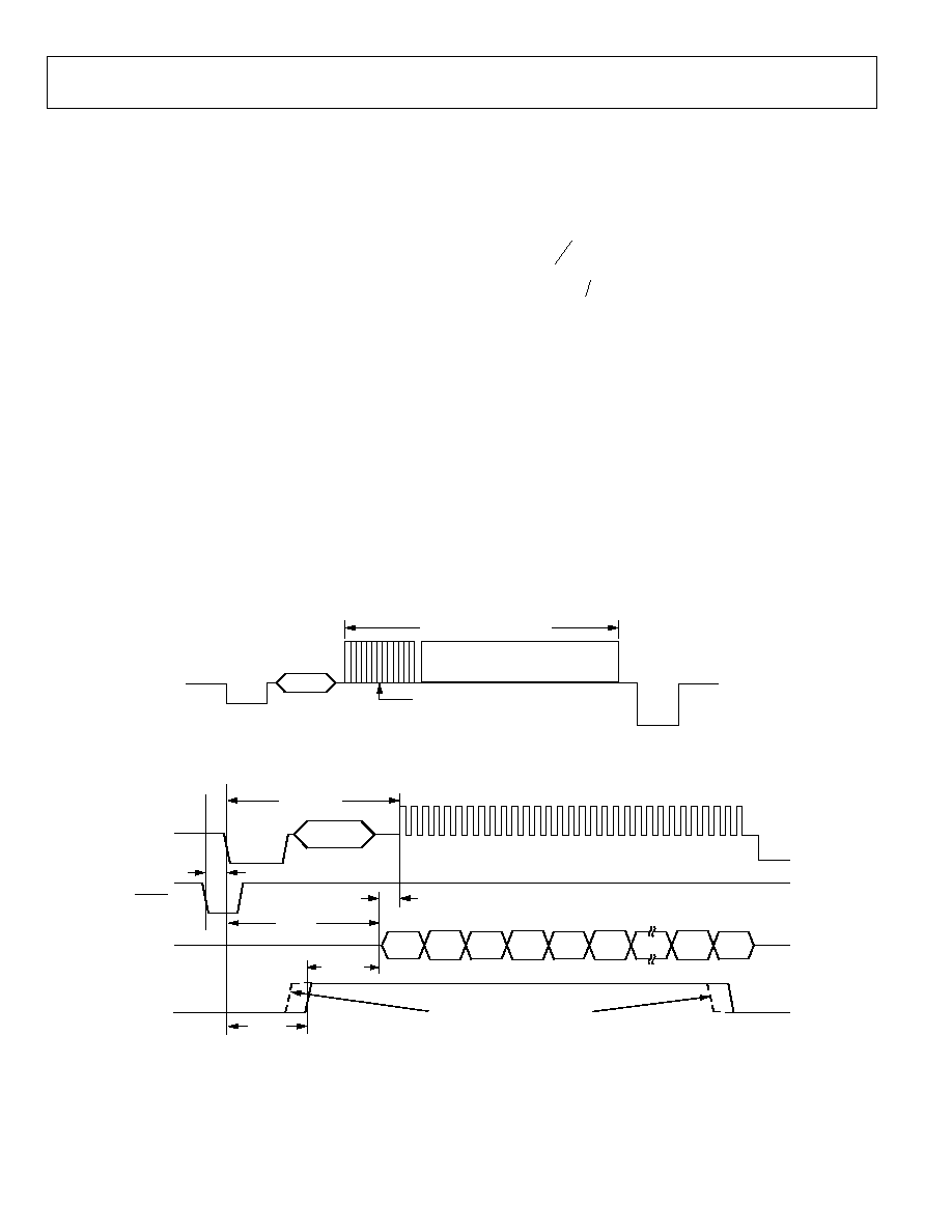
ADV7174/ADV7179
Rev. A | Page 44 of 52
APPENDIX 5--TELETEXT
TELETEXT INSERTION
t
PD
is the time needed by the ADV7174/ADV7179 to interpolate
input data on TTX and insert it onto the CVBS or Y outputs,
such that it appears t
SYNTTXOUT
= 10.2 µs after the leading edge of
the horizontal signal. Time TTX
DEL
is the pipeline delay time by
the source that is gated by the TTXREQ signal in order to
deliver TTX data.
With the programmability offered with the TTXREQ signal on
the rising/falling edges, the TTX data is always inserted at the
correct position of 10.2 µs after the leading edge of horizontal
sync pulse, thus enabling a source interface with variable pipe-
line delays.
The width of the TTXREQ signal must always be maintained to
allow the insertion of 360 (to comply with the Teletext standard
PAL-WST) Teletext bits at a text data rate of 6.9375 Mbits/s.
This is achieved by setting TC03TC00 to 0. The insertion
window is not open if the Teletext enable bit (MR35) is set to 0.
TELETEXT PROTOCOL
The relationship between the TTX bit clock (6.9375 MHz) and
the system clock (27 MHz) for 50 Hz is
(
)
027777
.
1
10
75
.
6
10
9375
.
6
75
.
6
4
6
6
27
=
×
×
=
MHz
MHz
Thus, 37 TTX bits correspond to 144 clocks (27 MHz) and each
bit has a width of almost four clock cycles. The ADV7174/
ADV7179 uses an internal sequencer and variable phase inter-
polation filter to minimize the phase jitter and thus generate a
band-limited signal that can be output on the CVBS and Y
outputs.
At the TTX input, the bit duration scheme repeats after every 37
TTX bits or 144 clock cycles. The protocol requires that TTX
Bits 10, 19, 28, and 37 are carried by three clock cycles and all
other bits by four clock cycles. After 37 TTX bits, the next bits
with three clock cycles are 47, 56, 65, and 74. This scheme holds
for all following cycles of 37 TTX bits until all 360 TTX bits are
completed. All Teletext lines are implemented in the same way.
Individual control of Teletext lines is controlled by Teletext
setup registers.
ADDRESS AND DATA
RUN-IN CLOCK
TELETEXT VBI LINE
45 BYTES (360 BITS) PAL
02980-A
-
058
Figure 59. Teletext VBI Line
PROGRAMMABLE PULSE EDGES
t
PD
t
PD
CVBS/Y
HSYNC
TTXREQ
TTX
DATA
t
SYNTTXOUT
= 10.2
µ
s
t
PD
= PIPELINE DELAY THROUGH ADV7174/ADV7179
TTX
DEL
= TTXREQ TO TTX (PROGRAMMABLE RANGE = 4 BITS [015 CLOCK CYCLES])
t
SYNTTXOUT
10.2
µ
s
TTX
DEL
TTX
ST
02980-A
-
059
Figure 60. Teletext Functionality
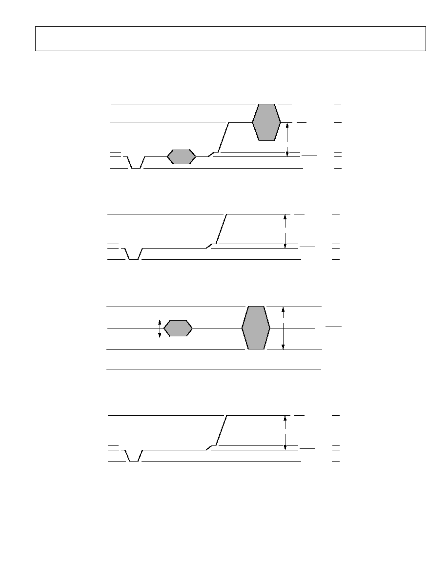
ADV7174/ADV7179
Rev. A | Page 45 of 52
APPENDIX 6--WAVEFORMS
NTSC WAVEFORMS (WITH PEDESTAL)
130.8 IRE
100 IRE
7.5 IRE
0 IRE
40 IRE
PEAK COMPOSITE
REF WHITE
SYNC LEVEL
BLANK LEVEL
1268.1mV
1048.4mV
387.6mV
334.2mV
48.3mV
714.2mV
BLACK LEVEL
02980-A
-
060
Figure 61. NTSC Composite Video Levels
100 IRE
7.5 IRE
0 IRE
40 IRE
REF WHITE
SYNC LEVEL
BLANK LEVEL
1048.4mV
387.6mV
334.2mV
48.3mV
BLACK LEVEL
714.2mV
02980-A
-
061
Figure 62. NTSC Luma Video Levels
650mV
335.2mV
963.8mV
0mV
PEAK CHROMA
BLANK/BLACK LEVEL
286mV (p-p)
PEAK CHROMA
629.7mV (p-p)
02980-A
-
062
Figure 63. NTSC Chroma Video Levels
100 IRE
7.5 IRE
0 IRE
40 IRE
REF WHITE
SYNC LEVEL
BLANK LEVEL
1052.2mV
387.5mV
331.4mV
45.9mV
720.8mV
BLACK LEVEL
02980-A
-
063
Figure 64. NTSC RGB Video Levels
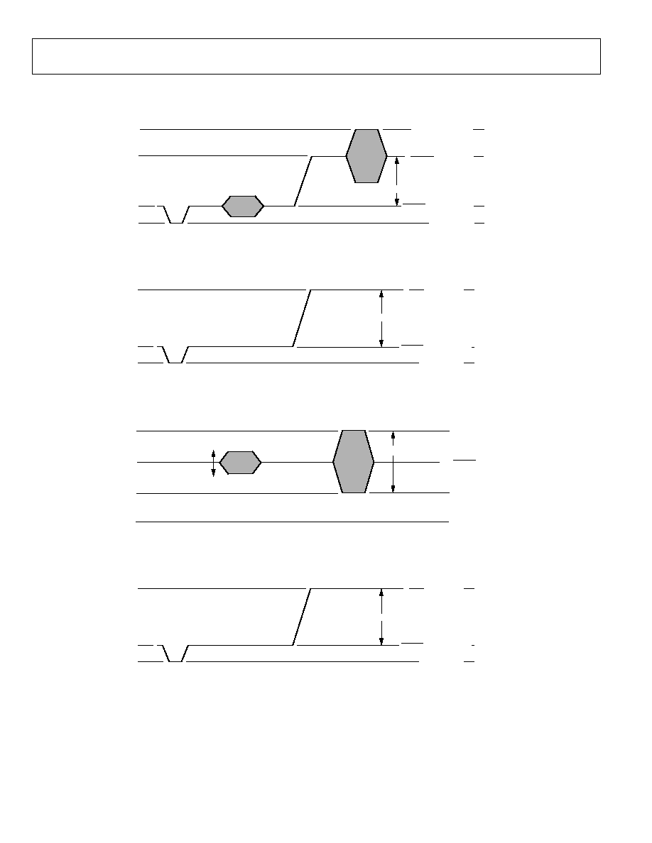
ADV7174/ADV7179
Rev. A | Page 46 of 52
NTSC WAVEFORMS (WITHOUT PEDESTAL)
130.8 IRE
100 IRE
0 IRE
40 IRE
PEAK COMPOSITE
REF WHITE
SYNC LEVEL
BLANK/BLACK LEVEL
1289.8mV
1052.2mV
338mV
52.1mV
714.2mV
02980-A
-
064
Figure 65. NTSC Composite Video Levels
100 IRE
0 IRE
40 IRE
REF WHITE
SYNC LEVEL
BLANK/BLACK LEVEL
1052.2mV
338mV
52.1mV
714.2mV
02980-A
-
065
Figure 66. NTSC Luma Video Levels
650mV
299.3mV
978mV
0mV
PEAK CHROMA
BLANK/BLACK LEVEL
286mV (p-p)
PEAK CHROMA
694.9mV (p-p)
02980-A
-
066
Figure 67. NTSC Chroma Video Levels
100 IRE
0 IRE
40 IRE
REF WHITE
SYNC LEVEL
BLANK/BLACK LEVEL
715.7mV
1052.2mV
336.5mV
51mV
02980-A
-
067
Figure 68. NTSC RGB Video Levels
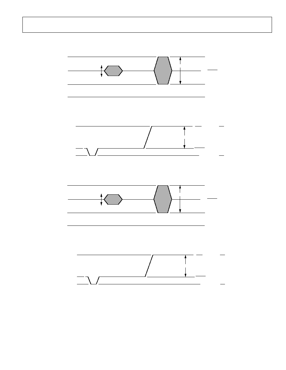
ADV7174/ADV7179
Rev. A | Page 47 of 52
PAL WAVEFORMS
650mV
317.7mV
989.7mV
0mV
PEAK CHROMA
BLANK/BLACK LEVEL
300mV (p-p)
672mV (p-p)
PEAK CHROMA
02980-A
-
068
Figure 69. PAL Composite Video Levels
1047mV
350.7mV
50.8mV
REF WHITE
SYNC LEVEL
BLANK/BLACK LEVEL
696.4mV
02980-A
-
069
Figure 70. PAL Luma Video Levels
650mV
317.7mV
989.7mV
0mV
PEAK CHROMA
BLANK/BLACK LEVEL
300mV (p-p)
672mV (p-p)
PEAK CHROMA
02980-A
-
070
Figure 71. PAL Chroma Video Levels
1050.2mV
351.8mV
51mV
REF WHITE
SYNC LEVEL
BLANK/BLACK LEVEL
698.4mV
02980-A
-
071
Figure 72. PAL RGB Video Levels

ADV7174/ADV7179
Rev. A | Page 48 of 52
Pb Pr WAVEFORMS
BETACAM LEVEL
0mV
+171mV
+334mV
+505mV
0mV
171mV
334mV
05mV
WHI
T
E
YELLOW
CY
AN
G
R
EEN
MA
GEN
T
A
RE
D
BLUE
BLACK
02980-A-072
Figure 73. NTSC 100% Color Bars, No Pedestal Pb Levels
BETACAM LEVEL
0mV
+158mV
+309mV
+467mV
0mV
158mV
309mV
467mV
WHITE
YELLO
W
CYAN
GREEN
MAGE
NT
A
RED
BL
UE
BL
ACK
02980-A-073
Figure 74. NTSC 100% Color Bars with Pedestal Pb Levels
SMPTE LEVEL
0mV
+118mV
+232mV
+350mV
0mV
118mV
232mV
350mV
WHITE
Y
E
LLOW
CYAN
G
R
EEN
MA
GE
N
T
A
RED
BLUE
BLACK
02980-A-074
Figure 75. PAL 100% Color Bars, Pb Levels
BETACAM LEVEL
0mV
+82mV
+423mV
+505mV
0mV
82mV
505mV
423mV
WHI
T
E
YELLOW
CY
AN
G
R
EEN
MA
GEN
T
A
RE
D
BLUE
BLACK
02980-A-075
Figure 76. NTSC 100% Color Bars, No Pedestal Pr Levels
BETACAM LEVEL
0mV
+76mV
+391mV
+467mV
0mV
76mV
467mV
391mV
WHI
T
E
YELLOW
CY
AN
G
R
EEN
MA
GEN
T
A
RE
D
BLUE
BLACK
02980-A-076
Figure 77. NTSC 100% Color Bars with Pedestal Pr Levels
SMPTE LEVEL
0mV
+57mV
+293mV
+350mV
0mV
57mV
350mV
293mV
WHI
T
E
Y
E
LLOW
CYAN
G
R
EEN
MAG
E
NT
A
RED
BLUE
BLACK
02980-A
-
077
Figure 78. PAL 100% Color Bars, Pr Levels
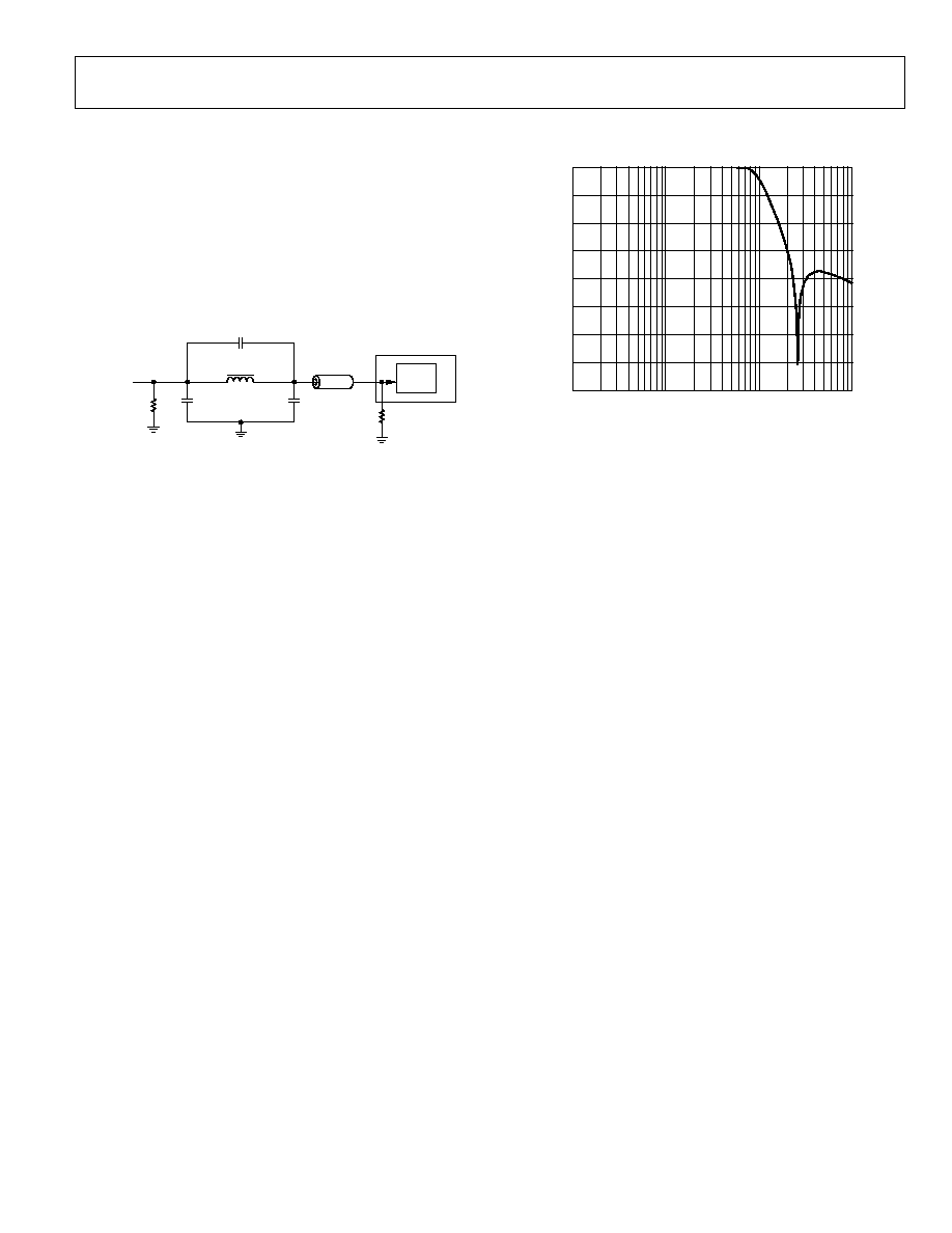
ADV7174/ADV7179
Rev. A | Page 49 of 52
APPENDIX 7--OPTIONAL OUTPUT FILTER
If an output filter is required for the CVBS, Y, UV, chroma, and
RGB outputs of the ADV7174/ADV7179, the filter shown in
Figure 79 can be used. Plots of the filter characteristics are
shown in Figure 80. An output filter is not required if the
outputs of the ADV7174/ADV7179 are connected to most
analog monitors or analog TVs. However, if the output signals
are applied to a system where sampling is used (e.g., digital
TVs), then a filter is required to prevent aliasing.
1.8
µ
H
75
270pF
22pF
DISPLAY DEVICE
Z
0
= 75
330pF
FILTER I/P
75
02980-
A-
078
Figure 79. Output Filter
FREQUENCY (Hz)
0
80
100k
MAGNITUDE
(dB)
70
60
50
40
30
20
10
1M
10M
100M
02980-A
-
079
Figure 80. Output Filter Plot

ADV7174/ADV7179
Rev. A | Page 50 of 52
APPENDIX 8--RECOMMENDED REGISTER VALUES
The ADV7174/ADV7179 registers can be set depending on the
user standard required. The power-on reset values can be found
in Figure 37.
The following examples give the various register formats for
several video standards. In each case, the output is set to compos-
ite output with all DACs powered up and with the input control
disabled. Additionally, the burst and BLANK color information
is enabled on the output, and the internal color bar generator is
switched off. In the examples shown, the timing mode is set to
Mode 0 in slave format. TR02TR00 of the Timing Register 0
control the timing modes. For a detailed explanation of each bit
in the command registers, refer to the Register Programming
section. TR07 should be toggled after setting up a new timing
mode. Timing Register 1 provides additional control over the
position and duration of the timing signals. In the examples,
this register is programmed in default mode.
Table 24. PAL B/D/G/H/I (F
SC
= 4.43361875 MHz)
Address
Description
Data
00H
Mode Register 0
05H
01H
Mode Register 1
10H
02H
Mode Register 2
00H
03H
Mode Register 3
00H
04H
Mode Register 4
00H
07H
Timing Register 0
00H
08H
Timing Register 1
00H
09H
Subcarrier Frequency Register 0
CBH
0AH
Subcarrier Frequency Register 1
8AH
0BH
Subcarrier Frequency Register 2
09H
0CH
Subcarrier Frequency Register 3
2AH
0DH
Subcarrier Phase Register
00H
0EH
Closed Captioning Ext Register 0
00H
0FH
Closed Captioning Ext Register 1
00H
10H
Closed Captioning Register 0
00H
11H
Closed Captioning Register 1
00H
12H
Pedestal Control Register 0
00H
13H
Pedestal Control Register 1
00H
14H
Pedestal Control Register 2
00H
15H
Pedestal Control Register 3
00H
16H
CGMS_WSS Register 0
00H
17H
CGMS_WSS Register 1
00H
18H
CGMS_WSS Register 2
00H
19H
Telext Request Control Register
00H
0FH
Closed Captioning Ext Register 1
00H
10H
Closed Captioning Register 0
00H
11H
Closed Captioning Register 1
00H
12H
Pedestal Control Register 0
00H
13H
Pedestal Control Register 1
00H
14H
Pedestal Control Register 2
00H
15H
Pedestal Control Register 3
00H
16H
CGMS_WSS Register 0
00H
17H
CGMS_WSS Register 1
00H
18H
CGMS_WSS Register 2
00H
19H
Teletext Request Control Register
00H
Table 25. PAL N (F
SC
= 4.43361875 MHz)
Address
Description
Data
00H
Mode Register 0
05H
01H
Mode Register 1
10H
02H
Mode Register 2
00H
03H
Mode Register 3
00H
04H
Mode Register 4
00H
07H
Timing Register 0
00H
08H
Timing Register 1
00H
09H
Subcarrier Frequency Register 0
CBH
0AH
Subcarrier Frequency Register 1
8AH
0BH
Subcarrier Frequency Register 2
09H
0CH
Subcarrier Frequency Register 3
2AH
0DH
Subcarrier Phase Register
00H
0EH
Closed Captioning Ext Register 0
00H
0FH
Closed Captioning Ext Register 1
00H
10H
Closed Captioning Register 0
00H
11H
Closed Captioning Register 1
00H
12H
Pedestal Control Register 0
00H
13H
Pedestal Control Register 1
00H
14H
Pedestal Control Register 2
00H
15H
Pedestal Control Register 3
00H
16H
CGMS_WSS Register 0
00H
17H
CGMS_WSS Register 1
00H
18H
CGMS_WSS Register 2
00H
19H
Teletext Request Control Register
00H

ADV7174/ADV7179
Rev. A | Page 51 of 52
Table 26. PAL-60 (F
SC
= 4.43361875 MHz)
Address Description
Data
00H
Mode Register 0
04H
01H
Mode Register 1
10H
02H
Mode Register 2
00H
03H
Mode Register 3
00H
04H
Mode Register 4
00H
07H
Timing Register 0
00H
08H
Timing Register 1
00H
09H
Subcarrier Frequency Register 0
CBH
0AH
Subcarrier Frequency Register 1
8AH
0BH
Subcarrier Frequency Register 2
09H
0CH
Subcarrier Frequency Register 3
2AH
0DH
Subcarrier Phase Register
00H
0EH
Closed Captioning Ext Register 0
00H
0FH
Closed Captioning Ext Register 1
00H
10H
Closed Captioning Register 0
00H
11H
Closed Captioning Register 1
00H
12H
Pedestal Control Register 0
00H
13H
Pedestal Control Register 1
00H
14H
Pedestal Control Register 2
00H
15H
Pedestal Control Register 3
00H
16H
CGMS_WSS Register 0
00H
17H
CGMS_WSS Register 1
00H
18H
CGMS_WSS Register 2
00H
19H
Teletext Request Control Register
00H
Table 27. NTSC (F
SC
= 3.5795454 MHz)
Address
Description
Data
00H
Mode Register 0
00H
01H
Mode Register 1
10H
02H
Mode Register 2
00H
03H
Mode Register 3
00H
04H
Mode Register 4
10H
07H
Timing Register 0
00H
08H
Timing Register 1
00H
09H
Subcarrier Frequency Register 0
1EH
1
0AH
Subcarrier Frequency Register 1
7CH
0BH
Subcarrier Frequency Register 2
F0H
0CH
Subcarrier Frequency Register 3
21H
0DH
Subcarrier Phase Register
00H
0EH
Closed Captioning Ext Register 0
00H
0FH
Closed Captioning Ext Register 1
00H
10H
Closed Captioning Register 0
00H
11H
Closed Captioning Register 1
00H
12H
Pedestal Control Register 0
00H
13H
Pedestal Control Register 1
00H
14H
Pedestal Control Register 2
00H
15H
Pedestal Control Register 3
00H
16H
CGMS_WSS Register 0
00H
17H
CGMS_WSS Register 1
00H
18H
CGMS_WSS Register 2
00H
19H
Teletext Request Control Register
00H
1
On power-up, this register is set to 16h. 1Eh should be written here for
correct F
SC
.
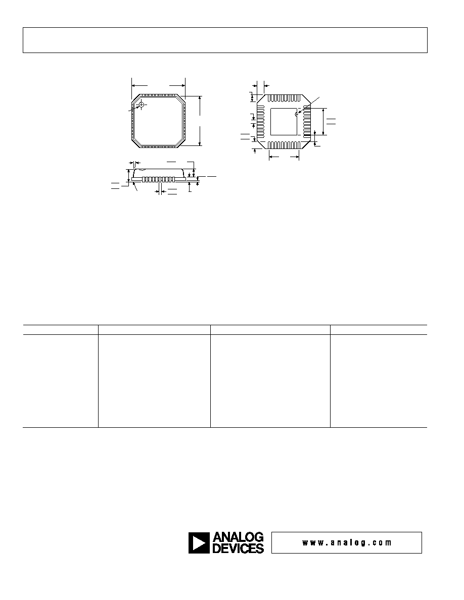
ADV7174/ADV7179
Rev. A | Page 52 of 52
OUTLINE DIMENSIONS
1
40
10
11
31
30
21
20
BOTTOM
VIEW
4.25
4.10 SQ
3.95
TOP
VIEW
6.00
BSC SQ
PIN 1
INDICATOR
5.75
BSC SQ
12° MAX
0.30
0.23
0.18
0.20 REF
SEATING
PLANE
1.00
0.85
0.80
0.05 MAX
0.02 NOM
COPLANARITY
0.08
0.80 MAX
0.65 TYP
4.50
REF
0.50
0.40
0.30
0.50
BSC
PIN 1
INDICATOR
0.60 MAX
0.60 MAX
0.25 MIN
COMPLIANT TO JEDEC STANDARDS MO-220-VJJD-2
Figure 81. 40-Lead Lead Frame Chip Scale Package [LFCSP]
(CP-40)
Dimensions shown in millimeters
Note that the exposed metal paddle on the bottom side of the LFCSP package must be soldered to PCB ground for proper heat dissipation
and also for noise and mechanical strength benefits.
ORDERING GUIDE
Model
Temperature Range
Package Description
Package Option
ADV7179KCP
0°C to 70°C
Lead Frame Chip Scale Package
CP-40
ADV7179KCP-REEL
0°C to 70°C
Lead Frame Chip Scale Package
CP-40
ADV7179BCP
-40°C to +85°C
Lead Frame Chip Scale Package
CP-40
ADV7179BCP-REEL
-40°C to +85°C
Lead Frame Chip Scale Package
CP-40
ADV7174KCP
0°C to 70°C
Lead Frame Chip Scale Package
CP-40
ADV7174KCP-REEL
0°C to 70°C
Lead Frame Chip Scale Package
CP-40
ADV7174BCP
-40°C to +85°C
Lead Frame Chip Scale Package
CP-40
ADV7174BCP-REEL
-40°C to +85°C
Lead Frame Chip Scale Package
CP-40
EVAL-ADV7179EBM
Evaluation
Board
EVAL-ADV7174EBM
Evaluation
Board
Purchase of licensed I
2
C components of Analog Devices or one of its sublicensed Associated Companies conveys a license for the purchaser under the Philips I
2
C Patent
Rights to use these components in an I
2
C system, provided that the system conforms to the I
2
C Standard Specification as defined by Philips.
© 2004 Analog Devices, Inc. All rights reserved. Trademarks and
registered trademarks are the property of their respective owners.
C0298002/04(A)
Document Outline