 | ÐлекÑÑоннÑй компоненÑ: ADV7175KS | СкаÑаÑÑ:  PDF PDF  ZIP ZIP |
Äîêóìåíòàöèÿ è îïèñàíèÿ www.docs.chipfind.ru
REV. A
Information furnished by Analog Devices is believed to be accurate and
reliable. However, no responsibility is assumed by Analog Devices for its
use, nor for any infringements of patents or other rights of third parties
which may result from its use. No license is granted by implication or
otherwise under any patent or patent rights of Analog Devices.
a
Integrated Digital CCIR-601
YCrCb to PAL/NTSC Video Encoder
ADV7175/ADV7176
© Analog Devices, Inc., 1996
One Technology Way, P.O. Box 9106, Norwood, MA 02062-9106, U.S.A.
Tel: 617/329-4700
Fax: 617/326-8703
FEATURES
CCIR-601 YCrCb to PAL/NTSC Video Encoder
Single 27 MHz Clock Required ( 2 Oversampling)
Pixel Port Supports:
CCIR-656 4:2:2 8-Bit Parallel Input Format
4:2:2 16-Bit Parallel Input Format
SMPTE 170M NTSC Compatible Composite Video Output
CCIR624/CCIR601 PAL Compatible Composite Video Output
SCART/PeriTV Support
YUV Output Mode
Simultaneous Composite and S-VHS Y/C or RGB YUV
Video Outputs
Programmable Luma Filters (Low-Pass/Notch)
Square Pixel Support (Slave Mode)
Allows Subcarrier Phase Locking with External Video
Source
10-Bit DAC Resolution for Encoded Video Channels
8-Bit DAC Resolution for RGB Output
YUV Interpolation for Accurate Subcarrier Construction
Programmable Subcarrier Frequency and Phase
Programmable LUMA Delay
Color Signal Control/Burst Signal Control
Interlaced/Noninterlaced Operation
Complete On-Chip Video Timing Generator
Master/Slave Operation Supported
Master Mode Timing Programmability
Macrovision Antitaping Facility Rev 6.1/7.x (ADV7175 Only)*
Close Captioning Support
Teletext Support (Passthrough Mode)
On-Board Color Bar Generation
On-Board Voltage Reference
2-Wire Serial MPU Interface (I
2
C Compatible)
+5 V CMOS Monolithic Construction
44-Pin PQFP Thermally Enhanced Package
APPLICATIONS
MPEG-1 and MPEG-2 Video
DVD
Digital Satellite/Cable Systems (Set Top Boxes/IRDs)
Video Games
CD Video/Karaoke
Professional Studio Quality
PC Video/Multimedia
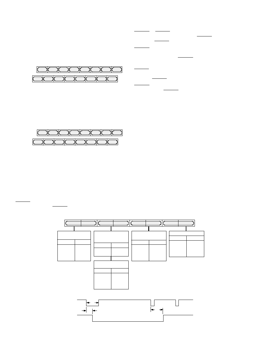
GENERAL DESCRIPTION
The ADV7175/ADV7176 is an integrated digital video encoder
that converts Digital CCIR-601 4:2:2 component video data into a
standard analog baseband television signal compatible with world
wide standards NTSC, PAL B/D/G/H/I, PAL M or PAL N. In
addition to the composite output signal, there is the facility to out-
put S-VHS Y/C video, YUV or RGB video. The Y/C, YUV or
RGB format is simultaneously available at the analog outputs with
the composite video signal. Each analog output generates a
standard video-level signal into a doubly terminated 75
load.
(Continued on page 6)
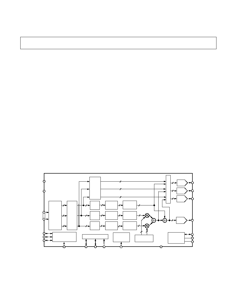
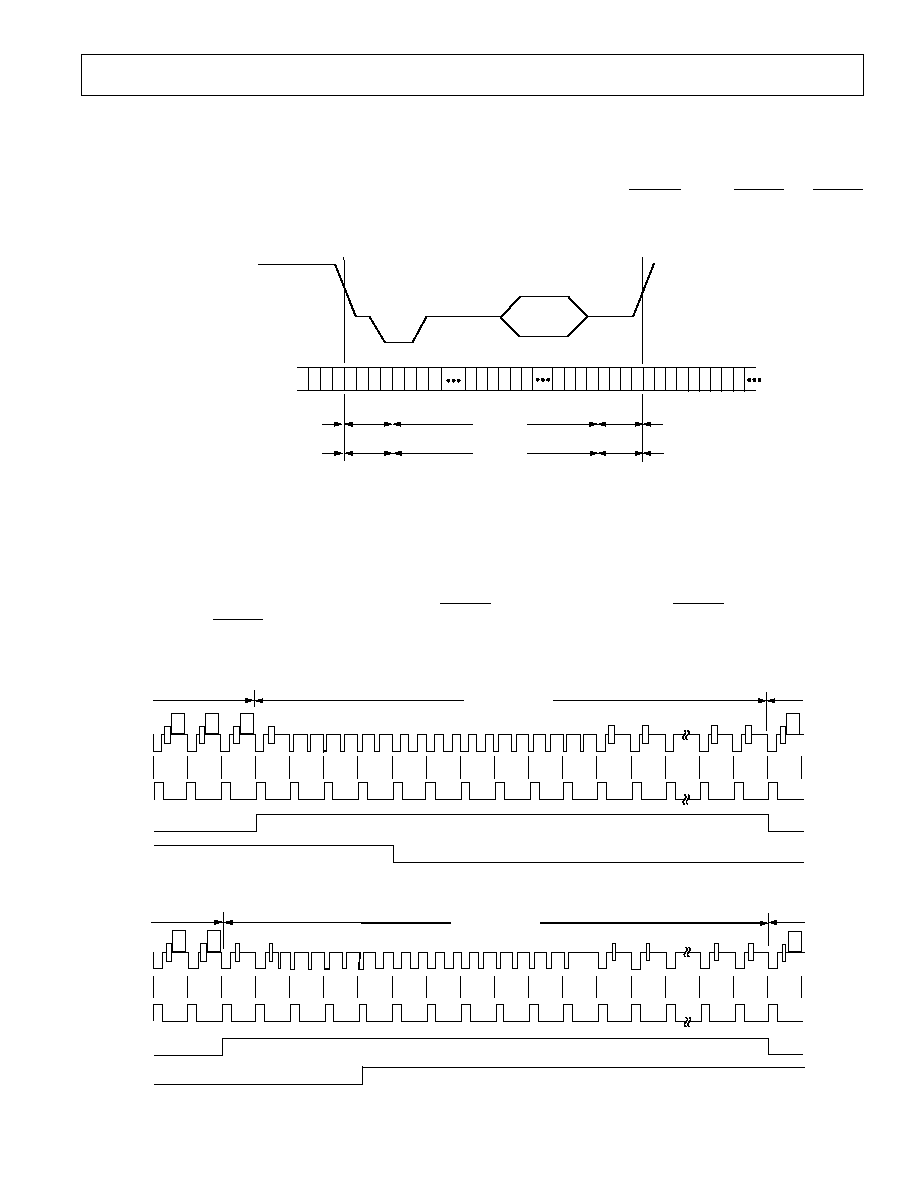
FUNCTIONAL BLOCK DIAGRAM
YUV TO
RBG
MATRIX
RESET
V
AA
8
8
8
10
8
8
8
10
8
8
8
10
INTER-
POLATOR
YCrCb
TO
YUV
MATRIX
SIN/COS
DDS BLOCK
10
10
8
10
10
10
10
M
U
L
T
I
P
L
E
X
E
R
VIDEO TIMING
GENERATOR
I
2
C MPU PORT
4:2:2 TO
4:4:4
INTER-
POLATOR
VOLTAGE
REFERENCE
CIRCUIT
SCLOCK SDATA ALSB
8
8
HSYNC
FIELD/
VSYNC
BLANK
CLOCK
GND
GREEN/
LUMA/
Y
RED/
CHROMA/
V
BLUE/
COMPOSITE/
U
COMPOSITE
V
REF
R
SET
COMP
V
LOW-PASS
FILTER
ADD
BURST
8
8
8
ADV7175/ADV7176
10-BIT
DAC
COLOR
DATA
P7P0
P15P8
10-BIT
DAC
10-BIT
DAC
REAL-TIME
CONTROL
CIRCUIT
SCRESET/RTC
INTER-
POLATOR
ADD
BURST
INTER-
POLATOR
ADD
SYNC
U
LOW-PASS
FILTER
Y
LOW-PASS
FILTER
10-BIT
DAC
*This device is protected by U.S. Patent Numbers 4631603, 4577216, 4819098 a nd other intellectual property rights. The Macrovision anticopy process is
licensed for noncommercial home use only, which is its sole intended use in the devic e. Please contact sales office for latest Macrovision version available.

ADV7175/ADV7176SPECIFICATIONS
REV. A
2
Model
ADV7175/ADV7176
Parameter
Conditions
1
Min
Typ
Max
Units
STATIC PERFORMANCE
Resolution (Each DAC)
10
Bits
Accuracy (Each DAC)
Integral Nonlinearity
±
1
LSB
Differential Nonlinearity
Guaranteed Monotonic
±
1
LSB
DIGITAL INPUTS
Input High Voltage, V
INH
2
V
Input Low Voltage, V
INL
0.8
V
Input Current, I
IN
V
IN
= 0.4 V or 2.4 V
±
1
µ
A
Input Capacitance, C
IN
10
pF
DIGITAL OUTPUTS
Output High Voltage, V
OH
I
SOURCE
= 400
µ
A
2.4
V
Output Low Voltage, V
OL
I
SINK
= 3.2 mA
0.4
V
Floating-State Leakage Current
10
µ
A
Floating-State Output Capacitance
10
pF
ANALOG OUTPUTS
Output Current
3
33
34.7
37
mA
Output Current
4
8
mA
Full-Scale DAC Output
182.5
IRE
LSB Size
33.9
µ
A
DAC-to-DAC Matching
2
5
%
Output Compliance, V
OC
0
+1.4
V
Output Impedance, R
OUT
15
k
Output Capacitance, C
OUT
I
OUT
= 0 mA
30
pF
VOLTAGE REFERENCE
Voltage Reference Range, V
REF
I
VREFOUT
= 20
µ
A
1.112
1.235
1.359
V
POWER REQUIREMENTS
5
V
AA
5
V
I
DAC
6
140
155
mA
I
CCT
7
110
150
mA
Power Supply Rejection Ratio
COMP = 0.1
µ
F
0.02
0.5
%/%
DYNAMIC PERFORMANCE
8
Luma Bandwidth
9
(Low-Pass Filter)
NTSC Mode
Stopband Cutoff
>50 dB Attenuation
7.5
MHz
Pass Band Cutoff
<0.06 dB Attenuation
2.3
MHz
Chroma Bandwidth
NTSC Mode
Stopband Cutoff
<40 dB Attenuation
3.6
MHz
Pass Band Cutoff
>0.1 dB Attenuation
1.0
MHz
Luma Bandwidth
9
(Low-Pass Filter)
PAL MODE
Stopband Cutoff
>50 dB Attenuation
8.0
MHz
Pass Band Cutoff
<0.06 dB Attenuation
3.4
MHz
Chroma Bandwidth
PAL MODE
Stopband Cutoff
<40 dB Attenuation
4.0
MHz
Pass Band Cutoff
>0.1 dB Attenuation
1.3
MHz
Differential Gain
0.8
%
Differential Phase
0.8
Degree
Differential Gain
Lower Power Mode
7
%
Differential Phase
Lower Power Mode
2
Degree
SNR
RMS
60
dB rms
SNR
Peak Periodic
56
dB p-p
Hue Accuracy
1.0
Degree
Color Saturation Accuracy
1.0
%
NOTES
1
±
5% for all versions.
2
Temperature range T
MIN
to T
MAX
: 0
°
C to 70
°
C.
3
Full
drive into 37.5
load.
4
Minimum drive with buffered/scaled output load.
5
Power measurements are taken with Clock Frequency = 27 MHz. Max T
J
= 100
°
C.
6
I
DAC
is the total current to drive all four DACs. Turning off one DAC reduces I
DAC
correspondingly.
7
I
CCT
(Circuit Currrent) is the continuous currrent required to drive the device.
8
Guaranteed by characterization.
9
These specifications are for the low-pass filter only. For the other internal filters please see Figure 3.
Specifications subject to change without notice.
(V
AA
= +5 V
1
, V
REF
= 1.235 V R
SET
= 150
. All specifications
T
MIN
to T
MAX
2
unless otherwise noted)

AC CHARACTERISTICS
1
Parameter
Min
Typ
Max
Units
Condition
Chroma Nonlinear Gain
0.6
±
%
Referenced to 40 IRE
Chroma Nonlinear Phase
1
±°
NTSC
Chroma Nonlinear Phase
1.7
±°
PAL
Chroma/Luma Intermod
0.2
±
%
Referenced to 714 mV (NTSC)
Chroma/Luma Intermod
0.4
±
%
Referenced to 700 mV (PAL)
Chroma/Luma Gain Ineq
0.6
±
%
Chroma/Luma Delay Ineq
1
ns
Luminance Nonlinearity
0.8
±
%
Chroma AM Noise
60
dB
Chroma PM Noise
59
dB
TIMINGSPECIFICATIONS
2
Parameter
Min
Typ
Max
Units
Condition
MPU PORT
1
SCLOCK Frequency
0
100
kHz
SCLOCK High Pulse Width, t
1
4.0
µ
s
SCLOCK Low Pulse Width, t
2
4.7
µ
s
Hold Time (Start Condition), t
3
4.0
µ
s
After this period the first clock pulse is generated
Setup Time (Start Condition), t
4
4.7
µ
s
Relevant for repeated start condition.
Data Setup Time, t
5
250
ns
SDATA, SCLOCK Rise Time, t
6
1
µ
s
SDATA, SCLOCK Fall Time, t
7
300
ns
Setup Time (Stop Condition), t
8
4.7
µ
s
ANALOG OUTPUTS
1, 5
Analog Output Delay
5
ns
DAC Analog Output Skew
0
ns
CLOCK CONTROL
AND PIXEL PORT
6
F
CLOCK
24.52 27
29.5
MHz
Clock High Time t
9
8
ns
Clock Low Time t
10
8
ns
Data Setup Time t
11
3.5
ns
Data Hold Time t
12
1
ns
Control Setup Time t
11
4
ns
Control Hold Time t
12
2
ns
Digital Output Access Time t
13
24
ns
Digital Output Hold Time t
14
6
ns
Pipeline Delay t
15
37
Clock Cycles
NOTES
1
Guaranteed by characterization.
2
TTL input values are 0 to 3 volts, with input rise/fall times
3 ns, measured between the 10% and 90% points. Timing reference points at 50% for inputs and
outputs. Analog Output Load
3 pF.
3
±
5% for all versions.
4
Temperature range (T
MIN
to T
MAX
); 0
°
C to +70
°
C.
5
Output delay measured from the 50% point of the rising edge of CLOCK to the 50% point of full-scale transition.
6
Pixel Port consists of the following inputs:
Pixel Inputs:
P15P0
Pixel Controls:
HSYNC,
FIELD/VSYNC, BLANK
Clock Input:
CLOCK
Specifications subject to change without notice.
ADV7175/ADV7176
REV. A
3
(V
AA
= +5 V
3
, V
REF
= 1.235 V R
SET
= 150
. All specifications T
MIN
to T
MAX
4
unless otherwise noted)
ADV7175/ADV7176
REV. A
4
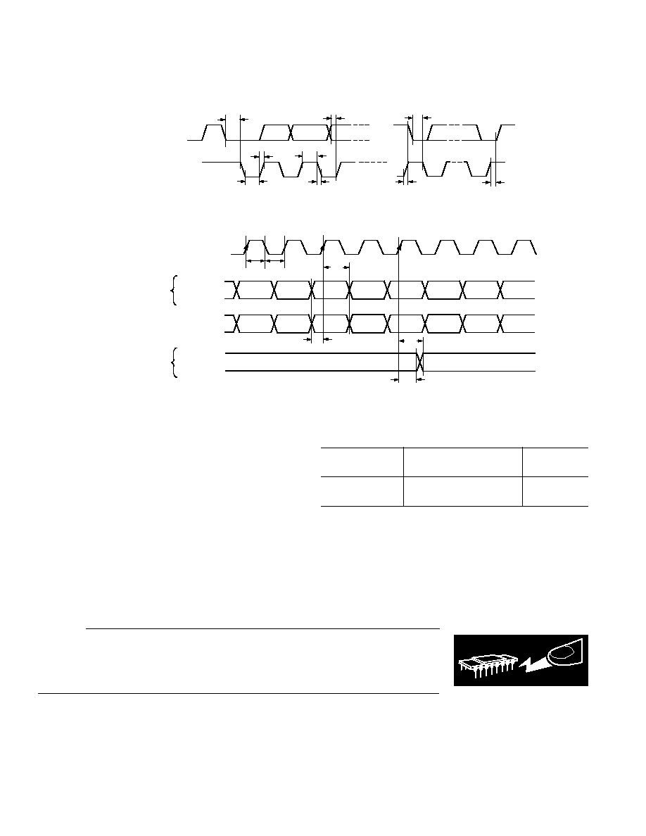
t
3
t
1
t
6
t
2
t
7
t
5
t
3
t
4
t
8
SDATA
SCLOCK
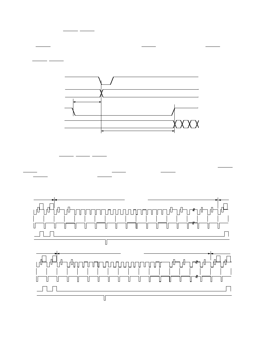
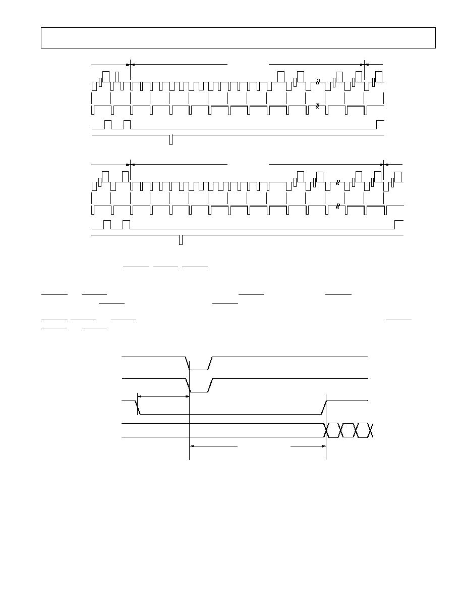
Figure 1. MPU Port Timing Diagram
t
9
t
11
CLOCK
PIXEL INPUT
DATA
t
10
t
12
HSYNC
,
FIELD/
VSYNC
,
BLANK
Cb
Y
Cr
Y
Cb
Y
HSYNC
,
FIELD/
VSYNC
,
BLANK
t
13
t
14
CONTROL
I/PS
CONTROL
O/PS
Figure 2. Pixel and Control Data Timing Diagram
ORDERING GUIDE
Temperature
Package
Model
Range
Option
ADV7175KS
0
°
C to +70
°
C
S-44
ADV7176KS
0
°
C to +70
°
C
S-44
ABSOLUTE MAXIMUM RATINGS
1
V
AA
to GND . . . . . . . . . . . . . . . . . . . . . . . . . . . . . . . . . . 7 V
Voltage on Any Digital Input Pin . GND 0.5 V to V
AA
+ 0.5 V
Storage Temperature (T
S
) . . . . . . . . . . . . . 65
°
C to +150
°
C
Junction Temperature (T
J
) . . . . . . . . . . . . . . . . . . . . +150
°
C
Lead Temperature (Soldering, 10 secs) . . . . . . . . . . . +260
°
C
Analog Outputs to GND
2
. . . . . . . . . . . . . GND 0.5 to V
AA
NOTES
1
Stresses above those listed under "Absolute Maximum Ratings" may cause
permanent damage to the device. This is a stress rating only and functional
operation of the device at these or any other conditions above those listed in the
operational sections of this specification is not implied. Exposure to absolute
maximum rating conditions for extended periods may affect device reliability.
2
Analog Output Short Circuit to any Power Supply or Common can be of an
indefinite duration.
WARNING!
ESD SENSITIVE DEVICE
CAUTION
ESD (electrostatic discharge) sensitive device. Electrostatic charges as high as 4000 V readily
accumulate on the human body and test equipment and can discharge without detection.
Although the ADV7175/ADV7176 feature proprietary ESD protection circuitry, permanent
damage may occur on devices subjected to high energy electrostatic discharges. Therefore,
proper ESD precautions are recommended to avoid performance degradation or loss of functionality.
ADV7175/ADV7176
REV. A
5
PIN DESCRIPTION
Mnemonic
Input/Output
Function
P15-P0
I
8-Bit 4:2:2 Multiplexed YCrCb Pixel Port (P7P0) or
16-Bit YCrCb Pixel Port (P15P0). P0 represents the LSB.
CLOCK
I
TTL Clock Input. Requires a stable 27 MHz reference Clock for proper operation.
Alternatively a 24.52 MHz (NTSC) or 29.5 MHz (PAL) can be used for square pixel
operation.
HSYNC
I/O
HSYNC
(Modes 1 & 2) Control Signal. This pin may be configured to output (Mas-
ter Mode) or accept (Slave Mode) Sync signals.
FIELD/VSYNC
I/O
Dual Function FIELD (Mode 1) and VSYNC (Mode 2) Control Signal. This pin may
be configured to output (Master Mode) or accept (Slave Mode) these control signals.
BLANK
I/O
Video Blanking Control Signal. The pixel inputs are ignored when this is logic level
"0." This signal is optional.
SCRESET/RTC
I
This pin can be configured as an input by setting MR22 and MR21 of Mode
Register 2. It can be configured as a subcarrier reset pin, in which case a high to low
transition on this pin will reset the subcarrier to field 0. Alternatively it may be con-
figured as a Real Time Control (RTC) input.
V
REF
I/O
Voltage Reference Input for DACs or Voltage Reference Output (1.2 V).
R
SET
I
A 150
resistor connected from this pin to GND is used to control full-scale ampli-
tudes of the video signals.
COMP
O
Compensation Pin. Connect a 0.1
µ
F capacitor from COMP to V
AA
.
COMPOSITE
O
PAL/NTSC Composite Video Output. Full-Scale Output is 180IRE (1286 mV) for
NTSC and 1300 mV for PAL.
RED/CHROMA/V
O
RED/S-VHS C/V Analog Output.
GREEN/LUMA/Y
O
GREEN/S-VHS Y/Y Analog Output.
BLUE/COMPOSITE/U
O
BLUE/Composite/U Analog Output.
SCLOCK
I
MPU Port Serial Interface Clock Input.
SDATA
I/O
MPU Port Serial Data Input/Output.
ALSB
I
TTL Address Input. This signal set up the LSB of the MPU address.
RESET
I
The input resets the on chip timing generator and sets the ADV7175/ADV7176 into
default mode. This is NTSC operation, Timing Slave Mode 0, 8-bit operation, 2
×
composite & S VHS out.
V
AA
P
+5 V Supply.
GND
G
Ground Pin.
PIN CONFIGURATION
12 13 14 15 16 17
18 19 20 21 22
3
4
5
6
7
1
2
10
11
8
9
40
39 38
41
42
43
44
36 35 34
37
29
30
31
32
27
28
25
26
23
24
33
PIN 1
IDENTIFIER
TOP VIEW
(Not to Scale)
V
REF
COMPOSITE
BLUE/COMPOSITE/U
V
AA
GND
V
AA
GREEN/LUMA/Y
BLANK
P13
P14
P15
HSYNC
FIELD/
VSYNC
ALSB
V
AA
P5
P6
P7
P8
P9
P10
P11
P12
GND
V
AA
RED/CHROMA/V
COMP
SDATA
SCLOCK
GND
V
AA
GND
RESET
CLOCK
GND
P4
P3
P2
P1
P0
V
AA
GND
SCRESET
/
RTC
R
SET
ADV7175/ADV7176
PQFP

ADV7175/ADV7176
REV. A
6
The ADV7175/ADV7176 is protected by U.S. Patent Numbers
5,343,196 and 5,442,355 and other intellectual property rights.
DATA PATH DESCRIPTION
For PAL B, D, G, H, I, M, N and NTSC M, N modes, YCrCb
4:2:2 data is input via the CCIR-656 compatible pixel port at a
13.5 MHz data rate. The pixel data is de-multiplexed to form
three data paths. Y has a range of 16 to 235, Cr and Cb have a
range of 128
±
112. The ADV7175/ADV7176 supports PAL
(B, D, G, H, I, N, M) and NTSC (with and without Pedestal)
standards. The appropriate SYNC, BLANK and burst levels are
added to the YCrCb data. Macrovision antitaping (ADV7175
only) and close-captioning levels are also added to Y and the
resultant data is interpolated to a rate of 27 MHz. The interpo-
lated data is filtered and scaled by three digital FIR filters.
The U and V signals are modulated by the appropriate subcarrier
sine/cosine phases and added together to make up the chromi-
nance signal. The luma (Y) signal can be delayed 1-3 luma
cycles (each cycle is 74 ns) with respect to the chroma signal.
The luma and chroma signals are then added together to make
up the composite video signal. All edges are slew rate limited.
The YCrCb data is also used to generate RGB data with appro-
priate SYNC and BLANK levels. The RGB data is in sychro-
nization with the composite video output. Alternatively analog
YUV data can be generated instead of RGB.
The four 10-bit DACs can be used to output:
1. 10-bit composite video + 8-bit RGB video.
2. 10-bit composite video + 8-bit YUV video.
3. Two 10-bit composite video signals
+ 10-bit LUMA & CHROMA (Y/C) signals.
Alternatively, each DAC can be individually powered off if not
required.
All possible video outputs are illustrated in Appendix 3, 4 and 5.
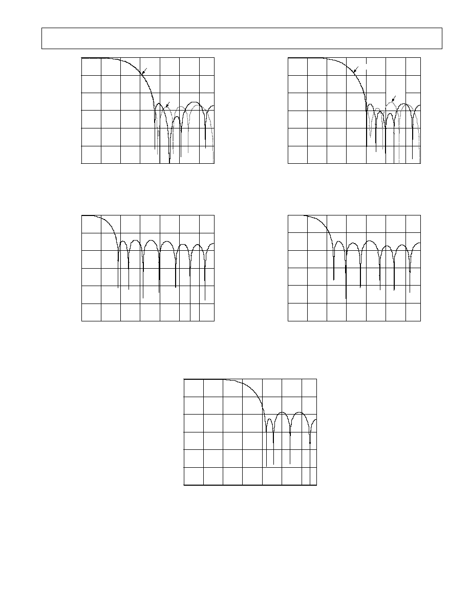
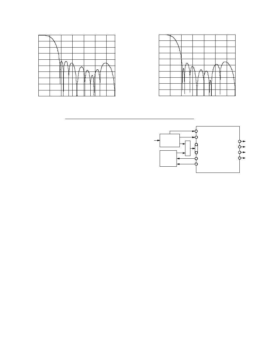
INTERNAL FILTER RESPONSE
The Y filter supports several different frequency responses in-
cluding two 4.5/5.0 MHz low-pass and PAL/NTSC subcarrier
notch responses. The U and V filters have a 0.6/1 0.3 MHz
low-pass response.
These filter characteristics are illustrated in Figures 3 to 11.
(Continued from page 1)
The ADV7175/ADV7176 also supports both a PAL and NTSC
square pixel mode in slave mode.
The video encoder accepts an 8-bit parallel pixel data stream in
CCIR-656 format or a 16-bit parallel data stream. This 4:2:2
data stream is interpolated into 4:4:4 component video (YUV).
The YUV video is interpolated to two times the pixel rate. The
color-difference components (UV) are quadrature modulated
using a subcarrier frequency generated by an on-chip synthesizer
(also running at two times the pixel rate). The two times pixel
rate sampling allows more accurate generation of the subcarrier
because frequency and phase errors are reduced by the higher
sampling rate. The ADV7175/ADV7176 also offers the option to
output the YUV information directly.
The luminance and chrominance components are digitally com-
bined and the resulting composite signal is output via a 10-bit
DAC. Three additional 10-/8-bit DACs are provided to output
S-VHS Y/C Video (10 bits), YUV or RGB Video (8 bits).
The output video frames are synchronized with the incoming
data timing reference codes. Optionally the encoder accepts (and
can generate) HSYNC, VSYNC & FIELD timing signals. These
timing signals can be adjusted to change pulse width and posi-
tion while the part is in the master mode. The encoder requires a
single two times pixel rate (27 MHz) clock for standard operation.
Alternatively the encoder requires 24.54 MHz clock for NTSC
or 29.5 MHz clock for PAL square pixel mode operation. All in-
ternal clocks are generated on-chip. The ADV7175/ADV7176
modes are set up over a two wire serial bidirectional port (I
2
C
Compatible) with two slave addresses.
Additionally, the ADV7175/ADV7176 allows a subcarrier phase
lock with an external video source and has a color bar generator
on-board.
Functionally the ADV7175 and ADV7176 are the same with
the exception that the ADV7175 can output the Macrovision
(Revision 6.1/7.x) anticopy algorithm.
The ADV7175/ADV7176 is fabricated in a +5 V CMOS pro-
cess. Its monolithic CMOS construction ensures greater func-
tionality with low power dissipation.
The ADV7175/ADV7176 is packaged in a 44-pin thermally en-
hanced PQFP package (patent pending).
MR04
MR03
NTSC
0
0
2.3
0.026
7.5
>
50
4.2
PAL
0
0
3.4
0.098
8.0
>
51.3
5.0
NTSC
0
1
1.0
0.085
3.57
>
27.6
2.1
PAL
0
1
1.4
0.107
4.43
>
29.3
2.7
NTSC/PAL
1 0
4.0
0.150
8.0
>
40
5.65
NTSC
1
1
2.3
0.054
7.5
>
54
4.2
PAL
1
1
3.4
0.106
8.0
>
50.3
5.0
FILTER SELECTION
F
3dB
PASSBAND
CUT OFF (MHz)
STOPBAND
CUT OFF (MHz)
PASSBAND
RIPPLE (dB)
STOPBAND
ATTENUATION (dB)
Figure 3. Y Filter Specifications
NTSC
1.0
0.085
3.6
>
40
0.3
2.05
PAL
1.3
0.04
4.0
>
40
0.02
2.45
FILTER SELECTION
F
3dB
PASSBAND
CUT OFF (MHz)
STOPBAND
CUT OFF (MHz)
PASSBAND
RIPPLE (dB)
STOPBAND
ATTENUATION (dB)
ATTENUATION @
1.3MHz (dB)
Figure 4. UV Filter Specifications
ADV7175/ADV7176
REV. A
7
FREQUENCY MHz
0
120
100
80
20
40
60
0
2
4
6
8
12
10
AMPLITUDE dB
TYPE A
TYPE B
Figure 5. NTSC Low-Pass Filter
FREQUENCY MHz
0
120
100
80
20
40
60
0
2
4
6
8
12
10
AMPLITUDE dB
Figure 6. NTSC Notch Filter
FREQUENCY MHz
0
120
100
80
20
40
60
0
2
4
6
8
12
10
AMPLITUDE dB
TYPE A
TYPE B
Figure 7. PAL Low-Pass Filter
FREQUENCY MHz
0
120
100
80
20
40
60
0
2
4
6
8
12
10
AMPLITUDE dB
Figure 8. PAL Notch Filter
FREQUENCY MHz
0
120
100
80
20
40
60
0
2
4
6
8
12
10
AMPLITUDE dB
Figure 9. NTSC/PAL Extended Mode Filter
ADV7175/ADV7176
REV. A
8
COLOR BAR GENERATION
The ADV7175/ADV7176 can be configured to generate 75%
amplitude, 75% saturation (75/7.5/75/7.5) for NTSC or 75%
amplitude, 100% saturation (100/0/75/0) for PAL color bars.
These are enabled by setting MR17 of Mode Register 1 to
Logic "1."
SQUARE PIXEL MODE
The ADV7175/ADV7176 can be used to operate in square
pixel mode. For NTSC operation an input clock of 24.54 MHz
is required. Alternatively, for PAL operation, an input clock of
29.5 MHz is required. The internal filters scale accordingly for
square pixel mode operation.
COLOR SIGNAL CONTROL
The color information can be switched on and off the video
output using Bit MR24 of Mode Register 2.
BURST SIGNAL CONTROL
The burst information can be switched on and off the video
output using Bit MR25 of Mode Register 2.
NTSC PEDESTAL CONTROL
The pedestal information on both odd and even fields can be
controlled on a line by line basis using the NTSC Pedestal
Control Registers. This allows the pedestals to be controlled
during the vertical blanking interval (Lines 10 to 25).
SUBCARRIER RESET
Together with the SCRESET/RTC PIN and Bits MR22 and
MR21 of Mode Register 2, the ADV7175/ADV7176 can be
used in subcarrier reset mode. The subcarrier will reset to field
0 at the start of the following field when a high to low transition
occurs on this input pin.
REAL TIME CONTROL
Together with the SCRESET/RTC PIN and Bits MR22 and
MR21 of Mode Register 2, the ADV7175/ADV7176 can be
used to lock an external video source. The real time control
mode allows the ADV7175/ADV7176 to automatically alter the
subcarrier frequency to compensate for line length variation.
When the part is connected to a device that outputs out a digi-
tal datastream in the RTC format (such as a Phillips SAA7110
video decoder), the part will automatically change to the com-
pensated subcarrier frequency on a line by line basis. This
digital datastream is 67 bits wide and the subcarrier is con-
tained in bits 0 to 21. Each bit is 2 clock cycles long.
COMPOSITE
VIDEO
e.g. VCR
OR CABLE
M
U
X
HSYNC
FIELD/
VSYNC
CLOCK
GREEN/LUMA/Y
RED/CHROMA/V
BLUE/COMPOSITE/U
COMPOSITE
ADV7175/ADV7176
P7P0
SCRESET/RTC
MPEG
DECODER
VIDEO
DECODER
(e.g.SAA7110)
Figure 12. RTC Connections
PIXEL TIMING DESCRIPTION
The ADV7175/ADV7176 can operate in either 8-bit or 16-bit
YCrCb Mode.
8-Bit YCrCb Mode
This default mode accepts multiplexed YCrCb inputs through
the P7P0 pixel inputs. The inputs follow the sequence Cb0,
Y0 Cr0, Y1 Cb1, Y2, etc. The Y, Cb and Cr data are input on
a rising clock edge.
16-Bit YCrCb Mode
This mode accepts Y inputs through the P7-P0 pixel inputs and
multiplexed CrCb inputs through the P15-P8 pixel inputs. The
data is loaded on every second rising clock edge of CLOCK.
The inputs follow the sequence Cb0, Y0 Cr0, Y1 Cb1, Y2, etc.
VIDEO TIMING DESCRIPTION
The ADV7175/ADV7176 is intended to interface to off the shelf
MPEG1 and MPEG2 Decoders. As a consequence the
ADV7175/ADV7176 accepts 4:2:2 YCrCb pixel data via a
CCIR-656 pixel port and has several video timing modes of
operation that allow it to be configured as either system master
video timing generator or a slave to the system video timing gen-
erator. The ADV7175/ADV7176 generates all of the required
horizontal and vertical timing periods and levels for the analog
video outputs.
The ADV7175/ADV7176 calculates the width and placement
of analog sync pulses, blanking levels and color burst envelopes.
Color bursts are disabled on appropriate lines and serration and
equalization pulses are inserted where required.
FREQUENCY MHz
0
2
4
6
8
12
10
AMPLITUDE dB
10
40
20
0
80
60
100
50
30
90
70
Figure 10. NTSC UV Filter
FREQUENCY MHz
0
2
4
6
8
12
10
AMPLITUDE dB
10
40
20
0
80
60
100
50
30
90
70
Figure 11. PAL UV Filter
(Continued on page 15)
ADV7175/ADV7176
REV. A
9
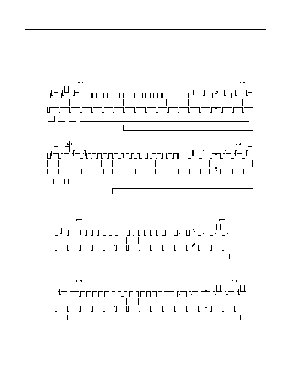
Mode 0 (CCIR-656): Slave Option.
(Timing Register 0 TR0 = X X X X X 0 0 0)
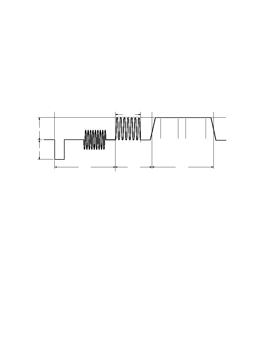
The ADV7175/ADV7176 is controlled by the SAV (Start Active Video) and EAV (End Active Video) time codes in the pixel data.
All timing information is transmitted using a 4-byte synchronization pattern. A synchronization pattern is sent immediately before
and after each line during active picture and retrace. Mode 0 is illustrated in Figure 13. The HSYNC, FIELD/VSYNC and BLANK
(if not used) pins should be tied high in this mode.
C
r
C
b
Y
F
F
0
0
0
0
X
Y
8
0
1
0
8
0
1
0
F
F
0
0
F
F
A
B
A
B
A
B
8
0
1
0
8
0
1
0
F
F
0
0
0
0
X
Y
C
b
Y C
r
C
b
Y C
r
C
b
Y C
r
EAV CODE
SAV CODE
ANCILLARY DATA
(HANC)
4 PIXELS
4 PIXELS
268 PIXELS
1440 PIXELS
4 PIXELS
4 PIXELS
280 PIXELS
1440 PIXELS
END OF ACTIVE
VIDEO LINE
START OF ACTIVE
VIDEO LINE
ANALOG
VIDEO
INPUT PIXELS
NTSC SYSTEM
PAL SYSTEM
Figure 13. Timing Mode 0 (Slave Mode)
Mode 0 (CCIR-656): Master Option.
(Timing Register 0 TR0 = X X X X X 0 0 1)
The ADV7175/ADV7176 generates H, V and F signals required for the SAV (start active video) and EAV (end active video) time
codes in the CCIR656 standard. The H bit is output on the HSYNC pin, the V bit is output on the BLANK pin and the F bit is
output on the FIELD/VSYNC pin. Mode 0 is illustrated in Figure 14 (NTSC) and Figure 15 (PAL). The H, V and F transitions
relative to the video waveform are illustrated in Figure 16.
522
523
524
525
1
2
3
4
5
6
7
8
9
10
11
20
21
22
DISPLAY
DISPLAY
VERTICAL BLANK
ODD FIELD
EVEN FIELD
H
V
F
260
261
262
263
264
265
266
267
268
269
270
271
272
273
274
283
284
285
ODD FIELD
EVEN FIELD
DISPLAY
DISPLAY
VERTICAL BLANK
H
V
F
Figure 14. Timing Mode 0 (NTSC Master Mode)
ADV7175/ADV7176
REV. A
10
622
623
624
625
1
2
3
4
5
6
7
21
22
23
DISPLAY
DISPLAY
VERTICAL BLANK
H
V
F
ODD FIELD
EVEN FIELD
309
310
311
312
314
315
316
317
318
319
320
334
335
336
DISPLAY
DISPLAY
VERTICAL BLANK
H
V
F
ODD FIELD
EVEN FIELD
313
Figure 15. Timing Mode 0 (PAL Master Mode)
ANALOG
VIDEO
H
F
V
Figure 16. Timing Mode 0 Data Transitions (Master Mode)
ADV7175/ADV7176
REV. A
11
Mode 1: Slave Option. HSYNC, BLANK, FIELD.
(Timing Register 0 TR0 = X X X X X 0 1 0)
In this mode the ADV7175/ADV7176 accepts horizontal SYNC and Odd/Even FIELD signals. A transition of the FIELD input
when HSYNC is low indicates a new frame, i.e., vertical retrace. The BLANK signal is optional. When the BLANK input is disabled
the ADV7175/ADV7176 automatically blanks all normally blank lines as per CCIR-624. Mode 1 is illustrated in Figure 17 (NTSC)
and Figure 18 (PAL).
260
261
262
263
264
265
266
267
268
269
270
271
272
273
274
283
284
285
ODD FIELD
EVEN FIELD
DISPLAY
DISPLAY
VERTICAL BLANK
HSYNC
BLANK
FIELD
522
523
524
525
1
2
3
4
5
6
7
8
9
10
11
20
21
22
DISPLAY
DISPLAY
VERTICAL BLANK
ODD FIELD
EVEN FIELD
HSYNC
BLANK
FIELD
Figure 17. Timing Mode 1 (NTSC)
622
623
624
625
1
2
3
4
5
6
7
21
22
23
DISPLAY
VERTICAL BLANK
ODD FIELD
EVEN FIELD
HSYNC
BLANK
FIELD
DISPLAY
309
310
311
312
313
314
315
316
317
318
319
334
335
336
DISPLAY
VERTICAL BLANK
ODD FIELD
EVEN FIELD
HSYNC
BLANK
FIELD
DISPLAY
320
Figure 18. Timing Mode 1 (PAL)
ADV7175/ADV7176
REV. A
12
Mode 1: Master Option. HSYNC, BLANK, FIELD.
(Timing Register 0 TR0 = X X X X X 0 1 1)
In this mode the ADV7175/ADV7176 can generate horizontal SYNC and Odd/Even FIELD signals. A transition of the FIELD
input when HSYNC is low indicates a new frame i.e., vertical retrace. The BLANK signal is optional. When the BLANK input is
disabled the ADV7175/ADV7176 automatically blanks all normally blank lines as per CCIR-624. Pixel data is latched on the rising
clock edge following the timing signal transitions. Mode 1 is illustrated in Figure 17 (NTSC) and Figure 18 (PAL). Figure 19 illus-
trates the HSYNC, BLANK and FIELD for an odd or even field transition relative to the pixel data.
HSYNC
FIELD
BLANK
PIXEL
DATA
PAL = 12 * CLOCK/2
NTSC = 16 * CLOCK/2
PAL = 132 * CLOCK/2
NTSC = 118 * CLOCK/2
Cb
Y
Cr
Y
Figure 19. Timing Mode 1 Odd/Even Field Transitions
Mode 2: Slave Option. HSYNC, VSYNC, BLANK.
(Timing Register 0 TR0 = X X X X X 1 0 0)
In this mode the ADV7175/ADV7176 accepts horizontal and vertical SYNC signals. A coincident low transition of both HSYNC
and VSYNC inputs indicates the start of an odd field. A VSYNC low transition when HSYNC is high indicates the start of an even
field. The BLANK signal is optional. When the BLANK input is disabled, the ADV7175/ADV7176 automatically blanks all nor-
mally blank lines as per CCIR-624. Mode 2 is illustrated in Figure 20 (NTSC) and Figure 21 (PAL).
522
523
524
525
1
2
3
4
5
6
7
8
9
10
11
20
21
22
DISPLAY
DISPLAY
VERTICAL BLANK
ODD FIELD
EVEN FIELD
HSYNC
BLANK
VSYNC
260
261
262
263
264
265
266
267
268
269
270
271
272
273
274
283
284
285
ODD FIELD
EVEN FIELD
DISPLAY
DISPLAY
VERTICAL BLANK
HSYNC
BLANK
VSYNC
Figure 20. Timing Mode 2 (NTSC)
ADV7175/ADV7176
REV. A
13
622
623
624
625
1
2
3
4
5
6
7
21
22
23
DISPLAY
VERTICAL BLANK
ODD FIELD
EVEN FIELD
HSYNC
BLANK
VSYNC
DISPLAY
309
310
311
312
313
314
315
316
317
318
319
334
335
336
DISPLAY
VERTICAL BLANK
ODD FIELD
EVEN FIELD
HSYNC
BLANK
DISPLAY
320
VSYNC
Figure 21. Timing Mode 2 (PAL)
Mode 2: Master Option. HSYNC, VSYNC, BLANK.
(Timing Register 0 TR0 = X X X X X 1 0 1 )
In this mode the ADV7175/ADV7176 can generate horizontal and vertical SYNC signals. A coincident low transition of both
HSYNC
and VSYNC inputs indicates the start of an odd field. A VSYNC low transition when HSYNC is high indicates the start of
an even field. The BLANK signal is optional. When the BLANK input is disabled the ADV7175/ADV7176 automatically blanks all
normally blank lines as per CCIR-624. Mode 2 is illustrated in Figure 20 (NTSC) and Figure 21 (PAL). Figure 22 illustrates the
HSYNC
, BLANK and VSYNC for an even to odd field transition relative to the pixel data. Figure 23 illustrates the HSYNC,
BLANK
and VSYNC for an odd to even field transition relative to the pixel data.
PAL = 12* CLOCK/2
NTSC = 16 * CLOCK/2
LINE 3
LINE 4
HSYNC
VSYNC
BLANK
PIXEL
DATA
PAL = 132* CLOCK/2
NTSC = 118 * CLOCK/2
Cb
Y
Cr
Y
Figure 22. Timing Mode 2 Even-to-Odd Field Transition
ADV7175/ADV7176
REV. A
14
PAL = 864 * CLOCK/2
NTSC = 858 * CLOCK/2
PAL = 132 * CLOCK/2
NTSC = 118 * CLOCK/2
LINE 265
LINE 266
HSYNC
VSYNC
BLANK
PIXEL
DATA
PAL = 12 * CLOCK/2
NTSC = 16 * CLOCK/2
Cb
Y
Cr
Y
Cb
Figure 23. Timing Mode 2 Odd-to-Even Field Transition
Mode 3: Master/Slave Option. HSYNC, BLANK, FIELD.
(Timing Register 0 TR0 = X X X X X 1 1 0 or X X X X X 1 1 1)
In this mode the ADV7175/ADV7176 accepts or generates Horizontal SYNC and odd/even FIELD signals. A transition of the
FIELD input when HSYNC is high indicates a new frame i.e., vertical retrace. The BLANK signal is optional. When the BLANK
input is disabled the ADV7175/ADV7176 automatically blanks all normally blank lines as per CCIR-624. Mode 3 is illustrated in
Figure 24 (NTSC) and Figure 25 (PAL).
260
261
262
263
264
265
266
267
268
269
270
271
272
273
274
283
284
285
ODD FIELD
EVEN FIELD
DISPLAY
DISPLAY
VERTICAL BLANK
HSYNC
BLANK
FIELD
522
523
524
525
1
2
3
4
5
6
7
8
9
10
11
20
21
22
DISPLAY
DISPLAY
VERTICAL BLANK
ODD FIELD
EVEN FIELD
HSYNC
BLANK
FIELD
Figure 24. Timing Mode 3 (NTSC)
ADV7175/ADV7176
REV. A
15
622
623
624
625
1
2
3
4
5
6
7
21
22
23
DISPLAY
VERTICAL BLANK
ODD FIELD
EVEN FIELD
HSYNC
BLANK
FIELD
DISPLAY
309
310
311
312
313
314
315
316
317
318
319
334
335
336
DISPLAY
VERTICAL BLANK
ODD FIELD
EVEN FIELD
HSYNC
BLANK
FIELD
DISPLAY
320
Figure 25. Timing Mode 3 (PAL)
PALInterlaced: Scan lines 16, 311318 and 624625 are al-
ways blanked and vertical sync pulses are included in Fields 1,
2, 5 and 6. Scan lines 15, 311319 and 624625 are always
blanked and vertical sync pulses are included in Fields 3, 4, 7
and 8. The remaining scan lines in the vertical interval are also
blanked and can be used for close captioning data. Burst is dis-
abled on lines 16, 311318 and 623625 in Fields 1, 2, 5 and
6. Burst is disabled on lines 15, 311319 and 623625 in
Fields 3, 4, 7 and 8.
PALNoninterlaced: Scan lines 16 and 311312 are always
blanked and vertical sync pulses are included. The remaining
scan lines in the vertical interval are also blanked and can be
used for close captioning data. Burst is disabled on lines 15,
310312.
POWER-ON RESET
After power-up, it is necessary to execute a reset operation. A
reset occurs on the falling edge of a high to low transition on the
RESET
pin. This initializes the pixel port such that the pixel
inputs P7P0 are selected. After reset, the ADV7175/ADV7176
is automatically set up to operate in NTSC mode. Subcarrier
frequency code 21F07C16 HEX is loaded into the subcarrier
frequency registers. All other registers, with the exception of
Mode Register 0, are set to 00H. All bits in Mode Register 0
are set to Logic Level "0" except Bit MR02. Bit MR02 of
Mode Register 0 is set to Logic "1." This enables the 7.5 IRE
pedestal.
In addition the ADV7175/ADV7176 supports a PAL or NTSC
square pixel operation in slave mode. The part requires an in-
put pixel clock of 24.54 MHz for NTSC and an input pixel
clock of 29.5 MHz for PAL. The internal horizontal line
counters place the various video waveform sections in the cor-
rect location for the new clock frequencies.
The ADV7175/ADV7176 has 8 distinct master or slave timing
configurations. These are divided into 4 timing modes which
operate at one discrete clock frequency (27 MHz). Timing con-
trol is established with the bidirectional SYNC, BLANK and
FIELD/VSYNC pins. Timing Mode Register 1 can also be
used to vary the timing pulse widths and the where they occur in
relation to each other.
OUTPUT VIDEO TIMING
The video timing generator generates the appropriate SYNC,
BLANK and BURST sequence that controls the output analog
waveforms. These sequences are summarized below. In slave
modes the following sequences are synchronized with the input
timing control signals. In master modes the timing generator
free runs and generates the following sequences in addition to
the output timing control signals.
NTSCInterlaced: Scan lines 19 and 264272 are always
blanked and vertical sync pulses are included. Scan lines 525,
1021 and 262, 263, 273284 are also blanked and can be used
for close captioning data. Burst is disabled on lines 16, 261
269 and 523525.
NTSCNoninterlaced: Scan lines 19 are always blanked
and vertical sync pulses are included. Scan lines 1021 are also
blanked and can be used for close captioning data. Burst is dis-
abled on lines 16, 261262.
(Continued from page 8)
ADV7175/ADV7176
REV. A
16
MPU PORT DESCRIPTION
The ADV7175 and ADV7176 support a two wire serial (I
2
C
compatible) microprocessor bus driving multiple peripherals.
Two inputs serial data (SDATA) and serial clock (SCLOCK)
carry information between any device connected to the bus.
Each slave device is recognized by a unique address. The
ADV7175 and ADV7176 each have four possible slave ad-
dresses for both read and write operations. These are unique
addresses for each device and are illustrated in Figure 26 and
Figure 27. The LSB sets either a read or write operation.
Logic Level "1" corresponds to a read operation while Logic
Level "0" corresponds to a write operation. A1 is set by setting
the ALSB pin of the ADV7175/ADV7176 to Logic Level "0" or
Logic Level "1."
1
X
1
0
1
0
1
A1
ADDRESS
CONTROL
SET UP BY
ALSB
READ/WRITE
CONTROL
0
WRITE
1
READ
Fig 26. ADV7175 Slave Address
0
X
1
0
1
0
1
A1
ADDRESS
CONTROL
SET UP BY
ALSB
READ/WRITE
CONTROL
0
WRITE
1
READ
Fig 27. ADV7176 Slave Address
To control the various devices on the bus the following protocol
must be followed. First the master initiates a data transfer by es-
tablishing a start condition, defined by a high to low transition
on SDATA while SCLOCK remains high. This indicates that
an address/data stream will follow. All peripherals respond to
the start condition and shift the next eight bits (7-bit address +
R/W bit). The bits transferred from MSB down to LSB. The
peripheral that recognizes the transmitted address responds by
pulling the data line low during the ninth clock pulse. This is
known as an acknowledge bit. All other devices withdraw from
the bus at this point and maintain an idle condition. The idle
condition is where the device monitors the SDATA and SCLOCK
lines waiting for the Start condition and the correct transmitted
address. The R/W bit determines the direction of the data. A
Logic "0" on the LSB of the first byte means that the master
will write information to the peripheral. A Logic "1" on the
LSB of the first byte means that the master will read informa-
tion from the peripheral.
The ADV7175/ADV7176 acts as a standard slave device on the
bus. The data on the SDATA pin is 8 bits long supporting the
7-bit addresses plus the R/W bit. The ADV7175 has 33 sub-
addresses and the ADV7176 has 19 subaddresses to enable ac-
cess to the internal registers. It, therefore, interprets the first
byte as the device address and the second byte as the starting
subaddress. The subaddresses auto increment allowing data to
be written to or from the starting subaddress. A data transfer is
always terminated by a stop condition. The user can also access
any unique subaddress register on a one by one basis without
having to update all the registers. There is one exception. The
Subcarrier Frequency Registers should be updated in sequence,
starting with Subcarrier Frequency Register 0. The auto incre-
ment function should be then used to increment and access
subcarrier frequency registers 1, 2 and 3. The subcarrier fre-
quency registers should not be accessed independently.
Stop and start conditions can be detected at any stage during
the data transfer. If these conditions are asserted out of se-
quence with normal read and write operations, then these cause
an immediate jump to the idle condition. During a given
SCLOCK high period the user should only issue one start con-
dition, one stop condition or a single stop condition followed by
a single start condition. If an invalid subaddress is issued by the
user, the ADV7175/ADV7176 will not issue an acknowledge
and will return to the idle condition. If in auto-increment
mode, the user exceeds the highest subaddress then the follow-
ing action will be taken:
1. In Read Mode the highest subaddress register contents will
continue to be output until the master device issues a no-ac-
knowledge. This indicates the end of a read. A no-acknowledge
condition is where the SDATA line is not pulled low on the
ninth pulse.
2. In Write Mode, the data for the invalid byte will be not be
loaded into any subaddress register, a no-acknowledge will
be issued by the ADV7175/ADV7176 and the part will re-
turn to the idle condition.
Figure 28 illustrates an example of data transfer for a read se-
quence and the start and stop conditions.
1-7
8
9
1-7
8
9
1-7
8
9
P
S
START ADDR R/
W
ACK SUBADDRESS ACK
DATA
ACK
STOP
SDATA
SCLOCK
Figure 28. Bus Data Transfer
Figure 29 shows bus write and read sequences.
DATA
A(S)
S
SLAVE ADDR
A(S)
SUB ADDR
A(S)
LSB = 0
LSB = 1
DATA
A(S)
P
S
SLAVE ADDR
A(S)
SUB ADDR
A(S) S
SLAVE ADDR
A(S)
DATA
A(M)
A
(M)
DATA
P
WRITE
SEQUENCE
READ
SEQUENCE
A
(S) = NO-ACKNOWLEDGE BY SLAVE
A
(M) = NO-ACKNOWLEDGE BY MASTER
A(S) = ACKNOWLEDGE BY SLAVE
A(M) = ACKNOWLEDGE BY MASTER
S = START BIT
P = STOP BIT
Figure 29. Write and Read Sequences
ADV7175/ADV7176
REV. A
17
SR4
SR3
SR2
SR1
SR0
SR7
SR6
SR5
SR4
SR3 SR2 SR1 SR0
ZERO SHOULD
BE WRITTEN TO
THESE BITS
SR7SR5
(000)
SUBADDRESS REGISTER
0 0 0 0 0 MODE REGISTER 0
0 0 0 0 1 MODE REGISTER 1
0 0 0 1 0 SUB CARRIER FREQ REGISTER 0
0 0 0 1 1 SUB CARRIER FREQ REGISTER 1
0 0 1 0 0 SUB CARRIER FREQ REGISTER 2
0 0 1 0 1 SUB CARRIER FREQ REGISTER 3
0 0 1 1 0 SUB CARRIER PHASE REGISTER
0 0 1 1 1 TIMING MODE REGISTER 0
0 1 0 0 0 CLOSED CAPTIONING EXTENDED DATA BYTE 0
0 1 0 0 1 CLOSED CAPTIONING EXTENDED DATA BYTE 1
0 1 0 1 0 CLOSED CAPTIONING DATA BYTE 0
0 1 0 1 1 CLOSED CAPTIONING DATA BYTE 1
0 1 1 0 0 TIMING MODE REGISTER 1
0 1 1 0 1 MODE REGISTER 2
0 1 1 1 0 NTSC PEDESTAL CONTROL REG 0 (FIELD 1/3)
0 1 1 1 1 NTSC PEDESTAL CONTROL REG 1 (FIELD 1/3)
1 0 0 0 0 NTSC PEDESTAL CONTROL REG 2 (FIELD 2/4)
1 0 0 0 1 NTSC PEDESTAL CONTROL REG 3 (FIELD 2/4)
1 0 0 1 0 MODE REGISTER 3
1 0 0 1 1 MACROVISION REGISTERS (ADV7175 ONLY)
· · · · · "
"
"
· · · · · "
"
"
1 1 1 1 1 MACROVISION REGISTERS (ADV7175 ONLY)
Figure 30. Subaddress Register
REGISTER ACCESSES
The MPU can write to or read from all of the registers of the
ADV7175/ADV7176 except the subaddress register which is a
write only register. The subaddress register determines which
register the next read or write operation accesses. All communi-
cations with the part through the bus start with an access to the
subaddress register. Then a read/write operation is performed
from/to the target address which then increments to the next
address until a stop command on the bus is performed.
REGISTER PROGRAMMING
The following section describes each register, including
subaddress register, mode registers, subcarrier frequency regis-
ters, subcarrier phase register, timing registers, closed captioning
extended data registers, closed captioning data registers and
NTSC pedestal control registers in terms of its configuration.
Subaddress Register (SR7SR0)
The communications register is an eight bit write-only register.
After the part has been accessed over the bus and a read/write
operation is selected, the subaddress set up. The subaddress
register determines to/from which register the operation takes
place.
Figure 30 shows the various operations under the control of the
subaddress register. Zero should always be written to SR7
SR5.
Register Select (SR4SR0):
These bits are setup to point to the required starting address.
MODE REGISTER 0 MR0 (MR07MR00)
(Address (SR4SR0) = 00H)
Mode Register 0 is a 8-bit wide register.
Figure 31 shows the various operations under the control of
Mode Register 0. This register can be read from as well written to.
MR01
MR00
MR07
MR02
MR04
MR03
MR05
MR06
OUTPUT VIDEO
STANDARD SELECTION
0
0
NTSC
0
1
PAL (B, D, G, H, I)
1
0
PAL (M)
1
1
RESERVED
MR01 MR00
MR07
(0)
ZERO SHOULD
BE WRITTEN TO
THIS BIT
OUTPUT SELECT
0
YC OUTPUT
1
RGB/YUV OUTPUT
MR06
FILTER SELECT
0
0
LOW PASS FILTER (A)
0
1
NOTCH FILTER
1
0
EXTENDED MODE
1
1
LOW PASS FILTER (B)
MR04 MR03
RGB SYNC
0
DISABLE
1
ENABLE
MR05
PEDESTAL CONTROL
0
PEDESTAL OFF
1
PEDESTAL ON
MR02
Figure 31. Mode Register 0
ADV7175/ADV7176
REV. A
18
MODE REGISTER 1 MR1 (MR17MR10)
(Address (SR4SR0) = 01H)
Mode Register 1 is a 8-bit wide register.
Figure 32 shows the various operations under the control of Mode
Register 1. This register can be read from as well written to.
MODE REGISTER 1 (MR17MR10) BIT DESCRIPTION
Interlaced Mode Control (MR10):
This bit is used to setup the output to interlaced or non-inter-
laced mode. This mode is only relevant when the part is in
composite video mode.
Closed Captioning Field Control (MR12MR11)
These bits control the field that close captioning data is displayed
on close captioning information can be displayed on an odd field,
even field or both fields.
DAC Control (MR16MR13)
These bits can be used to power down the DACs. This can be
used to reduce the power consumption of the ADV7175/ADV7176
if any of the DACs are not required in the application.
Color Bar Control (MR17)
This bit can be used to generate and output an internal color
bar. The color bar configuration is 75/75/75/7.5 for NTSC and
100/0/75/0 for PAL.
MR11
MR10
MR17
MR12
MR13
MR15
MR16
MR14
CLOSED CAPTIONING
FIELD SELECTION
0
0
NO DATA OUT
0
1
ODD FIELD ONLY
1
0
EVEN FIELD ONLY
1
1
DATA OUT
(BOTH FIELDS)
MR12 MR11
COMPOSITE DAC
CONTROL
0
NORMAL
1
POWER DOWN
MR16
GREEN/LUMA
DAC CONTROL
0
NORMAL
1
POWER DOWN
MR14
RED/CHROMA
DAC CONTROL
0
NORMAL
1
POWER DOWN
MR13
BLUE/COMPOSITE
DAC CONTROL
0
NORMAL
1
POWER DOWN
MR15
INTERLACE
CONTROL
0
INTERLACED
1
NON-INTERLACED
MR10
COLOR BAR
CONTROL
0
DISABLE
1
ENABLE
MR17
Figure 32. Mode Register 1
MODE REGISTER 0 (MR07MR00) BIT DESCRIPTION
Encode Mode Control (MR01MR00):
These bits are used to set up the encode mode. The ADV7175/
ADV7176 can be set up to output NTSC, PAL (B, D, G, H, I),
PAL (M) and PAL (N) standard video.
Pedestal Control (MR02)
This bit specifies whether a pedestal is to be generated on the
NTSC composite video signal. This bit is invalid if the
ADV7175/ADV7176 is configured in PAL mode.
Luminance Filter Control (MR04MR03)
These bits are used for selecting between a filter for the lumi-
nance signal. These filters automatically are set to the cutoff fre-
quency for the low-pass filters and the subcarrier frequency for
the notch filter. The extended mode filter is a 5.5 MHz low-pass
filter. The filters are illustrated in Figures 3 to 11.
RGB Sync (MR05)
This bit is used to set up the RGB outputs with the sync infor-
mation encoded.
Output Control (MR06)
This bit specifies if the part is in composite video or RGB/YUV
mode. Please note that in RGB/YUV mode the main composite
signal is still available.
ADV7175/ADV7176
REV. A
19
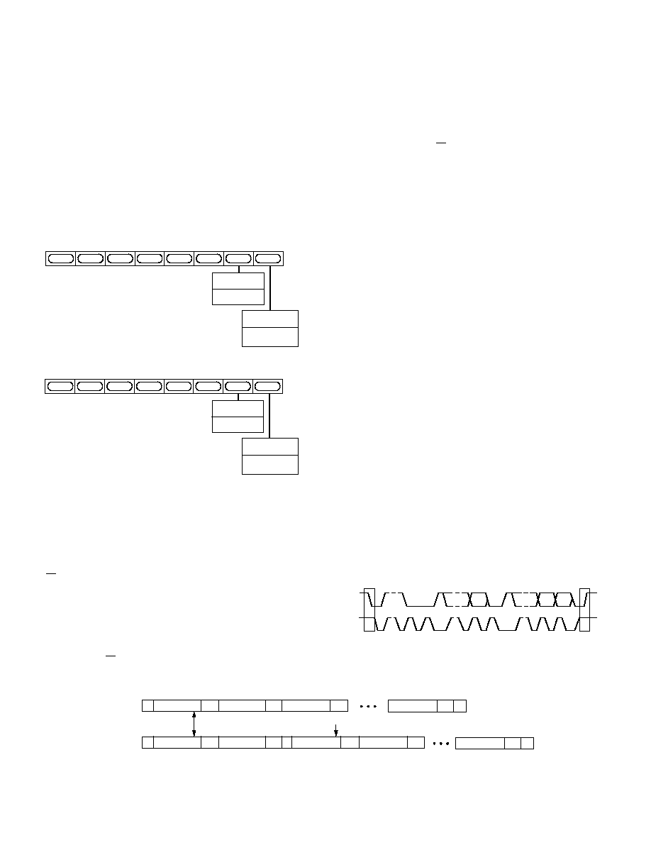
SUBCARRIER FREQUENCY REGISTERS 30 (FSC3FSC0)
(Address (SR4SR0) = 05H02H)
These 8-bit wide registers are used to set up the subcarrier fre-
quency. The value of these registers are calculated by using the
following equation:
Subcarrier Frequency Register =
2
32
1
F
CLK
* F
SCF
i.e.: NTSC Mode, F
CLK
= 27 MHz, F
SCF
= 3.5796 MHz
Subcarrier Frequency Register =
2
32
1
27
×
10
6
* 3.579545
×
10
6
Subcarrier Frequency Register
= 21F07C16 HEX
Figure 33 shows how the frequency is set up by the 4 registers.
SUBCARRIER
FREQUENCY
REG 0
SUBCARRIER
FREQUENCY
REG 1
SUBCARRIER
FREQUENCY
REG 2
SUBCARRIER
FREQUENCY
REG 3
FSC6
FSC5
FSC3
FSC1
FSC4
FSC2
FSC0
FSC7
FSC30 FSC29
FSC27
FSC25
FSC28
FSC26
FSC24
FSC31
FSC22 FSC21
FSC19
FSC17
FSC20
FSC18
FSC16
FSC23
FSC14 FSC13
FSC11
FSC9
FSC12
FSC10
FSC8
FSC15
Figure 33. Subcarrier Frequency Register
SUBCARRIER PHASE REGISTER (FP7FP0):
(Address (SR4SR0) = 06H)
This 8-bit wide register is used to set up the subcarrier phase.
Each bit represents 1.41
°
.
TIMING REGISTER 0 (TR07TR00)
(Address (SR4-SR0) = 07H)
Timing Register 0 is a 8-bit wide register.
Figure 34 shows the various operations under the control of
Timing Register 0. This register can be read from as well
written to.
TIMING REGISTER 0 (TR07TR00)
BIT DESCRIPTION
Master/Slave Control (TR00)
This bit controls whether the ADV7175/ADV7176 is in master
or slave mode.
Timing Mode Control (TR02TR01)
These bits control the timing mode of the ADV7175/ADV7176
These modes are described in the Timing and Control section
of the data sheet.
BLANK
Control (TR03)
This bit controls whether the BLANK input is used when the
part is in slave mode.
Luma Delay Control (TR05TR04)
These bits control the addition of a luminance delay. Each bit
represents a delay of 74 ns.
Pixel Port Select (TR06)
This bit is used to set the pixel port to accept 8-bit or 16-bit
data. If an 8-bit input is selected the data will be set up on
Pins P7P0.
Timing Register Reset (TR07)
Toggling TR07 from low to high and low again resets the inter-
nal timing counters. This bit should be toggled after setting up a
new timing mode.
TR01
TR00
TR07
TR02
TR03
TR05
TR06
TR04
TIMING
REGISTER RESET
TR07
BLACK INPUT
CONTROL
0
ENABLE
1
DISABLE
TR03
PIXEL PORT
CONTROL
0
8-BIT
1
16-BIT
TR06
MASTER/SLAVE
CONTROL
0
SLAVE TIMING
1
MASTER TIMING
TR00
LUMA DELAY
0
0
0ns DELAY
0
1
74ns DELAY
1
0
148ns DELAY
1
1
222ns DELAY
TR05 TR04
TIMING MODE
SELECTION
0
0
MODE 0
0
1
MODE 1
1
0
MODE 2
1
1
MODE 3
TR02 TR01
Figure 34. Timing Register 0
ADV7175/ADV7176
REV. A
20
HSYNC
to VSYNC/FIELD Delay Control (TR13TR12)
These bits adjust the position of the HSYNC output relative to
the FIELD/VSYNC output.
HSYNC
to FIELD Delay Control (TR15TR14)
When the ADV7175/ADV7176 is in Timing Mode 1, these bits
adjust the position of the HSYNC output relative to the FIELD
output rising edge.
VSYNC
Width (TR15TR14)
When the ADV7175/ADV7176 is in Timing Mode 2, these bits
adjust the VSYNC pulse width.
HSYNC
to Pixel Data Adjust (TR17TR16)
This enables the HSYNC to be adjusted with respect to the
pixel data. This allows the Cr and Cb components to be
swapped. This adjustment is available in both master and slave
timing modes.
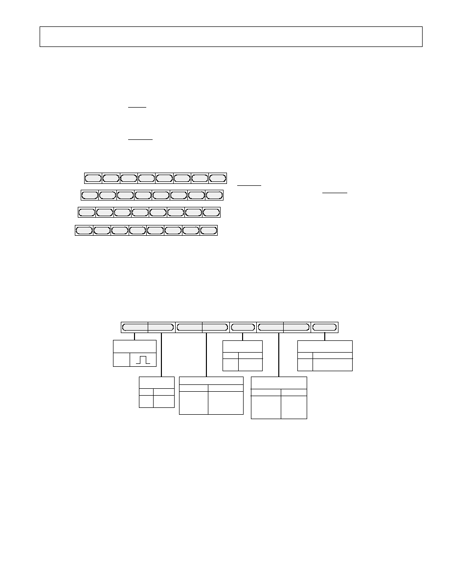
MODE REGISTER 2 MR2 (MR27MR20)
(Address (SR4-SR0) = 0DH)
Mode Register 2 is an 8-bit wide register.
Figure 38 shows the various operations under the control of
Mode Register 2. This register can be read from as well written to.
MODE REGISTER 2 (MR27MR20) BIT DESCRIPTION
Square Pixel Mode Control (MR20)
This bit is used to setup square pixel mode. This is available in
slave mode only. For NTSC, a 24.54 MHz clock must be sup-
plied. For PAL, a 29.5 MHz clock must be supplied.
Genlock Control (MR22MR21)
These bits control the genlock feature of the ADV7175/
ADV7176 Setting MR21 to a Logic "1" configures the
SCRESET/RTC pin as an input. Setting MR22 to logic level
"0" configures the SCRESET/RTC pin as a subcarrier reset in-
put. Therefore, the subcarrier will reset to Field 0 following a
low to high transition on the SCRESET/RTC pin. Setting
MR22 to Logic Level "1" configures the SCRESET/RTC pin as
a real time control input.
CLOSED CAPTIONING EXTENDED DATA REGISTERS
10 (CED15CED00)
(Address (SR4SR0) = 0908H)
These 8-bit wide registers are used to set up the closed
captioning extended data bytes. Figure 35 shows how the high
and low bytes are set up in the registers.
BYTE 1
BYTE 0
CED6
CED5
CED3
CED1
CED4
CED2
CED0
CED7
CED14 CED13
CED11
CED9
CED12
CED10
CED8
CED15
Figure 35. Closed Captioning Extended Data Register
CLOSED CAPTIONING DATA REGISTERS 10
(CCD15CCD00)
(Subaddress (SR4SR0) = 0B0AH)
These 8-bit wide registers are used to set up the closed
captioning data bytes. Figure 36 shows how the high and low
bytes are set up in the registers.
BYTE 1
BYTE 0
CCD6
CCD5
CCD3
CCD1
CCD4
CCD2
CCD0
CCD7
CCD14 CCD13
CCD11
CCD9
CCD12
CCD10
CCD8
CCD15
Figure 36. Closed Captioning Data Register
TIMING REGISTER 1 (TR17TR10)
(Address (SR4SR0) = 0CH)
Timing Register 1 is an 8-bit wide register.
Figure 37 shows the various operations under the control of
Timing Register 1. This register can be read from as well
written to. This register can be used to adjust the width and
position of the master mode timing signals.
TIMING REGISTER 1 (TR17TR10) BIT DESCRIPTION
HSYNC
Width (TR11TR10)
These bits adjust the HSYNC pulse width.
TR11
TR10
TR17
TR12
TR13
TR15
TR16
TR14
HSYNC
WIDTH
0
0
1 x T
PCLK
0
1
4 x T
PCLK
1
0
16 x T
PCLK
1
1
128 x T
PCLK
TR11 TR10
Ta
HSYNC
TO FIELD
RISING EDGE DELAY
(MODE 1 ONLY)
x
0
T
b
x
1
T
b
+ 32µs
TR15 TR14
Tc
HSYNC
TO PIXEL
DATA ADJUSTMENT
TR17 TR16
0
0
0 x T
PCLK
0
1
1 x T
PCLK
1
0
2 x T
PCLK
1
1
3 x T
PCLK
HSYNC
TO
FIELD/
VSYNC
DELAY
TR13 TR12
0
0
1 x T
PCLK
0
1
3 x T
PCLK
1
0
16 x T
PCLK
1
1
64 x T
PCLK
VSYNC
WIDTH
(MODE 2 ONLY)
TR15 TR14
0
0
1 x T
PCLK
0
1
4 x T
PCLK
1
0
16 x T
PCLK
1
1
64 x T
PCLK
LINE 313
LINE 314
LINE 1
Tb
TIMING MODE 1 (MASTER/PAL)
HSYNC
FIELD/
VSYNC
Ta
Tc
Figure 37. Timing Register 1
ADV7175/ADV7176
REV. A
21
MR21
MR27
MR22
MR23
MR26
MR25
MR24
MR20
CHROMINANCE
CONTROL
0
ENABLE COLOR
1
DISABLE COLOR
MR24
GENLOCK SELECTION
x
0
DISABLE GENLOCK
0
1
ENABLE SUBCARRIER
RESET PIN
1
1
ENABLE RTC PIN
MR22 MR21
RGB/YUV
CONTROL
0
RGB OUTPUT
1
YUV OUTPUT
MR26
SQUARE PIXEL
CONTROL
0
DISABLE
1
ENABLE
MR20
BURST
CONTROL
0
ENABLE BURST
1
DISABLE BURST
MR25
LOWER POWER
MODE
0
DISABLE
1
ENABLE
MR27
CCIR624/CCIR601
CONTROL
0
CCIR624 OUTPUT
1
CCIR601 OUTPUT
MR23
Figure 38. Mode Register 2
MR31
MR37
MR32
MR33
MR36
MR35
MR34
MR30
DAC OUTPUT
SWITCHING
MR37
DAC A
COMPOSITE
GREEN/LUMA/Y
0
1
DAC B
BLUE/COMP/U
BLUE/COMP/U
DAC C
RED/CHROMA/V
RED/CHROMA/V
DAC D
GREEN/LUMA/Y
COMPOSITE
MR36-MR30
(RESERVED)
ZERO SHOULD BE
WRITTEN TO THESE BITS
Figure 40. Mode Register 3
CCIR624/CCIR601 Control (MR23)
This bit switches the video output between CCIR624 and
CCIR601 video standard.
Chrominance Control (MR24)
This bit enables the color information to be switched on and off
the video output.
Burst Control (MR25)
This bit enables the burst information to be switched on and off
the video output.
RGB/YUV Control (MR26)
This bit enables the output from the RGB DACs to be set to
YUV output video standard. Bit MR06 of Mode Register 0
must be set to Logic Level "1" before MR26 is set.
Lower Power Control (MR27)
This bit enables the lower power mode of the ADV7175/
ADV7176.
NTSC PEDESTAL CONTROL REGISTERS 30
(PCE150, PCO150)
(Subaddress (SR4SR0) = 11-0EH)
These 8-bit wide registers are used to set up the NTSC pedestal
on a line by line basis in the vertical blanking interval for both
odd and even fields. Figure 39 shows the four control registers.
A Logic "1" in any of the bits of these registers has the effect of
turning the pedestal off on the equivalent line.
FIELD 1/3
PCO6
PCO5
PCO3
PCO1
PCO4
PCO2
PCO0
PCO7
LINE 17 LINE 16 LINE 15 LINE 14 LINE 13 LINE 12 LINE 11 LINE 10
PCO14
PCO13
PCO11
PCO9
PCO12
PCO10
PCO8
PCO15
LINE 25 LINE 24 LINE 23 LINE 22 LINE 21 LINE 20 LINE 19 LINE 18
FIELD 1/3
FIELD 2/4
PCE6
PCE5
PCE3
PCE1
PCE4
PCE2
PCE0
PCE7
LINE 17 LINE 16 LINE 15 LINE 14 LINE 13 LINE 12 LINE 11 LINE 10
PCE14
PCE13
PCE11
PCE9
PCE12
PCE10
PCE8
PCE15
LINE 25 LINE 24 LINE 23 LINE 22 LINE 21 LINE 20 LINE 19 LINE 18
FIELD 2/4
Figure 39. Pedestal Control Registers
MODE REGISTER 3 MR3 (MR3730)
(Address (SR4SR0) = 12H)
Mode Register 3 is an 8-bit wide register.
Figure 34 shows the various operations under the control of
Mode Register 3. Bits MR36MR30 are reserved and Logic "0"
should be written to them.
MODE REGISTER 3 (MR37MR30) DESCRIPTION
DAC Switching Control (MR37)
This bit is used to switch the luminance signal onto the compos-
ite DAC. Figure 40 illustrates the DAC outputs and how they
switch when MR 37 is set to Logic "1".

ADV7175/ADV7176
REV. A
22
APPENDIX 1
BOARD DESIGN AND LAYOUT CONSIDERATIONS
operation, to reduce the lead inductance. Best performance is
obtained with 0.1
µ
F ceramic capacitor decoupling. Each group
of V
AA
pins on the ADV7175/ADV7176 must have at least one
0.1
µ
F decoupling capacitor to GND. These capacitors should
be placed as close as possible to the device.
It is important to note that while the ADV7175/ADV7176
contains circuitry to reject power supply noise, this rejection
decreases with frequency. If a high frequency switching power
supply is used, the designer should pay close attention to reduc-
ing power supply noise and consider using a three terminal volt-
age regulator for supplying power to the analog power plane.
Digital Signal Interconnect
The digital inputs to the ADV7175/ADV7176 should be iso-
lated as much as possible from the analog outputs and other
analog circuitry. Also, these input signals should not overlay
the analog power plane.
Due to the high clock rates involved, long clock lines to the
ADV7175/ADV7176 should be avoided to reduce noise pickup.
Any active termination resistors for the digital inputs should be
connected to the regular PCB power plane (V
CC
), and not the
analog power plane.
Analog Signal Interconnect
The ADV7175/ADV7176 should be located as close as possible
to the output connectors to minimize noise pickup and reflec-
tions due to impedance mismatch.
The video output signals should overlay the ground plane, and
not the analog power plane, to maximize the high frequency
power supply rejection.
Digital inputs, especially pixel data inputs and clocking signals
should never overlay any of the analog signal circuitry and
should be kept as far away as possible.
For best performance, the outputs should each have a 75
load resistor connected to GND. These resistors should be
placed as close as possible to the ADV7175/ADV7176 so as to
minimize reflections.
The ADV7175/ADV7176 should have no inputs left floating.
Any inputs that are not required should be tied to ground.
The ADV7175/ADV7176 is a highly integrated circuit contain-
ing both precision analog and high speed digital circuitry. It has
been designed to minimize interference effects on the integrity
of the analog circuitry by the high speed digital circuitry. It is
imperative that these same design and layout techniques be ap-
plied to the system level design such that high speed, accurate
performance is achieved. The "Recommended Analog Circuit
Layout" shows the analog interface between the device and
monitor.
The layout should be optimized for lowest noise on the
ADV7175/ADV7176 power and ground lines by shielding the
digital inputs and providing good decoupling. The lead length
between groups of V
AA
and GND pins should by minimized so
as to minimize inductive ringing.
Ground Planes
The ground plane should encompass all ADV7175/ADV7176
ground pins, voltage reference circuitry, power supply bypass
circuitry for the ADV7175/ADV7176, the analog output traces,
and all the digital signal traces leading up to the ADV7175/
ADV7176. The ground plane is the board's common ground
plane.
Power Planes
The ADV7175/ADV7176 and any associated analog circuitry
should have its own power plane, referred to as the analog
power plane (V
AA
). This power plane should be connected to
the regular PCB power plane (V
CC
) at a single point through a
ferrite bead. This bead should be located within three inches of
the ADV7175/ADV7176.
The PCB power plane should provide power to all digital logic
on the PC board, and the analog power plane should provide
power to all ADV7175/ADV7176 power pins and voltage refer-
ence circuitry.
Plane-to-plane noise coupling can be reduced by ensuring that
portions of the regular PCB power and ground planes do not
overlay portions of the analog power plane, unless they can be
arranged such that the plane-to-plane noise is common mode.
Supply Decoupling
For optimum performance, bypass capacitors should be in-
stalled using the shortest leads possible, consistent with reliable
ADV7175/ADV7176
REV. A
23
75
27
26
S VIDEO
31
32
5k
+5V (V
CC
)
150
24
5k
+5V (V
CC
)
MPU BUS
44
22
15
17
16
10, 19, 21
29, 36, 43
18
23
34
3842,
29, 1214
1, 11, 20, 28, 30, 37
0.1µF
0.01µF
0.1µF
+5V (V
AA
)
0.1µF
+5V (V
AA
)
10k
+5V (V
AA
)
27MHz CLOCK
(SAME CLOCK AS USED BY
MPEG2 DECODER)
POWER SUPPLY DECOUPLING
FOR EACH POWER SUPPLY GROUP
10µF
33µF
GND
L1
(FERRITE BEAD)
+5V (V
CC
)
25
33
GND
ALSB
HSYNC
FIELD/
VSYNC
BLANK
RESET
CLOCK
R
SET
SDATA
SCLOCK
COMPOSITE
BLUE/
COMPOSITE/
U
RED/
CHROMA/
V
GREEN/
LUMA/
Y
V
AA
V
REF
COMP
P15P0
+5V (V
AA
)
75
75
75
35 SCRESET/RTC
ADV7175
ADV7176
"UNUSED
INPUTS
SHOULD BE
GROUNDED"
Figure 41. Recommended Analog Circuit Layout
The circuit below can be used to generate a 13.5 MHz waveform using the 27 MHz clock and the HSYNC pulse. This waveform is
guaranteed to produce the 13.5 MHz clock in synchronization with the 27 MHz clock. This 13.5 MHz clock can be used if
13.5 MHz clock is required by the MPEG decoder. This will guarantee that the Cr and Cb pixel information is input to the
ADV7175/ADV7176 in the correct sequence.
D
Q
CK
D
Q
CK
CLOCK
HSYNC
13.5MHz
Figure 42. Circuit to Generate 13.5 MHz
ADV7175/ADV7176
REV. A
24
APPENDIX 2
CLOSED CAPTIONING
The ADV7175/ADV7176 supports closed captioning conforming to the standard television synchronizing waveform for color trans-
mission. Closed captioning is transmitted during the blanked active line time of line 21 of the odd fields.
Closed captioning consists of a 7-cycle sinusoidal burst that is frequency and phase locked to the caption data. After the clock run in
signal, the blanking level is held for two data bits and is followed by a Logic Level "1" start bit. Sixteen bits of data follow the start
bit. These consist of two 8-bit bytes. The data for these bytes is stored in closed captioning data registers 0 and 1.
The ADV7175/ADV7176 also supports the extended closed captioning operation which is active during even fields and is encoded
on scan line 284. The data for this operation is stored in closed captioning extended data registers 0 and 1.
All clock run-in signals and timing to support closed captioning on lines 21 and 282 are generated automatically by the ADV7175/
ADV7176. All pixels inputs are ignored during lines 21 and 282.
FCC Code of Federal Regulations (CFR) 47 section 15.119 and EIA208 describe the closed captioning information for lines
21 and 284.
13.407µs
S
T
A
R
T
P
A
R
I
T
Y
P
A
R
I
T
Y
D6D0
D6D0
10.003µs
17.379µs
33.764µs
50 IRE
40 IRE
FREQUENCY = F
SC
= 3.579545MHz
AMPLITUDE = 40 IRE
REFERENCE COLOR BURST
(9 CYCLES)
Figure 43. Closed Captioning Waveform (NTSC)
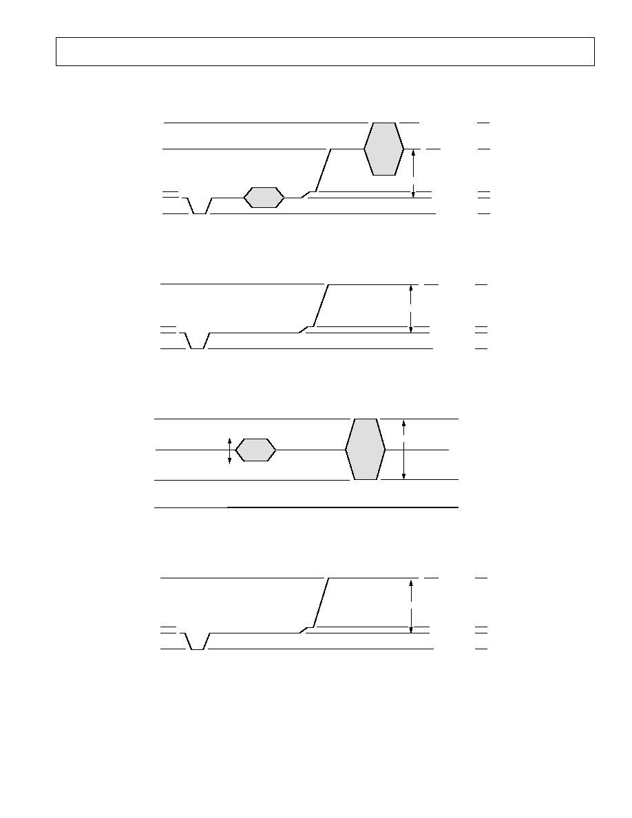
ADV7175/ADV7176
REV. A
25
APPENDIX 3
NTSC WAVEFORMS (With Pedestal)
130.8 IRE
100 IRE
7.5 IRE
0 IRE
40 IRE
PEAK COMPOSITE
REF WHITE
BLACK LEVEL
SYNC LEVEL
BLANK LEVEL
714.2mV
1268.1mV
1048.4mV
387.6mV
334.2mV
48.3mV
Figure 44. NTSC Composite Video Levels
100 IRE
7.5 IRE
0 IRE
40 IRE
REF WHITE
BLACK LEVEL
SYNC LEVEL
BLANK LEVEL
714.2mV
1048.4mV
387.6mV
334.2mV
48.3mV
Figure 45. NTSC Luma Video Levels
650mV
232.2mV
1067.7mV
0mV
PEAK CHROMA
BLANK/BLACK LEVEL
286mV (pk-pk)
835mV (pk-pk)
PEAK CHROMA
Figure 46. NTSC Chroma Video Levels
100 IRE
7.5 IRE
0 IRE
40 IRE
REF WHITE
BLACK LEVEL
SYNC LEVEL
BLANK LEVEL
720.8mV
1052.2mV
387.5mV
331.4mV
45.9mV
Figure 47. NTSC RGB Video Levels
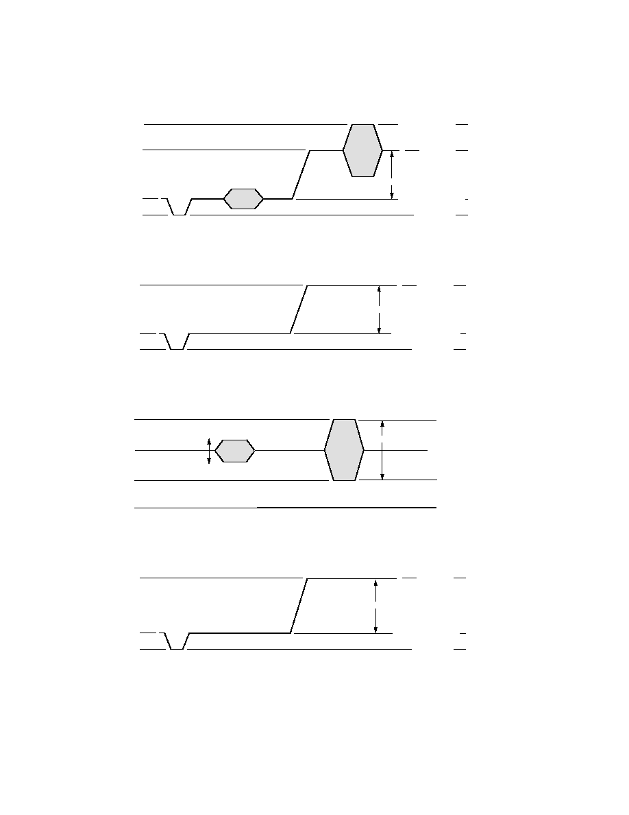
ADV7175/ADV7176
REV. A
26
NTSC WAVEFORMS (Without Pedestal)
130.8 IRE
100 IRE
0 IRE
40 IRE
PEAK COMPOSITE
REF WHITE
SYNC LEVEL
BLANK/BLACK LEVEL
714.2mV
1289.8mV
1052.2mV
338mV
52.1mV
Figure 48. NTSC Composite Video Levels
100 IRE
0 IRE
40 IRE
REF WHITE
SYNC LEVEL
BLANK /BLACK LEVEL
714.2mV
1052.2mV
338mV
52.1mV
Figure 49. NTSC Luma Video Levels
650mV
198.4mV
1101.6mV
0mV
PEAK CHROMA
BLANK/BLACK LEVEL
307mV (pk-pk)
903.2mV (pk-pk)
PEAK CHROMA
Figure 50. NTSC Chroma Video Levels
100 IRE
0 IRE
40 IRE
REF WHITE
SYNC LEVEL
BLANK/BLACK LEVEL
715.7mV
1052.2mV
336.5mV
51mV
Figure 51. NTSC RGB Video Levels
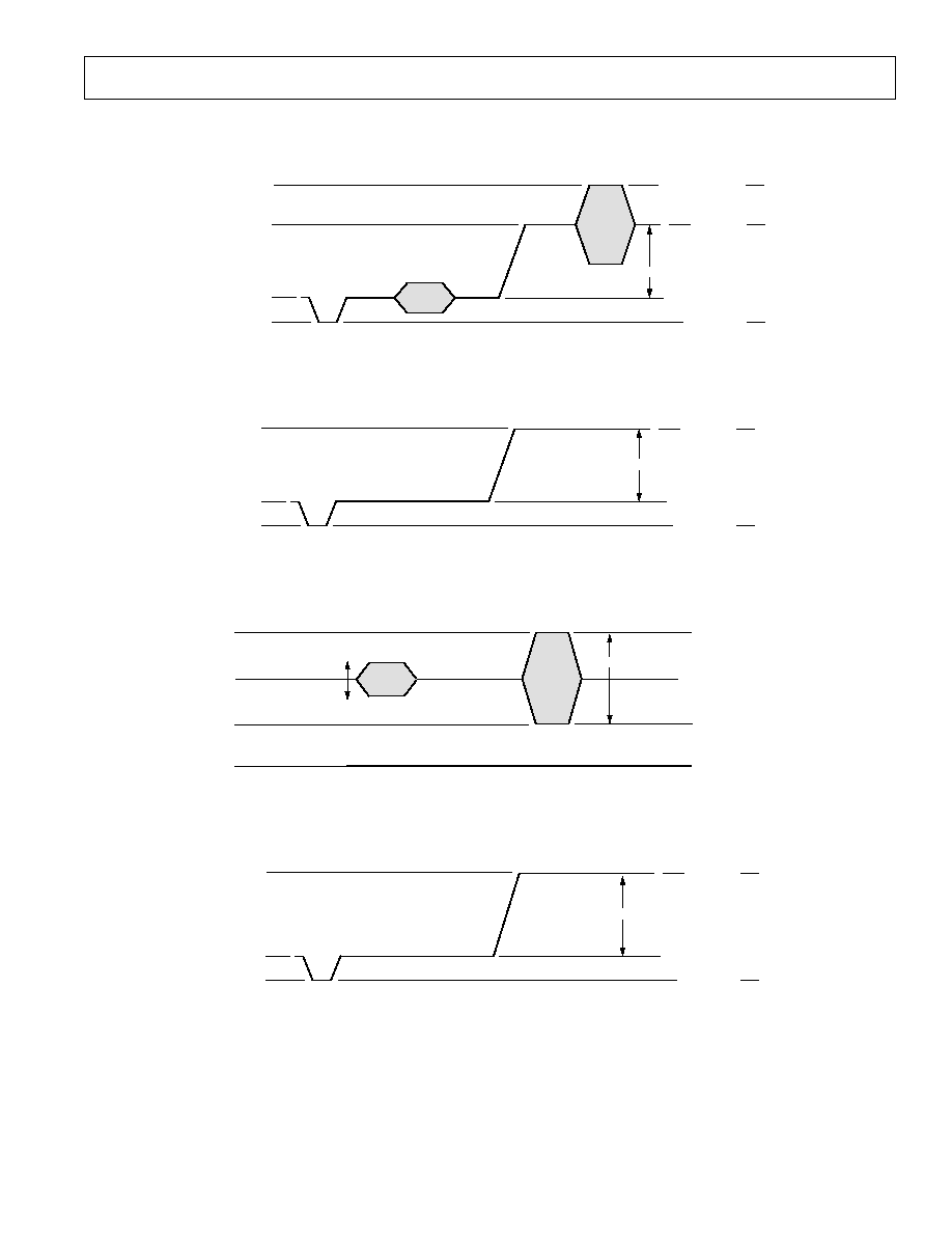
ADV7175/ADV7176
REV. A
27
PAL WAVEFORMS
1284.2mV
1047.1mV
350.7mV
50.8mV
PEAK COMPOSITE
REF WHITE
SYNC LEVEL
BLANK/BLACK LEVEL
696.4mV
Figure 52. PAL Composite Video Levels
1047mV
350.7mV
50.8mV
REF WHITE
SYNC LEVEL
BLANK/BLACK LEVEL
696.4mV
Figure 53. PAL Luma Video Levels
650mV
207.5mV
1092.5mV
0mV
PEAK CHROMA
BLANK/BLACK LEVEL
300mV (pk-pk)
885mV (pk-pk)
PEAK CHROMA
Figure 54. PAL Chroma Video Levels
1050.2mV
351.8mV
51mV
REF WHITE
SYNC LEVEL
BLANK /BLACK LEVEL
698.4mV
Figure 55. PAL RGB Video Levels

ADV7175/ADV7176
REV. A
28
APPENDIX 4
REGISTER VALUES
PAL (M)
Mode Register 0
06 Hex
Mode Register 1
00 Hex
Subcarrier Frequency Register 0
A3 Hex
Subcarrier Frequency Register 1
EF Hex
Subcarrier Frequency Register 2
E6 Hex
Subcarrier Frequency Register 3
21 Hex
Subcarrier Phase Register
00 Hex
Timing Register 0
08 Hex
Closed Captioning Ext Register 0
00 Hex
Closed Captioning Ext Register 1
00 Hex
Closed Captioning Register 0
00 Hex
Closed Captioning Register 1
00 Hex
Timing Register 1
00 Hex
Mode Register 2
00 Hex
Pedestal Control Register 0
00 Hex
Pedestal Control Register 1
00 Hex
Pedestal Control Register 2
00 Hex
Pedestal Control Register 3
00 Hex
Mode Register 3
00 Hex
PAL (N)
Mode Register 0
05 Hex
Mode Register 1
00 Hex
Subcarrier Frequency Register 0
CB Hex
Subcarrier Frequency Register 1
8A Hex
Subcarrier Frequency Register 2
09 Hex
Subcarrier Frequency Register 3
2A Hex
Subcarrier Phase Register
00 Hex
Timing Register 0
08 Hex
Closed Captioning Ext Register 0
00 Hex
Closed Captioning Ext Register 1
00 Hex
Closed Captioning Register 0
00 Hex
Closed Captioning Register 1
00 Hex
Timing Register 1
00 Hex
Mode Register 2
00 Hex
Pedestal Control Register 0
00 Hex
Pedestal Control Register 1
00 Hex
Pedestal Control Register 2
00 Hex
Pedestal Control Register 3
00 Hex
Mode Register 3
00 Hex
The ADV7175/ADV7176 registers can be set depending on the
user standard required.
The following examples give the various register formats for
several video standards.
In each case the output is set to composite o/p with all DACs
powered up and with the BLANK input control disabled. Ad-
ditionally, the burst and color information are enabled on the
output and the internal color bar generator is switched off. In
the examples shown the timing mode is set to Mode 0 in slave
format. TR02TR00 of the timing register 0 control the timing
modes. For a detailed explanation of each bit in the command
registers, please turn to the register programming section of the
data sheet. TR07 should be toggled after setting up a new tim-
ing mode. Timing Register 1 provides additional control over
the position and duration of the timing signals. In the examples
this register is programmed in default mode.
NTSC
Mode Register 0
04 Hex
Mode Register 1
00 Hex
Subcarrier Frequency Register 0
16 Hex
Subcarrier Frequency Register 1
7C Hex
Subcarrier Frequency Register 2
F0 Hex
Subcarrier Frequency Register 3
21 Hex
Subcarrier Phase Register
00 Hex
Timing Register 0
08 Hex
Closed Captioning Ext Register 0
00 Hex
Closed Captioning Ext Register 1
00 Hex
Closed Captioning Register 0
00 Hex
Closed Captioning Register 1
00 Hex
Timing Register 1
00 Hex
Mode Register 2
00 Hex
Pedestal Control Register 0
00 Hex
Pedestal Control Register 1
00 Hex
Pedestal Control Register 2
00 Hex
Pedestal Control Register 3
00 Hex
Mode Register 3
00 Hex
PAL (B, D, G, H, I)
Mode Register 0
01 Hex
Mode Register 1
00 Hex
Subcarrier Frequency Register 0
CB Hex
Subcarrier Frequency Register 1
8A Hex
Subcarrier Frequency Register 2
09 Hex
Subcarrier Frequency Register 3
2A Hex
Subcarrier Phase Register
00 Hex
Timing Register 0
08 Hex
Closed Captioning Ext Register 0
00 Hex
Closed Captioning Ext Register 1
00 Hex
Closed Captioning Register 0
00 Hex
Closed Captioning Register 1
00 Hex
Timing Register 1
00 Hex
Mode Register 2
00 Hex
Pedestal Control Register 0
00 Hex
Pedestal Control Register 1
00 Hex
Pedestal Control Register 2
00 Hex
Pedestal Control Register 3
00 Hex
Mode Register 3
00 Hex
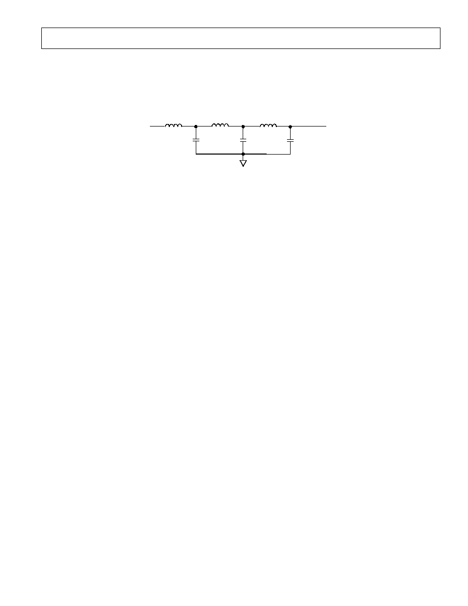
ADV7175/ADV7176
REV. A
29
APPENDIX 5
OUTPUT FILTER
If an output filter is required for the composite output of the ADV7175/ADV7176. The following filter can be used.
Plots of the filter characteristics can be produced on request.
L
1µH
C
470pF
L
2.7µH
C
330pF
C
56pF
L
0.7µH
IN
OUT
Figure 56. Output Filter
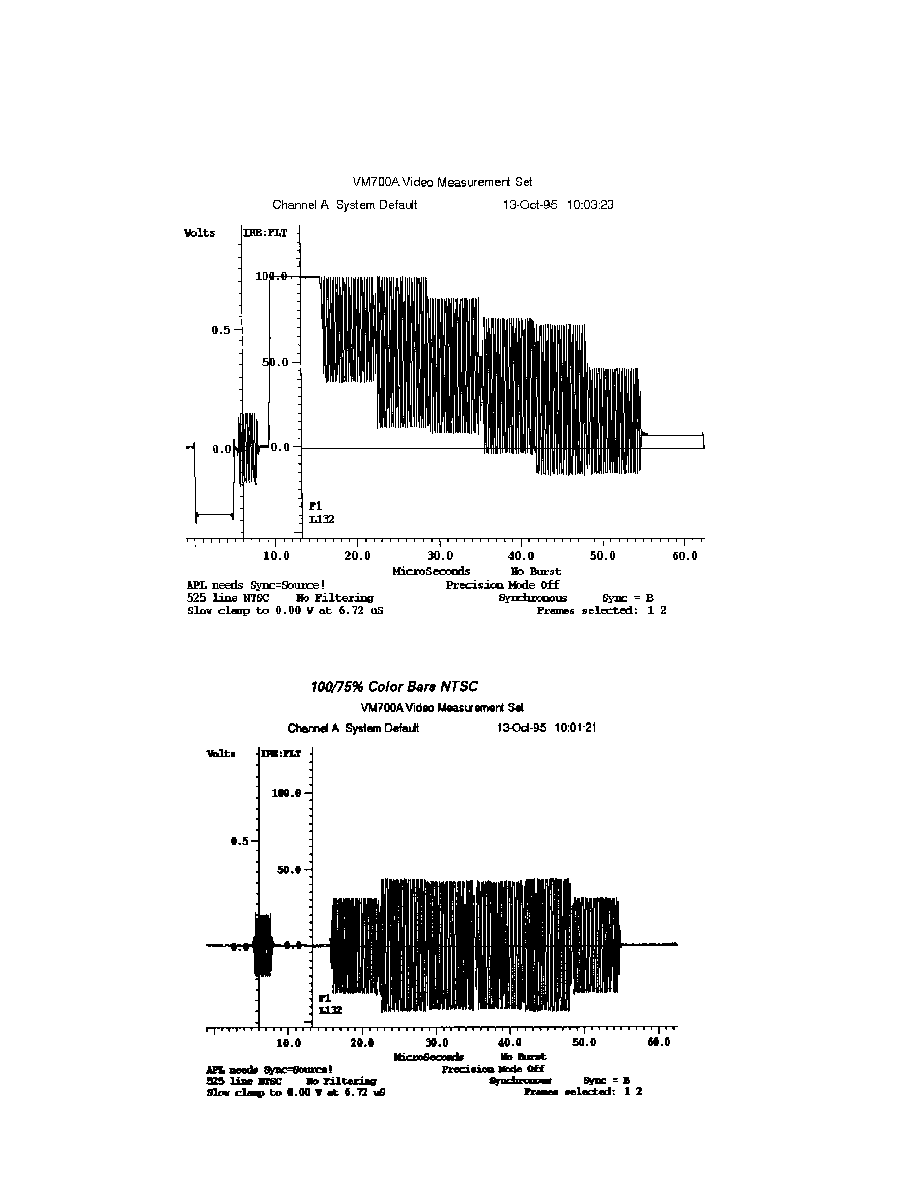
ADV7175/ADV7176
REV. A
30
APPENDIX 6
OUTPUT WAVEFORMS
Figure 57. 100/75% Color Bars NTSC
Figure 58. 100/75% Color Bars NTSC (Chrominance Only)
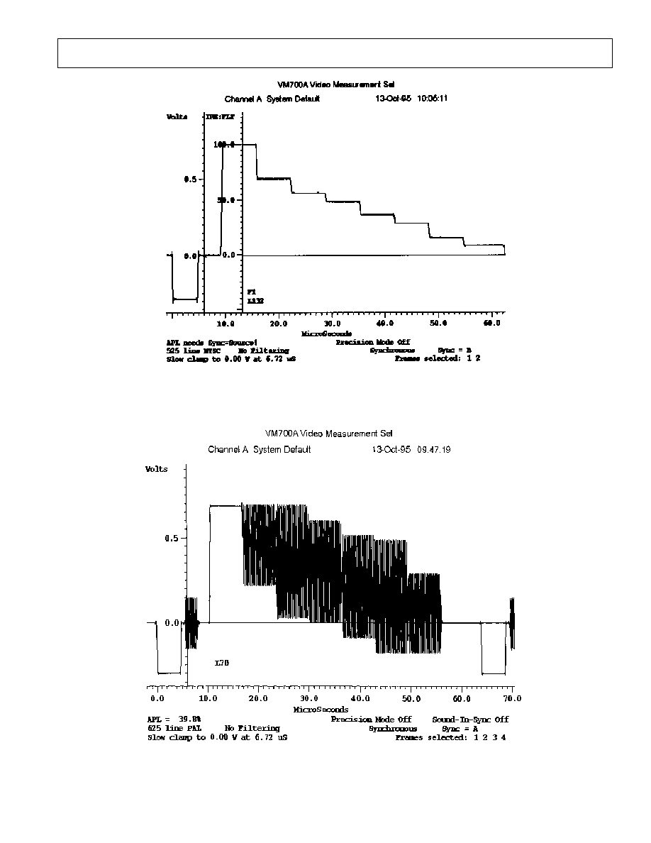
ADV7175/ADV7176
REV. A
31
Figure 59. 100/75% Color Bars NTSC (Luminance Only)
Figure 60. 100/75% Color Bars PAL
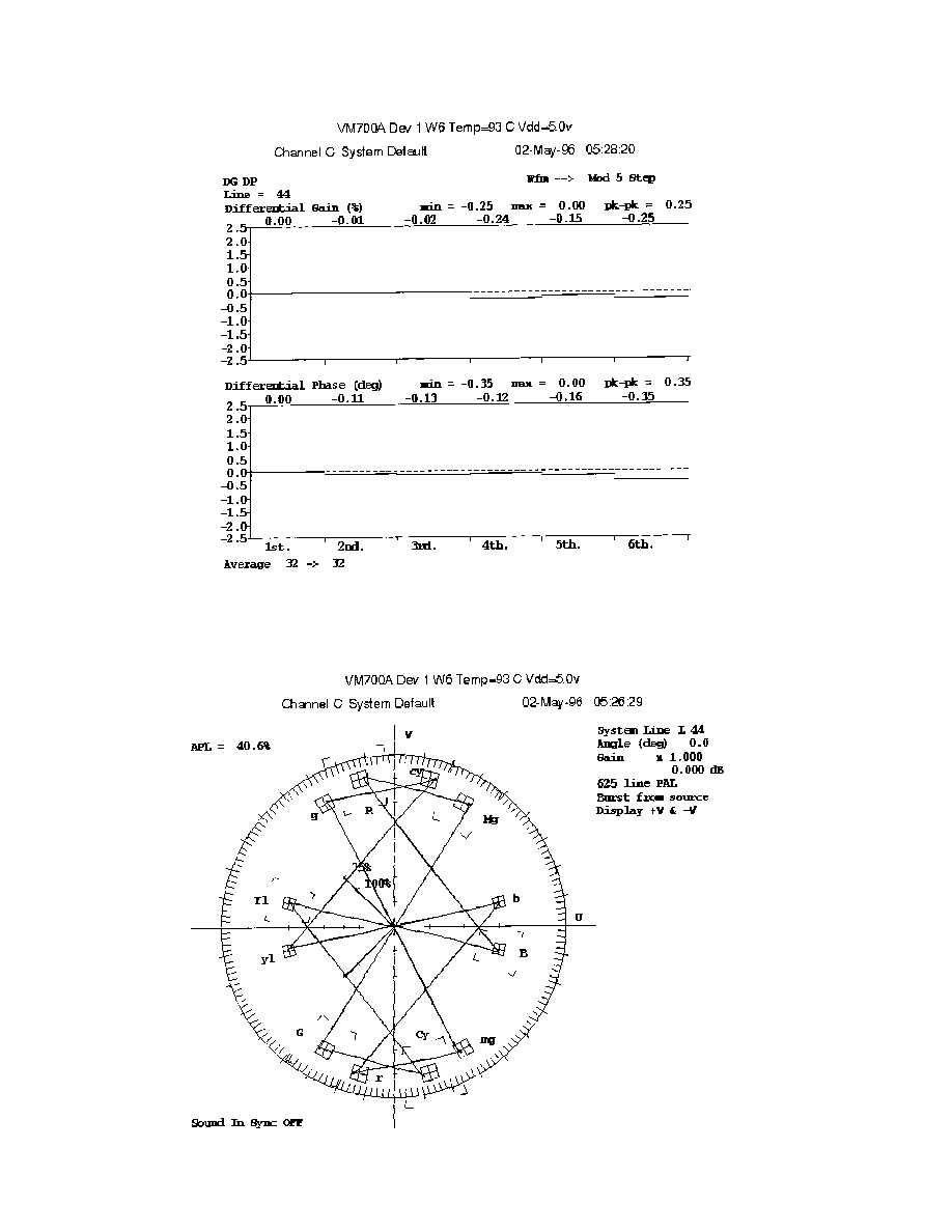
ADV7175/ADV7176
REV. A
32
Figure 61. Differential Phase and Gain Measurements (PAL)
Figure 62. Vectorscope Measurements (PAL)
ADV7175/ADV7176
REV. A
33
Figure 63. Modulated Ramp Measurements (PAL)

ADV7175/ADV7176
REV. A
34
INDEX
Contents
Page No.
GENERAL DESCRIPTION . . . . . . . . . . . . . . . . . . . . . . . . 1
ADV7175/ADV7176 SPECIFICATIONS . . . . . . . . . . . . . . 2
TIMING SPECIFICATIONS . . . . . . . . . . . . . . . . . . . . . . 3
ABSOLUTE MAXIMUM RATINGS . . . . . . . . . . . . . . . . . 4
ORDERING GUIDE . . . . . . . . . . . . . . . . . . . . . . . . . . . . . 4
PIN DESCRIPTION/PIN CONFIGURATION . . . . . . . . . 5
DATA PATH DESCRIPTION . . . . . . . . . . . . . . . . . . . . . . 6
INTERNAL FILTER RESPONSE . . . . . . . . . . . . . . . . . . . 6
COLOR BAR GENERATION . . . . . . . . . . . . . . . . . . . . . . 8
SQUARE PIXEL MODE . . . . . . . . . . . . . . . . . . . . . . . . . . 8
COLOR SIGNAL CONTROL . . . . . . . . . . . . . . . . . . . . . . 8
BURST SIGNAL CONTROL . . . . . . . . . . . . . . . . . . . . . . 8
NTSC PEDESTAL CONTROL . . . . . . . . . . . . . . . . . . . . . 8
SUBCARRIER RESET . . . . . . . . . . . . . . . . . . . . . . . . . . . . 8
REAL TIME CONTROL . . . . . . . . . . . . . . . . . . . . . . . . . . 8
PIXEL TIMING DESCRIPTION . . . . . . . . . . . . . . . . . . . 8
VIDEO TIMING DESCRIPTION . . . . . . . . . . . . . . . . . . . 8
Timing Mode 0 . . . . . . . . . . . . . . . . . . . . . . . . . . . . . . . . 9
Timing Mode 1 . . . . . . . . . . . . . . . . . . . . . . . . . . . . . . . 11
Timing Mode 2 . . . . . . . . . . . . . . . . . . . . . . . . . . . . . . . 12
Timing Mode 3 . . . . . . . . . . . . . . . . . . . . . . . . . . . . . . . 14
OUTPUT VIDEO TIMING . . . . . . . . . . . . . . . . . . . . . . . 15
POWER-ON RESET . . . . . . . . . . . . . . . . . . . . . . . . . . . . 15
MPU PORT DESCRIPTION . . . . . . . . . . . . . . . . . . . . . . 16
Contents
Page No.
REGISTER ACCESSES . . . . . . . . . . . . . . . . . . . . . . . . . . 17
REGISTER PROGRAMMING . . . . . . . . . . . . . . . . . . . . 17
Subaddress Register . . . . . . . . . . . . . . . . . . . . . . . . . . . . 17
Mode Register 0 . . . . . . . . . . . . . . . . . . . . . . . . . . . . . . . 17
Mode Register 1 . . . . . . . . . . . . . . . . . . . . . . . . . . . . . . . 18
Subcarrier Frequency Registers . . . . . . . . . . . . . . . . . . . 19
Subcarrier Phase Register . . . . . . . . . . . . . . . . . . . . . . . . 19
Timing Register 0 . . . . . . . . . . . . . . . . . . . . . . . . . . . . . . 19
Closed Captioning Extended Data Registers 1-0 . . . . . . 20
Closed Captioning Data Registers 1-0 . . . . . . . . . . . . . . 20
Timing Register 1 . . . . . . . . . . . . . . . . . . . . . . . . . . . . . . 20
Mode Register 2 . . . . . . . . . . . . . . . . . . . . . . . . . . . . . . . 20
NTSC Pedestal Control Registers 3-0 . . . . . . . . . . . . . . 21
APPENDIX 1. BOARD DESIGN AND LAYOUT
CONSIDERATIONS . . . . . . . . . . . . . . . . . . . . . . . . . . 22
APPENDIX 2. CLOSED CAPTIONING . . . . . . . . . . . . 24
APPENDIX 3. VIDEO WAVEFORMS . . . . . . . . . . . . . . 25
APPENDIX 4. REGISTER VALUES . . . . . . . . . . . . . . . 28
APPENDIX 5. OUTPUT FILTER . . . . . . . . . . . . . . . . . 29
APPENDIX 6. OUTPUT WAVEFORMS . . . . . . . . . . . . 30
OUTLINE DIMENSIONS . . . . . . . . . . . . . . . . . . . . . . . . 35
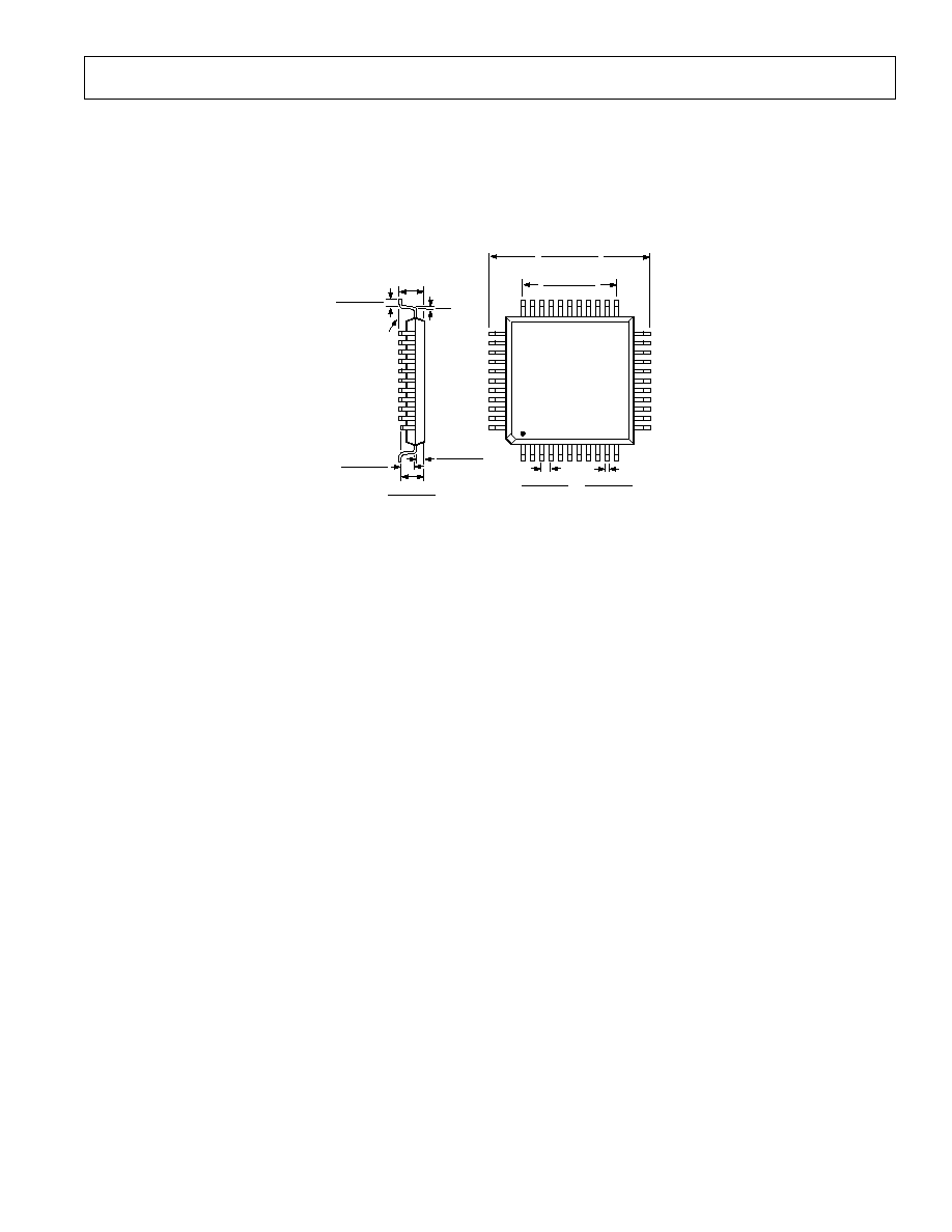
ADV7175/ADV7176
REV. A
35
OUTLINE DIMENSIONS
Dimensions shown in inches and (mm).
Plastic Quad Flatpack
(S-44)
0.548 (13.925)
0.546 (13.875)
TOP VIEW
(PINS DOWN)
1
33
34
4
4
11
12
23
22
0.033 (0.84)
0.029 (0.74)
0.398 (10.11)
0.390 (9.91)
0.016 (0.41)
0.012 (0.30)
0.083 (2.11)
0.077 (1.96)
0.040 (1.02)
0.032 (0.81)
0.040 (1.02)
0.032 (0.81)
SEATING
PLANE
0.096 (2.44)
MAX
0.037 (0.94)
0.025 (0.64)
8
°
0.8
°

C213a4
/96
PRINTED IN U.S.A.
36