 | ÐлекÑÑоннÑй компоненÑ: ADV7176A | СкаÑаÑÑ:  PDF PDF  ZIP ZIP |
Äîêóìåíòàöèÿ è îïèñàíèÿ www.docs.chipfind.ru
REV. B
Information furnished by Analog Devices is believed to be accurate and
reliable. However, no responsibility is assumed by Analog Devices for its
use, nor for any infringements of patents or other rights of third parties
which may result from its use. No license is granted by implication or
otherwise under any patent or patent rights of Analog Devices.
a
ADV7175A/ADV7176A*
One Technology Way, P.O. Box 9106, Norwood, MA 02062-9106, U.S.A.
Tel: 781/329-4700
World Wide Web Site: http://www.analog.com
Fax: 781/326-8703
© Analog Devices, Inc., 1998
High Quality, 10-Bit, Digital CCIR-601
to PAL/NTSC Video Encoder
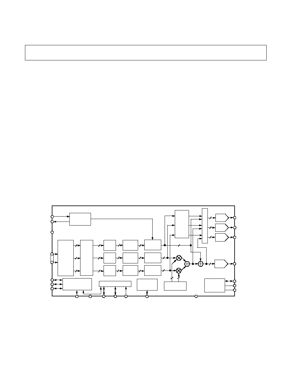
FUNCTIONAL BLOCK DIAGRAM
FEATURES
ITU-R BT601/656 YCrCb to PAL/NTSC Video Encoder
High Quality 10-Bit Video DACs
Integral Nonlinearity <1 LSB at 10 Bits
NTSC-M, PAL-M/N, PAL-B/D/G/H/I
Single 27 MHz Clock Required ( 2 Oversampling)
80 dB Video SNR
32-Bit Direct Digital Synthesizer for Color Subcarrier
Multistandard Video Output Support:
Composite (CVBS)
Component S-Video (Y/C)
Component YUV and RGB
EuroSCART Output (RGB + CVBS/LUMA)
Video Input Data Port Supports:
CCIR-656 4:2:2 8-Bit Parallel Input Format
4:2:2 16-Bit Parallel Input Format
SMPTE 170M NTSC Compatible Composite Video
ITU-R BT.470 PAL Compatible Composite Video
Full Video Output Drive or Low Signal Drive Capability
34.7 mA max into 37.5 (Doubly-Terminated 75R)
5 mA min with External Buffers
Programmable Simultaneous Composite
and S-Video Y/C or RGB (SCART)/YUV Video Outputs
Programmable Luma Filters (Low-Pass/Notch/Extended)
Programmable VBI (Vertical Blanking Interval)
Programmable Subcarrier Frequency and Phase
Programmable LUMA Delay
Individual ON/OFF Control of Each DAC
CCIR and Square Pixel Operation
Integrated Subcarrier Locking to External Video Source
Color Signal Control/Burst Signal Control
Interlaced/Noninterlaced Operation
Complete On-Chip Video Timing Generator
Programmable Multimode Master/Slave Operation
Macrovision Antitaping Rev 7.01 (ADV7175A Only)**
Closed Captioning Support
Teletext Insertion Port (PAL-WST)
Onboard Color Bar Generation
Onboard Voltage Reference
2-Wire Serial MPU Interface (I
2
C Compatible)
Single Supply +5 V or + 3 V Operation
Small 44-Lead PQFP Thermally Enhanced Package
APPLICATIONS
MPEG-1 and MPEG-2 Video, DVD, Digital Satellite/
Cable Systems (Set Top Boxes/IRDs), Digital TVs,
CD Video/Karaoke, Video Games, PC Video/Multimedia
*Protected by U.S. patents numbers 5,343,196 and 5,442,355 and other intellectual property rights.
**This device is protected by U.S. Patent Numbers 4631603, 4577216, 4819098 and other intellectual property rights. The Macrovision anticopy process is
licensed for noncommercial home use only, which is its sole intended use in the device. Please contact sales office for latest Macrovision version available.
NOTE: ITU-R and CCIR are used interchangeably in this document (ITU-R has replaced CCIR recommendations).
(Continued on page 11)
GENERAL DESCRIPTION
The ADV7175A/ADV7176A is an integrated digital video en-
coder that converts Digital CCIR-601 4:2:2 8 or 16-bit compo-
nent video data into a standard analog baseband television
YUV TO
RBG
MATRIX
V
AA
8
8
8
10
8
8
8
10
8
8
8
10
INTER-
POLATOR
YCrCb
TO
YUV
MATRIX
SIN/COS
DDS BLOCK
10
10
10
10
10
10
M
U
L
T
I
P
L
E
X
E
R
VIDEO TIMING
GENERATOR
I
2
C MPU PORT
4:2:2 TO
4:4:4
INTER-
POLATOR
VOLTAGE
REFERENCE
CIRCUIT
SCLOCK SDATA ALSB
HSYNC
FIELD/
VSYNC
BLANK
CLOCK
GND
DAC D (PIN 27)
DAC A (PIN 32)
V
REF
R
SET
COMP
V
LOW-PASS
FILTER
ADD
BURST
8
8
8
ADV7175A/ADV7176A
10-BIT
DAC
COLOR
DATA
P7P0
P15P8
10-BIT
DAC
10-BIT
DAC
REAL-TIME
CONTROL
CIRCUIT
SCRESET/RTC
INTER-
POLATOR
ADD
BURST
INTER-
POLATOR
ADD
SYNC
U
LOW-PASS
FILTER
Y
LOW-PASS
FILTER
10-BIT
DAC
DAC C (PIN 26)
DAC B (PIN 31)
TELETEXT
INSERTION
BLOCK
TTXREQ
TTX
RESET

2
REV. B
ADV7175A/ADV7176ASPECIFICATIONS
(V
AA
= +5 V 5%
1
, V
REF
= 1.235 V R
SET
= 150 . All specifications T
MIN
to T
MAX
2
unless otherwise noted)
Parameter
Conditions
1
Min
Typ
Max
Units
STATIC PERFORMANCE
Resolution (Each DAC)
10
Bits
Accuracy (Each DAC)
Integral Nonlinearity
±
1
LSB
Differential Nonlinearity
Guaranteed Monotonic
±
1
LSB
DIGITAL INPUTS
Input High Voltage, V
INH
2
V
Input Low Voltage, V
INL
0.8
V
Input Current, I
IN
3
V
IN
= 0.4 V or 2.4 V
±
1
µ
A
Input Current, I
IN
4
V
IN
= 0.4 V or 2.4 V
±
50
µ
A
Input Capacitance, C
IN
10
pF
DIGITAL OUTPUTS
Output High Voltage, V
OH
I
SOURCE
= 400
µ
A
2.4
V
Output Low Voltage, V
OL
I
SINK
= 3.2 mA
0.4
V
Three-State Leakage Current
10
µ
A
Three-State Output Capacitance
10
pF
ANALOG OUTPUTS
Output Current
5
33
34.7
37
mA
Output Current
6
5
mA
DAC-to-DAC Matching
0.6
5
%
Output Compliance, V
OC
0
+1.4
V
Output Impedance, R
OUT
15
k
Output Capacitance, C
OUT
I
OUT
= 0 mA
30
pF
VOLTAGE REFERENCE
Reference Range, V
REF
I
VREFOUT
= 20
µ
A
1.112
1.235
1.359
V
POWER REQUIREMENTS
7
V
AA
4.75
5.0
5.25
V
Normal Power Mode
I
DAC
(max)
8
150
155
mA
I
DAC
(min)
8
20
mA
I
CCT
9
100
150
mA
Low Power Mode
I
DAC
(max)
8
80
mA
I
DAC
(min)
8
15
mA
I
CCT
9
100
150
mA
Power Supply Rejection Ratio
COMP = 0.1
µ
F
0.01
0.5
%/%
NOTES
1
The max/min specifications are guaranteed over this range. The max/min values are typical over 4.75 V to 5.25 V.
2
Temperature range T
MIN
to T
MAX
: 0
°
C to 70
°
C.
3
All digital input pins except pins
RESET and RTC/SCRESET.
4
Excluding all digital input pins except pins
RESET and RTC/SCRESET.
5
Full
drive into 37.5
load.
6
Minimum drive current (used with buffered/scaled output load).
7
Power measurements are taken with Clock Frequency = 27 MHz. Max T
J
= 110
°
C.
8
I
DAC
is the total current (min corresponds to 5 mA output per DAC, max corresponds to 37 mA output per DAC) to drive all four DACs. Turning off individual
DACs reduces I
DAC
correspondingly.
9
I
CCT
(Circuit Current) is the continuous current required to drive the device.
Specifications subject to change without notice.
5 V SPECIFICATIONS

3
REV. B
ADV7175A/ADV7176A
Parameter
Conditions
1
Min
Typ
Max
Units
STATIC PERFORMANCE
3
Resolution (Each DAC)
10
Bits
Accuracy (Each DAC)
Integral Nonlinearity
±
1
LSB
Differential Nonlinearity
Guaranteed Monotonic
±
1
LSB
DIGITAL INPUTS
Input High Voltage, V
INH
2
V
Input Low Voltage, V
INL
0.8
V
Input Current, I
IN
3, 4
V
IN
= 0.4 V or 2.4 V
±
1
µ
A
Input Current, I
IN
3,
5
V
IN
= 0.4 V or 2.4 V
±
50
µ
A
Input Capacitance, C
IN
10
pF
DIGITAL OUTPUTS
Output High Voltage, V
OH
I
SOURCE
= 400
µ
A
2.4
V
Output Low Voltage, V
OL
I
SINK
= 3.2 mA
0.4
V
Three-State Leakage Current
3
10
µ
A
Three-State Output Capacitance
3
10
pF
ANALOG OUTPUTS
3
Output Current
6, 7
16.5
17.35
18.5
mA
Output Current
8
5
mA
DAC-to-DAC Matching
2.0
%
Output Compliance, V
OC
0
+1.4
V
Output Impedance, R
OUT
15
k
Output Capacitance, C
OUT
I
OUT
= 0 mA
30
pF
POWER REQUIREMENTS
3, 9
V
AA
3.0
3.3
3.6
V
Normal Power Mode
I
DAC
(max)
10
150
155
mA
I
DAC
(min)
10
20
mA
I
CCT
9
45
mA
Low Power Mode
I
DAC
(max)
10
75
mA
I
DAC
(min)
10
15
mA
I
CCT
11
45
mA
Power Supply Rejection Ratio
COMP = 0.1
µ
F
0.01
0.5
%/%
NOTES
1
1
The max/min specifications are guaranteed over this range. The max/min values are typical over 3.0 V to 3.6 V.
1
2
Temperature range T
MIN
to T
MAX
: 0
°
C to 70
°
C.
1
3
Guaranteed by characterization.
1
4
All digital input pins except pins
RESET and RTC/SCRESET.
1
5
Excluding all digital input pins except pins
RESET and RTC/SCRESET.
1
6
Full
drive into 37.5
load.
1
7
DACs can output 35 mA typically at 3.3 V (R
SET
= 150
and R
L
= 75
), optimum performance obtained at 18 mA DAC current (R
SET
= 300
and R
L
= 150
.
1
8
Minimum drive current (used with buffered/scaled output load).
1
9
Power measurements are taken with Clock Frequency = 27 MHz. Max T
J
= 110
°
C.
10
I
DAC
is the total current (min corresponds to 5 mA output per DAC, max corresponds to 38 mA output per DAC) to drive all four DACs. Turning off individual
DACs reduces I
DAC
correspondingly.
11
I
CCT
(Circuit Current) is the continuous current required to drive the device.
Specifications subject to change without notice.
3.3 V SPECIFICATIONS
(V
AA
= +3.0 V 3.6 V
1
, V
REF
= 1.235 V R
SET
= 300
. All specifications T
MIN
to T
MAX
2
unless otherwise noted)

4
REV. B
ADV7175A/ADV7176ASPECIFICATIONS
Parameter
Conditions
1
Min
Typ
Max
Units
Filter Characteristics
Luma Bandwidth
3
(Low-Pass Filter)
NTSC Mode
Stopband Cutoff
>54 dB Attenuation
7.0
MHz
Passband Cutoff F
3 dB
>3 dB Attenuation
4.2
MHz
Chroma Bandwidth
NTSC Mode
Stopband Cutoff
>40 dB Attenuation
3.2
MHz
Passband Cutoff F
3 dB
>3 dB Attenuation
2.0
MHz
Luma Bandwidth
3
(Low-Pass Filter)
PAL MODE
Stopband Cutoff
>50 dB Attenuation
7.4
MHz
Passband Cutoff F
3 dB
>3 dB Attenuation
5.0
MHz
Chroma Bandwidth
PAL MODE
Stopband Cutoff
>40 dB Attenuation
4.0
MHz
Passband Cutoff F
3 dB
>3 dB Attenuation
2.4
MHz
Differential Gain
4
Normal Power Mode
0.4
%
Differential Phase
4
Normal Power Mode
0.4
Degree
Differential Gain
4
Lower Power Mode
2.0
%
Differential Phase
4
Lower Power Mode
1.0
Degree
SNR
4
(Pedestal)
RMS
80
dB rms
SNR
4
(Pedestal)
Peak Periodic
70
dB p-p
SNR
4
(Ramp)
RMS
60
dB rms
SNR
4
(Ramp)
Peak Periodic
58
dB p-p
Hue Accuracy
4
0.5
Degree
Color Saturation Accuracy
4
1.0
%
Chroma Nonlinear Gain
4
Referenced to 40 IRE
0.6
±
%
Chroma Nonlinear Phase
4
NTSC
0.2
±
Degree
Chroma Nonlinear Phase
4
PAL
0.4
±
Degree
Chroma/Luma Intermod
4
Referenced to 714 mV (NTSC)
0.1
±
%
Chroma/Luma Intermod
4
Referenced to 700 mV (PAL)
0.1
±
%
Chroma/Luma Gain Ineq
4
0.6
±
%
Chroma/Luma Delay Ineq
4
2.0
ns
Luminance Nonlinearity
4
1.0
±
%
Chroma AM Noise
4
66
dB
Chroma PM Noise
4
63
dB
NOTES
1
The max/min specifications are guaranteed over this range. The max/min values are typical over 4.75 V to 5.25 V.
2
Temperature range T
MIN
to T
MAX
: 0
°
C to +70
°
C.
3
These specifications are for the low-pass filter only and guaranteed by design. For other internal filters, see Figure 4.
4
Guaranteed by characterization.
Specifications subject to change without notice.
5 V DYNAMIC SPECIFICATIONS
1
(V
AA
= +4.75 V 5.25 V
1
, V
REF
= 1.235 V R
SET
= 150
. All specifications T
MIN
to T
MAX
2
unless otherwise noted.)

5
REV. B
ADV7175A/ADV7176A
Parameter
Conditions
1
Min
Typ
Max
Units
Filter Characteristics
Luma Bandwidth
3
(Low-Pass Filter)
NTSC Mode
Stopband Cutoff
>54 dB Attenuation
7.0
MHz
Passband Cutoff F
3 dB
>3 dB Attenuation
4.2
MHz
Chroma Bandwidth
NTSC Mode
Stopband Cutoff
>40 dB Attenuation
3.2
MHz
Passband Cutoff F
3 dB
>3 dB Attenuation
2.0
MHz
Luma Bandwidth
3
(Low-Pass Filter)
PAL MODE
Stopband Cutoff
>50 dB Attenuation
7.4
MHz
Passband Cutoff F
3 dB
>3 dB Attenuation
5.0
MHz
Chroma Bandwidth
PAL MODE
Stopband Cutoff
>40 dB Attenuation
4.0
MHz
Passband Cutoff F
3 dB
>3 dB Attenuation
2.4
MHz
Differential Gain
4
Normal Power Mode
0.7
%
Differential Phase
4
Normal Power Mode
0.5
Degree
SNR
4
(Pedestal)
RMS
75
dB rms
SNR
4
(Pedestal)
Peak Periodic
68
dB p-p
SNR
4
(Ramp)
RMS
58
dB rms
SNR
4
(Ramp)
Peak Periodic
56
dB p-p
Hue Accuracy
4
1.0
Degree
Color Saturation Accuracy
4
1.2
%
Luminance Nonlinearity
4
1.1
±
%
Chroma AM Noise
4
NTSC
67
dB
Chroma PM Noise
4
NTSC
63
dB
Chroma AM Noise
4
PAL
64
dB
Chroma PM Noise
4
PAL
63
dB
NOTES
1
The max/min specifications are guaranteed over this range. The max/min values are typical over 3.0 V to 3.6 V.
2
Temperature range T
MIN
to T
MAX
: 0
°
C to +70
°
C.
3
These specifications are for the low-pass filter only and guaranteed by design. For other internal filters, see Figure 4.
4
Guaranteed by characterization.
Specifications subject to change without notice.
3.3 V DYNAMIC SPECIFICATIONS
1
(V
AA
= +3.0 V 3.6 V
1
, V
REF
= 1.235 V R
SET
= 300 . All specifications T
MIN
to T
MAX
2
unless otherwise noted.)

ADV7175A/ADV7176A
6
REV. B
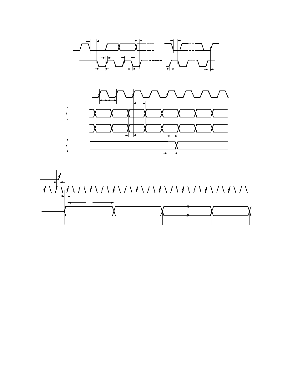
5 V TIMING SPECIFICATIONS
(V
AA
= 4.75 V 5.25 V
1
, V
REF
= 1.235 V R
SET
= 150
. All specifications T
MIN
to T
MAX
2
unless
otherwise noted.)
Parameter
Conditions
Min
Typ
Max
Units
MPU PORT
3, 4
SCLOCK Frequency
0
100
kHz
SCLOCK High Pulsewidth, t
1
4.0
µ
s
SCLOCK Low Pulsewidth, t
2
4.7
µ
s
Hold Time (Start Condition), t
3
After This Period the First Clock Is Generated
4.0
µ
s
Setup Time (Start Condition), t
4
Relevant for Repeated Start Condition
4.7
µ
s
Data Setup Time, t
5
250
ns
SDATA, SCLOCK Rise Time, t
6
1
µ
s
SDATA, SCLOCK Fall Time, t
7
300
ns
Setup Time (Stop Condition), t
8
4.7
µ
s
ANALOG OUTPUTS
3, 5
Analog Output Delay
5
ns
DAC Analog Output Skew
0
ns
CLOCK CONTROL
AND PIXEL PORT
3, 6
F
CLOCK
27
MHz
Clock High Time, t
9
8
ns
Clock Low Time, t
10
8
ns
Data Setup Time, t
11
3.5
ns
Data Hold Time, t
12
4
ns
Control Setup Time, t
11
4
ns
Control Hold Time, t
12
3
ns
Digital Output Access Time, t
13
24
ns
Digital Output Hold Time, t
14
4
ns
Pipeline Delay, t
15
37
Clock Cycles
TELETEXT PORT
3, 7
Digital Output Access Time, t
16
20
ns
Data Setup Time, t
17
1
ns
Data Hold Time, t
18
2
ns
RESET CONTROL
3, 4
RESET Low Time
6
ns
NOTES
1
The max/min specifications are guaranteed over this range.
2
Temperature range T
MIN
to T
MAX
: 0
o
C to +70
o
C.
3
TTL input values are 0 to 3 volts, with input rise/fall times
3 ns, measured between the 10% and 90% points. Timing reference points at 50% for inputs and
outputs. Analog output load
10 pF.
4
Guaranteed by characterization.
5
Output delay measured from the 50% point of the rising edge of CLOCK to the 50% point of full-scale transition.
6
Pixel Port consists of the following:
Pixel Inputs:
P15P0
Pixel Controls:
HSYNC, FIELD/VSYNC, BLANK
Clock Input:
CLOCK
7
Teletext Port consists of the following:
Teletext Output:
TTXREQ
Teletext Input:
TTX
Specifications subject to change without notice.

7
REV. B
ADV7175A/ADV7176A
3.3 V TIMING SPECIFICATIONS
(V
AA
= 3.0 3.6
1
, V
REF
= 1.235 V R
SET
= 300
. All specifications T
MIN
to T
MAX
2
unless
otherwise noted.)
Parameter
Conditions
Min
Typ
Max
Units
MPU PORT
3, 4
SCLOCK Frequency
0
100
kHz
SCLOCK High Pulsewidth, t
1
4.0
µ
s
SCLOCK Low Pulsewidth, t
2
4.7
µ
s
Hold Time (Start Condition), t
3
After This Period the First Clock Is Generated
4.0
µ
s
Setup Time (Start Condition), t
4
for Repeated Start Condition
4.7
µ
s
Data Setup Time, t
5
250
ns
SDATA, SCLOCK Rise Time, t
6
1
µ
s
SDATA, SCLOCK Fall Time, t
7
300
ns
Setup Time (Stop Condition), t
8
4.7
µ
s
ANALOG OUTPUTS
3, 5
Analog Output Delay
7
ns
DAC Analog Output Skew
0
ns
CLOCK CONTROL
AND PIXEL PORT
3, 4, 6, 7
F
CLOCK
27
MHz
Clock High Time, t
9
8
ns
Clock Low Time, t
10
8
ns
Data Setup Time, t
11
3.5
ns
Data Hold Time, t
12
4
ns
Control Setup Time, t
11
4
ns
Control Hold Time, t
12
3
ns
Digital Output Access Time, t
13
24
ns
Digital Output Hold Time, t
14
4
ns
Pipeline Delay, t
15
37
Clock Cycles
TELETEXT PORT
3, 6, 8
Digital Output Access Time t
16
23
ns
Data Setup Time, t
17
2
ns
Data Hold Time, t
18
2
ns
RESET CONTROL
3, 4
RESET Low Time
6
ns
NOTES
1
The max/min specifications are guaranteed over this range.
2
Temperature range T
MIN
to T
MAX
: 0
o
C to +70
o
C.
3
TTL input values are 0 to 3 volts, with input rise/fall times
3 ns, measured between the 10% and 90% points. Timing reference points at 50% for inputs and
outputs. Analog output load
10 pF.
4
Guaranteed by characterization.
5
Output delay measured from the 50% point of the rising edge of CLOCK to the 50% point of full-scale transition.
6
Characterized by design.
7
Pixel Port consists of the following:
Pixel Inputs:
P15P0
Pixel Controls:
HSYNC, FIELD/VSYNC, BLANK
Clock Input:
CLOCK
8
Teletext Port consists of the following:
Teletext Output:
TTXREQ
Teletext Input:
TTX
Specifications subject to change without notice.
ADV7175A/ADV7176A
8
REV. B
t
3
t
2
t
6
t
1
t
7
t
5
t
3
t
4
t
8
SDATA
SCLOCK
Figure 1. MPU Port Timing Diagram
t
9
t
11
CLOCK
PIXEL INPUT
DATA
t
10
t
12
HSYNC
,
FIELD/
VSYNC
,
BLANK
Cb
Y
Cr
Y
Cb
Y
HSYNC
,
FIELD/
VSYNC
,
BLANK
t
13
t
14
CONTROL
I/PS
CONTROL
O/PS
Figure 2. Pixel and Control Data Timing Diagram
TXT
CLOCK
TXTREQ
t
16
4 CLOCK
CYCLES
3 CLOCK
CYCLES
t
17
t
18
4 CLOCK
CYCLES
4 CLOCK
CYCLES
Figure 3. Teletext Timing Diagram
ADV7175A/ADV7176A
9
REV. B
ABSOLUTE MAXIMUM RATINGS
1
V
AA
to GND . . . . . . . . . . . . . . . . . . . . . . . . . . . . . . . . . . . 7 V
Voltage on Any Digital Input Pin . GND 0.5 V to V
AA
+ 0.5 V
Storage Temperature (T
S
) . . . . . . . . . . . . . . 65
°
C to +150
°
C
Junction Temperature (T
J
) . . . . . . . . . . . . . . . . . . . . . +150
°
C
Lead Temperature (Soldering, 10 secs) . . . . . . . . . . . +260
°
C
Analog Outputs to GND
2
. . . . . . . . . . . . . GND 0.5 to V
AA
NOTES
1
Stresses above those listed under Absolute Maximum Ratings may cause permanent
damage to the device. This is a stress rating only; functional operation of the device
at these or any other conditions above those listed in the operational sections of this
specification is not implied. Exposure to absolute maximum rating conditions for
extended periods may affect device reliability.
2
Analog output short circuit to any power supply or common can be of an indefinite
duration.
ORDERING GUIDE
Temperature Package
Package
Model
Range
Description
Option
ADV7175AKS 0
°
C to +70
°
C
Plastic Quad Flatpack S-44
ADV7176AKS 0
°
C to +70
°
C
Plastic Quad Flatpack S-44
CAUTION
ESD (electrostatic discharge) sensitive device. Electrostatic charges as high as 4000 V readily
accumulate on the human body and test equipment and can discharge without detection.
Although the ADV7175A/ADV7176A feature proprietary ESD protection circuitry, permanent
damage may occur on devices subjected to high energy electrostatic discharges. Therefore, pr oper
ESD precautions are recommended to avoid performance degradation or loss of functionality.
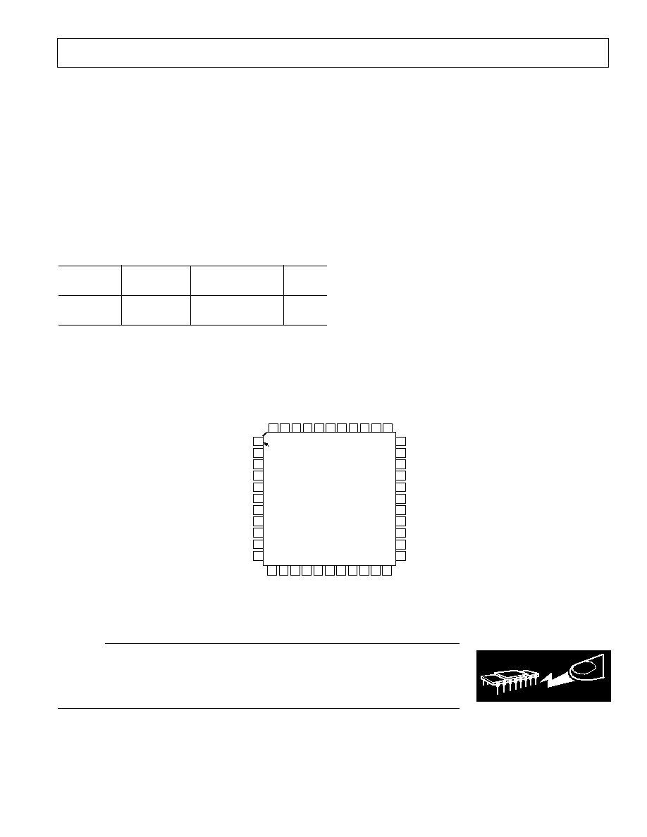
PIN CONFIGURATION
WARNING!
ESD SENSITIVE DEVICE
12 13 14 15 16 17 18 19 20 21 22
3
4
5
6
7
1
2
10
11
8
9
40 39 38
41
42
43
44
36 35 34
37
29
30
31
32
27
28
25
26
23
24
33
PIN 1
IDENTIFIER
V
REF
DAC A
DAC B
V
AA
GND
V
AA
DAC D
BLANK
P13
P14
P15
HSYNC
FIELD/
VSYNC
ALSB
V
AA
P5
P6
P7
P8
P9
P10
P11
P12
GND
V
AA
DAC C
COMP
SDATA
SCLOCK
GND
V
AA
GND
RESET
CLOCK
GND
P4
P3
P2
P1
P0
TTX/V
AA
TTXREQ/GND
SCRESET
/
RTC
R
SET
ADV7175A/ADV7176A
PQFP
TOP VIEW
(Not to Scale)
PACKAGE THERMAL PERFORMANCE
The 44-PQFP package used for this device takes advantage of
an ADI patented thermal coastline lead frame construction.
This maximizes heat transfer into the leads and reduces the
package thermal resistance.
The junction-to-ambient (
JA
) thermal resistance in still air on a
four-layer PCB is 35.5
°
C/W. The junction-to-case thermal
resistance (
JC
) is 13.75
°
C/W.

ADV7175A/ADV7176A
10
REV. B
PIN FUNCTION DESCRIPTIONS
Pin
Input/
No.
Mnemonic
Output
Function
1, 11, 20,
28, 30
V
AA
P
Power Supply (+3 V to +5 V).
10, 19, 21,
29, 43
GND
G
Ground Pin.
15
HSYNC
I/O
HSYNC (Modes 1 and 2) Control Signal. This pin may be configured to
output (Master Mode) or accept (Slave Mode) Sync signals.
16
FIELD/
VSYNC
I/O
Dual Function FIELD (Mode 1) and
VSYNC (Mode 2) Control Signal. This
pin may be configured to output (Master Mode) or accept (Slave Mode)
these control signals.
17
BLANK
I/O
Video Blanking Control Signal. The pixel inputs are ignored when this is
logic level "0." This signal is optional.
18
ALSB
I
TTL Address Input. This signal sets up the LSB of the MPU address.
22
RESET
I
The input resets the on chip timing generator and sets the ADV7175A/
ADV7176A into default mode. This is NTSC operation, Timing Slave Mode
0, 8-bit operation, 2
×
composite and S-Video out and all DACs powered on.
23
SCLOCK
I
MPU Port Serial Interface Clock Input.
24
SDATA
I/O
MPU Port Serial Data Input/Output.
25
COMP
O
Compensation Pin. Connect a 0.1
µ
F capacitor from COMP to V
AA
. For
Optimum Dynamic Performance in Low Power Mode, the value of the
COMP capacitor can be lowered to as low as 2.2 nF.
26
DAC C
O
RED/S-Video C/V Analog Output.
27
DAC D
O
GREEN/S-Video Y/Y Analog Output.
31
DAC B
O
BLUE/Composite/U Analog Output.
32
DAC A
O
PAL/NTSC Composite Video Output. Full-Scale Output is 180IRE (1286
mV) for NTSC and 1300 mV for PAL.
33
V
REF
I/O
Voltage Reference Input for DACs or Voltage Reference Output (1.235 V).
34
R
SET
I
A 150
resistor connected from this pin to GND is used to control full-scale
amplitudes of the video signals.
35
SCRESET/RTC
I
This pin can be configured as an input by setting MR22 and MR21 of Mode
Register 2. It can be configured as a subcarrier reset pin, in which case a high
to low transition on this pin will reset the subcarrier to Field 0. Alternatively
it may be configured as a Real Time Control (RTC) input.
36
TTXREQ/GND
O
Teletext Data Request Signal/Defaults to GND when Teletext not selected
(enables backward compatibility to ADV7175/ADV7176).
37
TTX/V
AA
I
Teletext Data/Defaults to V
AA
when Teletext not selected (enables backward
compatibility to ADV7175/ADV7176).
3842
P0P15
I
8-Bit 4:2:2 Multiplexed YCrCb Pixel Port (P7P0) or
29, 1214
16-Bit YCrCb Pixel Port (P0P15). P0 represents the LSB.
44
CLOCK
I
TTL Clock Input. Requires a stable 27 MHz reference Clock for standard
operation. Alternatively, a 24.52 MHz (NTSC) or 29.5 MHz (PAL) can be
used for square pixel operation.

ADV7175A/ADV7176A
11
REV. B
signal compatible with worldwide standards. The 4:2:2 YUV
video data is interpolated to two times the pixel rate. The
color-difference components (UV) are quadrature modulated
using a subcarrier frequency generated by an on-chip 32-bit
digital synthesizer (also running at two times the pixel rate).
The two times pixel rate sampling allows for better signal-to-
noise-ratio. A 32-bit DDS with a 10-bit look-up table produces
a superior subcarrier in terms of both frequency and phase. In
addition to the composite output signal, there is the facility to
output S-Video (Y/C) video, YUV or RGB video. The Y/C,
YUV or RGB format is simultaneously available at the analog
outputs with the composite video signal.
Each analog output is capable of driving the full video-level
(35 mA) signal into an unbuffered, doubly terminated 75
load. With external buffering, the user has the additional option
to scale back the DAC output current to 5 mA min, thereby signifi-
cantly reducing the power dissipation of the device.
The ADV7175A/ADV7176A also supports both PAL and NTSC
square pixel operation.
The output video frames are synchronized with the incoming
data timing reference codes. Optionally the encoder accepts
(and can generate)
HSYNC, VSYNC and FIELD timing signals.
These timing signals can be adjusted to change pulsewidth and
position while the part is in the master mode. The encoder
requires a single two times pixel rate (27 MHz) clock for standard
operation. Alternatively, the encoder requires a 24.54 MHz clock
for NTSC or 29.5 MHz clock for PAL square pixel mode
operation. All internal timing is generated on-chip.
A separate teletext port enables the user to directly input teletext
data during the vertical blanking interval.
The ADV7175A/ADV7176A modes are set up over a two-wire
serial bidirectional port (I
2
C Compatible) with two slave addresses.
Functionally the ADV7175A and ADV7176A are the same with
the exception that the ADV7175A can output the Macrovision
anticopy algorithm.
The ADV7175A/ADV7176A is packaged in a 44-lead thermally
enhanced PQFP package.
DATA PATH DESCRIPTION
For PAL B, D, G, H, I, M, N and NTSC M modes, YCrCb
4:2:2 data is input via the CCIR-656 compatible pixel port at a
27 MHz Data Rate. The pixel data is demultiplexed to from
three data paths. Y typically has a range of 16 to 235, Cr and
Cb typically have a range of 128
±
112; however, it is possible
to input data from 1 to 254 on both Y, Cb and Cr. The
ADV7175A/ADV7176A supports PAL (B, D, G, H, I, N, M)
and NTSC (with and without Pedestal) standards. The ap-
propriate SYNC, BLANK and Burst levels are added to the
YCrCb data. Macrovision antitaping (ADV7175A only),
closed captioning and teletext levels are also added to Y, and
the resultant data is interpolated to a rate of 27 MHz. The
interpolated data is filtered and scaled by three digital FIR
filters.
The U and V signals are modulated by the appropriate subcarrier
sine/cosine phases and added together to make up the chromi-
nance signal. The luma (Y) signal can be delayed 13 luma
cycles (each cycle is 74 ns) with respect to the chroma signal.
The luma and chroma signals are then added together to make
up the composite video signal. All edges are slew rate limited.
The YCrCb data is also used to generate RGB data with
appropriate SYNC and BLANK levels. The RGB data is in
synchronization with the composite video output. Alternatively
analog YUV data can be generated instead of RGB.
The four 10-bit DACs can be used to output:
1. Composite Video + RGB Video.
2. Composite Video + YUV Video
3. Two Composite Video Signals + LUMA and CHROMA
3.
(Y/C) Signals.
Alternatively, each DAC can be individually powered off if not
required.
Video output levels are illustrated in Appendix 4 and Appendix 5.
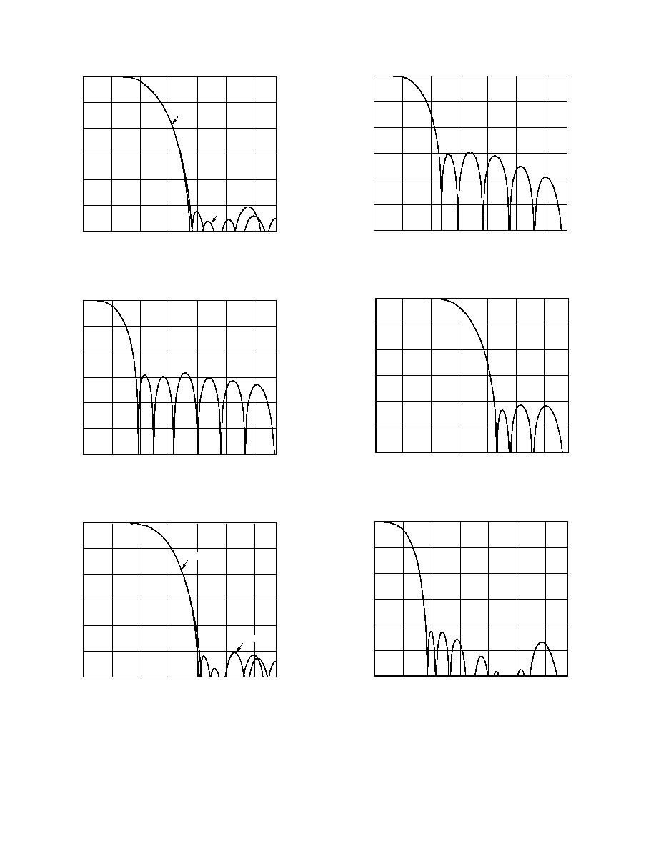
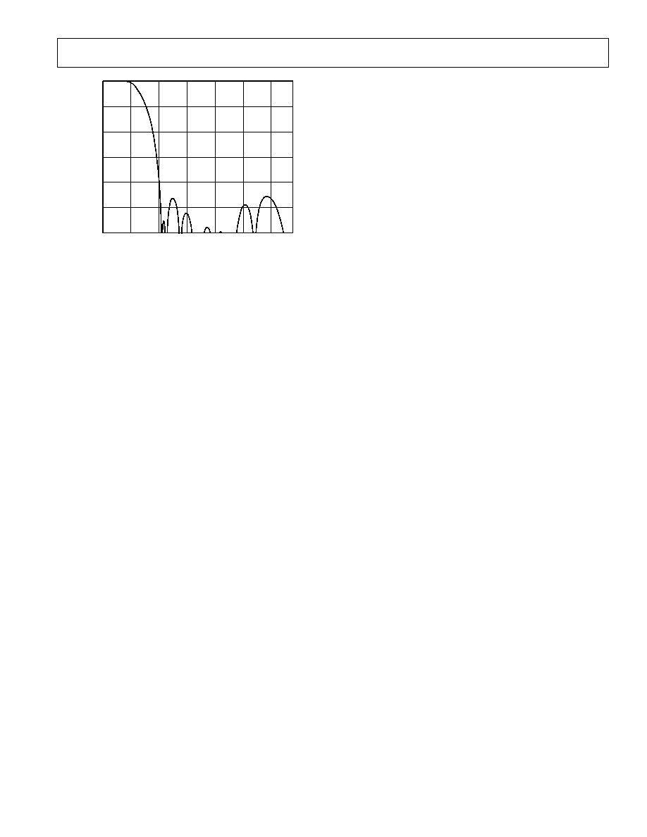
INTERNAL FILTER RESPONSE
The Y filter supports several different frequency responses,
including two 4.5 MHz/5.0 MHz low pass responses, PAL/
NTSC subcarrier notch responses and a PAL/NTSC extended
response. The U and V filters have a 2/2.4 MHz low-pass
response for NTSC/PAL. These filter characteristics are illus-
trated in Figures 4 to 12.
MR04
MR03
NTSC
0
0
2.3
0.026
7.0
>
54
4.2
PAL
0
0
3.4
0.098
7.3
>
50
5.0
NTSC
0
1
1.0
0.085
3.57
>
27.6
2.1
PAL
0
1
1.4
0.107
4.43
>
29.3
2.7
NTSC/PAL
1 0
4.0
0.150
7.5
>
40
5.65
NTSC
1
1
2.3
0.054
7.0
>
54
4.2
PAL
1
1
3.4
0.106
7.3
>
50.3
5.0
FILTER SELECTION
F
3dB
PASSBAND
CUTOFF (MHz)
STOPBAND
CUTOFF (MHz)
PASSBAND
RIPPLE (dB)
STOPBAND
ATTENUATION (dB)
Figure 4. Luminance Internal Filter Specifications
NTSC
1.0
0.085
3.2
>
40
0.3
2.05
PAL
1.3
0.04
4.0
>
40
0.02
2.45
FILTER SELECTION
F
3dB
PASSBAND
CUTOFF (MHz)
STOPBAND
CUTOFF (MHz)
PASSBAND
RIPPLE (dB)
STOPBAND
ATTENUATION (dB)
ATTENUATION @
1.3MHz (dB)
Figure 5. Chrominance Internal Filter Specifications
(Continued from page 1)
ADV7175A/ADV7176A
12
REV. B
TYPE A
TYPE B
FREQUENCY MHz
0
60
50
40
10
20
30
0
2
4
6
8
12
10
AMPLITUDE dB
Figure 6. NTSC Low-Pass Filter
FREQUENCY MHz
0
60
50
40
10
20
30
0
2
4
6
8
12
10
AMPLITUDE dB
Figure 7. NTSC Notch Filter
FREQUENCY MHz
0
60
50
40
10
20
30
0
2
4
6
8
12
10
AMPLITUDE dB
TYPE A
TYPE B
Figure 8. PAL Low-Pass Filter
FREQUENCY MHz
0
60
50
40
10
20
30
0
2
4
6
8
12
10
AMPLITUDE dB
Figure 9. PAL Notch Filter
FREQUENCY MHz
60
50
40
10
20
30
0
2
4
6
8
12
10
AMPLITUDE dB
Figure 10. NTSC/PAL Extended Mode Filter
FREQUENCY MHz
0
60
50
40
10
20
30
0
2
4
6
8
12
10
AMPLITUDE dB
Figure 11. NTSC UV Filter
ADV7175A/ADV7176A
13
REV. B
COLOR BAR GENERATION
The ADV7175A/ADV7176A can be configured to generate
75% amplitude, 75% saturation (75/7.5/75/7.5) for NTSC or
75% amplitude, 100% saturation (100/0/75/0) for PAL color
bars. These are enabled by setting MR17 of Mode Register 1 to
Logic "1."
SQUARE PIXEL MODE
The ADV7175A/ADV7176A can be used to operate in square
pixel mode. For NTSC operation an input clock of 24.5454
MHz is required. Alternatively an input clock of 29.5 MHz is
required for PAL operation. The internal timing logic adjusts
accordingly for square pixel mode operation.
COLOR SIGNAL CONTROL
The color information can be switched on and off the video
output using Bit MR24 of Mode Register 2.
BURST SIGNAL CONTROL
The burst information can be switched on and off the video
output using Bit MR25 of Mode Register 2.
NTSC PEDESTAL CONTROL
The pedestal on both odd and even fields can be controlled on a
line by line basis using the NTSC Pedestal Control Registers.
This allows the pedestals to be controlled during the vertical
blanking interval (Lines 10 to 25 and Lines 273 to 288).
PIXEL TIMING DESCRIPTION
The ADV7175A/ADV7176A can operate in either 8-bit or
16-bit YCrCb Mode.
8-Bit YCrCb Mode
This default mode accepts multiplexed YCrCb inputs through
the P7-P0 pixel inputs. The inputs follow the sequence Cb0, Y0
Cr0, Y1 Cb1, Y2, etc. The Y, Cb and Cr data are input on a
rising clock edge.
16-Bit YCrCb Mode
This mode accepts Y inputs through the P7P0 pixel inputs and
multiplexed CrCb inputs through the P15P8 pixel inputs. The
data is loaded on every second rising edge of CLOCK. The inputs
follow the sequence Cb0, Y0 Cr0, Y1 Cb1, Y2, etc.
SUBCARRIER RESET
Together with the SCRESET/RTC PIN and Bits MR22 and
MR21 of Mode Register 2, the ADV7175A/ADV7176A can be
used in subcarrier reset mode. The subcarrier will reset to
Field 0 at the start of the following field when a low to high
transition occurs on this input pin.
REAL TIME CONTROL
Together with the SCRESET/RTC PIN and Bits MR22 and
MR21 of Mode Register 2, the ADV7175A/ADV7176A can be
used to lock to an external video source. The real time control
mode allows the ADV7175A/ADV7176A to automatically alter
the subcarrier frequency to compensate for line length variation.
When the part is connected to a device that outputs a digital
datastream in the RTC format (such as an ADV7185 video
decoder [see Figure 13]), the part will automatically change to
the compensated subcarrier frequency on a line by line basis.
This digital datastream is 67 bits wide and the subcarrier is
contained in Bits 0 to 21. Each bit is two clock cycles long.
00HEX should be written to all four subcarrier frequency regis-
ters when using this mode.
VIDEO TIMING DESCRIPTION
The ADV7175A/ADV7176A is intended to interface to off-
the-shelf MPEG1 and MPEG2 Decoders. Consequently, the
ADV7175A/ADV7176A accepts 4:2:2 YCrCb Pixel Data via a
CCIR-656 pixel port and has several video timing modes of
operation that allow it to be configured as either system master
video timing generator or a slave to the system video timing
generator. The ADV7175A/ADV7176A generates all of the
required horizontal and vertical timing periods and levels for the
analog video outputs.
The ADV7175A/ADV7176A calculates the width and place-
ment of analog sync pulses, blanking levels and color burst
envelopes. Color bursts are disabled on appropriate lines, and
serration and equalization pulses are inserted where required.
In addition the ADV7175A/ADV7176A supports a PAL or
NTSC square pixel operation in slave mode. The part requires
an input pixel clock of 24.5454 MHz for NTSC and an input
pixel clock of 29.5 MHz for PAL. The internal horizontal line
counters place the various video waveform sections in the cor-
rect location for the new clock frequencies.
The ADV7175A/ADV7176A has four distinct master and four
distinct slave timing configurations. Timing Control is estab-
lished with the bidirectional
SYNC, BLANK and FIELD/
VSYNC pins. Timing Mode Register 1 can also be used to vary
the timing pulsewidths and where they occur in relation to each
other.
FREQUENCY MHz
0
60
50
40
10
20
30
0
2
4
6
8
12
10
AMPLITUDE dB
Figure 12. PAL UV Filter
ADV7175A/ADV7176A
14
REV. B
COMPOSITE
VIDEO
e.g., VCR
OR CABLE
M
U
X
HSYNC
FIELD/
VSYNC
CLOCK
GREEN/LUMA/Y
RED/CHROMA/V
BLUE/COMPOSITE/U
COMPOSITE
ADV7175A/ADV7176A
P7P0
SCRESET/RTC
MPEG
DECODER
VIDEO
DECODER
(e.g., ADV7185)
H/LTRANSITION
COUNT START
LOW
128
RTC
TIME SLOT: 01
14
67 68
NOT USED IN
ADV7175A/ADV7176A
19
VALID
SAMPLE
INVALID
SAMPLE
FSCPLL INCREMENT
1
8/LLC
5 BITS
RESERVED
SEQUENCE
BIT
2
RESET
BIT
3
RESERVED
4 BITS
RESERVED
21
0
13
14 BITS
RESERVED
NOTES:
1
F
SC
PLL INCREMENT IS 22 BITS LONG, VALUED LOADED INTO ADV7175A/ADV7176A FSC DDS REGISTER IS
F
SC
PLL INCREMENTS BITS 21:0 PLUS BITS 0:9 OF SUB CARRIER FREQUENCY REGISTERS. ALL ZEROS SHOULD
BE WRITTEN TO THE SUB CARRIER FREQUENCY REGISTERS OF THE ADV7175A/ADV7176A.
2
SEQUENCE BIT
PAL: 0 = LINE NORMAL, 1 = LINE INVERTED
NTSC: 0 = NO CHANGE.
3
RESET BIT
RESET ADV7175A/ADV7176A's DDS.
0
Figure 13. RTC Timing and Connections
Vertical Blanking Data Insertion
It is possible to allow encoding of incoming YCbCr data on those lines of VBI that do not bear line sync or pre/post-equalization
pulses (see Figures 15 to 26). This mode of operation is called "Partial Blanking" and is selected by setting MR31 to 1. It allows the
insertion of any VBI data (Opened VBI) into the encoded output waveform. This data is present in digitized incoming YCbCr data
stream (e.g., WSS data, CGMS, VPS, etc.). Alternatively, the entire VBI may be blanked (no VBI data inserted) on these lines by
setting MR31 to 0.
The complete VBI comprises of the following lines:
525/60 Systems, Lines 525 to 21 for Field 1 and Lines 262 to Line 284 for Field 2.
625/50 Systems, Lines 624 to Line 22 and Lines 311 to 335.
The "Opened VBI" consists of:
525/60 Systems, Lines 10 to 21 for Field 1 and second half of Line 273 to Line 284 for Field 2.
625/50 Systems, Line 7 to Line 22 and Lines 319 to 335.
Mode 0 (CCIR-656): Slave Option
(Timing Register 0 TR0 = X X X X X 0 0 0)
The ADV7175A/ADV7176A is controlled by the SAV (Start Active Video) and EAV (End Active Video) time codes in the pixel
data. All timing information is transmitted using a 4-byte synchronization pattern. A synchronization pattern is sent immediately
before and after each line during active picture and retrace. Mode 0 is illustrated in Figure 14. The
HSYNC, FIELD/VSYNC and
BLANK (if not used) pins should be tied high during this mode.
ADV7175A/ADV7176A
15
REV. B
Y
C
r
Y
F
F
0
0
0
0
X
Y
8
0
1
0
8
0
1
0
F
F
0
0
F
F
A
B
A
B
A
B
8
0
1
0
8
0
1
0
F
F
0
0
0
0
X
Y
C
b
Y C
r
C
b
Y
C
b
Y
C
r
EAV CODE
SAV CODE
ANCILLARY DATA
(HANC)
4 CLOCK
4 CLOCK
268 CLOCK
1440 CLOCK
4 CLOCK
4 CLOCK
280 CLOCK
1440 CLCOK
END OF ACTIVE
VIDEO LINE
START OF ACTIVE
VIDEO LINE
ANALOG
VIDEO
INPUT PIXELS
NTSC/PAL M SYSTEM
(525 LlNES/60Hz)
PAL SYSTEM
(625 LINES/50Hz)
Y
Figure 14. Timing Mode 0 (Slave Mode)
Mode 0 (CCIR-656): Master Option
(Timing Register 0 TR0 = X X X X X 0 0 1)
The ADV7175A/ADV7176A generates H, V and F signals required for the SAV (Start Active Video) and EAV (End Active Video)
time codes in the CCIR-656 standard. The H bit is output on the
HSYNC pin, the V bit is output on the BLANK pin, and the F bit
is output on the FIELD/
VSYNC pin. Mode 0 is illustrated in Figure 15 (NTSC) and Figure 16 (PAL). The H, V and F transitions
relative to the video waveform are illustrated in Figure 17.
522
523
524
525
1
2
3
4
5
6
7
8
9
10
11
20
21
22
DISPLAY
DISPLAY
VERTICAL BLANK
ODD FIELD
EVEN FIELD
H
V
F
260
261
262
263
264
265
266
267
268
269
270
271
272
273
274
283
284
285
ODD FIELD
EVEN FIELD
DISPLAY
DISPLAY
VERTICAL BLANK
H
V
F
Figure 15. Timing Mode 0 (NTSC Master Mode)
ADV7175A/ADV7176A
16
REV. B
622
623
624
625
1
2
3
4
5
6
7
21
22
23
DISPLAY
DISPLAY
VERTICAL BLANK
H
V
F
ODD FIELD
EVEN FIELD
309
310
311
312
314
315
316
317
318
319
320
334
335
336
DISPLAY
DISPLAY
VERTICAL BLANK
H
V
F
ODD FIELD
EVEN FIELD
313
Figure 16. Timing Mode 0 (PAL Master Mode)
ANALOG
VIDEO
H
F
V
Figure 17. Timing Mode 0 Data Transitions (Master Mode)
Mode 1: Slave Option
HSYNC, BLANK, FIELD
(Timing Register 0 TR0 = X X X X X 0 1 0)
In this mode the ADV7175A/ADV7176A accepts horizontal SYNC and Odd/Even FIELD signals. A transition of the FIELD input
when
HSYNC is low indicates a new frame i.e., vertical retrace. The BLANK signal is optional. When the BLANK input is disabled
the ADV7175A/ADV7176A automatically blanks all normally blank lines. Mode 1 is illustrated in Figure 18 (NTSC) and Fig-
ure 19 (PAL).
ADV7175A/ADV7176A
17
REV. B
260
261
262
263
264
265
266
267
268
269
270
271
272
273
274
283
284
285
ODD FIELD
EVEN FIELD
DISPLAY
DISPLAY
VERTICAL BLANK
HSYNC
BLANK
FIELD
522
523
524
525
1
2
3
4
5
6
7
8
9
10
11
20
21
22
DISPLAY
DISPLAY
VERTICAL BLANK
ODD FIELD
EVEN FIELD
HSYNC
BLANK
FIELD
Figure 18. Timing Mode 1 (NTSC)
622
623
624
625
1
2
3
4
5
6
7
21
22
23
DISPLAY
VERTICAL BLANK
ODD FIELD
EVEN FIELD
HSYNC
BLANK
FIELD
DISPLAY
309
310
311
312
313
314
315
316
317
318
319
334
335
336
DISPLAY
VERTICAL BLANK
ODD FIELD
EVEN FIELD
HSYNC
BLANK
FIELD
DISPLAY
320
Figure 19. Timing Mode 1 (PAL)
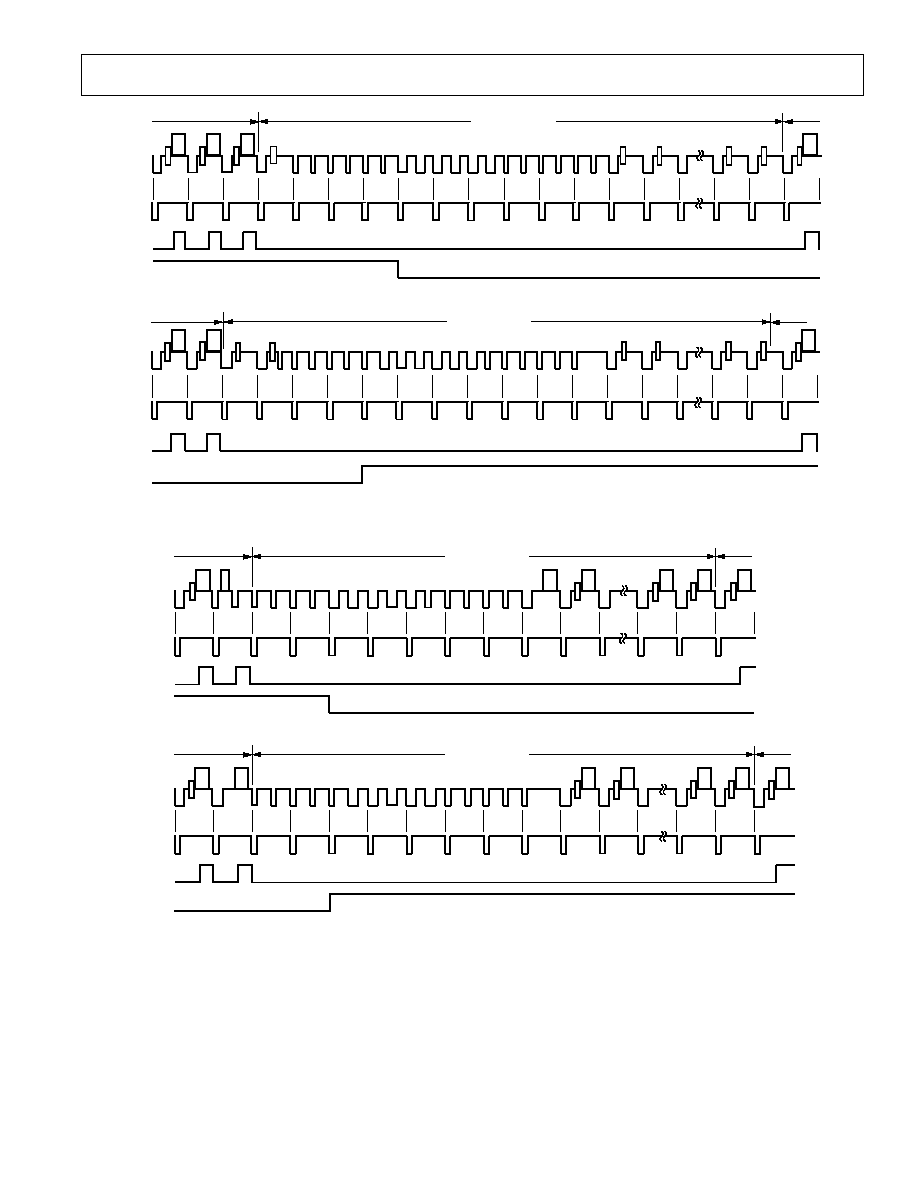
Mode 1: Master Option
HSYNC, BLANK, FIELD
(Timing Register 0 TR0 = X X X X X 0 1 1)
In this mode the ADV7175A/ADV7176A can generate horizontal SYNC and Odd/Even FIELD signals. A transition of the FIELD
input when
HSYNC is low indicates a new frame i.e., vertical retrace. The BLANK signal is optional. When the BLANK input is
disabled, the ADV7175A/ADV7176A automatically blanks all normally blank lines. Pixel data is latched on the rising clock edge
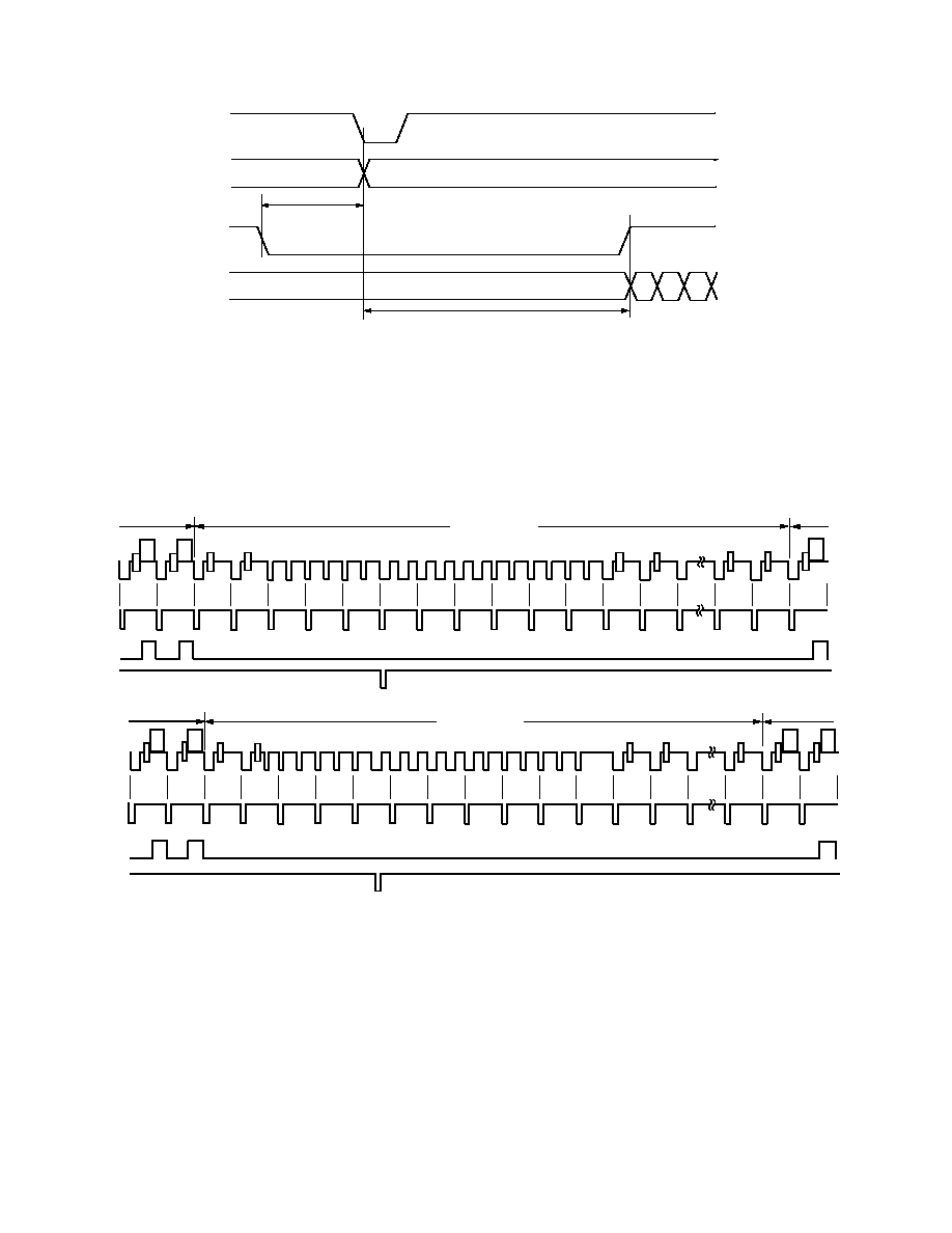
following the timing signal transitions. Mode 1 is illustrated in Figure 18 (NTSC) and Figure 19 (PAL). Figure 20 illustrates the
HSYNC, BLANK and FIELD for an odd or even field transition relative to the pixel data.
ADV7175A/ADV7176A
18
REV. B
FIELD
PIXEL
DATA
PAL = 12 * CLOCK/2
NTSC = 16 * CLOCK/2
PAL = 132 * CLOCK/2
NTSC = 122 * CLOCK/2
Cb
Y
Cr
Y
HSYNC
BLANK
Figure 20. Timing Mode 1 Odd/Even Field Transitions Master/Slave
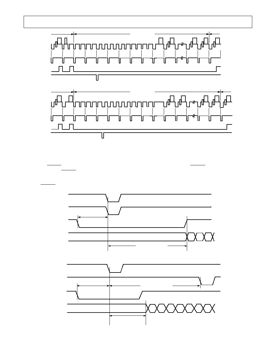
Mode 2: Slave Option
HSYNC, VSYNC, BLANK
(Timing Register 0 TR0 = X X X X X 1 0 0 )
In this mode the ADV7175A/ADV7176A accepts horizontal and vertical SYNC signals. A coincident low transition of both
HSYNC and VSYNC inputs indicates the start of an odd field. A VSYNC low transition when HSYNC is high indicates the start of
an even field. The
BLANK signal is optional. When the BLANK input is disabled, the ADV7175A/ADV7176A automatically blanks
all normally blank lines as per CCIR-624. Mode 2 is illustrated in Figure 21 (NTSC) and Figure 22 (PAL).
522
523
524
525
1
2
3
4
5
6
7
8
9
10
11
20
21
22
DISPLAY
DISPLAY
VERTICAL BLANK
ODD FIELD
EVEN FIELD
HSYNC
BLANK
VSYNC
260
261
262
263
264
265
266
267
268
269
270
271
272
273
274
283
284
285
ODD FIELD
EVEN FIELD
DISPLAY
DISPLAY
VERTICAL BLANK
HSYNC
BLANK
VSYNC
Figure 21. Timing Mode 2 (NTSC)
ADV7175A/ADV7176A
19
REV. B
622
623
624
625
1
2
3
4
5
6
7
21
22
23
DISPLAY
VERTICAL BLANK
ODD FIELD
EVEN FIELD
HSYNC
BLANK
VSYNC
DISPLAY
309
310
311
312
313
314
315
316
317
318
319
334
335
336
DISPLAY
VERTICAL BLANK
ODD FIELD
EVEN FIELD
HSYNC
BLANK
DISPLAY
320
VSYNC
Figure 22. Timing Mode 2 (PAL)
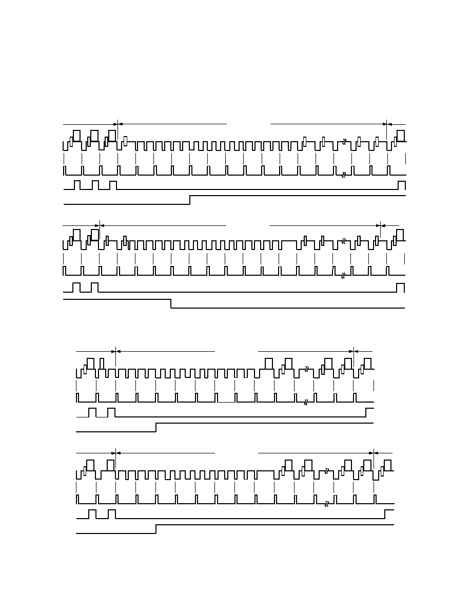
Mode 2: Master Option
HSYNC, VSYNC, BLANK
(Timing Register 0 TR0 = X X X X X 1 0 1)
In this mode, the ADV7175A/ADV7176A can generate horizontal and vertical SYNC signals. A coincident low transition of both
HSYNC and VSYNC inputs indicates the start of an Odd Field. A VSYNC low transition when HSYNC is high indicates the start
of an even field. The
BLANK signal is optional. When the BLANK input is disabled, the ADV7175A/ADV7176A automatically
blanks all normally blank lines as per CCIR-624. Mode 2 is illustrated in Figure 21 (NTSC) and Figure 22 (PAL). Figure 23
illustrates the
HSYNC, BLANK and VSYNC for an even-to-odd field transition relative to the pixel data. Figure 24 illustrates the
HSYNC, BLANK and VSYNC for an odd-to-even field transition relative to the pixel data.
PAL = 12 * CLOCK/2
NTSC = 16 * CLOCK/2
HSYNC
VSYNC
BLANK
PIXEL
DATA
PAL = 132 * CLOCK/2
NTSC = 122 * CLOCK/2
Cb
Y
Cr
Y
Figure 23. Timing Mode 2 Even-to-Odd Field Transition Master/Slave
PAL = 864 * CLOCK/2
NTSC = 858 * CLOCK/2
PAL = 132 * CLOCK/2
NTSC = 122 * CLOCK/2
HSYNC
VSYNC
BLANK
PIXEL
DATA
PAL = 12 * CLOCK/2
NTSC = 16 * CLOCK/2
Cb
Y
Cr
Y
Cb
Figure 24. Timing Mode 2 Odd-to-Even Field Transition Master/Slave
ADV7175A/ADV7176A
20
REV. B
Mode 3: Master/Slave Option
HSYNC, BLANK, FIELD
(Timing Register 0 TR0 = X X X X X 1 1 0 or X X X X X 1 1 1)
In this mode, the ADV7175A/ADV7176A accepts or generates Horizontal SYNC and Odd/Even FIELD signals. A transition of the
FIELD input when
HSYNC is high indicates a new frame i.e., vertical retrace. The BLANK signal is optional. When the BLANK
input is disabled, the ADV7175A/ADV7176A automatically blanks all normally blank lines as per CCIR-624. Mode 3 is illustrated
in Figure 25 (NTSC) and Figure 26 (PAL).
260
261
262
263
264
265
266
267
268
269
270
271
272
273
274
283
284
285
ODD FIELD
EVEN FIELD
DISPLAY
DISPLAY
VERTICAL BLANK
HSYNC
BLANK
FIELD
522
523
524
525
1
2
3
4
5
6
7
8
9
10
11
20
21
22
DISPLAY
DISPLAY
VERTICAL BLANK
ODD FIELD
EVEN FIELD
HSYNC
BLANK
FIELD
Figure 25. Timing Mode 3 (NTSC)
622
623
624
625
1
2
3
4
5
6
7
21
22
23
DISPLAY
VERTICAL BLANK
ODD FIELD
EVEN FIELD
HSYNC
BLANK
FIELD
DISPLAY
309
310
311
312
313
314
315
316
317
318
319
334
335
336
DISPLAY
VERTICAL BLANK
ODD FIELD
EVEN FIELD
HSYNC
BLANK
FIELD
DISPLAY
320
Figure 26. Timing Mode 3 (PAL)
ADV7175A/ADV7176A
21
REV. B
OUTPUT VIDEO TIMING
The video timing generator generates the appropriate SYNC,
BLANK and BURST sequence that controls the output analog
waveforms. These sequences are summarized below. In slave
modes, the following sequences are synchronized with the input
timing control signals. In master modes, the timing generator
free runs and generates the following sequences in addition to
the output timing control signals.
NTSCInterlaced: Scan Lines 19 and 264272 are always
blanked and vertical sync pulses are included. Scan Lines 525,
1021 and 262, 263, 273284 are also blanked and can be used
for closed captioning data. Burst is disabled on lines 16, 261
269 and 523525.
NTSCNoninterlaced: Scan Lines 19 are always blanked,
and vertical sync pulses are included. Scan Lines 1021 are also
blanked and can be used for closed captioning data. Burst is
disabled on Lines 16, 261262.
PALInterlaced: Scan Lines 16, 311318 and 624625 are
always blanked, and vertical sync pulses are included in Fields
1, 2, 5 and 6. Scan Lines 15, 311319 and 624625 are al-
ways blanked, and vertical sync pulses are included in Fields 3,
4, 7 and 8. The remaining scan lines in the vertical blanking
interval are also blanked and can be used for teletext data.
Burst is disabled on Lines 16, 311318 and 623625 in Fields
1, 2, 5 and 6. Burst is disabled on Lines 15, 311319 and
623625 in Fields 3, 4, 7 and 8.
PALNoninterlaced: Scan Lines 16 and 311312 are always
blanked, and vertical sync pulses are included. The remaining
scan lines in the vertical blanking interval are also blanked and
can be used for teletext data. Burst is disabled on Lines 15,
310312.
POWER-ON RESET
After power-up, it is necessary to execute a reset operation. A
reset occurs on the falling edge of a high-to-low transition on
the
RESET pin. This initializes the pixel port so that the
pixel inputs, P7P0 are selected. After reset, the ADV7175A/
ADV7176A is automatically set up to operate in NTSC mode.
Subcarrier frequency code 21F07C16HEX is loaded into the
subcarrier frequency registers. All other registers, with the
exception of Mode Register 0, are set to 00H. All bits in Mode
Register 0 are set to Logic Level "0" except Bit MR02. Bit
MR02 of Mode Register 0 is set to Logic "1." This enables the
7.5 IRE pedestal.
SCH Phase Mode
The SCH phase is configured in default mode to reset every
four (NTSC) or eight (PAL) fields to avoid an accumulation of
SCH phase error over time. In an ideal system, zero SCH phase
error would be maintained forever, but in reality, this is impos-
sible to achieve due to clock frequency variations. This effect is
reduced by the use of a 32-bit DDS, which generates this SCH.
Resetting the SCH phase every four or eight fields avoids the
accumulation of SCH phase error, and results in very minor
SCH phase jumps at the start of the four or eight field sequence.
Resetting the SCH phase should not be done if the video source
does not have stable timing or the ADV7175A/ADV7176A is
configured in RTC mode (MR21 = 1 and MR22 = 1). Under
these conditions (unstable video) the subcarrier phase reset
should be enabled MR22 = 0 and MR21 = 1) but no reset
applied. In this configuration the SCH phase will never be reset,
which means that the output video will now track the unstable
input video. The subcarrier phase reset, when applied, will reset
the SCH phase to Field 0 at the start of the next field (e.g.,
subcarrier phase reset applied in Field 5 [PAL] on the start of
the next field SCH phase will be reset to Field 0).
MPU PORT DESCRIPTION
The ADV7175A and ADV7176A support a two-wire serial (I
2
C
Compatible) microprocessor bus driving multiple peripherals.
Two inputs, serial data (SDATA) and serial clock (SCLOCK),
carry information between any device connected to the bus.
Each slave device is recognized by a unique address. The
ADV7175A and ADV7176A each have four possible slave
addresses for both read and write operations. These are unique
addresses for each device and are illustrated in Figure 27 and
Figure 28. The LSB sets either a read or write operation. Logic
Level "1" corresponds to a read operation, while Logic Level
"0" corresponds to a write operation. A1 is set by setting the
ALSB pin of the ADV7175A/ADV7176A to Logic Level "0" or
Logic Level "1."
1
X
1
0
1
0
1
A1
ADDRESS
CONTROL
SET UP BY
ALSB
READ/WRITE
CONTROL
0
WRITE
1
READ
Figure 27. ADV7175A Slave Address
0
X
1
0
1
0
1
A1
ADDRESS
CONTROL
SET UP BY
ALSB
READ/WRITE
CONTROL
0
WRITE
1
READ
Figure 28. ADV7176A Slave Address
To control the various devices on the bus, the following proto-
col must be followed: First, the master initiates a data transfer by
establishing a start condition, defined by a high-to-low transition
on SDATA while SCLOCK remains high. This indicates that
an address/data stream will follow. All peripherals respond to
the start condition and shift the next eight bits (7-bit address +
R/
W bit). The bits transfer from MSB down to LSB. The pe-
ripheral that recognizes the transmitted address responds by
pulling the data line low during the ninth clock pulse. This is
known as an acknowledge bit. All other devices withdraw from
the bus at this point and maintain an idle condition. The idle
condition is where the device monitors the SDATA and SCLOCK
lines waiting for the start condition and the correct transmitted
address. The R/
W bit determines the direction of the data. A
Logic "0" on the LSB of the first byte means that the master
will write information to the peripheral. A Logic "1" on the
LSB of the first byte means that the master will read informa-
tion from the peripheral.
ADV7175A/ADV7176A
22
REV. B
The ADV7175A/ADV7176A acts as a standard slave device on
the bus. The data on the SDATA pin is 8 bits long, supporting
the 7-bit addresses, plus the R/
W bit. The ADV7175A has 33
subaddresses and the ADV7176A has 19 subaddresses to enable
access to the internal registers. It therefore interprets the first
byte as the device address and the second byte as the starting
subaddress. The subaddresses auto increment allow data to
be written to or read from the starting subaddress. A data
transfer is always terminated by a stop condition. The user can
also access any unique subaddress register on a one by one basis
without having to update all the registers. There is one excep-
tion. The subcarrier frequency registers should be updated in
sequence, starting with Subcarrier Frequency Register 0. The
auto increment function should then be used to increment and
access Subcarrier Frequency Registers 1, 2 and 3. The subcarrier
frequency registers should not be accessed independently.
Stop and start conditions can be detected at any stage during
the data transfer. If these conditions are asserted out of sequence
with normal read and write operations, they cause an immediate
jump to the idle condition. During a given SCLOCK high pe-
riod, the user should issue only one start condition, one stop
condition or a single stop condition followed by a single start
condition. If an invalid subaddress is issued by the user, the
ADV7175A/ADV7176A will not issue an acknowledge and will
DATA
A(S)
S
SLAVE ADDR A(S)
SUB ADDR
A(S)
LSB = 0
LSB = 1
DATA
A(S) P
S
SLAVE ADDR A(S)
SUB ADDR
A(S) S
SLAVE ADDR
A(S)
DATA
A(M)
A
(M)
DATA
P
WRITE
SEQUENCE
READ
SEQUENCE
A
(S) = NO-ACKNOWLEDGE BY SLAVE
A
(M) = NO-ACKNOWLEDGE BY MASTER
A(S) = ACKNOWLEDGE BY SLAVE
A(M) = ACKNOWLEDGE BY MASTER
S = START BIT
P = STOP BIT
Figure 30. Write and Read Sequences
SR4
SR3
SR2
SR1
SR0
SR7
SR6
SR5
SR5
SR4 SR3 SR2 SR1 SR0
ADV7175A SUBADDRESS REGISTER
0
0
0
0
0
0
MODE REGISTER 0
0
0
0
0
0
1
MODE REGISTER 1
0
0
0
0
1
0
SUB CARRIER FREQ REGISTER 0
0
0
0
0
1
1
SUB CARRIER FREQ REGISTER 1
0
0
0
1
0
0
SUB CARRIER FREQ REGISTER 2
0
0
0
1
0
1
SUB CARRIER FREQ REGISTER 3
0
0
0
1
1
0
SUB CARRIER PHASE REGISTER
0
0
0
1
1
1
TIMING REGISTER 0
0
0
1
0
0
0
CLOSED CAPTIONING EXTENDED DATA BYTE 0
0
0
1
0
0
1
CLOSED CAPTIONING EXTENDED DATA BYTE 1
0
0
1
0
1
0
CLOSED CAPTIONING DATA BYTE 0
0
0
1
0
1
1
CLOSED CAPTIONING DATA BYTE 1
0
0
1
1
0
0
TIMING REGISTER 1
0
0
1
1
0
1
MODE REGISTER 2
0
0
1
1
1
0
NTSC PEDESTAL CONTROL REG 0 (FIELD 1/3)/TTX SETUP REG 0*
0
0
1
1
1
1
NTSC PEDESTAL CONTROL REG 1 (FIELD 1/3)/TTX SETUP REG 1*
0
1
0
0
0
0
NTSC PEDESTAL CONTROL REG 2 (FIELD 2/4)/TTX SETUP REG 2*
0
1
0
0
0
1
NTSC PEDESTAL CONTROL REG 3 (FIELD 2/4)/TTX SETUP REG 3*
0
1
0
0
1
0
MODE REGISTER 3
0
1
0
0
1
1
MACROVISION REGISTER
·
·
·
·
·
· " "
·
·
·
·
·
· " "
1
0
0
0
1
1
MACROVISION REGISTER
1
0
0
1
0
0
TTXRQ CONTROL REGISTER 0
*TTX REGISTERS ARE AVAILABLE IN PAL MODE ONLY
IN NTSC MODE THESE REGISTERS CONTROL PEDESTAL
ZERO SHOULD BE WRITTEN
TO THESE BITS
SR7SR6 (00)
SR5
SR4 SR3 SR2 SR1 SR0
ADV7176A SUBADDRESS REGISTER
0
0
0
0
0
0
MODE REGISTER 0
0
0
0
0
0
1
MODE REGISTER 1
0
0
0
0
1
0
SUB CARRIER FREQ REGISTER 0
0
0
0
0
1
1
SUB CARRIER FREQ REGISTER 1
0
0
0
1
0
0
SUB CARRIER FREQ REGISTER 2
0
0
0
1
0
1
SUB CARRIER FREQ REGISTER 3
0
0
0
1
1
0
SUB CARRIER PHASE REGISTER
0
0
0
1
1
1
TIMING REGISTER 0
0
0
1
0
0
0
CLOSED CAPTIONING EXTENDED DATA BYTE 0
0
0
1
0
0
1
CLOSED CAPTIONING EXTENDED DATA BYTE 1
0
0
1
0
1
0
CLOSED CAPTIONING DATA BYTE 0
0
0
1
0
1
1
CLOSED CAPTIONING DATA BYTE 1
0
0
1
1
0
0
TIMING REGISTER 1
0
0
1
1
0
1
MODE REGISTER 2
0
0
1
1
1
0
NTSC PEDESTAL CONTROL REG 0 (FIELD 1/3)/TTX SETUP REG 0*
0
0
1
1
1
1
NTSC PEDESTAL CONTROL REG 1 (FIELD 1/3)/TTX SETUP REG 1*
0
1
0
0
0
0
NTSC PEDESTAL CONTROL REG 2 (FIELD 2/4)/TTX SETUP REG 2*
0
1
0
0
0
1
NTSC PEDESTAL CONTROL REG 3 (FIELD 2/4)/TTX SETUP REG 3*
0
1
0
0
1
0
MODE REGISTER 3
1
0
0
1
0
0
TTXRQ CONTROL REGISTER 0
*TTX REGISTERS ARE AVAILABLE IN PAL MODE ONLY
IN NTSC MODE THESE REGISTERS CONTROL PEDESTAL
Figure 31. Subaddress Register
return to the idle condition. If, in auto-increment mode the user
exceeds the highest subaddress, the following action will be
taken:
1. In Read Mode, the highest subaddress register contents will
continue to be output until the master device issues a no-
acknowledge. This indicates the end of a read. A no-ac-
knowledge condition is where the SDATA line is not pulled
low on the ninth pulse.
2. In Write Mode, the data for the invalid byte will not be
loaded into any subaddress register, a no-acknowledge will
be issued by the ADV7175A/ADV7176A and the part will
return to the idle condition.
1-7
8
9
1-7
8
9
1-7
8
9
P
S
START ADDR R/
W
ACK SUBADDRESS ACK
DATA
ACK
STOP
SDATA
SCLOCK
Figure 29. Bus Data Transfer
Figure 29 illustrates an example of data transfer for a read se-
quence and the start and stop conditions.
Figure 30 shows bus write and read sequences.
ADV7175A/ADV7176A
23
REV. B
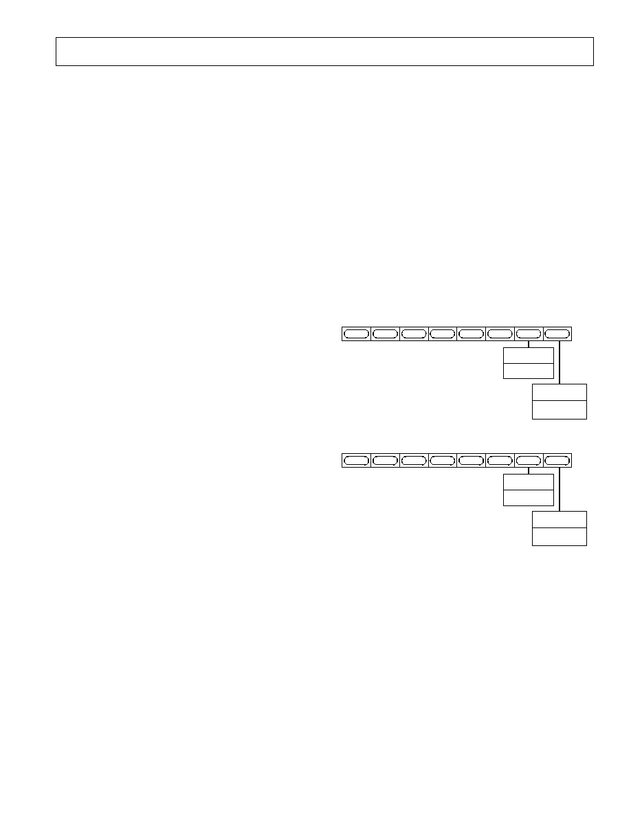
REGISTER ACCESSES
The MPU can write to or read from all of the ADV7175A/
ADV7176A registers except the subaddress register, which is a
write-only register. The subaddress register determines which
register the next read or write operation accesses. All communi-
cations with the part through the bus start with an access to the
subaddress register. A read/write operation is performed from/to
the target address, which then increments to the next address
until a stop command on the bus is performed.
REGISTER PROGRAMMING
The following section describes each register, including subaddress
register, mode registers, subcarrier frequency registers, subcarrier
phase register, timing registers, closed captioning extended data
registers, closed captioning data registers and NTSC pedestal
control registers in terms of its configuration.
Subaddress Register (SR7SR0)
The communications register is an 8-bit write-only register.
After the part has been accessed over the bus, and a read/write
operation is selected, the subaddress is set up. The subaddress
register determines to/from which register the operation takes
place.
Figure 31 shows the various operations under the control of
the subaddress register. Zero should always be written to
SR7SR6.
Register Select (SR5SR0)
These bits are set up to point to the required starting address.
MODE REGISTER 0 MR0 (MR07MR00)
(Address [SR4SR0] = 00H)
Figure 32 shows the various operations under the control of Mode
Register 0. This register can be read from as well as written to.
MR0 BIT DESCRIPTION
Encode Mode Control (MR01MR00)
These bits are used to set up the encode mode. The ADV7175A/
ADV7176A can be set up to output NTSC, PAL (B, D, G, H, I)
and PAL (M) standard video.
Pedestal Control (MR02)
This bit specifies whether a pedestal is to be generated on
the NTSC composite video signal. This bit is invalid if the
ADV7175A/ADV7176A is configured in PAL mode.
Luminance Filter Control (MR04MR03)
The luminance filters are divided into two sets (NTSC/PAL) of
four filters, low-pass A, low-pass B, notch and extended. When
PAL is selected, bits MR03 and MR04 select one of four PAL
luminance filters; likewise, when NTSC is selected, bits MR03
and MR04 select one of four NTSC luminance filters. The fil-
ters are illustrated in Figures 4 to 12.
RGB Sync (MR05)
This bit is used to set up the RGB outputs with the sync infor-
mation encoded on all RGB outputs.
Output Control (MR06)
This bit specifies if the part is in composite video or RGB/YUV
mode. Please note that the main composite signal is still avail-
able in RGB/YUV mode.
MR01
MR00
MR07
MR02
MR04
MR03
MR05
MR06
OUTPUT VIDEO
STANDARD SELECTION
0
0
NTSC
0
1
PAL (B, D, G, H, I)
1
0
PAL (M)
1
1
RESERVED
MR01 MR00
MR07
(0)
ZERO SHOULD
BE WRITTEN TO
THIS BIT
OUTPUT SELECT
0
YC OUTPUT
1
RGB/YUV OUTPUT
MR06
FILTER SELECT
0
0
LOW PASS FILTER (A)
0
1
NOTCH FILTER
1
0
EXTENDED MODE
1
1
LOW PASS FILTER (B)
MR04 MR03
RGB SYNC
0
DISABLE
1
ENABLE
MR05
PEDESTAL CONTROL
0
PEDESTAL OFF
1
PEDESTAL ON
MR02
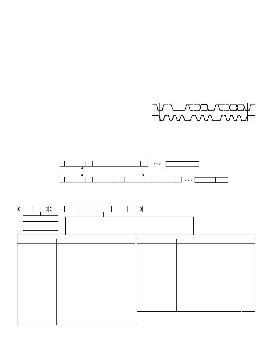
Figure 32. Mode Register 0 (MR0)
MR11
MR10
MR17
MR12
MR13
MR15
MR16
MR14
CLOSED CAPTIONING
FIELD SELECTION
0
0
NO DATA OUT
0
1
ODD FIELD ONLY
1
0
EVEN FIELD ONLY
1
1
DATA OUT
(BOTH FIELDS)
MR12 MR11
DAC A
CONTROL
0
NORMAL
1
POWER-DOWN
MR16
DAC D
CONTROL
MR14
DAC C
CONTROL
MR13
DAC B
CONTROL
MR15
INTERLACE
CONTROL
0
INTERLACED
1
NONINTERLACED
MR10
COLOR BAR
CONTROL
0
DISABLE
1
ENABLE
MR17
0
NORMAL
1
POWER-DOWN
0
NORMAL
1
POWER-DOWN
0
NORMAL
1
POWER-DOWN
Figure 33. Mode Register 1 (MR1)
ADV7175A/ADV7176A
24
REV. B
MODE REGISTER 1 MR1 (MR17MR10)
(Address (SR4SR0) = 01H)
Figure 33 shows the various operations under the control of Mode
Register 1. This register can be read from as well as written to.
MR1 BIT DESCRIPTION
Interlaced Mode Control (MR10)
This bit is used to set up the output to interlaced or noninter-
laced mode. This mode is only relevant when the part is in
composite video mode.
Closed Captioning Field Control (MR12MR11)
These bits control the fields on which closed captioning data is
displayed; closed captioning information can be displayed on an
odd field, even field or both fields.
DAC Control (MR16MR13)
These bits can be used to power down the DACs. This can
be used to reduce the power consumption of the ADV7175A/
ADV7176A if any of the DACs are not required in the application.
Color Bar Control (MR17)
This bit can be used to generate and output an internal color
bar test pattern. The color bar configuration is 75/7.5/75/7.5
for NTSC and 100/0/75/0 for PAL. It is important to note that
when color bars are enabled the ADV7175A/ADV7176A is
configured in a master timing mode as per the one selected by
bits TR01 and TR02.
SUBCARRIER FREQUENCY REGISTER 3-0
(FSC3FSC0)
(Address [SR4SR0] = 05H02H)
These 8-bit wide registers are used to set up the subcarrier fre-
quency. The value of these registers are calculated by using the
following equation:
Subcarrier Frequency Register =
2
32
1
F
CLK
×
F
SCF
i.e.: NTSC Mode,
F
CLK
= 27 MHz,
F
SCF
= 3.5795454 MHz
Subcarrier Frequency Value =
2
32
1
27
×
10
6
×
3.5795454
×
10
6
= 21F07C16 HEX
Figure 34 shows how the frequency is set up by the four registers.
SUBCARRIER
FREQUENCY
REG 3
SUBCARRIER
FREQUENCY
REG 2
SUBCARRIER
FREQUENCY
REG 1
SUBCARRIER
FREQUENCY
REG 0
FSC30
FSC29
FSC27
FSC25
FSC28
FSC24
FSC31
FSC26
FSC22
FSC21
FSC19
FSC17
FSC20
FSC16
FSC23
FSC18
FSC14
FSC13
FSC11
FSC9
FSC12
FSC8
FSC15
FSC10
FSC6
FSC5
FSC3
FSC1
FSC4
FSC0
FSC7
FSC2
Figure 34. Subcarrier Frequency Register
SUBCARRIER PHASE REGISTER (FP7FP0)
(Address [SR4SR0] = 06H)
This 8-bit wide register is used to set up the subcarrier phase.
Each bit represents 1.41
°
.
TIMING REGISTER 0 (TR07TR00)
(Address [SR4SR0] = 07H)
Figure 35 shows the various operations under the control of
Timing Register 0. This register can be read from as well as
written to. This register can be used to adjust the width and
position of the master mode timing signals.
TR0 BIT DESCRIPTION
Master/Slave Control (TR00)
This bit controls whether the ADV7175A/ADV7176A is in
master or slave mode.
Timing Mode Control (TR02TR01)
These bits control the timing mode of the ADV7175A/
ADV7176A. These modes are described in the Timing and
Control section of the data sheet.
BLANK Control (TR03)
This bit controls whether the
BLANK input is used when the
part is in slave mode.
Luma Delay Control (TR05TR04)
These bits control the addition of a luminance delay. Each bit
represents a delay of 74 ns.
Pixel Port Select (TR06)
This bit is used to set the pixel port to accept 8-bit or 16-bit
data. If an 8-bit input is selected the data will be set up on Pins
P7P0.
Timing Register Reset (TR07)
Toggling TR07 from low to high and low again resets the inter-
nal timing counters. This bit should be toggled after power-up,
reset or changing to a new timing mode.
TR01
TR00
TR07
TR02
TR03
TR05
TR06
TR04
TIMING
REGISTER RESET
TR07
BLACK INPUT
CONTROL
0
ENABLE
1
DISABLE
TR03
PIXEL PORT
CONTROL
0
8-BIT
1
16-BIT
TR06
MASTER/SLAVE
CONTROL
0
SLAVE TIMING
1
MASTER TIMING
TR00
LUMA DELAY
0
0
0ns DELAY
0
1
74ns DELAY
1
0
148ns DELAY
1
1
222ns DELAY
TR05 TR04
TIMING MODE
SELECTION
0
0
MODE 0
0
1
MODE 1
1
0
MODE 2
1
1
MODE 3
TR02 TR01
Figure 35. Timing Register 0
ADV7175A/ADV7176A
25
REV. B
CLOSED CAPTIONING EVEN FIELD
DATA REGISTER 10 (CED15CED00)
(Address [SR4SR0] = 0908H)
These 8-bit wide registers are used to set up the closed captioning
extended data bytes on even fields. Figure 36 shows how the
high and low bytes are set up in the registers.
BYTE 1
BYTE 0
CED6
CED5
CED3
CED1
CED4
CED2
CED0
CED7
CED14
CED13
CED11
CED9
CED12
CED10
CED8
CED15
Figure 36. Closed Captioning Extended Data Register
CLOSED CAPTIONING ODD FIELD
DATA REGISTER 10 (CCD15CCD00)
(Subaddress [SR4SR0] = 0B0AH)
These 8-bit wide registers are used to set up the closed captioning
data bytes on odd fields. Figure 37 shows how the high and low
bytes are set up in the registers.
BYTE 1
BYTE 0
CCD6
CCD5
CCD3
CCD1
CCD4
CCD2
CCD0
CCD7
CCD14
CCD13
CCD11
CCD9
CCD12
CCD10
CCD8
CCD15
Figure 37. Closed Captioning Data Register
TIMING REGISTER 1 (TR17TR10)
(ADDRESS [SR4SR0] = 0CH)
Timing Register 1 is an 8-Bit Wide Register
Figure 38 shows the various operations under the control of
Timing Register 1. This register can be read from as well as
written to. This register can be used to adjust the width and
position of the master mode timing signals.
TR1 BIT DESCRIPTION
HSYNC Width (TR11TR10)
These bits adjust the
HSYNC pulsewidth.
HSYNC to VSYNC/FIELD Delay Control (TR13TR12)
These bits adjust the position of the
HSYNC output relative to
the FIELD/
VSYNC output.
HSYNC to FIELD Delay Control (TR15TR14)
When the ADV7175A/ADV7176A is in Timing Mode 1, these
bits adjust the position of the
HSYNC output relative to the
FIELD output rising edge.
VSYNC Width (TR15TR14)
When the ADV7175A/ADV7176A is in Timing Mode 2, these
bits adjust the
VSYNC pulsewidth.
HSYNC to Pixel Data Adjust (TR17TR16)
This enables the
HSYNC to be adjusted with respect to the
pixel data. This allows the Cr and Cb components to be
swapped. This adjustment is available in both master and slave
timing modes.
MODE REGISTER 2 MR2 (MR27MR20)
(Address [SR4-SR0] = 0DH)
Mode Register 2 is an 8-bit wide register.
Figure 39 shows the various operations under the control of Mode
Register 2. This register can be read from as well as written to.
MR2 BIT DESCRIPTION
Square Pixel Mode Control (MR20)
This bit is used to set up square pixel mode. This is available in
slave mode only. For NTSC, a 24.54 MHz clock must be sup-
plied. For PAL, a 29.5 MHz clock must be supplied.
TR11
TR10
TR17
TR12
TR13
TR15
TR16
TR14
HSYNC
WIDTH
0
0
1 x T
PCLK
0
1
4 x T
PCLK
1
0
16 x T
PCLK
1
1
128 x T
PCLK
TR11 TR10
T
A
HSYNC
TO FIELD
RISING EDGE DELAY
(MODE 1 ONLY)
x
0
T
B
x
1
T
B
+ 32 s
TR15 TR14
T
C
HSYNC
TO PIXEL
DATA ADJUSTMENT
TR17 TR16
0
0
0 x T
PCLK
0
1
1 x T
PCLK
1
0
2 x T
PCLK
1
1
3 x T
PCLK
HSYNC
TO
FIELD/
VSYNC
DELAY
TR13 TR12
0
0
0 x T
PCLK
0
1
4 x T
PCLK
1
0
8 x T
PCLK
1
1
16 x T
PCLK
VSYNC WIDTH
(MODE 2 ONLY)
TR15 TR14
0
0
1 x T
PCLK
0
1
4 x T
PCLK
1
0
16 x T
PCLK
1
1
128 x T
PCLK
LINE 313
LINE 314
LINE 1
T
B
TIMING MODE 1 (MASTER/PAL)
HSYNC
FIELD/
VSYNC
T
A
T
C
T
B
Figure 38. Timing Register 1
ADV7175A/ADV7176A
26
REV. B
Genlock Control (MR22MR21)
These bits control the genlock feature of the ADV7175A/
ADV7176A. Setting MR21 to a Logic "1" configures the
SCRESET/RTC pin as an input. Setting MR22 to Logic Level
"0" configures the SCRESET/RTC pin as a subcarrier reset
input, therefore, the subcarrier will reset to Field 0, following a
high-to-low transition on the SCRESET/RTC pin. Setting
MR22 to Logic Level "1" configures the SCRESET/RTC pin as
a real-time control input.
Active Video Line Control (MR23)
This bit switches between two active video line durations. A
zero selects ITU-R BT.470 (720 pixels PAL/NTSC) and a one
selects ITU-R/SMPTE "analog" standard for active video dura-
tion (710 pixels NTSC 702 pixels PAL).
Chrominance Control (MR24)
This bit enables the color information to be switched on and off
the video output.
Burst Control (MR25)
This bit enables the burst information to be switched on and off
the video output.
RGB/YUV Control (MR26)
This bit enables the output from the RGB DACs to be set to
YUV output video standard. Bit MR06 of Mode Register 0
must be set to Logic Level "1" before MR26 is set.
Lower Power Control (MR27)
This bit enables the lower power mode of the ADV7175A/
ADV7176A. This will reduce the DAC current by 50%.
NTSC PEDESTAL/PAL TELETEXT CONTROL
REGISTERS 30 (PCE150, PCO150)/ (TXE150, TXO150)
(Subaddress [SR4SR0] = 110EH)
These 8-bit wide registers are used to set up the NTSC pedes-
tal/PAL teletext on a line-by-line basis in the vertical blanking
interval for both odd and even fields. Figures 40 and 41 show
the four control registers. A Logic "1" in any of the bits of these
registers has the effect of turning the pedestal OFF on the
equivalent line when used in NTSC. A Logic "1" in any of the
bits of these registers has the effect of turning teletext ON the
equivalent line when used in PAL.
FIELD 1/3
PCO6
PCO5
PCO3
PCO1
PCO4
PCO2
PCO0
PCO7
LINE 17 LINE 16 LINE 15 LINE 14 LINE 13 LINE 12 LINE 11 LINE 10
PCO14
PCO13
PCO11
PCO9
PCO12
PCO10
PCO8
PCO15
LINE 25 LINE 24 LINE 23 LINE 22 LINE 21 LINE 20 LINE 19 LINE 18
FIELD 1/3
FIELD 2/4
PCE6
PCE5
PCE3
PCE1
PCE4
PCE2
PCE0
PCE7
LINE 17 LINE 16 LINE 15 LINE 14 LINE 13 LINE 12 LINE 11 LINE 10
PCE14
PCE13
PCE11
PCE9
PCE12
PCE10
PCE8
PCE15
LINE 25 LINE 24 LINE 23 LINE 22 LINE 21 LINE 20 LINE 19 LINE 18
FIELD 2/4
Figure 40. Pedestal Control Registers
FIELD 1/3
FIELD 1/3
FIELD 2/4
FIELD 2/4
TXO6
TXO5
TXO3
TXO1
TXO4
TXO2
TXO0
TXO7
LINE 14 LINE 13 LINE 12 LINE 11 LINE 10 LINE 9
LINE 8 LINE 7
TXO14
TXO13
TXO11
TXO9
TXO12
TXO10
TXO8
TXO15
LINE 22 LINE 21 LINE 20 LINE 19 LINE 18 LINE 17 LINE 16 LINE 15
TXE6
TXE5
TXE3
TXE1
TXE4
TXE2
TXE0
TXE7
TXE14
TXE13
TXE11
TXE9
TXE12
TXE10
TXE8
TXE15
LINE 14 LINE 13 LINE 12 LINE 11 LINE 10 LINE 9
LINE 8
LINE 7
LINE 22 LINE 21 LINE 20 LINE 19 LINE 18 LINE 17 LINE 16 LINE 15
Figure 41. Teletext Control Registers
MODE REGISTER 3 MR3 (MR37MR30)
(Address [SR4SR0] = 12H)
Mode Register 3 is an 8-bit wide register.
Figure 42 shows the various operations under the control of
Mode Register 3.
MR3 BIT DESCRIPTION
Revision Code (MR30)
This bit is read only and indicates the revision of the device.
VBI Pass-Through Control (MR31)
This bit determines whether or not data in the vertical blanking
interval (VBI) is output to the analog outputs or blanked.
Reserved (MR33MR32)
These bits are reserved.
Teletext Enable (MR34)
This bit must be set to "1" to enable teletext data insertion on
the TTX pin.
MR21
MR27
MR22
MR23
MR26
MR25
MR24
MR20
CHROMINANCE
CONTROL
0
ENABLE COLOR
1
DISABLE COLOR
MR24
GENLOCK SELECTION
x
0
DISABLE GENLOCK
0
1
ENABLE SUBCARRIER
RESET PIN
1
1
ENABLE RTC PIN
MR22 MR21
RGB/YUV
CONTROL
0
RGB OUTPUT
1
YUV OUTPUT
MR26
SQUARE PIXEL
CONTROL
0
DISABLE
1
ENABLE
MR20
BURST
CONTROL
0
ENABLE BURST
1
DISABLE BURST
MR25
LOWER POWER
MODE
0
DISABLE
1
ENABLE
MR27
ACTIVE VIDEO LINE WIDTH
CONTROL
0
720 PIXELS ACTIVE LINE
1
ITU-R/SMPTE ACTIVE LINE
MR23
Figure 39. Mode Register 2
ADV7175A/ADV7176A
27
REV. B
Table I. DAC Output Configuration Matrix
MR06
MR26
MR37
DAC A
DAC B
DAC C
DAC D
Simultaneous Output
0
0
0
CVBS
CVBS
C
Y
2 Composite and Y/C
0
0
1
Y
CVBS
C
CVBS
2 Composite and Y/C
0
1
0
CVBS
CVBS
C
Y
2 Composite and Y/C
0
1
1
Y
CVBS
C
CVBS
2 Composite and Y/C
1
0
0
CVBS
B
R
G
RGB and Composite
1
0
1
G
B
R
CVBS
RGB and Composite
1
1
0
CVBS
U
V
Y
YUV and Composite
1
1
1
Y
U
V
CVBS
YUV and Composite
TELETEXT CONTROL REGISTER TC07 (TC07TC00)
(Address [SR4SR0] = 24H)
Teletext Control Register is an 8-bit wide register.
TTXREQ Rising Edge Control (TC07TC04)
These bits control the position of the rising edge of TTXREQ.
It can be programmed from zero CLOCK cycles to a max of 15
CLOCK cycles--see Figure 48.
TTXREQ Falling Edge Control (TC03TC00)
These bits control the position of the falling edge of TTXREQ.
It can be programmed from zero CLOCK cycles to a max of 15
CLOCK cycles. This controls the active window for teletext
data. Increasing this value reduces the amount of teletext bits
below the default of 360. If bits TC03TC00 are unchanged
when bits TC07TC04 are changed, the falling edge of TTREQ
will track that of the rising edge (i.e., the time between the fall-
ing and rising edge remains constant)--see Figure 48.
Figure 43. Teletext Control Register
TC01
TC00
TC07
TC02
TC04
TC03
TC05
TC06
TTXR EQ RISING EDGE CONTROL
TC07 TC06
TC05 TC04
0
0
0
0
0 PCLK
0
0
0
1
1 PCLK
"
"
"
"
" PCLK
1
1
1
0
14 PCLK
1
1
1
1
15 PCLK
TTXR EQ FALLING EDGE CONTROL
TC03 TC02
TC01 TC00
0
0
0
0
0 PCLK
0
0
0
1
1 PCLK
"
"
"
"
" PCLK
1
1
1
0
14 PCLK
1
1
1
1
15 PCLK
Input Default Color (MR36)
This bit determines the default output color from the DACs for
zero input data (or disconnected). A Logical "0" means that the
color corresponding to 00000000 will be displayed. A Logical
"1" forces the output color to black for 00000000 input video
data.
DAC Switching Control (MR37)
This bit is used to switch the DAC outputs from SCART to a
EUROSCART configuration. A complete table of all DAC
output configurations is shown below.
CVBS: Composite Video Baseband Signal
Y:
Luminance Component Signal (For YUV or Y/C Mode)
C:
Chrominance Signal (For Y/C Mode)
U:
Chrominance Component Signal (For YUV Mode)
V:
Chrominance Component Signal (For YUV Mode)
R:
RED Component Video (For RGB Mode)
G:
GREEN Component Video (For RGB Mode)
B:
BLUE Component Video (For RGB Mode)
MR31
MR30
MR37
MR32
MR34
MR33
MR35
MR36
MR30
REV CODE
(READ ONLY)
INPUT DEFAULT COLOR
0
INPUT COLOR
1
BLACK
MR36
VBI PASSTHROUGH
0
DISABLE
1
ENABLE
MR31
RESERVED
TELETEXT ENABLE
0
DISABLE
1
ENABLE
MR34
MR35 = 0
ZERO SHOULD
BE WRITTEN TO
THIS BIT
DAC OUTPUT
SWITCHING
0
COMPOSITE
1
GREEN/LUMA/Y
MR37
DAC A
BLUE/COMP/U
BLUE/COMP/U
DAC B
RED/CHROMA/V
RED/CHROMA/V
DAC C
GREEN/LUMA/Y
COMPOSITE
DAC D
Figure 42. Mode Register 3
NOTE
Each DAC can be individually powered ON or OFF with the following control bits
("0" = ON, "1" = OFF):
MR13 - DAC C
MR14 - DAC D
MR15 - DAC B
MR16 - DAC A

ADV7175A/ADV7176A
28
REV. B
APPENDIX 1
BOARD DESIGN AND LAYOUT CONSIDERATIONS
The ADV7175A/ADV7176A is a highly integrated circuit contain-
ing both precision analog and high speed digital circuitry. It has
been designed to minimize interference effects on the integrity
of the analog circuitry by the high speed digital circuitry. It is
imperative that these same design and layout techniques be
applied to the system level design so that high speed, accurate
performance is achieved. The "Recommended Analog Circuit
Layout" shows the analog interface between the device and
monitor.
The layout should be optimized for lowest noise on the ADV7175A/
ADV7176A power and ground lines by shielding the digital
inputs and providing good decoupling. The lead length between
groups of V
AA
and GND pins should by minimized to minimize
inductive ringing.
Ground Planes
The ground plane should encompass all ADV7175A/ADV7176A
ground pins, voltage reference circuitry, power supply bypass
circuitry for the ADV7175A/ADV7176A, the analog output traces,
and all the digital signal traces leading up to the ADV7175A/
ADV7176A. The ground plane is the board's common ground
plane.
This should be as substantial as possible to maximize heat
spreading and power dissipation on the board.
Power Planes
The ADV7175A/ADV7176A and any associated analog circuitry
should have its own power plane, referred to as the analog
power plane (V
AA
). This power plane should be connected to
the regular PCB power plane (V
CC
) at a single point through a
ferrite bead. This bead should be located within three inches of
the ADV7175A/ADV7176A.
The metallization gap separating device power plane and board
power plane should be as narrow as possible to minimize the
obstruction to the flow of heat from the device into the general
board.
The PCB power plane should provide power to all digital logic
on the PC board, and the analog power plane should provide
power to all ADV7175A/ADV7176A power pins and voltage
reference circuitry.
Plane-to-plane noise coupling can be reduced by ensuring that
portions of the regular PCB power and ground planes do not
overlay portions of the analog power plane unless they can be
arranged so that the plane-to-plane noise is common-mode.
Supply Decoupling
For optimum performance, bypass capacitors should be in-
stalled using the shortest leads possible, consistent with reliable
operation, to reduce the lead inductance. Best performance is
obtained with 0.1
µ
F ceramic capacitor decoupling. Each
group of V
AA
pins on the ADV7175A/ADV7176A must have at
least one 0.1
µ
F decoupling capacitor to GND. These capaci-
tors should be placed as close to the device as possible.
It is important to note that while the ADV7175A/ADV7176A
contains circuitry to reject power supply noise, this rejection
decreases with frequency. If a high frequency switching power
supply is used, the designer should pay close attention to reduc-
ing power supply noise and consider using a three terminal voltage
regulator for supplying power to the analog power plane.
Digital Signal Interconnect
The digital inputs to the ADV7175A/ADV7176A should be
isolated as much as possible from the analog outputs and other
analog circuitry. Also, these input signals should not overlay
the analog power plane.
Due to the high clock rates involved, long clock lines to the
ADV7175A/ADV7176A should be avoided to reduce noise
pickup.
Any active termination resistors for the digital inputs should be
connected to the regular PCB power plane (V
CC
) and not the
analog power plane.
Analog Signal Interconnect
The ADV7175A/ADV7176A should be located as close to the
output connectors as possible to minimize noise pickup and
reflections due to impedance mismatch.
The video output signals should overlay the ground plane, not
the analog power plane, to maximize the high frequency power
supply rejection.
Digital inputs, especially pixel data inputs and clocking signals,
should never overlay any of the analog signal circuitry and
should be kept as far away as possible.
For best performance, the outputs should each have a 75
load resistor connected to GND. These resistors should be
placed as close as possible to the ADV7175A/ADV7176A as to
minimize reflections.
The ADV7175A/ADV7176A should have no inputs left float-
ing. Any inputs that are not required should be tied to ground.
ADV7175A/ADV7176A
29
REV. B
75
27
26
S VIDEO
31
32
5k
+5V (V
CC
)
150
24
5k
+5V (V
CC
)
MPU BUS
44
22
15
17
16
10, 19, 21
29, 43
18
23
34
3842,
29, 1214
1, 11, 20, 28, 30
0.1 F
0.01 F
0.1 F
+5V (V
AA
)
0.1 F
+5V (V
AA
)
10k
+5V (V
AA
)
27MHz CLOCK
(SAME CLOCK AS USED BY
MPEG2 DECODER)
POWER SUPPLY DECOUPLING
FOR EACH POWER SUPPLY GROUP
10 F
33 F
GND
L1
(FERRITE BEAD)
+5V
25
33
GND
ALSB
HSYNC
FIELD/
VSYNC
BLANK
RESET
CLOCK
R
SET
SDATA
SCLOCK
DAC B
DAC C
DAC D
V
AA
V
REF
COMP
P15P0
+5V (V
AA
)
75
75
75
35 SCRESET/RTC
ADV7175A
ADV7176A
"UNUSED
INPUTS
SHOULD BE
GROUNDED"
DAC A
100
100
4k
+5V (V
AA
)
100nF
RESET
37 TTX
36 TTX REQ
(V
CC
)
100k
100k
+5V (V
CC
)
TTX
TTX REQ
TELETEXT PULLUP &
PULLDOWN RESISTORS
SHOULD ONLY BE USED
IF THESE PINS ARE NOT
CONNECTED
Figure 44. Recommended Analog Circuit Layout
The circuit below can be used to generate a 13.5 MHz waveform using the 27 MHz clock and the
HSYNC pulse. This waveform is
guaranteed to produce the 13.5 MHz clock in synchronization with the 27 MHz clock. This 13.5 MHz clock can be used if the
13.5 MHz clock is required by the MPEG decoder. This will guarantee that the Cr and Cb pixel information is input to the
ADV7175A/ADV7176A in the correct sequence.
D
Q
CK
D
Q
CK
CLOCK
HSYNC
13.5MHz
Figure 45. Circuit to Generate 13.5 MHz
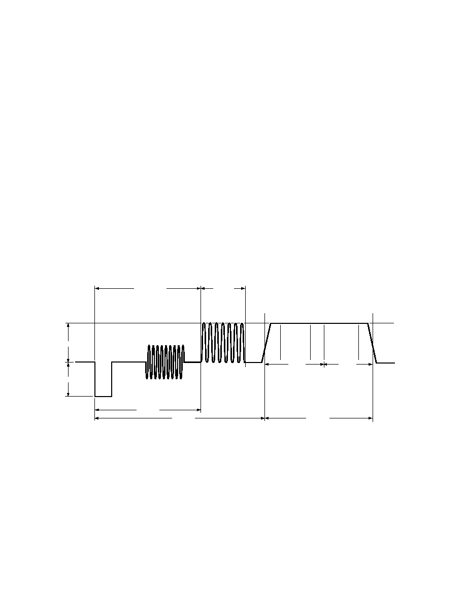
ADV7175A/ADV7176A
30
REV. B
The ADV7175A/ADV7176A supports closed captioning, conforming to the standard television synchronizing waveform for color
transmission. Closed captioning is transmitted during the blanked active line time of Line 21 of the odd fields and Line 284 of even
fields.
Closed captioning consists of a 7-cycle sinusoidal burst that is frequency and phase locked to the caption data. After the clock run-in
signal, the blanking level is held for two data bits and is followed by a Logic Level "1" start bit. 16 bits of data follow the start bit.
These consist of two 8-bit bytes, seven data bits and one odd parity bit. The data for these bytes is stored in closed captioning Data
Registers 0 and 1.
The ADV7175A/ADV7176A also supports the extended closed captioning operation, which is active during even fields, and is en-
coded on scan Line 284. The data for this operation is stored in closed captioning extended Data Registers 0 and 1.
All clock run-in signals and timing to support closed captioning on Lines 21 and 284 are generated automatically by the ADV7175A/
ADV7176A. All pixels inputs are ignored during Lines 21 and 284.
FCC Code of Federal Regulations (CFR) 47 Section 15.119 and EIA608 describe the closed captioning information for Lines 21 and
284.
The ADV7175A/ADV7176A uses a single buffering method. This means that the closed captioning buffer is only one byte deep,
therefore there will be no frame delay in outputting the closed captioning data unlike other 2-byte deep buffering systems. The data
must be loaded at least one line before (Line 20 or Line 283) it is outputted on Line 21 and Line 284. A typical implementation of
this method is to use
VSYNC to interrupt a microprocessor, which will in turn load the new data (two bytes) every field. If no new
data is required for transmission you must insert zeros in both the data registers; this is called NULLING. It is also important to load
"control codes," all of which are double bytes on Line 21, or a TV will not recognize them. If you have a message like "Hello World"
which has an odd number of characters, it is important to pad it out to an even number to get "end of caption" 2-byte control code to
land in the same field.
12.91 s
S
T
A
R
T
P
A
R
I
T
Y
P
A
R
I
T
Y
D0D6
D0D6
10.003 s
33.764 s
50 IRE
40 IRE
FREQUENCY = F
SC
= 3.579545MHz
AMPLITUDE = 40 IRE
REFERENCE COLOR BURST
(9 CYCLES)
7 CYCLES
OF 0.5035 MHz
(CLOCKRUN-IN)
10.5 0.25 s
TWO 7-BIT + PARITY
ASCII CHARACTERS
(DATA)
27.382 s
BYTE 0
BYTE 1
Figure 46. Closed Captioning Waveform (NTSC)
APPENDIX 2
CLOSED CAPTIONING
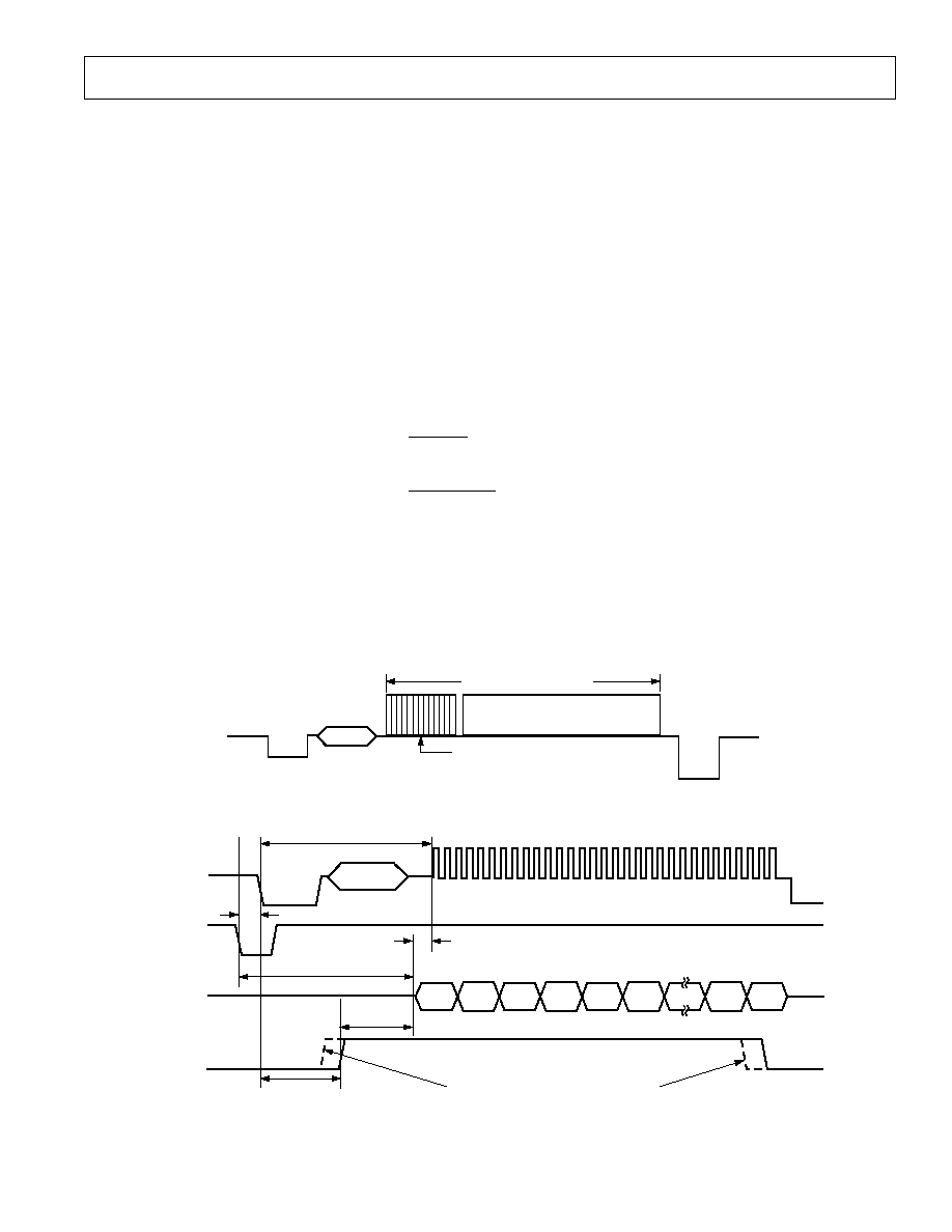
ADV7175A/ADV7176A
31
REV. B
APPENDIX 3
TELETEXT INSERTION
Time T
PD
time needed by the ADV7175A/ADV7176A to interpolate input data on TTX and insert it onto the CVBS or Y outputs,
such that it appears T
synTxtOut
= 10.2
µ
s after the leading edge of the horizontal signal. Time Txt
Del
is the pipeline delay time by the
source that is gated by the TTREQ signal in order to deliver TTX data.
With the programmability that is offered with TTXREQ signal on the Rising/Falling edges, the TTX data is always inserted at the
correct position of 10.2
µ
s after the leading edge of Horizontal Sync pulse, which enables a source interface with variable pipeline
delays.
The width of the TTXREQ signal must always be maintained so it allows the insertion of 360 (to comply with the Teletext Standard
"PALWST") teletext bits at a text data rate of 6.9375 Mbits/s; this is achieved by setting TC03TC00 to zero. The insertion win-
dow is not open if the Teletext Enable bit (MR34) is set to zero.
Teletext Protocol
The relationship between the TTX bit clock (6.9375 MHz) and the system CLOCK (27 MHz) for 50 Hz is given as follows:
27 MHz
4
=
6.75 MHz
6.9375
×
10
6
6.75
×
10
6
=
1.027777
Thus 37 TTX bits correspond to 144 clocks (27 MHz) and each bit has a width of almost four clock cycles. The ADV7175A/ADV7176A
uses an internal sequencer and variable phase interpolation filter to minimize the phase jitter and thus generate a bandlimited signal
which can be outputted on the CVBS and Y outputs.
At the TTX input the bit duration scheme repeats after every 37 TTX bits or 144 clock cycles. The protocol requires that TTX bits
10, 19, 28, 37 are carried by three clock cycles, all other bits by four clock cycles. After 37 TTX bits, the next bits with three clock
cycles are 47, 56, 65 and 74. This scheme holds for all following cycles of 37 TTX bits, until all 360 TTX bits are completed. All
teletext lines are implemented in the same way. Individual control of teletext lines are controlled by Teletext Setup Registers.
ADDRESS & DATA
RUN-IN CLOCK
TELETEXT VBI LINE
45 BYTES (360 BITS) PAL
Figure 47. Teletext VBI Line
PROGRAMMABLE PULSE EDGES
t
SYNTXTOUT
t
PD
t
PD
10.2 s
TXT
ST
TXT
DEL
CVBS/Y
HSYNC
TXTREQ
TXT
DATA
t
SYNTXTOUT
= 10.2 s
t
PD
= PIPELINE DELAY THROUGH ADV7175A/ADV7176A
TXT
DEL
= TTXREQ TO TTX (PROGRAMMABLE RANGE = 4 BITS [015 CLOCK CYCLES])
Figure 48. Teletext Functionality Diagram
ADV7175A/ADV7176A
32
REV. B
APPENDIX 4
NTSC WAVEFORMS (WITH PEDESTAL)
130.8 IRE
100 IRE
7.5 IRE
0 IRE
40 IRE
PEAK COMPOSITE
REF WHITE
BLACK LEVEL
SYNC LEVEL
BLANK LEVEL
714.2mV
1268.1mV
1048.4mV
387.6mV
334.2mV
48.3mV
Figure 49. NTSC Composite Video Levels
100 IRE
7.5 IRE
0 IRE
40 IRE
REF WHITE
BLACK LEVEL
SYNC LEVEL
BLANK LEVEL
714.2mV
1048.4mV
387.6mV
334.2mV
48.3mV
Figure 50. NTSC Luma Video Levels
650mV
232.2mV
1067.7mV
0mV
PEAK CHROMA
BLANK/BLACK LEVEL
286mV (pk-pk)
835mV (pk-pk)
PEAK CHROMA
Figure 51. NTSC Chroma Video Levels
100 IRE
7.5 IRE
0 IRE
40 IRE
REF WHITE
BLACK LEVEL
SYNC LEVEL
BLANK LEVEL
720.8mV
1052.2mV
387.5mV
331.4mV
45.9mV
Figure 52. NTSC RGB Video Levels
ADV7175A/ADV7176A
33
REV. B
NTSC WAVEFORMS (WITHOUT PEDESTAL)
130.8 IRE
100 IRE
0 IRE
40 IRE
PEAK COMPOSITE
REF WHITE
SYNC LEVEL
BLANK/BLACK LEVEL
714.2mV
1289.8mV
1052.2mV
338mV
52.1mV
Figure 53. NTSC Composite Video Levels
100 IRE
0 IRE
40 IRE
REF WHITE
SYNC LEVEL
BLANK/BLACK LEVEL
714.2mV
1052.2mV
338mV
52.1mV
Figure 54. NTSC Luma Video Levels
650mV
198.4mV
1101.6mV
0mV
PEAK CHROMA
BLANK/BLACK LEVEL
307mV (pk-pk)
903.2mV (pk-pk)
PEAK CHROMA
Figure 55. NTSC Chroma Video Levels
100 IRE
0 IRE
40 IRE
REF WHITE
SYNC LEVEL
BLANK/BLACK LEVEL
715.7mV
1052.2mV
336.5mV
51mV
Figure 56. NTSC RGB Video Levels
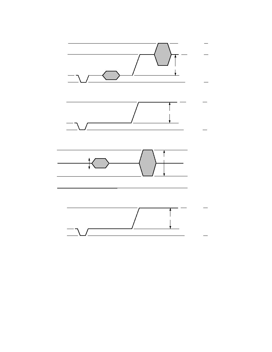
ADV7175A/ADV7176A
34
REV. B
PAL WAVEFORMS
1284.2mV
1047.1mV
350.7mV
50.8mV
PEAK COMPOSITE
REF WHITE
SYNC LEVEL
BLANK/BLACK LEVEL
696.4mV
Figure 57. PAL Composite Video Levels
1047mV
350.7mV
50.8mV
REF WHITE
SYNC LEVEL
BLANK/BLACK LEVEL
696.4mV
Figure 58. PAL Luma Video Levels
650mV
207.5mV
1092.5mV
0mV
PEAK CHROMA
BLANK/BLACK LEVEL
300mV (pk-pk)
885mV (pk-pk)
PEAK CHROMA
Figure 59. PAL Chroma Video Levels
1050.2mV
351.8mV
51mV
REF WHITE
SYNC LEVEL
BLANK/BLACK LEVEL
698.4mV
Figure 60. PAL RGB Video Levels
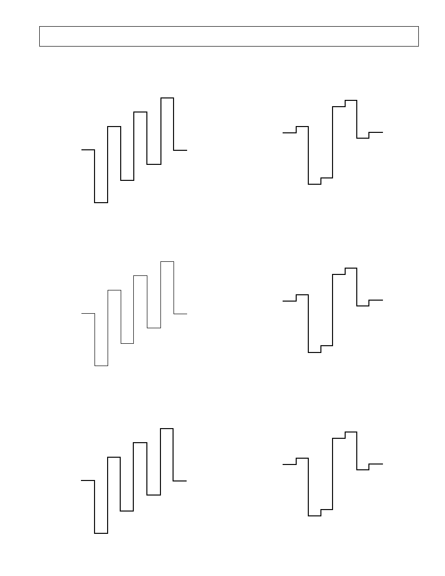
ADV7175A/ADV7176A
35
REV. B
UV WAVEFORMS
BETACAM LEVEL
0mV
171mV
334mV
505mV
0mV
171mV
334mV
505mV
WHITE
YELLOW
CYAN
GREEN
MAGENTA
RED
BLUE
BLACK
Figure 61. NTSC 100% Color Bars No Pedestal U Levels
BETACAM LEVEL
0mV
158mV
309mV
467mV
0mV
158mV
309mV
467mV
WHITE
YELLOW
CYAN
GREEN
MAGENTA
RED
BLUE
BLACK
Figure 62. NTSC 100% Color Bars with Pedestal U Levels
SMPTE LEVEL
0mV
118mV
232mV
350mV
0mV
118mV
232mV
350mV
WHITE
YELLOW
CYAN
GREEN
MAGENTA
RED
BLUE
BLACK
Figure 63. PAL 1005 Color Bars U Levels
BETACAM LEVEL
0mV
82mV
423mV
505mV
0mV
82mV
505mV
423mV
WHITE
YELLOW
CYAN
GREEN
MAGENTA
RED
BLUE
BLACK
Figure 64. NTSC 100% Color Bars No Pedestal V Levels
BETACAM LEVEL
0mV
76mV
391mV
467mV
0mV
76mV
467mV
391mV
WHITE
YELLOW
CYAN
GREEN
MAGENTA
RED
BLUE
BLACK
Figure 65. NTSC 100% Color Bars with Pedestal V Levels
SMPTE LEVEL
0mV
57mV
293mV
350mV
0mV
57mV
350mV
293mV
WHITE
YELLOW
CYAN
GREEN
MAGENTA
RED
BLUE
BLACK
Figure 66. PAL 100% Color Bars V Levels

ADV7175A/ADV7176A
36
REV. B
APPENDIX 5
REGISTER VALUES
The ADV7175A/ADV7176A registers can be set depending on
the user standard required.
The following examples give the various register formats for
several video standards.
In each case the output is set to composite o/p with all DACs
powered up and with the
BLANK input control disabled. Addi-
tionally, the burst and color information are enabled on the
output and the internal color bar generator is switched off. In
the examples shown, the timing mode is set to Mode 0 in slave
format. TR02TR00 of the Timing Register 0 control the tim-
ing modes. For a detailed explanation of each bit in the com-
mand registers, please turn to the Register Programming section
of the data sheet. TR07 should be toggled after setting up a new
timing mode. Timing Register 1 provides additional control over
the position and duration of the timing signals. In the examples,
this register is programmed in default mode.
NTSC (F
SC
= 3.5795454 MHz)
Address
Data
00Hex
Mode Register 0
04Hex
01Hex
Mode Register 1
00Hex
02Hex
Subcarrier Frequency Register 0
16Hex
03Hex
Subcarrier Frequency Register 1
7CHex
04Hex
Subcarrier Frequency Register 2
F0Hex
05Hex
Subcarrier Frequency Register 3
21Hex
06Hex
Subcarrier Phase Register
00Hex
07Hex
Timing Register 0
08Hex
08Hex
Closed Captioning Ext Register 0
00Hex
09Hex
Closed Captioning Ext Register 1
00Hex
0AHex
Closed Captioning Register 0
00Hex
0BHex
Closed Captioning Register 1
00Hex
0CHex
Timing Register 1
00Hex
0DHex
Mode Register 2
00Hex
0EHex
Pedestal Control Register 0
00Hex
0FHex
Pedestal Control Register 1
00Hex
10Hex
Pedestal Control Register 2
00Hex
11Hex
Pedestal Control Register 3
00Hex
12Hex
Mode Register 3
00Hex
24Hex
Teletext Control Register
00Hex
PAL B, D, G, H, I (F
SC
= 4.43361875 MHz)
Address
00Hex
Mode Register 0
01 Hex
01Hex
Mode Register 1
00 Hex
02Hex
Subcarrier Frequency Register 0
CBHex
03Hex
Subcarrier Frequency Register 1
8A Hex
04Hex
Subcarrier Frequency Register 2
09 Hex
05Hex
Subcarrier Frequency Register 3
2AHex
06Hex
Subcarrier Phase Register
00 Hex
07Hex
Timing Register 0
08 Hex
08Hex
Closed Captioning Ext Register 0
00 Hex
09Hex
Closed Captioning Ext Register 1
00 Hex
0AHex
Closed Captioning Register 0
00 Hex
0BHex
Closed Captioning Register 1
00 Hex
0CHex
Timing Register 1
00 Hex
0DHex
Mode Register 2
00 Hex
0EHex
Pedestal Control Register 0
00 Hex
0FHex
Pedestal Control Register 1
00 Hex
Address
Data
10Hex
Pedestal Control Register 2
00Hex
11Hex
Pedestal Control Register 3
00Hex
12Hex
Mode Register 3
00Hex
24Hex
Teletext Control Register
00Hex
PAL M (F
SC
= 3.57561149 MHz)
Address
Data
00Hex
Mode Register 0
06Hex
01Hex
Mode Register 1
00Hex
02Hex
Subcarrier Frequency Register 0
A3Hex
03Hex
Subcarrier Frequency Register 1
EFHex
04Hex
Subcarrier Frequency Register 2
E6Hex
05Hex
Subcarrier Frequency Register 3
21Hex
06Hex
Subcarrier Phase Register
00Hex
07Hex
Timing Register 0
08Hex
08Hex
Closed Captioning Ext Register 0
00Hex
09Hex
Closed Captioning Ext Register 1
00Hex
0AHex
Closed Captioning Register 0
00Hex
0BHex
Closed Captioning Register 1
00Hex
0CHex
Timing Register 1
00Hex
0DHex
Mode Register 2
00Hex
0EHex
Pedestal Control Register 0
00Hex
0FHex
Pedestal Control Register 1
00Hex
10Hex
Pedestal Control Register 2
00Hex
11Hex
Pedestal Control Register 3
00Hex
12Hex
Mode Register 3
00Hex
24Hex
Teletext Control Register
00Hex
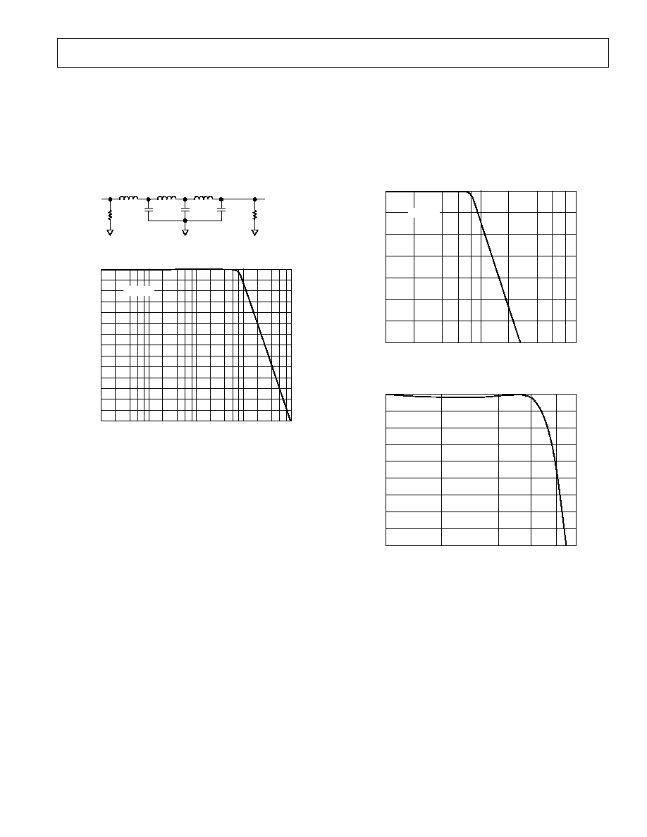
ADV7175A/ADV7176A
37
REV. B
If an output filter is required for the CVBS, Y, UV, Chroma and RGB outputs of the ADV7175A/ADV7176A, the following filter in
Figure 67 can be used. Plots of the filter characteristics are shown in Figures 68, 69 and 70. An output filter is not required if the
outputs of the ADV7175A/ADV7176A are connected to an analog monitor or an analog TV; however, if the output signals are ap-
plied to a system where sampling is used (e.g., digital TV), a filter is required to prevent aliasing.
APPENDIX 6
OPTIONAL OUTPUT FILTER
L
1 H
L
2.7 H
L
0.68 H
R
75
R
75
C
470pF
C
330pF
C
56pF
IN
OUT
Figure 67. Output Filter
FREQUENCY Hz
10k
100M
100k
DECIBELS
1M
10M
0
5
70
10
15
20
25
30
35
40
45
50
55
60
65
V
dB
OP
Figure 68. Output Filter Plot
FREQUENCY MHz
1
100
DECIBELS
10
0
35
5
10
15
20
25
30
V
dB
OP
Figure 69. Output Filter Close Up
FREQUENCY MHz
1
10
DECIBELS
2
0.0
3.5
0.5
1.0
1.5
2.0
2.5
3.0
V
dB
OP
4
6
8
4.5
4.0
Figure 70. Output Filter Plot Close Up
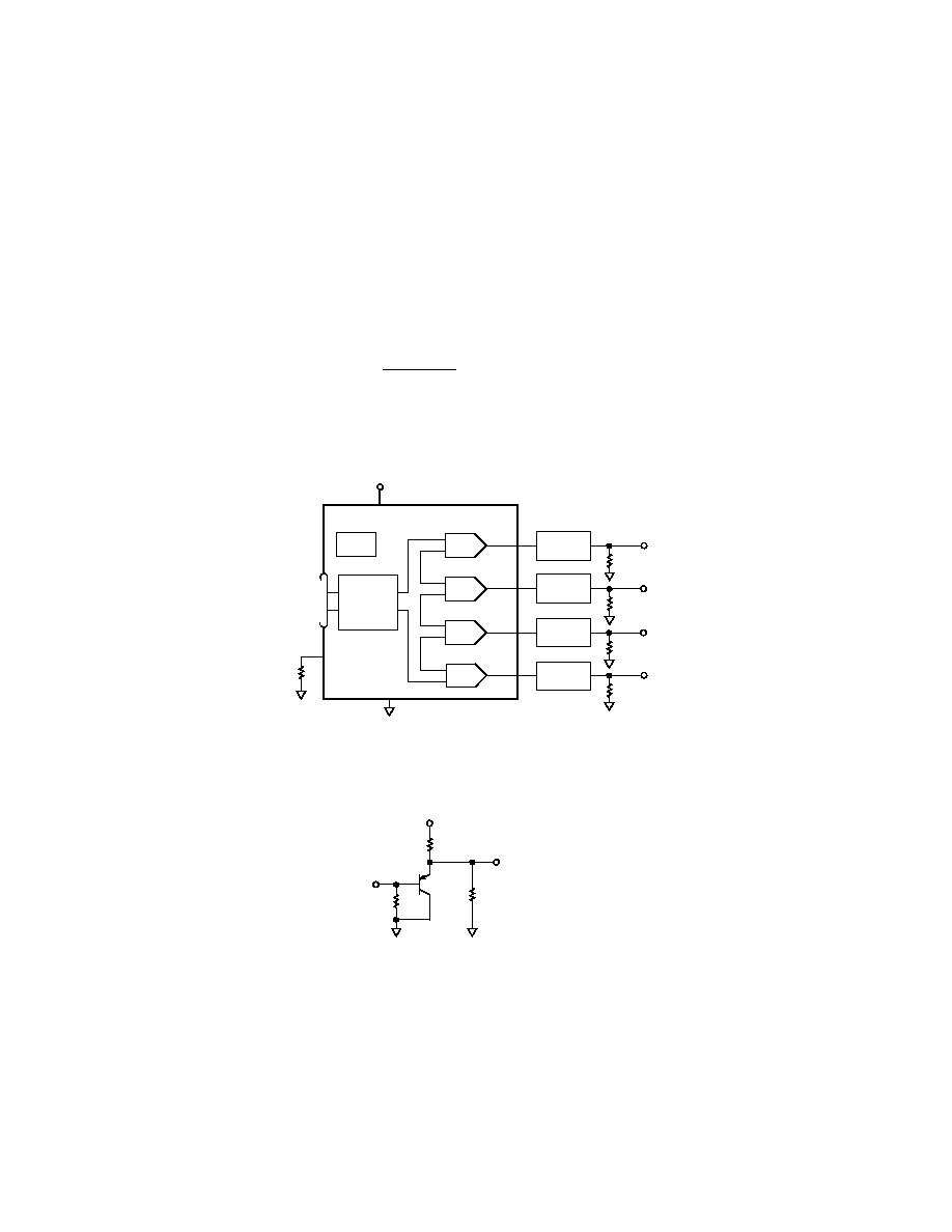
ADV7175A/ADV7176A
38
REV. B
For external buffering of the ADV7175A/ADV7176A DAC outputs, the configuration in Figure 71 is recommended. This configu-
ration shows the DAC outputs running at half (18 mA) their full current (36 mA) capability. This will allow the ADV7175A/ADV7176A
to dissipate less power, the analog current is reduced by 50% with a R
SET
of 300
and a R
LOAD
of 75
. This mode is recommended for
3.3 volt operation as optimum performance is obtained from the DAC outputs at 18 mA with a V
AA
of 3.3 volts. This buffer also
adds extra isolation on the video outputs, see buffer circuit in Figure 72. When calculating absolute output full current and voltage,
use the following equation:
V
OUT
=
I
OUT
×
R
LOAD
I
OUT
=
V
REF
×
K
(
)
R
SET
K
=
4.2146 constant , V
REF
=
1.235 V
ADV7175A/ADV7176A
V
REF
DIGITAL
CORE
PIXEL
PORT
300
R
SET
75
75
75
75
V
AA
OUTPUT
BUFFER
DAC A
OUTPUT
BUFFER
OUTPUT
BUFFER
OUTPUT
BUFFER
DAC C
DAC D
DAC B
Figure 71. Output DAC Buffering Configuration
2N2907
75
75
OUTPUT TO
TV/MONITOR
36
INPUT
V
CC
Figure 72. Recommended Output DAC Buffer
APPENDIX 7
OPTIONAL DAC BUFFERING
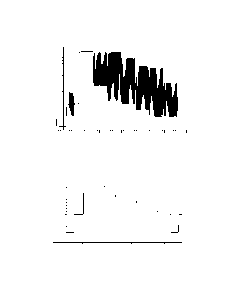
ADV7175A/ADV7176A
39
REV. B
APPENDIX 8
OUTPUT WAVEFORMS
0.6
0.4
0.2
0.0
0.2
L608
0.0
10.0
20.0
30.0
40.0
50.0
60.0
MICROSECONDS
NOISE REDUCTION: 0.00 dB
APL = 39.1%
PRECISION MODE OFF
SOUND-IN-SYNC OFF
625 LINE PAL
NO FILTERING
SYNCHRONOUS
SYNC = SOURCE
SLOW CLAMP TO 0.00 V AT 6.72 s
FRAMES SELECTED: 1 2 3 4
VOLTS
Figure 73. 100/ 75% PAL Color Bars
MICROSECONDS
APL NEEDS SYNC = SOURCE!
PRECISION MODE OFF
SOUND-IN-SYNC OFF
625 LINE PAL
NO FILTERING
SYNCHRONOUS
SYNC = A
SLOW CLAMP TO 0.00 V AT 6.72 s
FRAMES SELECTED: 1
0.5
0.0
L575
0.0
10.0
20.0
30.0
40.0
50.0
60.0
70.0
VOLTS
Figure 74. 100/ 75% PAL Color Bars Luminance
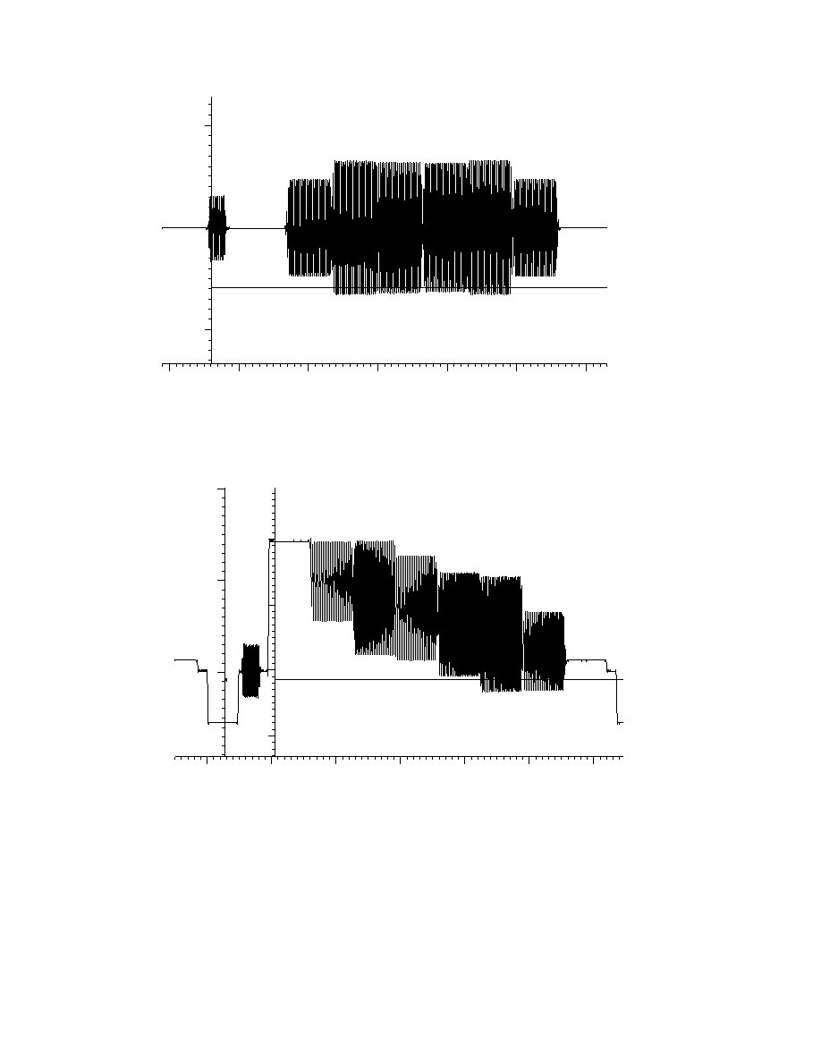
ADV7175A/ADV7176A
40
REV. B
APL NEEDS SYNC = SOURCE!
PRECISION MODE OFF
SOUND-IN-SYNC OFF
625 LINE PAL
NO FILTERING
SYNCHRONOUS
SYNC = A
SLOW CLAMP TO 0.00 V AT 6.72 s
FRAMES SELECTED: 1
0.5
0.0
0.5
10.0
30.0
40.0
50.0
60.0
20.0
MICROSECONDS
L575
VOLTS
NO BRUCH SIGNAL
Figure 75. 100/75% PAL Color Bars Chrominance
APL = 44.6%
PRECISION MODE OFF
525 LINE NTSC
NO FILTERING
SYNCHRONOUS
SYNC = A
SLOW CLAMP TO 0.00 V AT 6.72 s
FRAMES SELECTED: 1 2
MICROSECONDS
0.5
0.0
50.0
50.0
100.0
IRE:FLT
VOLTS
F1
L76
0.0
10.0
20.0
30.0
40.0
50.0
60.0
0.0
Figure 76. 100/75% NTSC Color Bars
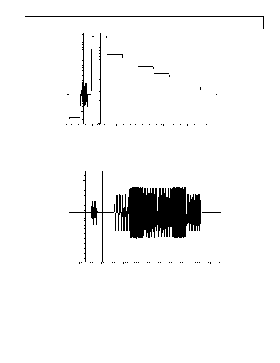
ADV7175A/ADV7176A
41
REV. B
NOISE REDUCTION: 15.05dB
APL = 44.7%
PRECISION MODE OFF
525 LINE NTSC
NO FILTERING
SYNCHRONOUS
SYNC = SOURCE
SLOW CLAMP TO 0.00 V AT 6.72 s
FRAMES SELECTED: 1 2
MICROSECONDS
10.0
20.0
30.0
40.0
50.0
60.0
0.6
0.4
0.2
0.0
0.2
50.0
0.0
IRE:FLT
VOLTS
F2
L238
Figure 77. 100/ 75% NTSC Color Bars Chrominance
NOISE REDUCTION: 15.05dB
APL NEEDS SYNC = SOURCE!
PRECISION MODE OFF
525 LINE NTSC
NO FILTERING
SYNCHRONOUS
SYNC = B
SLOW CLAMP TO 0.00 V AT 6.72 s
FRAMES SELECTED: 1 2
MICROSECONDS
0.0
10.0
20.0
30.0
40.0
50.0
60.0
0.4
0.2
0.0
0.2
0.4
VOLTS
50.0
50.0
F1
L76
IRE:FLT
Figure 78. 100/ 75% NTSC Color Bars Chrominance
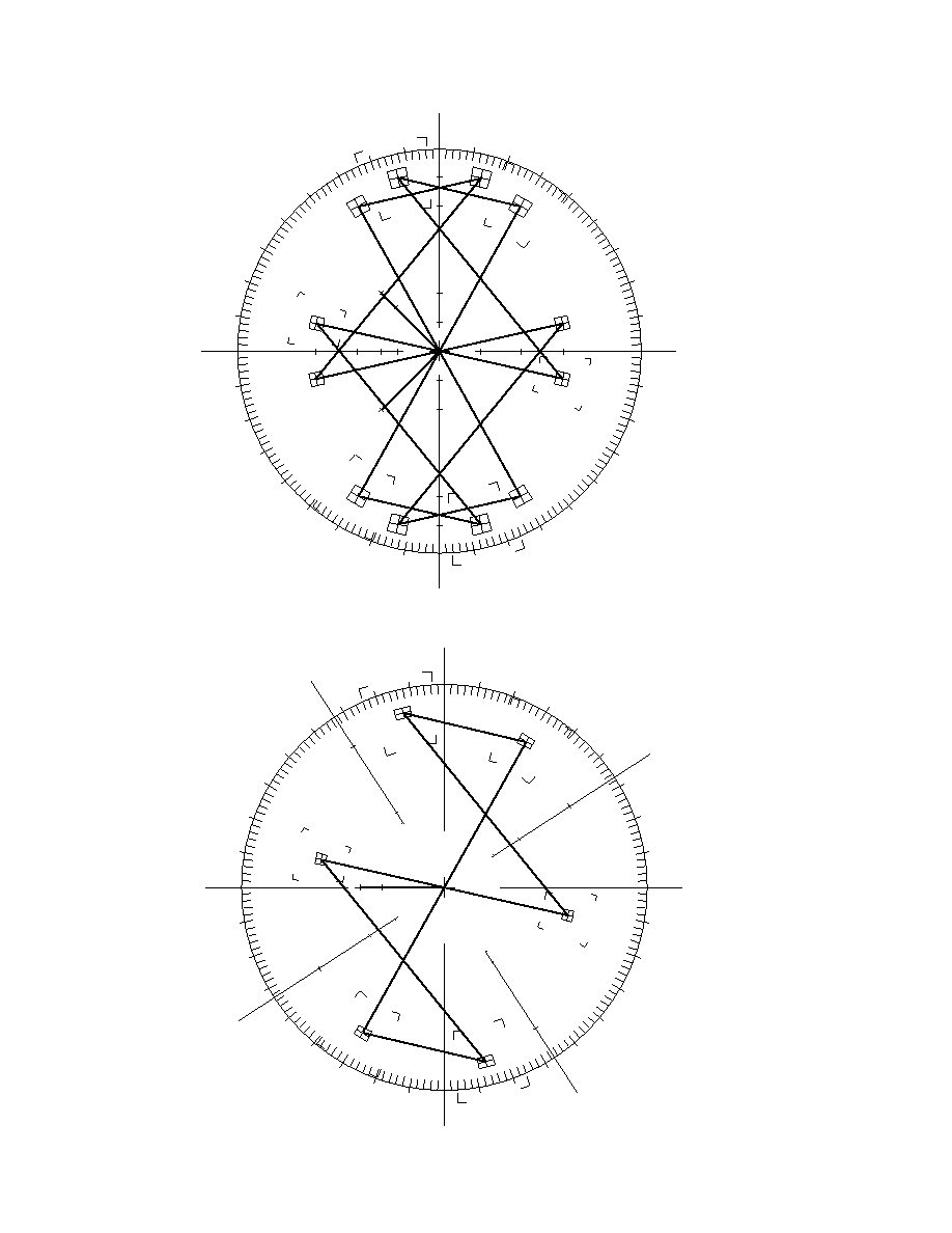
ADV7175A/ADV7176A
42
REV. B
APL = 39.6%
SOUND IN SYNC OFF
V
U
YI
yl
G
r
m
g
Cy
M
g
cy
g
R
75%
100%
b
B
SYSTEM LINE L608
ANGLE (DEG) 0.0
GAIN x 1.000 0.000dB
625 LINE PAL
BURST FROM SOURCE
DISPLAY +V & V
Figure 79. PAL Vector Plot
APL = 45.1%
SETUP 7.5%
R-Y
B-Y
YI
G
Cy
M
g
cy
I
R
75%
100%
b
B
SYSTEM LINE L76F1
ANGLE (DEG) 0.0
GAIN x 1.000 0.000dB
525 LINE NTSC
BURST FROM SOURCE
Q
Q
I
Figure 80. NTSC Vector Plot
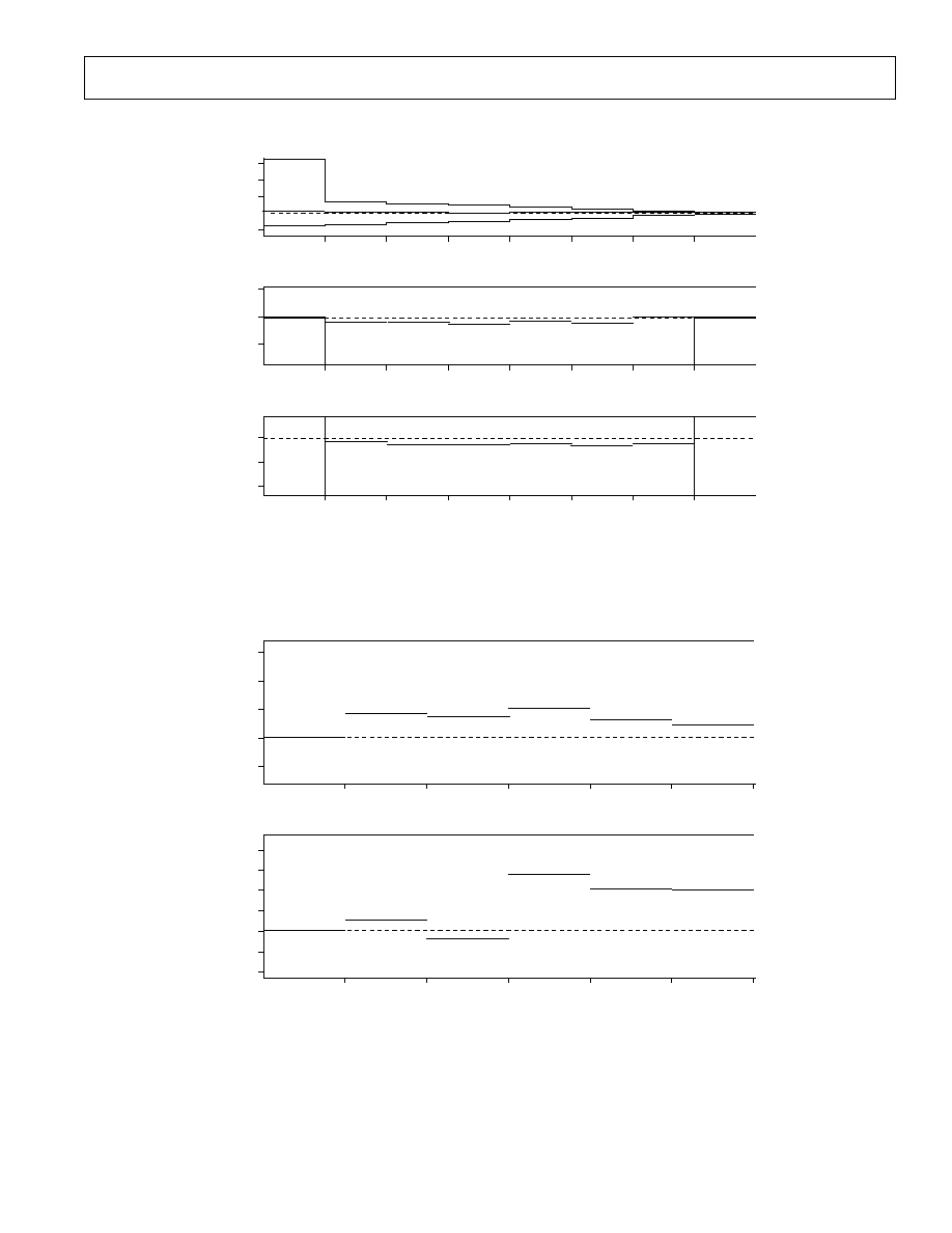
ADV7175A/ADV7176A
43
REV. B
COLOR BAR (NTSC)
WFM -->
FCC COLOR BAR
FIELD = 2 LINE = 28
LUMINANCE LEVEL (IRE)
0.4
0.2
0.2
0.0
0.2
0.1
0.2
0.1
0.0
0.2
0.2
0.3
0.2
0.3
0.0
0.0
. . . . .
0.1
0.2
0.2
0.1
0.3
0.2
- - - - -
CHROMINANCE LEVEL (IRE)
CHROMINANCE PHASE (DEG)
GRAY
YELLOW
CYAN
GREEN
MAGENTA
RED
BLUE
BLACK
AVERAGE:
32 --> 32
REFERENCE 75/7.5/75/7.5 COLOR BAR STANDARD
30.0
20.0
10.0
0.0
10.0
1.0
0.0
1.0
0.0
1.0
2.0
Figure 81. NTSC Color Bar Measurement
DGDP (NTSC)
WFM -->
MOD 5 STEP
BLOCK MODE START F2 L64, STEP = 32, END = 192
DIFFERENTIAL GAIN (%)
MIN = 0.00 MAX = 0.11 p-p/MAX = 0.11
0.00
0.08
0.07
0.11
0.07
0.05
0.3
0.2
0.1
0.0
0.1
0.20
0.15
0.10
0.05
0.00
0.05
0.10
0.00
0.03
0.02
0.14
0.10
0.10
DIFFERENTIAL PHASE (DEG)
MIN = 0.02 MAX = 0.14 pk-pk = 0.16
1ST
2ND
3RD
4TH
5TH
6TH
Figure 82. NTSC Differential Gain and Phase Measurement
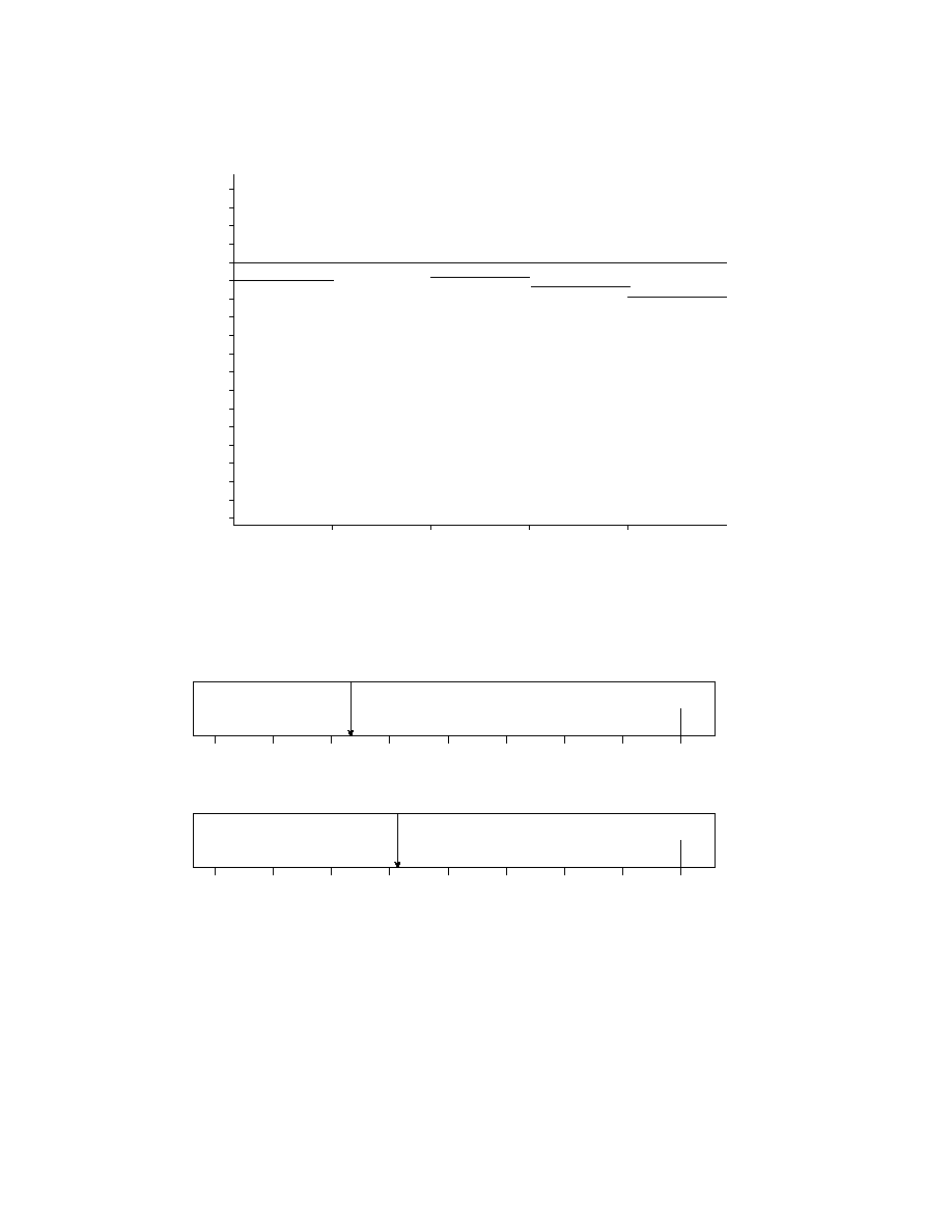
ADV7175A/ADV7176A
44
REV. B
LUMINANCE NONLINEARITY (NTSC)
WFM -->
5 STEP
FIELD = 2 LINE = 21
LUMINANCE NONLINEARITY (%)
pk-pk = 0.2
99.9
100.0
99.9
99.9
99.8
100.4
100.3
100.2
100.1
100.0
99.9
99.8
99.7
99.6
99.5
99.4
99.3
99.2
99.1
99.0
98.9
98.8
98.7
98.6
1ST
2ND
3RD
4TH
5TH
Figure 83. NTSC Luminance Nonlinearity Measurement
CHROMINANCE AM PM (NTSC)
WFM -->
APPROPRIATE
FULL FIELD (BOTH FIELDS)
BANDWIDTH 100Hz TO 500kHz
75.0
AM NOISE
68.4dB RMS
70.0
65.0
60.0
55.0
50.0
45.0
40.0
dB RMS
75.0
PM NOISE
64.4dB RMS
70.0
65.0
60.0
55.0
50.0
45.0
40.0
dB RMS
(0dB = 714mV p-p WITH AGC FOR 100% CHROMINANCE LEVEL)
Figure 84. NTSC AMPM Noise Measurement
ADV7175A/ADV7176A
45
REV. B
NOISE SPECTRUM (NTSC)
WFM -->
PEDESTAL
FIELD = 2 LINE = 64
AMPLITUDE (0 dB = 714mV p-p)
NOISE LEVEL = 80.1 dB RMS
BANDWIDTH 100kHz TO FULL
5.0
10.0
15.0
20.0
25.0
30.0
35.0
40.0
45.0
50.0
55.0
60.0
65.0
70.0
75.0
80.0
85.0
90.0
95.0
100.0
1.0
2.0
3.0
4.0
5.0
6.0
MHz
Figure 85. NTSC SNR Pedestal Measurement
NOISE SPECTRUM (NTSC)
WFM -->
RAMP SIGNAL
FIELD = 2 LINE = 64
AMPLITUDE (0 dB = 714mV p-p)
NOISE LEVEL = 61.7 dB RMS
BANDWIDTH 10kHz TO FULL (TILT NULL)
5.0
10.0
15.0
20.0
25.0
30.0
35.0
40.0
45.0
50.0
55.0
60.0
65.0
70.0
75.0
80.0
85.0
90.0
95.0
100.0
1.0
2.0
3.0
4.0
5.0
MHz
Figure 86. NTSC SNR Ramp Measurement
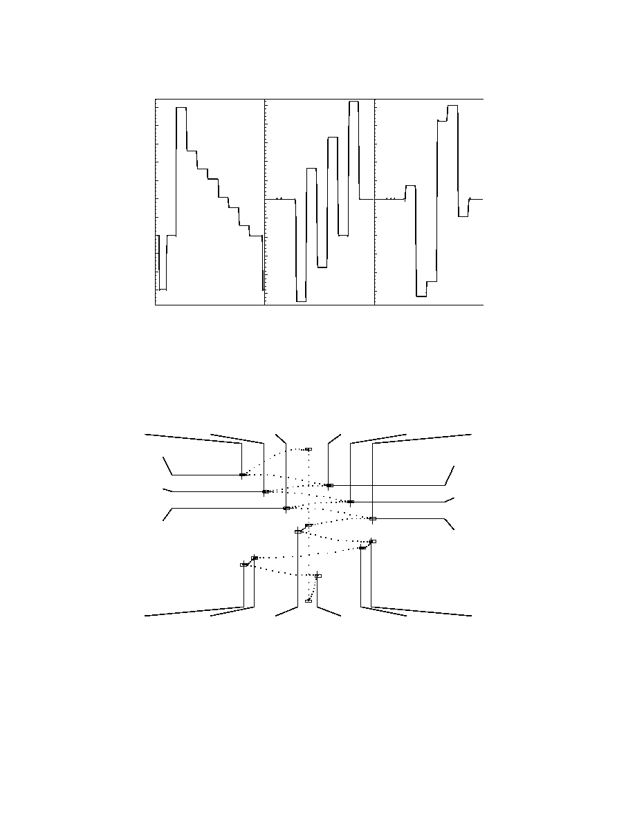
ADV7175A/ADV7176A
46
REV. B
PARADE SMPTE/EBU PAL
mV
Y(A)
mV
Pb(B)
mV
Pr(C)
700
600
500
400
300
200
100
0
100
200
300
250
200
150
100
50
50
100
150
200
250
0
250
200
150
100
50
50
100
150
200
250
0
Figure 87. PAL YUV Parade Plot
LIGHTNING
COLORBARS: 75% SMPTE/EBU (50Hz)
AVERAGE 15 --> 32
L183
Pk-WHITE (100%) 700.0mV SETUP 0.0% COLOR Pk-Pk 525.0mV
VM700A DEV 3 WC TEMP = 90 C V
DD
= 5.25V
CHANNEL C SYSTEM DEFAULT
10-APR-97
09:23:07
YI
274.82
0.93%
G
173.24
0.19%
R
88.36
0.19%
CY
88.31
0.28%
M
174.35
0.65%
B
260.51
0.14%
YI
462.80
0.50%
G
307.54
0.21%
R
156.63
0.22%
B-Y
W
YI
G
R
B
G
CY
R-Y
W
YI
M
R
CY
262.17
0.13%
G
218.70
0.51%
B
42.54
0.69%
YI
41.32
0.76%
M
212.28
3.43%
R
252.74
3.72%
CY
864.78
0.88%
M
216.12
0.33%
B
61.00
1.92%
CY
M
B
COLOR Pk-Pk: B-Y 532.33mV
1.40%
R-Y 514.90mV 1.92%
Pk-WHITE: 700.4mV (100%) SETUP 0.01%
DELAY: B-Y 6ns R-Y 6ns
Figure 88. PAL YUV Lighting Plot
ADV7175A/ADV7176A
47
REV. B
COMPONENT NOISE
LINE = 202
AMPLITUDE (0dB = 700mV p-p)
NOISE dB RMS
BANDWIDTH 10kHz TO 5.0MHz
5.0
10.0
15.0
20.0
25.0
30.0
35.0
40.0
45.0
50.0
55.0
60.0
65.0
70.0
75.0
80.0
85.0
90.0
95.0
100.0
1.0
2.0
3.0
4.0
5.0
MHz
5.0
0.0
-->Y 82.1
Pb 82.3
Pr 83.3
Figure 89. PAL YUV SNR Plot
COMPONENT MULTIBURST
LINE = 202
AMPLITUDE (0dB = 100% OF 688.1mV 683.4mV 668.9mV
0.04
0.02
0.05
0.68
2.58
8.05
(dB)
0.49
0.99
2.00
3.99
4.79
5.79
0.49
0.99
1.99
2.39
2.89
0.49
0.99
1.99
2.39
2.89
0.0
5.0
10.0
Y
0.0
5.0
10.0
Pb
0.0
5.0
10.0
Pr
(MHz)
0.21
0.23
0.78
2.59
7.15
0.25
0.25
0.77
2.59
7.13
Figure 90. PAL YUV Multiburst Response
ADV7175A/ADV7176A
48
REV. B
R
M
g
YI
BK
B
G
CY
COMPONENT VECTOR SMPTE/EBU, 75%
Figure 91. PAL YUV Vector Plot
RGB PARADE SMPTE/EBU
mV
GREEN (A)
mV
BLUE (B)
mV
RED (C)
700
600
500
400
300
200
100
0
100
200
300
700
600
500
400
300
200
100
0
700
600
500
400
300
200
100
0
100
200
300
100
200
300
20 --> 32
Figure 92. PAL RGB Waveforms

ADV7175A/ADV7176A
49
REV. B
INDEX
Contents
Page No.
GENERAL DESCRIPTION . . . . . . . . . . . . . . . . . . . . . . . . 1
ADV7175A/ADV7176A SPECIFICATIONS . . . . . . . . . . . 2
TIMING SPECIFICATIONS . . . . . . . . . . . . . . . . . . . . . . 6
ABSOLUTE MAXIMUM RATINGS . . . . . . . . . . . . . . . . 9
ORDERING GUIDE . . . . . . . . . . . . . . . . . . . . . . . . . . . . . 9
PIN CONFIGURATION . . . . . . . . . . . . . . . . . . . . . . . . . . 9
PIN FUNCTION DESCRIPTIONS . . . . . . . . . . . . . . . . 10
DATA PATH DESCRIPTION . . . . . . . . . . . . . . . . . . . . 11
INTERNAL FILTER RESPONSE . . . . . . . . . . . . . . . . . . 11
COLOR BAR GENERATION . . . . . . . . . . . . . . . . . . . . . 13
SQUARE PIXEL MODE . . . . . . . . . . . . . . . . . . . . . . . . . 13
COLOR SIGNAL CONTROL . . . . . . . . . . . . . . . . . . . . . 13
BURST SIGNAL CONTROL . . . . . . . . . . . . . . . . . . . . . 13
NTSC PEDESTAL CONTROL . . . . . . . . . . . . . . . . . . . . 13
PIXEL TIMING DESCRIPTION . . . . . . . . . . . . . . . . . . 13
SUBCARRIER RESET . . . . . . . . . . . . . . . . . . . . . . . . . . . 13
REAL TIME CONTROL . . . . . . . . . . . . . . . . . . . . . . . . . 13
VIDEO TIMING DESCRIPTION . . . . . . . . . . . . . . . . . . 13
Timing Mode 0 . . . . . . . . . . . . . . . . . . . . . . . . . . . . . . . . 14
Timing Mode 1 . . . . . . . . . . . . . . . . . . . . . . . . . . . . . . . . 16
Timing Mode 2 . . . . . . . . . . . . . . . . . . . . . . . . . . . . . . . . 18
Timing Mode 3 . . . . . . . . . . . . . . . . . . . . . . . . . . . . . . . . 20
OUTPUT VIDEO TIMING . . . . . . . . . . . . . . . . . . . . . . . 21
POWER-ON RESET . . . . . . . . . . . . . . . . . . . . . . . . . . . . 21
MPU PORT DESCRIPTION . . . . . . . . . . . . . . . . . . . . . . 21
REGISTER ACCESSES . . . . . . . . . . . . . . . . . . . . . . . . . . 23
REGISTER PROGRAMMING . . . . . . . . . . . . . . . . . . . . 23
MODE REGISTER 0 . . . . . . . . . . . . . . . . . . . . . . . . . . . . 23
MR0 BIT DESCRIPTION . . . . . . . . . . . . . . . . . . . . . . . . 23
Contents
Page No.
MODE REGISTER 1 . . . . . . . . . . . . . . . . . . . . . . . . . . . . 24
MR1 BIT DESCRIPTION . . . . . . . . . . . . . . . . . . . . . . . . 24
SUBCARRIER FREQUENCY REGISTER . . . . . . . . . . . 24
SUBCARRIER PHASE REGISTER . . . . . . . . . . . . . . . . . 24
TIMING REGISTER 0 . . . . . . . . . . . . . . . . . . . . . . . . . . 24
TR0 BIT DESCRIPTION . . . . . . . . . . . . . . . . . . . . . . . . 24
CLOSED CAPTIONING EVEN FIELD . . . . . . . . . . . . . 25
CLOSED CAPTIONING ODD FIELD . . . . . . . . . . . . . 25
TIMING REGISTER 1 . . . . . . . . . . . . . . . . . . . . . . . . . . 25
TR1 BIT DESCRIPTION . . . . . . . . . . . . . . . . . . . . . . . . 25
MODE REGISTER 2 . . . . . . . . . . . . . . . . . . . . . . . . . . . . 25
MR2 BIT DESCRIPTION . . . . . . . . . . . . . . . . . . . . . . . . 25
NTSC PEDESTAL/PAL TELETEXT CONTROL
REGISTERS 30 . . . . . . . . . . . . . . . . . . . . . . . . . . . . . . 26
MODE REGISTER 3 . . . . . . . . . . . . . . . . . . . . . . . . . . . . 26
MR3 BIT DESCRIPTION . . . . . . . . . . . . . . . . . . . . . . . . 26
TELETEXT CONTROL REGISTER TC07 . . . . . . . . . . 27
APPENDIX 1. BOARD DESIGN AND LAYOUT
CONSIDERATIONS . . . . . . . . . . . . . . . . . . . . . . . . . . . 28
APPENDIX 2. CLOSED CAPTIONING . . . . . . . . . . . . 30
APPENDIX 3. TELETEXT INSERTION . . . . . . . . . . . 31
APPENDIX 4. WAVEFORMS . . . . . . . . . . . . . . . . . . . . 32
APPENDIX 5. REGISTER VALUES . . . . . . . . . . . . . . . 36
APPENDIX 6. OPTIONAL OUTPUT FILTER . . . . . . . 37
APPENDIX 7. OPTIONAL DAC BUFFERING . . . . . . 38
APPENDIX 8. OUTPUT WAVEFORMS . . . . . . . . . . . . 39
OUTLINE DIMENSIONS . . . . . . . . . . . . . . . . . . . . . . . . 50
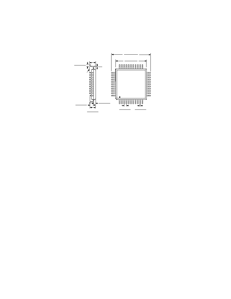
ADV7175A/ADV7176A
50
REV. B
OUTLINE DIMENSIONS
Dimensions shown in inches and (mm).
Plastic Quad Flatpack
(S-44)
0.548 (13.925)
0.546 (13.875)
TOP VIEW
(PINS DOWN)
1
33
34
44
11
12
23
22
0.033 (0.84)
0.029 (0.74)
0.398 (10.11)
0.390 (9.91)
0.016 (0.41)
0.012 (0.30)
0.083 (2.11)
0.077 (1.96)
0.040 (1.02)
0.032 (0.81)
0.040 (1.02)
0.032 (0.81)
SEATING
PLANE
0.096 (2.44)
MAX
0.037 (0.94)
0.025 (0.64)
8
°
0.8
°

51

52
C3184a01/98
PRINTED IN U.S.A.