/home/web/htmldatasheet/RUSSIAN/html/ad/211097
REV. A
Information furnished by Analog Devices is believed to be accurate and
reliable. However, no responsibility is assumed by Analog Devices for its
use, nor for any infringements of patents or other rights of third parties
which may result from its use. No license is granted by implication or
otherwise under any patent or patent rights of Analog Devices.
a
ADV7177/ADV7178*
One Technology Way, P.O. Box 9106, Norwood, MA 02062-9106, U.S.A.
Tel: 781/329-4700
World Wide Web Site: http://www.analog.com
Fax: 781/326-8703
© Analog Devices, Inc., 2001
Integrated Digital CCIR-601
to PAL/NTSC Video Encoder
FEATURES
ITU-R BT601/656 YCrCb to PAL/NTSC Video Encoder
High Quality 9-Bit Video DACs
Integral Nonlinearity <1 LSB at 9 Bits
NTSC-M, PAL-M/N, PAL-B/D/G/H/I
Single 27 MHz Crystal/Clock Required ( 2 Oversampling)
75 dB Video SNR
32-Bit Direct Digital Synthesizer for Color Subcarrier
Multistandard Video Output Support:
Composite (CVBS)
Component S-Video (Y/C)
Component YUV or RGB
Video Input Data Port Supports:
CCIR-656 4:2:2 8-Bit Parallel Input Format
4:2:2 16-Bit Parallel Input Format
Full Video Output Drive or Low Signal Drive Capability
34.7 mA max into 37.5 (Doubly-Terminated 75R)
5 mA min with External Buffers
Programmable Simultaneous Composite and S-VHS
(VHS) Y/C or RGB (SCART)/YUV Video Outputs
Programmable Luma Filters (Low-Pass/Notch/Extended)
Programmable VBI (Vertical Blanking Interval)
Programmable Subcarrier Frequency and Phase
Programmable LUMA Delay
Individual ON/OFF Control of Each DAC
CCIR and Square Pixel Operation
Color Signal Control/Burst Signal Control
Interlaced/Noninterlaced Operation
Complete On-Chip Video Timing Generator
OSD Support (AD7177 Only)
Programmable Multimode Master/Slave Operation
Macrovision AntiTaping Rev 7.01 (ADV7178 Only)**
Closed Captioning Support
Onboard Voltage Reference
2-Wire Serial MPU Interface (I
2
C
®
-Compatible)
Single Supply 5 V or 3 V Operation
Small 44-Lead PQFP Package
Synchronous 27 MHz/13.5 MHz Clock O/P
APPLICATIONS
MPEG-1 and MPEG-2 Video, DVD, Digital Satellite/
Cable Systems (Set Top Boxes/IRDs), Digital TVs,
CD Video/Karaoke, Video Games, PC Video/Multimedia
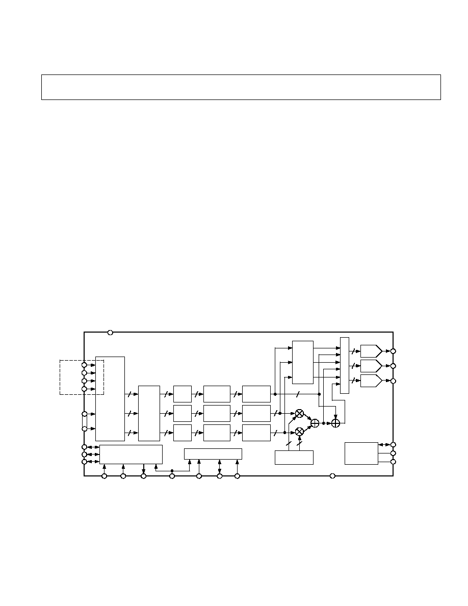
GENERAL DESCRIPTION
The ADV7177/ADV7178 is an integrated digital video encoder
that converts Digital CCIR-601 4:2:2 8- or 16-bit component
video data into a standard analog baseband television signal
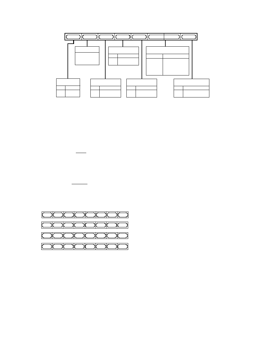
FUNCTIONAL BLOCK DIAGRAM
OSD_EN
OSD_0
OSD_1
OSD_2
P7P0
P15P8
COLOR
DATA
ADV7177
ONLY
4:2:2 TO
4:4:4
INTER-
POLATOR
8
8
8
8
ADD
BURST
8
INTER-
POLATOR
8
V
LOW-PASS
FILTER
9
9
9
9
9
SIN/COS
DDS BLOCK
YUV TO
RBG
MATRIX
M
U
L
T
I
P
L
E
X
E
R
9
9
9
9-BIT
DAC
9-BIT
DAC
9-BIT
DAC
DAC C (PIN 26)
DAC B (PIN 27)
DAC A (PIN 31)
ADV7177/ADV7178
VOLTAGE
REFERENCE
CIRCUIT
VIDEO TIMING
GENERATOR
I
2
C MPU PORT
CLOCK
CLOCK CLOCK/2
RESET
SCLOCK SDATA ALSB
GND
V
REF
R
SET
COMP
V
AA
HSYNC
FIELD/
VSYNC
BLANK
8
ADD
BURST
8
INTER-
POLATOR
8
U
LOW-PASS
FILTER
8
ADD
SYNC
8
INTER-
POLATOR
8
Y
LOW-PASS
FILTER
YCrCb
TO
YUV
MATRIX
*Protected by U.S. Patent Numbers 5,343,196 and 5,442,355 and other intellectual property rights.
**This device is protected by U.S. Patent Numbers 4,631,603, 4,577,216, 4,819,098 and other intellectual property rights. The Macrovision anticopy process is
licensed for noncommercial home use only, which is its sole intended use in the device. Please contact sales office for latest Macrovision version available.
NOTE: ITU-R and CCIR are used interchangeably in this document (ITU-R has replaced CCIR recommendations).
I
2
C is a registered trademark of Philips Corporation.
(Continued on page 11)

2
REV. A
ADV7177/ADV7178SPECIFICATIONS
(V
AA
= 5 V 5%
1
, V
REF
= 1.235 V, R
SET
= 300
. All specifications T
MIN
to T
MAX
2
unless otherwise noted.)
Parameter
Conditions
1
Min
Typ
Max
Unit
STATIC PERFORMANCE
3
Resolution (Each DAC)
9
Bits
Accuracy (Each DAC)
Integral Nonlinearity
±1.0
LSB
Differential Nonlinearity
Guaranteed Monotonic
±1.0
LSB
DIGITAL INPUTS
3
Input High Voltage, V
INH
2
V
Input Low Voltage, V
INL
0.8
V
Input Current, I
IN
4
V
IN
= 0.4 V or 2.4 V
±1
µA
Input Current, I
IN
5
V
IN
= 0.4 V or 2.4 V
±50
µA
Input Capacitance, C
IN
10
pF
DIGITAL OUTPUTS
3
Output High Voltage, V
OH
I
SOURCE
= 400
µA
2.4
V
Output Low Voltage, V
OL
I
SINK
= 3.2 mA
0.4
V
Three-State Leakage Current
10
µA
Three-State Output Capacitance
10
pF
ANALOG OUTPUTS
3
Output Current
6
R
SET
= 300
, R
L
= 75
16.5
17.35
18.5
mA
Output Current
7
5
mA
DAC-to-DAC Matching
0.6
5
%
Output Compliance, V
OC
0
1.4
V
Output Impedance, R
OUT
15
k
Output Capacitance, C
OUT
I
OUT
= 0 mA
30
pF
VOLTAGE REFERENCE
3
Reference Range, V
REF
I
VREFOUT
= 20
µA
1.112
1.235
1.359
V
POWER REQUIREMENTS
3, 8
V
AA
4.75
5.0
5.25
V
Low Power Mode
I
DAC
(max)
9
62
mA
I
DAC
(min)
9
25
mA
I
CCT
10
100
150
mA
Power Supply Rejection Ratio
COMP = 0.1
µF
0.01
0.5
%/%
NOTES
1
1
The max/min specifications are guaranteed over this range. The max/min values are typical over 4.75 V to 5.25 V.
1
2
Temperature range T
MIN
to T
MAX
: 0
°C to 70°C.
1
3
Guaranteed by characterization.
1
4
All digital input pins except pins
RESET, OSD0 and CLOCK.
1
5
Excluding all digital input pins except pins
RESET, OSD0 and CLOCK.
1
6
Full
drive into 75
load.
1
7
Minimum drive current (used with buffered/scaled output load).
1
8
Power measurements are taken with Clock Frequency = 27 MHz. Max T
J
= 110
°C.
1
9
I
DAC
is the total current (min corresponds to 5 mA output per DAC, max corresponds to 18.5 mA output per DAC) to drive all three DACs. Turning off individual
DACs reduces I
DAC
correspondingly.
10
I
CCT
(Circuit Current) is the continuous current required to drive the device.
Specifications subject to change without notice.
5 V SPECIFICATIONS

3
REV. A
ADV7177/ADV7178
Parameter
Conditions
1
Min
Typ
Max
Unit
STATIC PERFORMANCE
3
Resolution (Each DAC)
9
Bits
Accuracy (Each DAC)
Integral Nonlinearity
±0.5
LSB
Differential Nonlinearity
Guaranteed Monotonic
±0.5
LSB
DIGITAL INPUTS
Input High Voltage, V
INH
2
V
Input Low Voltage, V
INL
0.8
V
Input Current, I
IN
3, 4
V
IN
= 0.4 V or 2.4 V
±1
µA
Input Current, I
IN
3,
5
V
IN
= 0.4 V or 2.4 V
±50
µA
Input Capacitance, C
IN
10
pF
DIGITAL OUTPUTS
Output High Voltage, V
OH
I
SOURCE
= 400
µA
2.4
V
Output Low Voltage, V
OL
I
SINK
= 3.2 mA
0.4
V
Three-State Leakage Current
3
10
µA
Three-State Output Capacitance
3
10
pF
ANALOG OUTPUTS
3
Output Current
6, 7
R
SET
= 300
, R
L
= 75
16.5
17.35
18.5
mA
Output Current
8
5
mA
DAC-to-DAC Matching
2.0
%
Output Compliance, V
OC
0
1.4
V
Output Impedance, R
OUT
15
k
Output Capacitance, C
OUT
I
OUT
= 0 mA
30
pF
POWER REQUIREMENTS
3, 9
V
AA
3.0
3.3
3.6
V
Normal Power Mode
I
DAC
(max)
10
R
SET
= 300
, R
L
= 150
113
116
mA
I
DAC
(min)
10
15
mA
I
CCT
9
45
mA
Low Power Mode
I
DAC
(max)
10
60
mA
I
DAC
(min)
10
25
mA
I
CCT
11
45
mA
Power Supply Rejection Ratio
COMP = 0.1
µF
0.01
0.5
%/%
NOTES
1
1
The max/min specifications are guaranteed over this range. The max/min values are typical over 3.0 V to 3.6 V.
1
2
Temperature range T
MIN
to T
MAX
: 0
°C to 70°C.
1
3
Guaranteed by characterization.
1
4
All digital input pins except pins
RESET, OSD0 and CLOCK.
1
5
Excluding all digital input pins except pins
RESET, OSD0 and CLOCK.
1
6
Full
drive into 75
load.
1
7
DACs can output 35 mA typically at 3.3 V (R
SET
= 150
and R
L
= 75
), optimum performance obtained at 18 mA DAC current (R
SET
= 300
and R
L
= 150
).
1
8
Minimum drive current (used with buffered/scaled output load).
1
9
Power measurements are taken with Clock Frequency = 27 MHz. Max T
J
= 110
°C.
10
I
DAC
is the total current (min corresponds to 5 mA output per DAC, max corresponds to 38 mA output per DAC) to drive all three DACs. Turning off individual
DACs reduces I
DAC
correspondingly.
11
I
CCT
(Circuit Current) is the continuous current required to drive the device.
Specifications subject to change without notice.
3.3 V SPECIFICATIONS
(V
AA
= 3.0 V3.6 V
1
, V
REF
= 1.235 V, R
SET
= 300 . All specifications T
MIN
to T
MAX
2
unless otherwise noted.)

4
REV. A
ADV7177/ADV7178SPECIFICATIONS
Parameter
Conditions
1
Min
Typ
Max
Unit
Filter Characteristics
Luma Bandwidth
3
(Low-Pass Filter)
NTSC Mode
Stopband Cutoff
>54 dB Attenuation
7.0
MHz
Passband Cutoff F
3 dB
>3 dB Attenuation
4.2
MHz
Chroma Bandwidth
NTSC Mode
Stopband Cutoff
>40 dB Attenuation
3.2
MHz
Passband Cutoff F
3 dB
>3 dB Attenuation
2.0
MHz
Luma Bandwidth
3
(Low-Pass Filter)
PAL MODE
Stopband Cutoff
>50 dB Attenuation
7.4
MHz
Passband Cutoff F
3 dB
>3 dB Attenuation
5.0
MHz
Chroma Bandwidth
PAL MODE
Stopband Cutoff
>40 dB Attenuation
4.0
MHz
Passband Cutoff F
3 dB
>3 dB Attenuation
2.4
MHz
Differential Gain
4
Lower Power Mode
2.0
%
Differential Phase
4
Lower Power Mode
1.5
Degrees
SNR
4
(Pedestal)
RMS
75
dB rms
Peak Periodic
70
dB p-p
SNR
4
(Ramp)
RMS
57
dB rms
Peak Periodic
56
dB p-p
Hue Accuracy
4
1.2
Degrees
Color Saturation Accuracy
4
1.4
%
Chroma Nonlinear Gain
4
Referenced to 40 IRE
1.0
±%
Chroma Nonlinear Phase
4
NTSC
0.4
±Degrees
PAL
0.6
±Degrees
Chroma/Luma Intermod
4
Referenced to 714 mV (NTSC)
0.2
±%
Referenced to 700 mV (PAL)
0.2
±%
Chroma/Luma Gain Ineq
4
0.6
±%
Chroma/Luma Delay Ineq
4
2.0
ns
Luminance Nonlinearity
4
1.2
±%
Chroma AM Noise
4
64
dB
Chroma PM Noise
4
62
dB
NOTES
1
The max/min specifications are guaranteed over this range. The max/min values are typical over 4.75 V to 5.25 V.
2
Temperature range T
MIN
to T
MAX
: 0
°C to 70°C.
3
These specifications are for the low-pass filter only and guaranteed by design. For other internal filters, see Figure 5.
4
Guaranteed by characterization.
Specifications subject to change without notice.
5 V DYNAMIC SPECIFICATIONS
1
(V
AA
= 4.75 V5.25 V
1
, V
REF
= 1.235 V, R
SET
= 300
. All specifications T
MIN
to T
MAX
2
unless otherwise noted.)

5
REV. A
ADV7177/ADV7178
Parameter
Conditions
1
Min
Typ
Max
Unit
Filter Characteristics
Luma Bandwidth
3
(Low-Pass Filter)
NTSC Mode
Stopband Cutoff
>54 dB Attenuation
7.0
MHz
Passband Cutoff F
3 dB
>3 dB Attenuation
4.2
MHz
Chroma Bandwidth
NTSC Mode
Stopband Cutoff
>40 dB Attenuation
3.2
MHz
Passband Cutoff F
3 dB
>3 dB Attenuation
2.0
MHz
Luma Bandwidth
3
(Low-Pass Filter)
PAL MODE
Stopband Cutoff
>50 dB Attenuation
7.4
MHz
Passband Cutoff F
3 dB
>3 dB Attenuation
5.0
MHz
Chroma Bandwidth
PAL MODE
Stopband Cutoff
>40 dB Attenuation
4.0
MHz
Passband Cutoff F
3 dB
>3 dB Attenuation
2.4
MHz
Differential Gain
4
Normal Power Mode
1.0
%
Differential Phase
4
Normal Power Mode
1.0
Degrees
SNR
4
(Pedestal)
RMS
70
dB rms
Peak Periodic
64
dB p-p
SNR
4
(Ramp)
RMS
56
dB rms
Peak Periodic
54
dB p-p
Hue Accuracy
4
1.2
Degrees
Color Saturation Accuracy
4
1.4
%
Luminance Nonlinearity
4
1.4
±%
Chroma AM Noise
4
NTSC
64
dB
Chroma PM Noise
4
NTSC
62
dB
Chroma AM Noise
4
PAL
64
dB
Chroma PM Noise
4
PAL
62
dB
NOTES
1
The max/min specifications are guaranteed over this range. The max/min values are typical over 3.0 V to 3.6 V.
2
Temperature range T
MIN
to T
MAX
: 0
°C to 70°C.
3
These specifications are for the low-pass filter only and guaranteed by design. For other internal filters, see Figure 5.
4
Guaranteed by characterization.
Specifications subject to change without notice.
3.3 V DYNAMIC SPECIFICATIONS
1
(V
AA
= 3.0 V3.6 V
1
, V
REF
= 1.235 V, R
SET
= 300
. All specifications T
MIN
to T
MAX
2
unless otherwise noted.)

ADV7177/ADV7178
6
REV. A
5 V TIMING SPECIFICATIONS
(V
AA
= 4.75 V5.25 V
1
, V
REF
= 1.235 V, R
SET
= 300
. All specifications T
MIN
to T
MAX
2
unless
otherwise noted.)
Parameter
Conditions
Min
Typ
Max
Unit
MPU PORT
3, 4
SCLOCK Frequency
0
100
kHz
SCLOCK High Pulsewidth, t
1
4.0
µs
SCLOCK Low Pulsewidth, t
2
4.7
µs
Hold Time (Start Condition), t
3
After This Period the First Clock Is Generated
4.0
µs
Setup Time (Start Condition), t
4
Relevant for Repeated Start Condition
4.7
µs
Data Setup Time, t
5
250
ns
SDATA, SCLOCK Rise Time, t
6
1
µs
SDATA, SCLOCK Fall Time, t
7
300
ns
Setup Time (Stop Condition), t
8
4.7
µs
ANALOG OUTPUTS
3, 5
Analog Output Delay
5
ns
DAC Analog Output Skew
0
ns
CLOCK CONTROL
AND PIXEL PORT
3, 6
f
CLOCK
27
MHz
Clock High Time, t
9
8
ns
Clock Low Time, t
10
8
ns
Data Setup Time, t
11
3.5
ns
Data Hold Time, t
12
4
ns
Control Setup Time, t
11
4
ns
Control Hold Time, t
12
3
ns
Digital Output Access Time, t
13
24
ns
Digital Output Hold Time, t
14
4
ns
Pipeline Delay, t
15
37
Clock Cycles
RESET CONTROL
3, 4
RESET Low Time
6
ns
INTERNAL CLOCK CONTROL
Clock/2 Rise Time, t
16
7
ns
Clock/2 Fall Time, t
17
7
ns
OSD TIMING
4
OSD Setup Time, t
18
6
ns
OSD Hold Time, t
19
2
ns
NOTES
1
The max/min specifications are guaranteed over this range.
2
Temperature range T
MIN
to T
MAX
: 0
°C to 70°C.
3
TTL input values are 0 to 3 volts, with input rise/fall times
3 ns, measured between the 10% and 90% points. Timing reference points at 50% for inputs and
outputs. Analog output load
10 pF.
4
Guaranteed by characterization.
5
Output delay measured from the 50% point of the rising edge of CLOCK to the 50% point of full-scale transition.
6
Pixel Port consists of the following:
Pixel Inputs:
P15P0
Pixel Controls:
HSYNC, FIELD/VSYNC, BLANK
Clock Input:
CLOCK
Specifications subject to change without notice.

7
REV. A
ADV7177/ADV7178
3.3 V TIMING SPECIFICATIONS
(V
AA
= 3.0 V3.6 V
1
, V
REF
= 1.235 V, R
SET
= 300 . All specifications T
MIN
to T
MAX
2
unless
otherwise noted.)
Parameter
Conditions
Min
Typ
Max
Unit
MPU PORT
3, 4
SCLOCK Frequency
0
100
kHz
SCLOCK High Pulsewidth, t
1
4.0
µs
SCLOCK Low Pulsewidth, t
2
4.7
µs
Hold Time (Start Condition), t
3
After This Period the First Clock Is Generated
4.0
µs
Setup Time (Start Condition), t
4
Repeated for Start Condition
4.7
µs
Data Setup Time, t
5
250
ns
SDATA, SCLOCK Rise Time, t
6
1
µs
SDATA, SCLOCK Fall Time, t
7
300
ns
Setup Time (Stop Condition), t
8
4.7
µs
ANALOG OUTPUTS
3, 5
Analog Output Delay
7
ns
DAC Analog Output Skew
0
ns
CLOCK CONTROL
AND PIXEL PORT
3, 4, 6
f
CLOCK
27
MHz
Clock High Time, t
9
8
ns
Clock Low Time, t
10
8
ns
Data Setup Time, t
11
3.5
ns
Data Hold Time, t
12
4
ns
Control Setup Time, t
11
4
ns
Control Hold Time, t
12
3
ns
Digital Output Access Time, t
13
24
ns
Digital Output Hold Time, t
14
4
ns
Pipeline Delay, t
15
37
Clock Cycles
RESET CONTROL
3, 4
RESET Low Time
6
ns
INTERNAL CLOCK CONTROL
Clock/2 Rise Time, t
16
10
ns
Clock/2 Fall Time, t
17
10
ns
OSD TIMING
4
OSD Setup Time, t
18
10
ns
OSD Hold Time, t
19
2
ns
NOTES
1
The max/min specifications are guaranteed over this range.
2
Temperature range T
MIN
to T
MAX
: 0
°C to 70°C.
3
TTL input values are 0 to 3 volts, with input rise/fall times
3 ns, measured between the 10% and 90% points. Timing reference points at 50% for inputs and
outputs. Analog output load
10 pF.
4
Guaranteed by characterization.
5
Output delay measured from the 50% point of the rising edge of CLOCK to the 50% point of full-scale transition.
6
Pixel Port consists of the following:
Pixel Inputs:
P15P0
Pixel Controls:
HSYNC, FIELD/VSYNC, BLANK
Clock Input:
CLOCK
Specifications subject to change without notice.
ADV7177/ADV7178
8
REV. A
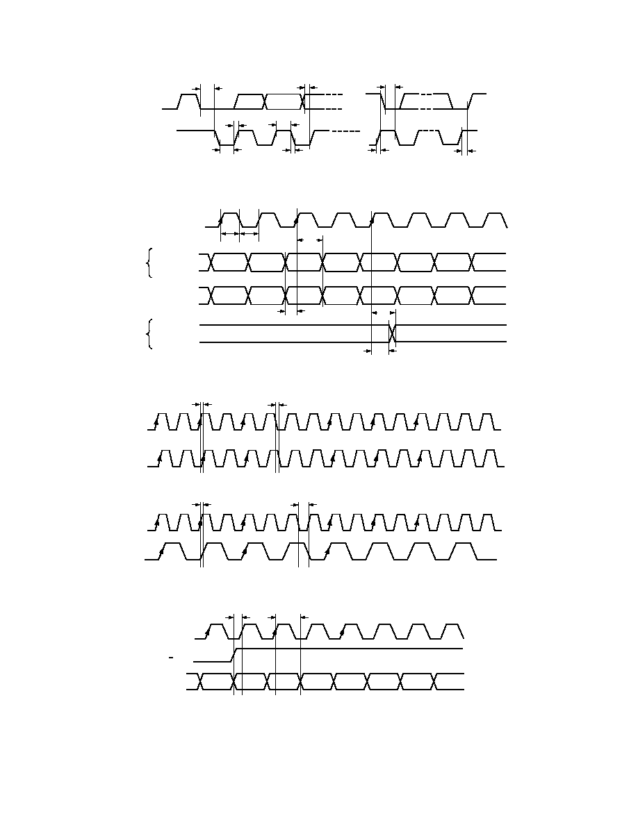
t
3
t
2
t
6
t
1
t
7
t
5
t
3
t
4
t
8
SDATA
SCLOCK
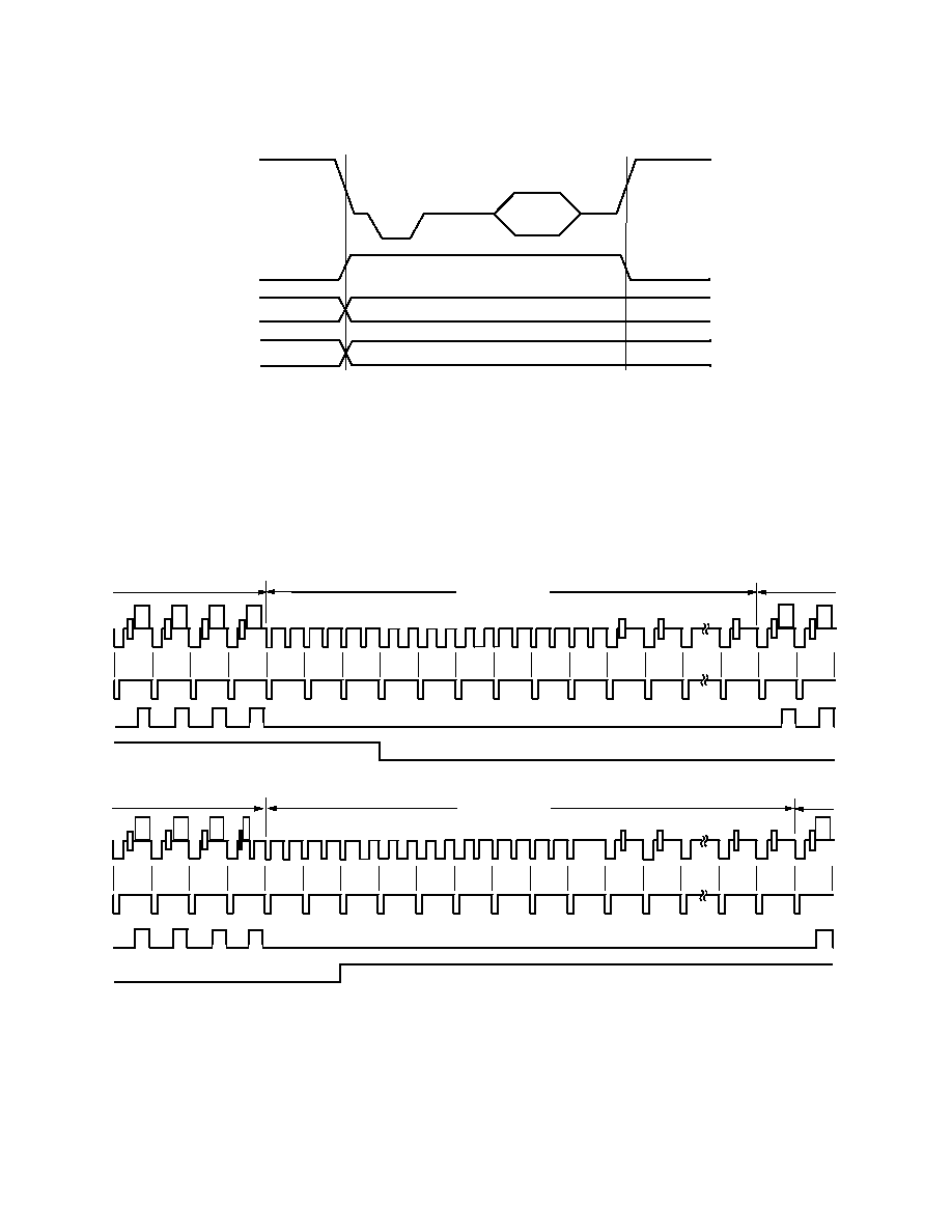
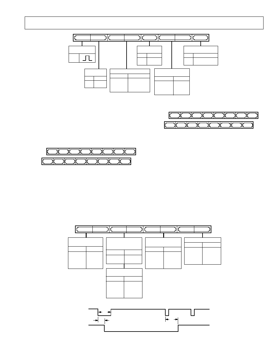
Figure 1. MPU Port Timing Diagram
t
9
t
11
CLOCK
PIXEL INPUT
DATA
t
10
t
12
HSYNC,
FIELD/
VSYNC,
BLANK
Cb
Y
Cr
Y
Cb
Y
HSYNC,
FIELD/
VSYNC,
BLANK
t
13
t
14
CONTROL
I/PS
CONTROL
O/PS
Figure 2. Pixel and Control Data Timing Diagram
t
16
t
17
t
17
t
16
CLOCK/2
CLOCK
CLOCK/2
CLOCK
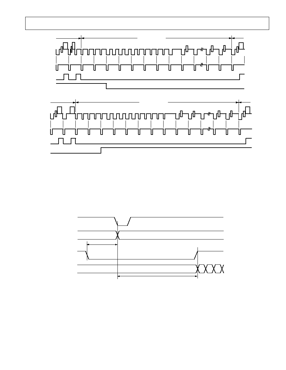
Figure 3. Internal Timing Diagram
t
18
CLOCK
OSD EN
t
19
OSD02
Figure 4. OSD Timing Diagram
ADV7177/ADV7178
9
REV. A
ABSOLUTE MAXIMUM RATINGS
1
V
AA
to GND . . . . . . . . . . . . . . . . . . . . . . . . . . . . . . . . . . . 7 V
Voltage on Any Digital Input Pin . . GND 0.5 V to V
AA
+ 0.5 V
Storage Temperature (T
S
) . . . . . . . . . . . . . . 65
°C to +150°C
Junction Temperature (T
J
) . . . . . . . . . . . . . . . . . . . . . . . 150
°C
Lead Temperature (Soldering, 10 sec) . . . . . . . . . . . . . . 260
°C
Analog Outputs to GND
2
. . . . . . . . . . . . . . GND 0.5 to V
AA
NOTES
1
Stresses above those listed under Absolute Maximum Ratings may cause permanent
damage to the device. This is a stress rating only; functional operation of the device
at these or any other conditions above those listed in the operational sections of this
specification is not implied. Exposure to absolute maximum rating conditions for
extended periods may affect device reliability.
2
Analog output short circuit to any power supply or common can be of an
indefinite duration.
ORDERING GUIDE
Temperature Package
Package
Model
Range
Description
Option
ADV7178KS
0
°C to 70°C
Plastic Quad Flatpack S-44
ADV7177KS
0
°C to 70°C
Plastic Quad Flatpack S-44
CAUTION
ESD (electrostatic discharge) sensitive device. Electrostatic charges as high as 4000 V readily
accumulate on the human body and test equipment and can discharge without detection.
Although the ADV7177/ADV7178 feature proprietary ESD protection circuitry, permanent
damage may occur on devices subjected to high-energy electrostatic discharges. Therefore,
proper ESD precautions are recommended to avoid performance degradation or loss of functionality.
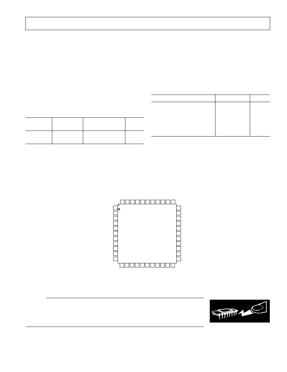
PIN CONFIGURATION
12 13 14 15 16 17 18 19 20 21 22
3
4
5
6
7
1
2
10
11
8
9
40 39 38
41
42
43
44
36 35 34
37
29
30
31
32
27
28
25
26
23
24
33
PIN 1
IDENTIFIER
R
SET
V
REF
DAC A
V
AA
GND
V
AA
DAC B
BLANK
P13
P14
P15
HSYNC
FIELD/
VSYNC
ALSB
V
AA
CLOCK/2
P5
P6
P7
P8
P9
P10
P11
P12
OSD_EN
DAC C
COMP
SDATA
SCLOCK
GND
V
AA
GND
RESET
CLOCK
CLOCK
GND
P4
P3
P2
P1
P0
OSD_2
OSD_1
OSD_0
ADV7177/ADV7178
PQFP
TOP VIEW
(Not to Scale)
PACKAGE THERMAL PERFORMANCE
The 44-lead PQFP package used for this device has a junction-
to-ambient thermal resistance (
JA
) in still air on a four-layer
PCB of 53.2
°C/W. The junction-to-case thermal resistance (
JC
)
is 18.8
°C/W.
Care must be taken when operating the part in certain condi-
tions to prevent overheating. Table I illustrates what conditions
are to be used when using the part.
Table I. Allowable Operating Conditions for ADV7177/
ADV7178 in 44-Lead PQFP Package
Condition
5 V
3 V
3 DACs ON, Double 75R
1
No
Yes
3 DACs ON, Low Power
2
Yes
Yes
3 DACs ON, Buffered
3
Yes
Yes
2 DACs ON, Double 75R
No
Yes
2 DACs ON, Low Power
Yes
Yes
2 DACs ON, Buffered
Yes
Yes
NOTES
1
DAC ON, Double 75R refers to a condition where the DACs are terminated
into a double 75R load and low power mode is disabled.
2
DAC ON, Low Power refers to a condition where the DACs are terminated in a
double 75R load and low power mode is enabled.
3
DAC ON, Buffered refers to a condition where the DAC current is reduced to
5 mA and external buffers are used to drive the video loads.
WARNING!
ESD SENSITIVE DEVICE

ADV7177/ADV7178
10
REV. A
PIN FUNCTION DESCRIPTIONS
Pin
Input/
No.
Mnemonic
Output
Function
1, 20, 28, 30
V
AA
P
Power Supply.
2
CLOCK/2
O
Synchronous Clock output signal. Can be either 27 MHz or 13.5 MHz; this
can be controlled by MR32 and MR33 in Mode Register 3.
310, 1214,
P15P0
I
8-Bit 4:2:2 Multiplexed YCrCb Pixel Port (P7P0) or 16-Bit YCrCb
3741
Pixel Port (P15P0). P0 represents the LSB.
11
OSD_EN
I
Enables OSD input data on the video outputs.
15
HSYNC
I/O
HSYNC (Modes 1 and 2) Control Signal. This pin may be configured to
output (Master Mode) or accept (Slave Mode) Sync signals.
16
FIELD/
VSYNC
I/O
Dual Function FIELD (Mode 1) and
VSYNC (Mode 2) Control Signal. This
pin may be configured to output (Master Mode) or accept (Slave Mode)
these control signals.
17
BLANK
I/O
Video Blanking Control Signal. The pixel inputs are ignored when this is
Logic Level "0." This signal is optional.
18
ALSB
I
TTL Address Input. This signal sets up the LSB of the MPU address.
19, 21, 29, 42
GND
G
Ground Pin.
22
RESET
I
The input resets the on-chip timing generator and sets the ADV7177/ADV7178
into default mode. This is NTSC operation, Timing Slave Mode 0, 8-Bit
Operation, 2
× Composite and S VHS out.
23
SCLOCK
I
MPU Port Serial Interface Clock Input.
24
SDATA
I/O
MPU Port Serial Data Input/Output.
25
COMP
O
Compensation Pin. Connect a 0.1
µF Capacitor from COMP to V
AA
.
26
DAC C
O
DAC C Analog Output.
27
DAC B
O
DAC B Analog Output.
31
DAC A
O
DAC A Analog Output.
32
V
REF
I/O
Voltage Reference Input for DACs or Voltage Reference Output (1.235 V).
33
R
SET
I
A 300
resistor connected from this pin to GND is used to control full-scale
amplitudes of the Video Signals.
3436
OSD_02
I
On Screen Display Inputs.
43
CLOCK
O
Crystal Oscillator output (to crystal). Leave unconnected if no crystal is used.
44
CLOCK
I
Crystal Oscillator input. If no crystal is used this pin can be driven by an
external TTL Clock source; it requires a stable 27 MHz reference Clock for
standard operation. Alternatively, a 24.5454 MHz (NTSC) or 29.5 MHz
(PAL)
can be used for square pixel operation.
ADV7177/ADV7178
11
REV. A
compatible with worldwide standards. The 4:2:2 YUV video
data is interpolated to two times the pixel rate. The color-
difference components (UV) are quadrature modulated using
a subcarrier frequency generated by an on-chip 32-bit digital
synthesizer (also running at two times the pixel rate). The two
times pixel rate sampling allows for better signal-to-noise ratio.
A 32-bit DDS with a 9-bit look-up table produces a superior
subcarrier in terms of both frequency and phase. In addition
to the composite output signal, there is the facility to output
S-Video (Y/C) video, YUV or RGB video.
Each analog output is capable of driving the full video-level
(34.7 mA) signal into an unbuffered, doubly terminated 75
load. With external buffering, the user has the additional option
to scale back the DAC output current to 5 mA min, thereby signifi-
cantly reducing the power dissipation of the device.
The ADV7177/ADV7178 also supports both PAL and NTSC
square pixel operation.
The output video frames are synchronized with the incoming
data timing reference codes. Optionally, the encoder accepts
(and can generate)
HSYNC, VSYNC and FIELD timing signals.
These timing signals can be adjusted to change pulsewidth and
position while the part is in the master mode. The encoder
requires a single two times pixel rate (27 MHz) clock for standard
operation. Alternatively, the encoder requires a 24.5454 MHz
clock for NTSC or 29.5 MHz clock for PAL square pixel mode
operation. All internal timing is generated on-chip.
The ADV7177/ADV7178 modes are set up over a two-wire
serial bidirectional port (I
2
C-Compatible) with two slave addresses.
Functionally the ADV7178 and ADV7177 are the same with
the exception that the ADV7178 can output the Macrovision
anticopy algorithm, and OSD is only supported on the ADV7177.
The ADV7177/ADV7178 is packaged in a 44-lead thermally
enhanced PQFP package.
DATA PATH DESCRIPTION
For PAL B, D, G, H, I, M, N and NTSC M, N modes, YCrCb
4:2:2 data is input via the CCIR-656 compatible pixel port at a
27 MHz data rate. The pixel data is demultiplexed to from three
data paths. Y typically has a range of 16 to 235, Cr and Cb
typically have a range of 128
± 112; however, it is possible to
input data from 1 to 254 on both Y, Cb and Cr. The
ADV7177/ADV7178 supports PAL (B, D, G, H, I, N, M) and
NTSC (with and without Pedestal) standards. The appropri-
ate SYNC,
BLANK and Burst levels are added to the YCrCb
data. Macrovision antitaping (ADV7178 only), closed captioning,
OSD (ADV7177 only), and teletext levels are also added to Y,
and the resultant data is interpolated to a rate of 27 MHz. The
interpolated data is filtered and scaled by three digital FIR filters.
The U and V signals are modulated by the appropriate subcarrier
sine/cosine phases and added together to make up the chromi-
nance signal. The luma (Y) signal can be delayed 13 luma
cycles (each cycle is 74 ns) with respect to the chroma signal.
The luma and chroma signals are then added together to make
up the composite video signal. All edges are slew rate limited.
The YCrCb data is also used to generate RGB data with
appropriate SYNC and
BLANK levels. The RGB data is in
synchronization with the composite video output. Alternatively
analog YUV data can be generated instead of RGB.
The three 9-bit DACs can be used to output:
1. RGB Video.
2. YUV Video
3. One Composite Video Signal + LUMA and CHROMA
3.
(S-Video).
Alternatively, each DAC can be individually powered off if
not required.
Video output levels are illustrated in Appendix 3.
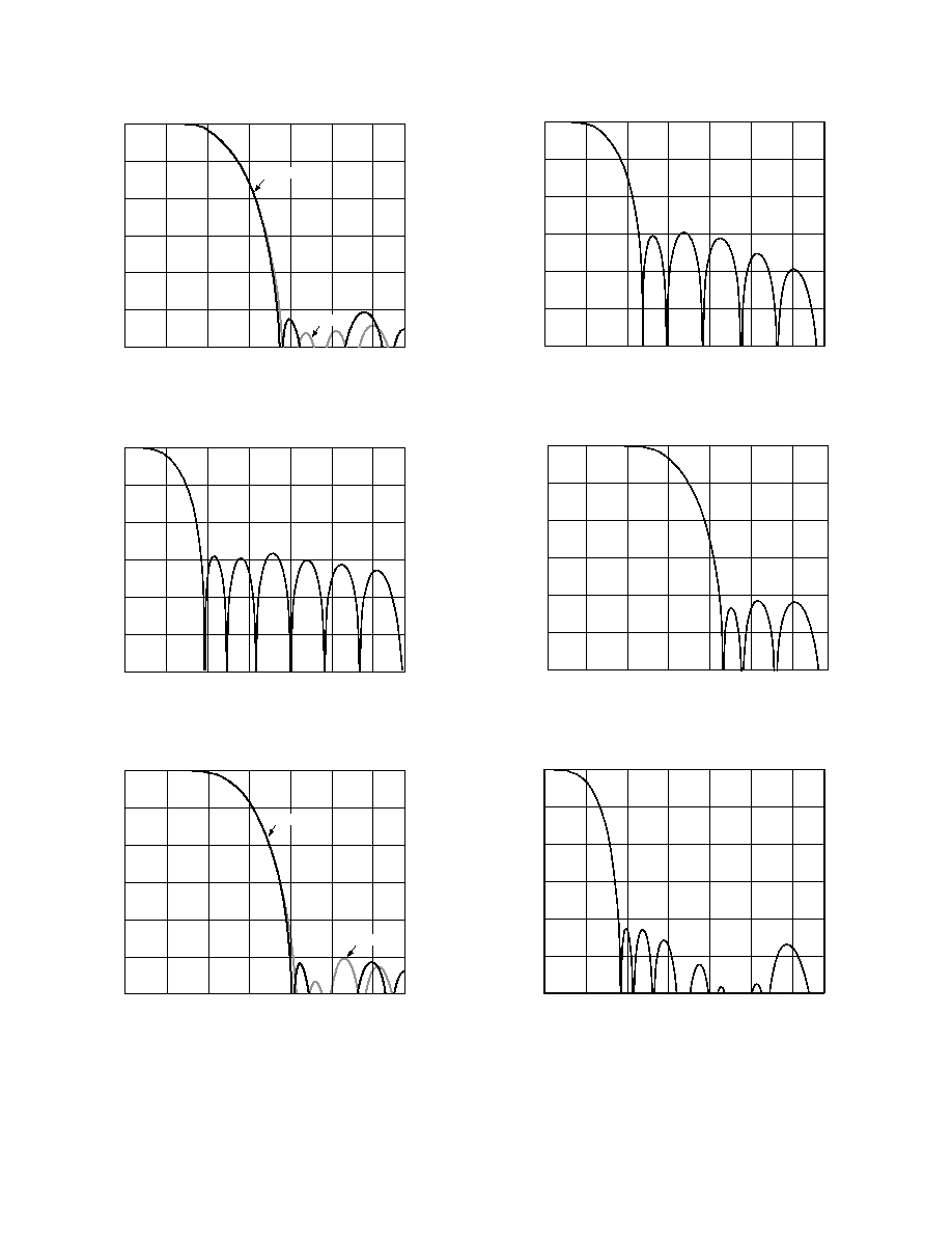
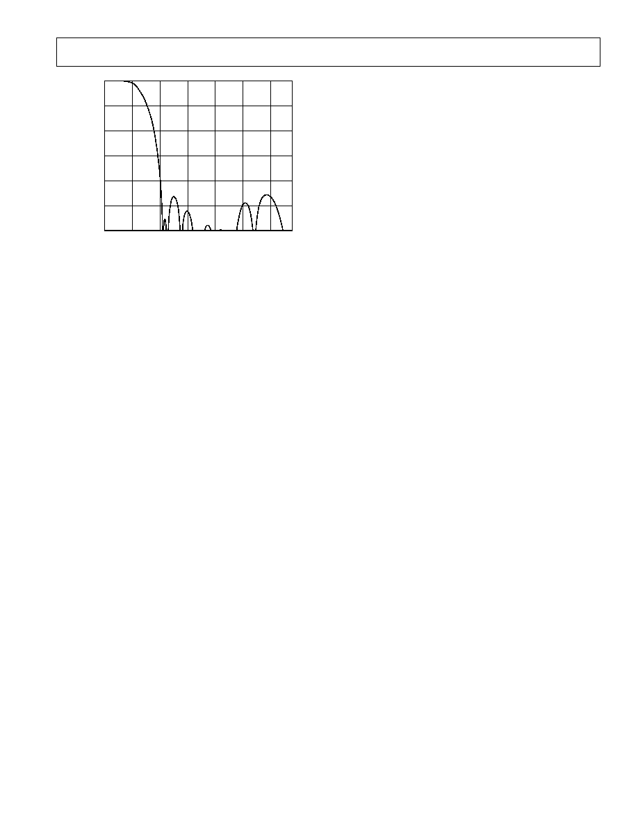
INTERNAL FILTER RESPONSE
The Y filter supports several different frequency responses,
including two 4.5 MHz/5.0 MHz low-pass responses, PAL/
NTSC subcarrier notch responses and a PAL/NTSC extended
response. The U and V filters have a 1.0/1.3 MHz low-pass
response for NTSC/PAL. These filter characteristics are illus-
trated in Figures 7 to 13.
(Continued from page 1)
MR04
MR03
NTSC
0
0
2.3
0.026
7.0
>
54
4.2
PAL
0
0
3.4
0.098
7.3
>
50
5.0
NTSC
0
1
1.0
0.085
3.57
>
27.6
2.1
PAL
0
1
1.4
0.107
4.43
>
29.3
2.7
NTSC/PAL
1 0
4.0
0.150
7.5
>
40
5.35
NTSC
1
1
2.3
0.054
7.0
>
54
4.2
PAL
1
1
3.4
0.106
7.3
>
50.3
5.0
FILTER SELECTION
F
3 dB
PASSBAND
CUTOFF (MHz)
STOPBAND
CUTOFF (MHz)
PASSBAND
RIPPLE (dB)
STOPBAND
ATTENUATION (dB)
Figure 5. Luminance Internal Filter Specifications
NTSC
1.0
0.085
3.2
>
40
0.3
2.05
PAL
1.3
0.04
4.0
>
40
0.02
2.45
FILTER SELECTION
F
3 dB
PASSBAND
CUTOFF (MHz)
STOPBAND
CUTOFF (MHz)
PASSBAND
RIPPLE (dB)
STOPBAND
ATTENUATION (dB)
ATTENUATION @
1.3MHz (dB)
Figure 6. Chrominance Internal Filter Specifications
ADV7177/ADV7178
12
REV. A
FREQUENCY MHz
0
60
50
40
10
20
30
0
2
4
6
AMPLITUDE
dB
8
12
10
TYPE A
TYPE B
Figure 7. NTSC Low-Pass Filter
FREQUENCY MHz
0
60
50
40
10
20
30
0
2
4
6
8
12
10
AMPLITUDE
dB
Figure 8. NTSC Notch Filter
FREQUENCY MHz
0
60
50
40
10
20
30
0
2
4
6
8
12
10
AMPLITUDE
dB
TYPE B
TYPE A
Figure 9. PAL Low-Pass Filter
FREQUENCY MHz
0
60
50
40
10
20
30
0
2
4
6
8
12
10
AMPLITUDE
dB
Figure 10. PAL Notch Filter
FREQUENCY MHz
60
50
40
10
20
30
0
2
4
6
8
12
10
AMPLITUDE
dB
0
Figure 11. NTSC/PAL Extended Mode Filter
FREQUENCY MHz
0
60
50
40
10
20
30
0
2
4
6
8
12
10
AMPLITUDE
dB
Figure 12. NTSC UV Filter
ADV7177/ADV7178
13
REV. A
FREQUENCY MHz
0
60
50
40
10
20
30
0
2
4
6
8
12
10
AMPLITUDE
dB
Figure 13. PAL UV Filter
COLOR BAR GENERATION
The ADV7177/ADV7178 can be configured to generate 100/
7.5/75/7.5 color bars for NTSC or 100/0/75/0 for PAL color
bars. These are enabled by setting MR17 of Mode Register 1 to
Logic "1."
SQUARE PIXEL MODE
The ADV7177/ADV7178 can be used to operate in square pixel
mode. For NTSC operation an input clock of 24.5454 MHz is
required. Alternatively an input clock of 29.5 MHz is required
for PAL operation. The internal timing logic adjusts accordingly
for square pixel mode operation.
COLOR SIGNAL CONTROL
The color information can be switched on and off the video
output using Bit MR24 of Mode Register 2.
BURST SIGNAL CONTROL
The burst information can be switched on and off the video
output using Bit MR25 of Mode Register 2.
NTSC PEDESTAL CONTROL
The pedestal on both odd and even fields can be controlled on a
line-by-line basis using the NTSC Pedestal Control Registers.
This allows the pedestals to be controlled during the vertical
blanking interval.
PIXEL TIMING DESCRIPTION
The ADV7177/ADV7178 can operate in either 8-bit or 16-bit
YCrCb Mode.
8-Bit YCrCb Mode
This default mode accepts multiplexed YCrCb inputs through
the P7P0 pixel inputs. The inputs follow the sequence Cb0, Y0
Cr0, Y1 Cb1, Y2, etc. The Y, Cb and Cr data are input on a
rising clock edge.
16-Bit YCrCb Mode
This mode accepts Y inputs through the P7P0 pixel inputs and
multiplexed CrCb inputs through the P15P8 pixel inputs. The
data is loaded on every second rising edge of CLOCK. The inputs
follow the sequence Cb0, Y0 Cr0, Y1 Cb1, Y2, etc.
OSD
The ADV7177 supports OSD. There are twelve 8-bit OSD
registers, loaded with data from the four most significant bits of
Y, Cb, Cr input pixel data bytes. A choice of eight colors can,
therefore, be selected via the OSD_0, OSD_1, OSD_2 pins,
each color being a combination of 12 bits of Y, Cb, Cr pixel
data. The display is under control of the OSD_EN pin. The
OSD window can be an entire screen or just one pixel, its size
may change by using the OSD_EN signal to control the width on a
line-by-line basis. Figure 4 illustrates OSD timing on the ADV7177.
VIDEO TIMING DESCRIPTION
The ADV7177/ADV7178 is intended to interface to off-the-shelf
MPEG1 and MPEG2 decoders. Consequently, the ADV7177/
ADV7178 accepts 4:2:2 YCrCb pixel data via a CCIR-656 pixel
port, and has several video timing modes of operation that allow
it to be configured as either system master video timing genera-
tor or a slave to the system video timing generator. The ADV7177/
ADV7178 generates all of the required horizontal and vertical
timing periods and levels for the analog video outputs.
The ADV7177/ADV7178 calculates the width and placement of
analog sync pulses, blanking levels and color burst envelopes.
Color bursts are disabled on appropriate lines, and serration and
equalization pulses are inserted where required.
In addition, the ADV7177/ADV7178 supports a PAL or NTSC
square pixel operation in slave mode. The part requires an input
pixel clock of 24.5454 MHz for NTSC and an input pixel clock
of 29.5 MHz for PAL. The internal horizontal line counters
place the various video waveform sections in the correct location
for the new clock frequencies.
The ADV7177/ADV7178 has four distinct master and four
distinct slave timing configurations. Timing Control is estab-
lished with the bidirectional
SYNC, BLANK and FIELD/
VSYNC pins. Timing Mode Register 1 can also be used to vary
the timing pulsewidths and where they occur in relation to
each other.
ADV7177/ADV7178
14
REV. A
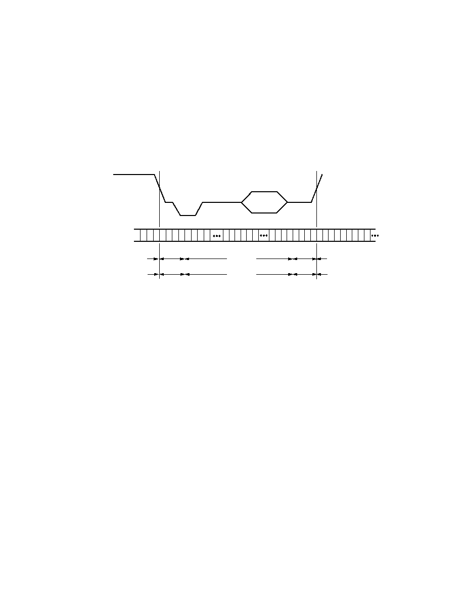
Vertical Blanking Data Insertion
It is possible to allow encoding of incoming YCbCr data on those lines of VBI that do not bear line sync or pre-/post-equalization
pulses (see Figures 14 to 25). This mode of operation is called "Partial Blanking" and is selected by setting MR31 to 1. It allows the
insertion of any VBI data (Opened VBI) into the encoded output waveform. This data is present in digitized incoming YCbCr data
stream (e.g., WSS data, CGMS, VPS, etc.). Alternatively, the entire VBI may be blanked (no VBI data inserted) on these lines by
setting MR31 to 0.
Mode 0 (CCIR-656): Slave Option
(Timing Register 0 TR0 = X X X X X 0 0 0)
The ADV7177/ADV7178 is controlled by the SAV (Start Active Video) and EAV (End Active Video) time codes in the pixel data.
All timing information is transmitted using a 4-byte synchronization pattern. A synchronization pattern is sent immediately before
and after each line during active picture and retrace. Mode 0 is illustrated in Figure 14. The
HSYNC, FIELD/VSYNC and BLANK
(if not used) pins should be tied high during this mode.
Y
C
r
Y
F
F
0
0
0
0
X
Y
8
0
1
0
8
0
1
0
F
F
0
0
F
F
A
B
A
B
A
B
8
0
1
0
8
0
1
0
F
F
0
0
0
0
X
Y
C
b
Y C
r
C
b
Y
C
b
Y
C
r
EAV CODE
SAV CODE
ANCILLARY DATA
(HANC)
4 CLOCK
4 CLOCK
268 CLOCK
1440 CLOCK
4 CLOCK
4 CLOCK
280 CLOCK
1440 CLOCK
END OF ACTIVE
VIDEO LINE
START OF ACTIVE
VIDEO LINE
ANALOG
VIDEO
INPUT PIXELS
NTSC/PAL M SYSTEM
(525 LlNES/60Hz)
PAL SYSTEM
(625 LINES/50Hz)
Y
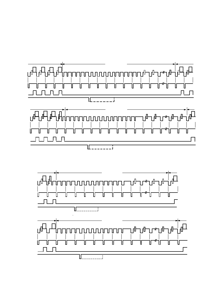
Figure 14. Timing Mode 0 (Slave Mode)
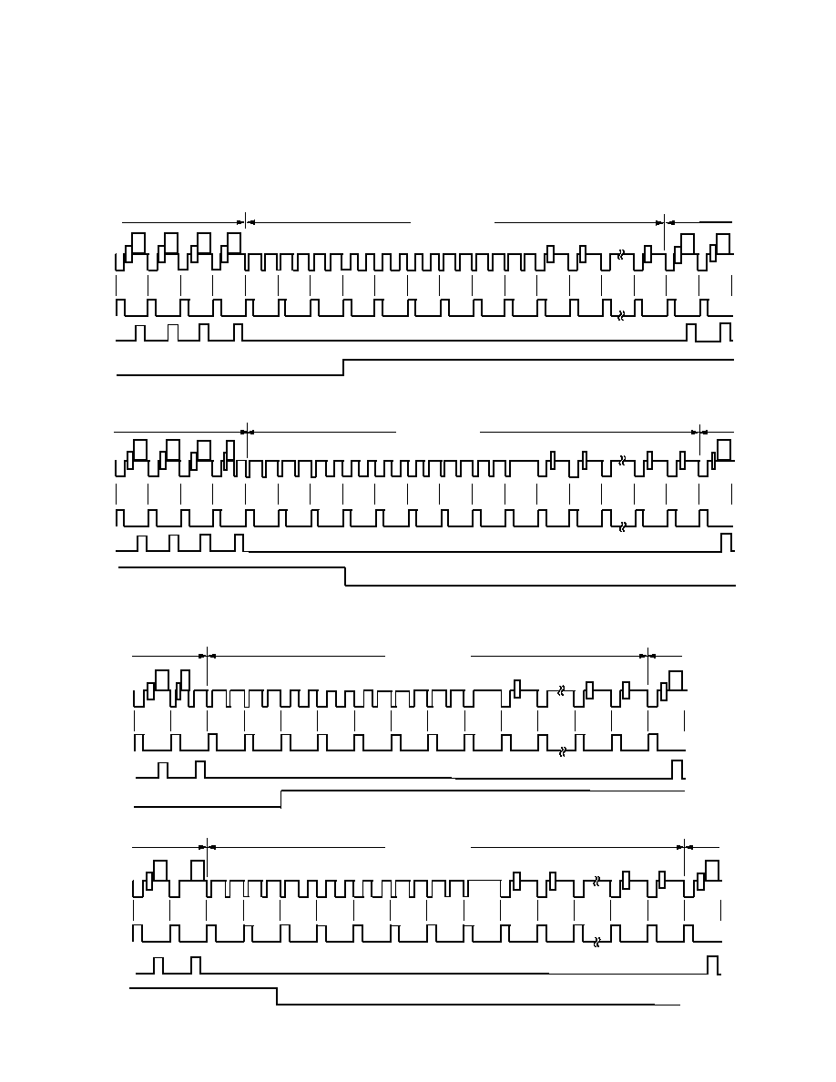
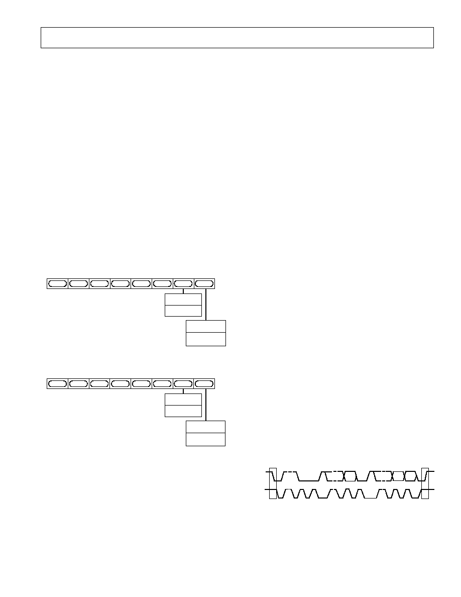
Mode 0 (CCIR-656): Master Option
(Timing Register 0 TR0 = X X X X X 0 0 1)
The ADV7177/ADV7178 generates H, V and F signals required for the SAV (Start Active Video) and EAV (End Active Video) time
codes in the CCIR-656 standard. The H bit is output on the
HSYNC pin, the V bit is output on the BLANK pin, and the F bit is
output on the FIELD/
VSYNC pin. Mode 0 is illustrated in Figure 15 (NTSC) and Figure 16 (PAL). The H, V and F transitions
relative to the video waveform are illustrated in Figure 17.
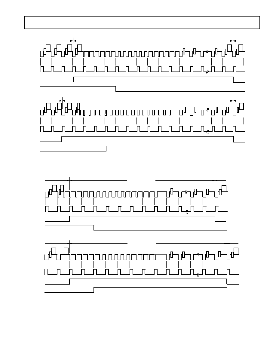
ADV7177/ADV7178
15
REV. A
522
523
524
525
1
2
3
4
5
6
7
8
9
10
11
20
21
22
DISPLAY
DISPLAY
VERTICAL BLANK
ODD FIELD
EVEN FIELD
H
V
F
260
261
262
263
264
265
266
267
268
269
270
271
272
273
274
283
284
285
ODD FIELD
EVEN FIELD
DISPLAY
DISPLAY
VERTICAL BLANK
H
V
F
Figure 15. Timing Mode 0 (NTSC Master Mode)
622
623
624
625
1
2
3
4
5
6
7
21
22
23
DISPLAY
DISPLAY
VERTICAL BLANK
H
V
F
ODD FIELD
EVEN FIELD
309
310
311
312
314
315
316
317
318
319
320
334
335
336
DISPLAY
DISPLAY
VERTICAL BLANK
H
V
F
ODD FIELD
EVEN FIELD
313
Figure 16. Timing Mode 0 (PAL Master Mode)
ADV7177/ADV7178
16
REV. A
ANALOG
VIDEO
H
F
V
Figure 17. Timing Mode 0 Data Transitions (Master Mode)
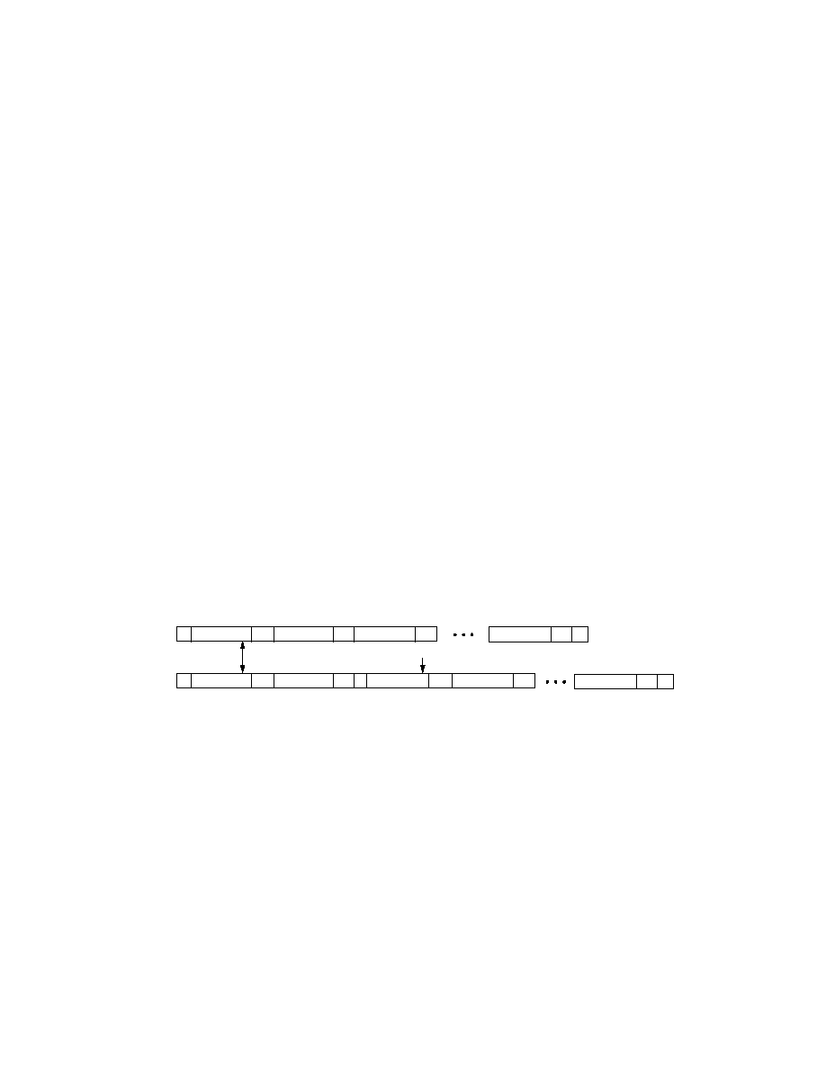
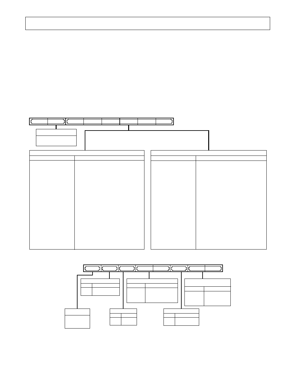
Mode 1: Slave Option
HSYNC, BLANK, FIELD
(Timing Register 0 TR0 = X X X X X 0 1 0)
In this mode the ADV7177/ADV7178 accepts horizontal SYNC and Odd/Even FIELD signals. A transition of the FIELD input
when
HSYNC is low indicates a new frame, i.e., vertical retrace. The BLANK signal is optional. When the BLANK input is
disabled, the ADV7177/ADV7178 automatically blanks all normally blank lines. Mode 1 is illustrated in Figure 18 (NTSC) and
Figure 19 (PAL).
260
261
262
263
264
265
266
267
268
269
270
271
272
273
274
283
284
285
ODD FIELD
EVEN FIELD
DISPLAY
DISPLAY
HSYNC
BLANK
FIELD
522
523
524
525
1
2
3
4
5
6
7
8
9
10
11
20
21
22
DISPLAY
DISPLAY
ODD FIELD
EVEN FIELD
HSYNC
BLANK
FIELD
VERTICAL BLANK
VERTICAL BLANK
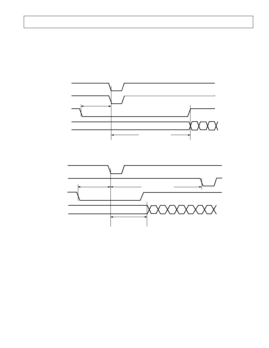
Figure 18. Timing Mode 1 (NTSC)
ADV7177/ADV7178
17
REV. A
622
623
624
625
1
2
3
4
5
6
7
21
22
23
DISPLAY
ODD FIELD
EVEN FIELD
HSYNC
BLANK
FIELD
DISPLAY
309
310
311
312
313
314
315
316
317
318
319
334
335
336
DISPLAY
ODD FIELD
EVEN FIELD
HSYNC
BLANK
FIELD
DISPLAY
320
VERTICAL BLANK
VERTICAL BLANK
Figure 19. Timing Mode 1 (PAL)
Mode 1: Master Option
HSYNC, BLANK, FIELD
(Timing Register 0 TR0 = X X X X X 0 1 1)
In this mode the ADV7177/ADV7178 can generate horizontal SYNC and Odd/Even FIELD signals. A transition of the FIELD
input when
HSYNC is low indicates a new frame, i.e., vertical retrace. The BLANK signal is optional. When the BLANK input is
disabled, the ADV7177/ADV7178 automatically blanks all normally blank lines. Pixel data is latched on the rising clock edge follow-
ing the timing signal transitions. Mode 1 is illustrated in Figure 18 (NTSC) and Figure 19 (PAL). Figure 20 illustrates the
HSYNC,
BLANK and FIELD for an odd or even field transition relative to the pixel data.
FIELD
PIXEL
DATA
PAL = 12
*
CLOCK/2
NTSC = 16
*
CLOCK/2
PAL = 132
*
CLOCK/2
NTSC = 122
*
CLOCK/2
Cb
Y
Cr
Y
HSYNC
BLANK
Figure 20. Timing Mode 1 Odd/Even Field Transitions Master/Slave
ADV7177/ADV7178
18
REV. A
Mode 2: Slave Option
HSYNC, VSYNC, BLANK
(Timing Register 0 TR0 = X X X X X 1 0 0)
In this mode the ADV7177/ADV7178 accepts horizontal and vertical SYNC signals. A coincident low transition of both
HSYNC and
VSYNC inputs indicates the start of an odd field. A VSYNC low transition when HSYNC is high indicates the start of an even field.
The
BLANK signal is optional. When the BLANK input is disabled, the ADV7177/ADV7178 automatically blanks all normally
blank lines as per CCIR-624. Mode 2 is illustrated in Figure 21 (NTSC) and Figure 22 (PAL).
522
523
524
525
1
2
3
4
5
6
7
8
9
10
11
20
21
22
DISPLAY
DISPLAY
ODD FIELD
EVEN FIELD
HSYNC
BLANK
VSYNC
260
261
262
263
264
265
266
267
268
269
270
271
272
273
274
283
284
285
ODD FIELD
EVEN FIELD
DISPLAY
DISPLAY
HSYNC
BLANK
VSYNC
VERTICAL BLANK
VERTICAL BLANK
Figure 21. Timing Mode 2 (NTSC)
622
623
624
625
1
2
3
4
5
6
7
21
22
23
DISPLAY
ODD FIELD
EVEN FIELD
HSYNC
BLANK
VSYNC
DISPLAY
309
310
311
312
313
314
315
316
317
318
319
334
335
336
DISPLAY
ODD FIELD
EVEN FIELD
HSYNC
BLANK
DISPLAY
320
VSYNC
VERTICAL BLANK
VERTICAL BLANK
Figure 22. Timing Mode 2 (PAL)
ADV7177/ADV7178
19
REV. A
Mode 2: Master Option
HSYNC, VSYNC, BLANK
(Timing Register 0 TR0 = X X X X X 1 0 1)
In this mode, the ADV7177/ADV7178 can generate horizontal and vertical SYNC signals. A coincident low transition of both
HSYNC and VSYNC inputs indicates the start of an Odd Field. A VSYNC low transition when HSYNC is high indicates the start
of an even field. The
BLANK signal is optional. When the BLANK input is disabled, the ADV7177/ADV7178 automatically blanks
all normally blank lines as per CCIR-624. Mode 2 is illustrated in Figure 21 (NTSC) and Figure 22 (PAL). Figure 23 illustrates the
HSYNC, BLANK and VSYNC for an even-to-odd field transition relative to the pixel data. Figure 24 illustrates the HSYNC,
BLANK and VSYNC for an odd-to-even field transition relative to the pixel data.
PAL = 12
*
CLOCK/2
NTSC = 16
*
CLOCK/2
HSYNC
VSYNC
BLANK
PIXEL
DATA
PAL = 132
*
CLOCK/2
NTSC = 122
*
CLOCK/2
Cb
Y
Cr
Figure 23. Timing Mode 2 Even-to-Odd Field Transition Master/Slave
PAL = 864
*
CLOCK/2
NTSC = 858
*
CLOCK/2
PAL = 132
*
CLOCK/2
NTSC = 122
*
CLOCK/2
HSYNC
VSYNC
BLANK
PIXEL
DATA
PAL = 12
*
CLOCK/2
NTSC = 16
*
CLOCK/2
Cb
Y
Cr
Y
Cb
Figure 24. Timing Mode 2 Odd-to-Even Field Transition Master/Slave
ADV7177/ADV7178
20
REV. A
Mode 3: Master/Slave Option
HSYNC, BLANK, FIELD
(Timing Register 0 TR0 = X X X X X 1 1 0 or X X X X X 1 1 1)
In this mode, the ADV7177/ADV7178 accepts or generates Horizontal SYNC and Odd/Even FIELD signals. A transition of the
FIELD input when
HSYNC is high indicates a new frame, i.e., vertical retrace. The BLANK signal is optional. When the BLANK
input is disabled, the ADV7177/ADV7178 automatically blanks all normally blank lines as per CCIR-624. Mode 3 is illustrated in
Figure 25 (NTSC) and Figure 26 (PAL).
522
523
524
525
1
2
3
4
5
6
7
8
9
10
11
20
21
22
DISPLAY
DISPLAY
VERTICAL BLANK
ODD FIELD
EVEN FIELD
BLANK
FIELD
260
261
262
263
264
265
266
267
268
269
270
271
272
273
274
283
284
285
EVEN FIELD
DISPLAY
DISPLAY
VERTICAL BLANK
HSYNC
ODD FIELD
BLANK
FIELD
HSYNC
Figure 25. Timing Mode 3 (NTSC)
622
623
624
625
1
2
3
4
5
6
7
21
22
23
DISPLAY
DISPLAY
VERTICAL BLANK
ODD FIELD
EVEN FIELD
BLANK
FIELD
309
310
311
312
314
315
316
317
318
319
320
334
335
336
DISPLAY
DISPLAY
VERTICAL BLANK
ODD FIELD
EVEN FIELD
313
HSYNC
BLANK
FIELD
HSYNC
Figure 26. Timing Mode 3 (PAL)
ADV7177/ADV7178
21
REV. A
POWER-ON RESET
After power-up, it is necessary to execute a reset operation. A
reset occurs on the falling edge of a high-to-low transition on
the
RESET pin. This initializes the pixel port so that the
pixel inputs, P7P0 are selected. After reset, the ADV7177/
ADV7178 is automatically set up to operate in NTSC mode.
Subcarrier frequency code 21F07C16HEX is loaded into the
subcarrier frequency registers. All other registers, with the
exception of Mode Register 0, are set to 00H. All bits in Mode
Register 0 are set to Logic Level "0" except Bit MR02. Bit
MR02 of Mode Register 0 is set to Logic Level "1." This enables
the 7.5 IRE pedestal.
MPU PORT DESCRIPTION
The ADV7178 and ADV7177 support a two-wire serial (I
2
C-
Compatible) microprocessor bus driving multiple peripherals.
Two inputs, serial data (SDATA) and serial clock (SCLOCK),
carry information between any device connected to the bus. Each
slave device is recognized by a unique address. The ADV7178 and
ADV7177 each have four possible slave addresses for both read
and write operations. These are unique addresses for each device
and are illustrated in Figure 27 and Figure 28. The LSB sets
either a read or write operation. Logic Level "1" corresponds to
a read operation, while Logic Level "0" corresponds to a write
operation. A1 is set by setting the ALSB pin of the ADV7177/
ADV7178 to Logic Level "0" or Logic Level "1."
1
X
1
0
1
0
1
A1
ADDRESS
CONTROL
SET UP BY
ALSB
READ/WRITE
CONTROL
0
WRITE
1
READ
Figure 27. ADV7177 Slave Address
0
X
1
0
1
0
1
A1
ADDRESS
CONTROL
SET UP BY
ALSB
READ/WRITE
CONTROL
0
WRITE
1
READ
Figure 28. ADV7178 Slave Address
To control the various devices on the bus, the following proto-
col must be followed: First, the master initiates a data transfer by
establishing a start condition, defined by a high-to-low transition
on SDATA while SCLOCK remains high. This indicates that
an address/data stream will follow. All peripherals respond to
the start condition and shift the next eight bits (7-bit address
+ R/
W bit). The bits transfer from MSB down to LSB. The
peripheral that recognizes the transmitted address responds by
pulling the data line low during the ninth clock pulse. This is
known as an acknowledge bit. All other devices withdraw from
the bus at this point and maintain an idle condition. The idle
condition is where the device monitors the SDATA and SCLOCK
lines waiting for the start condition and the correct transmitted
address. The R/
W bit determines the direction of the data. A
Logic "0" on the LSB of the first byte means that the master
will write information to the peripheral. A Logic "1" on the
LSB of the first byte means that the master will read informa-
tion from the peripheral.
The ADV7177/ADV7178 acts as a standard slave device on the
bus. The data on the SDATA pin is 8 bits long, supporting
the 7-bit addresses, plus the R/
W bit. The ADV7178 has 36
subaddresses and the ADV7177 has 31 subaddresses to enable
access to the internal registers. It therefore interprets the first
byte as the device address and the second byte as the starting
subaddress. The subaddresses auto increment allows data to
be written to or read from the starting subaddress. A data
transfer is always terminated by a stop condition. The user can
also access any unique subaddress register on a one-by-one basis
without having to update all the registers. There is one excep-
tion. The subcarrier frequency registers should be updated in
sequence, starting with Subcarrier Frequency Register 0. The
auto increment function should then be used to increment and
access Subcarrier Frequency Registers 1, 2 and 3. The subcarrier
frequency registers should not be accessed independently.
Stop and start conditions can be detected at any stage during
the data transfer. If these conditions are asserted out of sequence
with normal read and write operations, they cause an immediate
jump to the idle condition. During a given SCLOCK high
period, the user should issue only one start condition, one stop
condition or a single stop condition followed by a single start
condition. If an invalid subaddress is issued by the user, the
ADV7177/ADV7178 will not issue an acknowledge and will
return to the idle condition. If, in auto-increment mode, the
user exceeds the highest subaddress, the following action will
be taken:
1. In Read Mode, the highest subaddress register contents
will continue to be output until the master device issues
a no-acknowledge. This indicates the end of a read. A no-
acknowledge condition is where the SDATA line is not
pulled low on the ninth pulse.
2. In Write Mode, the data for the invalid byte will not be
loaded into any subaddress register, a no-acknowledge will
be issued by the ADV7177/ADV7178 and the part will return
to the idle condition.
Figure 29 illustrates an example of data transfer for a read
sequence and the start and stop conditions.
1-7
8
9
1-7
8
9
1-7
8
9
P
S
START ADDR R/
W ACK SUBADDRESS ACK
DATA
ACK
STOP
SDATA
SCLOCK
Figure 29. Bus Data Transfer
ADV7177/ADV7178
22
REV. A
Figure 30 shows bus write and read sequences.
REGISTER ACCESSES
The MPU can write to or read from all of the ADV7177/
ADV7178 registers except the subaddress register, which is a
write-only register. The subaddress register determines which
register the next read or write operation accesses. All communi-
cations with the part through the bus start with an access to the
subaddress register. A read/write operation is performed from/to
the target address, which then increments to the next address
until a stop command on the bus is performed.
REGISTER PROGRAMMING
The following section describes each register, including subaddress
register, mode registers, subcarrier frequency registers, subcarrier
phase register, timing registers, closed captioning extended data
registers, closed captioning data registers and NTSC pedestal
control registers in terms of its configuration.
Subaddress Register (SR7SR0)
The communications register is an 8-bit write-only register.
After the part has been accessed over the bus, and a read/write
operation is selected, the subaddress is set up. The subaddress
register determines to/from which register the operation takes
place.
Figure 31 shows the various operations under the control of
the subaddress register. Zero should always be written to
SR7SR6.
Register Select (SR5SR0)
These bits are set up to point to the required starting address.
MODE REGISTER 0 MR0 (MR07MR00)
(Address [SR4SR0] = 00H)
Figure 32 shows the various operations under the control of Mode
Register 0. This register can be read from as well as written to.
MR0 BIT DESCRIPTION
Output Video Standard Selection (MR01MR00)
These bits are used to set up the encode mode. The ADV7177/
ADV7178 can be set up to output NTSC, PAL (B, D, G, H, I)
and PAL (M) standard video.
Pedestal Control (MR02)
This bit specifies whether a pedestal is to be generated on
the NTSC composite video signal. This bit is invalid if the
ADV7177/ADV7178 is configured in PAL mode.
Luminance Filter Control (MR04MR03)
The luminance filters are divided into two sets (NTSC/PAL) of
four filters, low-pass A, low-pass B, notch and extended. When
PAL is selected, bits MR03 and MR04 select one of four PAL
luminance filters; likewise, when NTSC is selected, bits MR03
and MR04 select one of four NTSC luminance filters. The
filters are illustrated in Figures 7 to 13.
RGB Sync (MR05)
This bit is used to set up the RGB outputs with the sync infor-
mation encoded on all RGB outputs.
Output Select (MR06)
This bit specifies if the part is in composite video or RGB/YUV
mode. Please note that the main composite signal is still avail-
able in RGB/YUV mode.
DATA
A(S)
S
SLAVE ADDR A(S)
SUB ADDR
A(S)
LSB = 0
LSB = 1
DATA
A(S) P
S
SLAVE ADDR A(S)
SUB ADDR
A(S) S
SLAVE ADDR
A(S)
DATA
A(M)
A(M)
DATA
P
WRITE
SEQUENCE
READ
SEQUENCE
A(S) = NO-ACKNOWLEDGE BY SLAVE
A(M) = NO-ACKNOWLEDGE BY MASTER
A(S) = ACKNOWLEDGE BY SLAVE
A(M) = ACKNOWLEDGE BY MASTER
S = START BIT
P = STOP BIT
Figure 30. Write and Read Sequences
ADV7177/ADV7178
23
REV. A
MODE REGISTER 1 MR1 (MR17MR10)
(Address (SR4SR0) = 01H)
Figure 33 shows the various operations under the control of Mode
Register 1. This register can be read from as well as written to.
MR1 BIT DESCRIPTION
Interlaced Mode Control (MR10)
This bit is used to set up the output to interlaced or noninter-
laced mode. This mode is only relevant when the part is in
composite video mode.
Closed Captioning Field Selection (MR12MR11)
These bits control the fields on which closed captioning data is
displayed; closed captioning information can be displayed on an
odd field, even field or both fields.
DAC Control (MR15MR13)
These bits can be used to power down the DACs. This can
be used to reduce the power consumption of the ADV7177/
ADV7178 if any of the DACs are not required in the application.
Color Bar Control (MR17)
This bit can be used to generate and output an internal color
bar test pattern. The color bar configuration is 100/7.5/75/7.5
for NTSC and 100/0/75/0 for PAL. It is important to note that
when color bars are enabled the ADV7177/ADV7178 is config-
ured in a master timing mode as per the one selected by bits
TR01 and TR02.
SR4
SR3
SR2
SR1
SR0
SR7
SR6
SR5
SR5
SR4 SR3 SR2 SR1 SR0
ADV7178 SUBADDRESS REGISTER
0
0
0
0
0
0
MODE REGISTER 0
0
0
0
0
0
1
MODE REGISTER 1
0
0
0
0
1
0
SUBCARRIER FREQ REGISTER 0
0
0
0
0
1
1
SUBCARRIER FREQ REGISTER 1
0
0
0
1
0
0
SUBCARRIER FREQ REGISTER 2
0
0
0
1
0
1
SUBCARRIER FREQ REGISTER 3
0
0
0
1
1
0
SUBCARRIER PHASE REGISTER
0
0
0
1
1
1
TIMING REGISTER 0
0
0
1
0
0
0
CLOSED CAPTIONING EXTENDED DATA BYTE 0
0
0
1
0
0
1
CLOSED CAPTIONING EXTENDED DATA BYTE 1
0
0
1
0
1
0
CLOSED CAPTIONING DATA BYTE 0
0
0
1
0
1
1
CLOSED CAPTIONING DATA BYTE 1
0
0
1
1
0
0
TIMING REGISTER 1
0
0
1
1
0
1
MODE REGISTER 2
0
0
1
1
1
0
NTSC PEDESTAL CONTROL REG 0 (FIELD 1/3)
0
0
1
1
1
1
NTSC PEDESTAL CONTROL REG 1 (FIELD 1/3)
0
1
0
0
0
0
NTSC PEDESTAL CONTROL REG 2 (FIELD 2/4)
0
1
0
0
0
1
NTSC PEDESTAL CONTROL REG 3 (FIELD 2/4)
0
1
0
0
1
0
MODE REGISTER 3
0
1
0
0
1
1
MACROVISION REGISTER
·
·
·
·
·
· " "
·
·
·
·
·
· " "
1
0
0
0
1
1
MACROVISION REGISTER
ZERO SHOULD BE WRITTEN
TO THESE BITS
SR7SR6 (00)
SR5
SR4 SR3 SR2 SR1 SR0
ADV7177 SUBADDRESS REGISTER
0
0
0
0
0
0
MODE REGISTER 0
0
0
0
0
0
1
MODE REGISTER 1
0
0
0
0
1
0
SUBCARRIER FREQ REGISTER 0
0
0
0
0
1
1
SUBCARRIER FREQ REGISTER 1
0
0
0
1
0
0
SUBCARRIER FREQ REGISTER 2
0
0
0
1
0
1
SUBCARRIER FREQ REGISTER 3
0
0
0
1
1
0
SUBCARRIER PHASE REGISTER
0
0
0
1
1
1
TIMING REGISTER 0
0
0
1
0
0
0
CLOSED CAPTIONING EXTENDED DATA
BYTE 0
0
0
1
0
0
1 CLOSED
CAPTIONING
EXTENDED DATA
BYTE 1
0
0
1
0
1
0
CLOSED CAPTIONING DATA
BYTE 0
0
0
1
0
1
1
CLOSED CAPTIONING DATA
BYTE 1
0
0
1
1
0
0
TIMING REGISTER 1
0
0
1
1
0
1
MODE REGISTER 2
0
0
1
1
1
0
NTSC PEDESTAL CONTROL REG 0 (FIELD 1/3)
0
0
1
1
1
1
NTSC PEDESTAL CONTROL REG 1 (FIELD 1/3)
0
1
0
0
0
0
NTSC PEDESTAL CONTROL REG 2 (FIELD 2/4)
0
1
0
0
0
1
NTSC PEDESTAL CONTROL REG 3 (FIELD 2/4)
0
1
0
0
1
0
MODE REGISTER 3
0
1
0
0
1
1
OSD REGISTER
·
·
·
·
·
·
"
"
·
·
·
·
·
·
"
"
0
1
1
1
1
0
OSD REGISTER
Figure 31. Subaddress Register
MR01
MR00
MR07
MR02
MR04
MR03
MR05
MR06
OUTPUT VIDEO
STANDARD SELECTION
0
0
NTSC
0
1
PAL (B, D, G, H, I)
1
0
PAL (M)
1
1
RESERVED
MR01 MR00
MR07
ZERO SHOULD
BE WRITTEN TO
THIS BIT
OUTPUT SELECT
0
YC OUTPUT
1
RGB/YUV OUTPUT
MR06
LUMINANCE FILTER CONTROL
0
0
LOW-PASS FILTER (A)
0
1
NOTCH FILTER
1
0
EXTENDED MODE
1
1
LOW-PASS FILTER (B)
MR04 MR03
RGB SYNC
0
DISABLE
1
ENABLE
MR05
PEDESTAL CONTROL
0
PEDESTAL OFF
1
PEDESTAL ON
MR02
Figure 32. Mode Register 0 (MR0)
ADV7177/ADV7178
24
REV. A
MR11
MR10
MR17
MR12
MR13
MR15
MR16
MR14
CLOSED CAPTIONING
FIELD SELECTION
0
0
NO DATA OUT
0
1
ODD FIELD ONLY
1
0
EVEN FIELD ONLY
1
1
DATA OUT
(BOTH FIELDS)
MR12 MR11
MR16
LUMA
DAC CONTROL
MR14
CHROMA
DAC CONTROL
MR13
COMPOSITE
DAC CONTROL
MR15
INTERLACED MODE
CONTROL
0
INTERLACED
1
NONINTERLACED
MR10
COLOR BAR
CONTROL
0
DISABLE
1
ENABLE
MR17
0
NORMAL
1
POWER-DOWN
0
NORMAL
1
POWER-DOWN
0
NORMAL
1
POWER-DOWN
ONE SHOULD
BE WRITTEN TO
THIS BIT
Figure 33. Mode Register 1 (MR1)
SUBCARRIER FREQUENCY REGISTER 3-0
(FSC3FSC0)
(Address [SR4SR0] = 05H02H)
These 8-bit-wide registers are used to set up the subcarrier
frequency. The value of these registers are calculated by using
the following equation:
Subcarrier Frequency Register =
2
32
1
F
CLK
× F
SCF
i.e.: NTSC Mode,
F
CLK
= 27 MHz,
F
SCF
= 3.5795454 MHz
Subcarrier Frequency Value =
2
1
27
10
3 5795454
10
32
6
6
.
×
×
×
= 21F07C16 HEX
Figure 34 shows how the frequency is set up by the four registers.
SUBCARRIER
FREQUENCY
REG 3
SUBCARRIER
FREQUENCY
REG 2
SUBCARRIER
FREQUENCY
REG 1
SUBCARRIER
FREQUENCY
REG 0
FSC30
FSC29
FSC27
FSC25
FSC28
FSC24
FSC31
FSC26
FSC22
FSC21
FSC19
FSC17
FSC20
FSC16
FSC23
FSC18
FSC14
FSC13
FSC11
FSC9
FSC12
FSC8
FSC15
FSC10
FSC6
FSC5
FSC3
FSC1
FSC4
FSC0
FSC7
FSC2
Figure 34. Subcarrier Frequency Register
SUBCARRIER PHASE REGISTER (FP7FP0)
(Address [SR4SR0] = 06H)
This 8-bit-wide register is used to set up the subcarrier phase.
Each bit represents 1.41 degrees.
TIMING REGISTER 0 (TR07TR00)
(Address [SR4SR0] = 07H)
Figure 35 shows the various operations under the control of
Timing Register 0. This register can be read from as well as
written to. This register can be used to adjust the width and
position of the master mode timing signals.
TR0 BIT DESCRIPTION
Master/Slave Control (TR00)
This bit controls whether the ADV7177/ADV7178 is in master
or slave mode. This register can be used to adjust the width and
position of the master timing signals.
Timing Mode Selection (TR02TR01)
These bits control the timing mode of the ADV7177/ADV7178.
These modes are described in the Timing and Control section
of the data sheet.
BLANK Input Control (TR03)
This bit controls whether the
BLANK input is used when the
part is in slave mode
Luma Delay (TR05TR04)
These bits control the addition of a luminance delay. Each bit
represents a delay of 74 ns.
Pixel Port Control (TR06)
This bit is used to set the pixel port to accept 8-bit or 16-bit data.
If an 8-bit input is selected the data will be set up on Pins P7P0.
Timing Register Reset (TR07)
Toggling TR07 from low to high and low again resets the inter-
nal timing counters. This bit should be toggled after power-up,
reset or changing to a new timing mode.
ADV7177/ADV7178
25
REV. A
TR01
TR00
TR07
TR02
TR03
TR05
TR06
TR04
TIMING
REGISTER RESET
TR07
BLANK INPUT
CONTROL
0
ENABLE
1
DISABLE
TR03
PIXEL PORT
CONTROL
0
8-BIT
1
16-BIT
TR06
MASTER/SLAVE
CONTROL
0
SLAVE TIMING
1
MASTER TIMING
TR00
LUMA DELAY
0
0
0ns DELAY
0
1
74ns DELAY
1
0
148ns DELAY
1
1
222ns DELAY
TR05 TR04
TIMING MODE
SELECTION
0
0
MODE 0
0
1
MODE 1
1
0
MODE 2
1
1
MODE 3
TR02 TR01
Figure 35. Timing Register 0
TR11
TR10
TR17
TR12
TR13
TR15
TR16
TR14
HSYNC WIDTH
0
0
1 x T
PCLK
0
1
4 x T
PCLK
1
0
16 x T
PCLK
1
1
128 x T
PCLK
TR11 TR10
T
A
HSYNC TO FIELD
RISING EDGE DELAY
(MODE 1 ONLY)
x
0
T
B
x
1
T
B
+ 32 s
TR15 TR14
T
C
HSYNC TO PIXEL
DATA ADJUST
TR17 TR16
0
0
0 x T
PCLK
0
1
1 x T
PCLK
1
0
2 x T
PCLK
1
1
3 x T
PCLK
HSYNC TO
FIELD/
VSYNC DELAY
TR13 TR12
0
0
0 x T
PCLK
0
1
4 x T
PCLK
1
0
8 x T
PCLK
1
1
16 x T
PCLK
VSYNC WIDTH
(MODE 2 ONLY)
TR15 TR14
0
0
1 x T
PCLK
0
1
4 x T
PCLK
1
0
16 x T
PCLK
1
1
128 x T
PCLK
LINE 313
LINE 314
LINE 1
T
B
TIMING MODE 1 (MASTER/PAL)
HSYNC
FIELD/
VSYNC
T
A
T
C
T
B
Figure 38. Timing Register 1
CLOSED CAPTIONING EVEN FIELD
DATA REGISTER 10 (CED15CED0)
(Address [SR4SR0] = 0908H)
These 8-bit-wide registers are used to set up the closed captioning
extended data bytes on even fields. Figure 36 shows how the
high and low bytes are set up in the registers.
BYTE 1
BYTE 0
CED6
CED5
CED3
CED1
CED4
CED2
CED0
CED7
CED14
CED13
CED11
CED9
CED12
CED10
CED8
CED15
Figure 36. Closed Captioning Extended Data Register
CLOSED CAPTIONING ODD FIELD
DATA REGISTER 10 (CCD15CCD0)
(Subaddress [SR4SR0] = 0B0AH)
These 8-bit-wide registers are used to set up the closed captioning
data bytes on odd fields. Figure 37 shows how the high and low
bytes are set up in the registers.
BYTE 1
BYTE 0
CCD6
CCD5
CCD3
CCD1
CCD4
CCD2
CCD0
CCD7
CCD14
CCD13
CCD11
CCD9
CCD12
CCD10
CCD8
CCD15
Figure 37. Closed Captioning Data Register
TIMING REGISTER 1 (TR17TR10)
(Address [SR4SR0] = 0CH)
Timing Register 1 is an 8-bit-wide register.
Figure 38 shows the various operations under the control of
Timing Register 1. This register can be read from as well as
written to. This register can be used to adjust the width and
position of the master mode timing signals.
TR1 BIT DESCRIPTION
HSYNC Width (TR11TR10)
These bits adjust the
HSYNC pulsewidth.
HSYNC to FIELD/VSYNC Delay (TR13TR12)
These bits adjust the position of the
HSYNC output relative to
the FIELD/
VSYNC output.
ADV7177/ADV7178
26
REV. A
HSYNC to FIELD Rising Edge Delay (TR15TR14)
When the ADV7177/ADV7178 is in Timing Mode 1, these bits
adjust the position of the
HSYNC output relative to the FIELD
output rising edge.
VSYNC Width (TR15TR14)
When the ADV7177/ADV7178 is in Timing Mode 2, these bits
adjust the
VSYNC pulsewidth.
HSYNC to Pixel Data Adjust (TR17TR16)
This enables the
HSYNC to be adjusted with respect to the
pixel data. This allows the Cr and Cb components to be
swapped. This adjustment is available in both master and slave
timing modes.
MODE REGISTER 2 MR2 (MR27MR20)
(Address [SR4-SR0] = 0DH)
Mode Register 2 is an 8-bit-wide register.
Figure 39 shows the various operations under the control of Mode
Register 2. This register can be read from as well as written to.
MR2 BIT DESCRIPTION
Square Pixel Control (MR20)
This bit is used to set up square pixel mode. This is available in
slave mode only. For NTSC, a 24.5454 MHz clock must be
supplied. For PAL, a 29.5 MHz clock must be supplied.
Active Video Line Duration (MR23)
This bit switches between two active video line durations. A zero
selects CCIR Rec. 601 (720 pixels PAL/NTSC) and a one se-
lects ITU-R.BT470 "analog" standard for active video duration
(710 pixels NTSC, 702 pixels PAL).
Chrominance Control (MR24)
This bit enables the color information to be switched on and off
the video output.
Burst Control (MR25)
This bit enables the burst information to be switched on and off
the video output.
RGB/YUV Control (MR26)
This bit enables the output from the RGB DACs to be set to
YUV output video standard. Bit MR06 of Mode Register 0
must be set to Logic Level "1" before MR26 is set.
MR21
MR27
MR22
MR23
MR26
MR25
MR24
MR20
CHROMINANCE
CONTROL
0
ENABLE COLOR
1
DISABLE COLOR
MR24
RGB/YUV
CONTROL
0
RGB OUTPUT
1
YUV OUTPUT
MR26
SQUARE PIXEL
CONTROL
0
DISABLE
1
ENABLE
MR20
BURST
CONTROL
0
ENABLE BURST
1
DISABLE BURST
MR25
ACTIVE VIDEO
LINE DURATION
0 720 PIXELS
1 710 PIXELS/702 PIXELS
MR23
MR22MR21
(00)
ZERO SHOULD
BE WRITTEN TO
THESE BITS
LOW POWER
MODE
0
DISABLE
1
ENABLE
MR27
Figure 39. Mode Register 2
Table II. DAC Output Configuration Matrix
MR06
MR26
DAC A
DAC B
DAC C
0
0
CVBS
Y
C
0
1
CVBS
Y
C
1
0
B
G
R
1
1
U
Y
V
CVBS: Composite Video Baseband Signal
Y:
Luminance Component Signal (For YUV or Y/C Mode)
C:
Chrominance Signal (For Y/C Mode)
U:
Chrominance Component Signal (For YUV Mode)
V:
Chrominance Component Signal (For YUV Mode)
R:
RED Component Video (For RGB Mode)
G:
GREEN Component Video (For RGB Mode)
B:
BLUE Component Video (For RGB Mode)
Low Power Control (MR27)
This bit enables the lower power mode of the ADV7177/
ADV7178. This will reduce DAC current by 50%.
NTSC PEDESTAL REGISTERS 30 (PCE150, PCO150)
(Subaddress [SR4SR0] = 110EH)
These 8-bit-wide registers are used to set up the NTSC pedestal
on a line-by-line basis in the vertical blanking interval for both
odd and even fields. Figure 40 show the four control registers.
A Logic "1" in any of the bits of these registers has the effect
of turning the pedestal OFF on the equivalent line when used
in NTSC.
FIELD 1/3
PCO6
PCO5
PCO3
PCO1
PCO4
PCO2
PCO0
PCO7
LINE 17 LINE 16 LINE 15 LINE 14 LINE 13 LINE 12 LINE 11 LINE 10
PCO14
PCO13
PCO11
PCO9
PCO12
PCO10
PCO8
PCO15
LINE 25 LINE 24 LINE 23 LINE 22 LINE 21 LINE 20 LINE 19 LINE 18
FIELD 1/3
FIELD 2/4
PCE6
PCE5
PCE3
PCE1
PCE4
PCE2
PCE0
PCE7
LINE 17 LINE 16 LINE 15 LINE 14 LINE 13 LINE 12 LINE 11 LINE 10
PCE14
PCE13
PCE11
PCE9
PCE12
PCE10
PCE8
PCE15
LINE 25 LINE 24 LINE 23 LINE 22 LINE 21 LINE 20 LINE 19 LINE 18
FIELD 2/4
Figure 40. Pedestal Control Registers
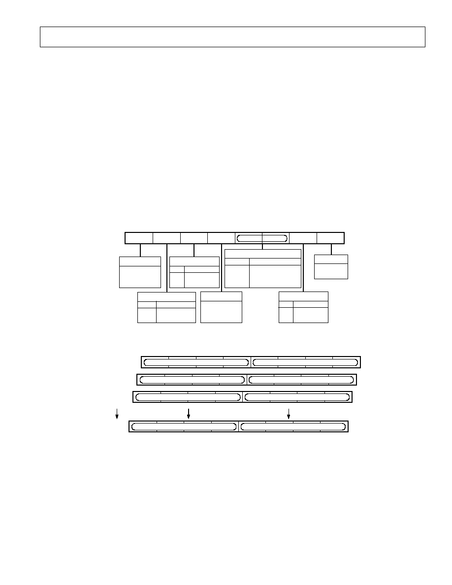
ADV7177/ADV7178
27
REV. A
MODE REGISTER 3 MR3 (MR37MR30)
(Address [SR4SR0] = 12H)
Mode Register 3 is an 8-bit-wide register.
Figure 41 shows the various operations under the control of
Mode Register 3.
MR3 BIT DESCRIPTION
Revision Code (MR30)
This bit is read only and indicates the revision of the device.
VBI Pass-Through (MR31)
This bit determines whether or not data in the vertical blanking
interval (VBI) is output to the analog outputs or blanked. VBI
data insertion is not available in Slave Mode 0. Also, if
BLANK
input control (TR03) is enabled, and VBI_Pass-Through is
enabled, TR03 has priority, i.e., VBI data insertion will not work.
Clock Output (MR33MR32)
These bits control the synchronous clock output signal. The
clock can be 27 MHz, 13.5 MHz or disabled, depending on the
values of these bits.
MR31
MR30
MR37
MR32
MR34
MR33
MR35
MR36
ZERO SHOULD
BE WRITTEN TO
THIS BIT
MR34
INPUT DEFAULT COLOR
0
INPUT COLOR
1
BLACK
MR36
VBI PASSTHROUGH
0 DISABLE
1 ENABLE
MR31
CLOCK OUTPUT
0
0
CLOCK OUTPUT OFF
0
1
13.5MHz OUTPUT
1
0
27MHz OUTPUT
1
1
CLOCK OUTPUT OFF
MR33-32
MR30
REV CODE
(READ ONLY)
ZERO SHOULD
BE WRITTEN TO
THIS BIT
MR37
OSD ENABLE
0 DISABLE
1 ENABLE
MR35
Figure 41. Mode Register 3
Y0
Cr0
Cb0
Y1
Cr1
Cb1
Cr7
Cb7
OSD
REG 0
OSD
REG 1
OSD
REG 2
OSD
REG 11
Figure 42. OSD Registers
OSD Enable (MR35)
A logic one in MR35 will enable the OSD function on
the ADV7177.
Input Default Color (MR36)
This bit determines the default output color from the DACs for
zero input data (or disconnected). A Logical "0" means that
the color corresponding to 00000000 will be displayed. A
Logical "1" forces the output color to black for 00000000
input video data.
Reserved (MR37)
Zero should be written to this bit.
OSD REGISTER 011
(Address [SR4SR0] = 13H1EH)
There are 12 OSD registers as shown in Figure 42. There are
four bits for each Y, Cb and Cr value, there are four zero added
to give the complete byte for each value loaded internally.
(Y0 = [Y0
3
, Y0
2
, Y0
1
, Y0
0
, 0, 0, 0, 0], Cb = [Cb
3
, Cb
2
, Cb
1
,
Cb
0
, 0, 0, 0, 0,], Cr = [Cr
3
, Cr
2
, Cr
1
, Cr
0
, 0, 0, 0, 0].)

ADV7177/ADV7178
28
REV. A
The ADV7177/ADV7178 is a highly integrated circuit containing
both precision analog and high speed digital circuitry. It has
been designed to minimize interference effects on the integrity
of the analog circuitry by the high speed digital circuitry. It is
imperative that these same design and layout techniques be applied
to the system level design so that high speed, accurate perfor-
mance is achieved. The "Recommended Analog Circuit Layout"
shows the analog interface between the device and monitor.
The layout should be optimized for lowest noise on the ADV7177/
ADV7178 power and ground lines by shielding the digital inputs
and providing good decoupling. The lead length between groups
of V
AA
and GND pins should by minimized to minimize induc-
tive ringing.
Ground Planes
The ground plane should encompass all ADV7177/ADV7178
ground pins, voltage reference circuitry, power supply bypass
circuitry for the ADV7177/ADV7178, the analog output traces, and
all the digital signal traces leading up to the ADV7177/ADV7178.
The ground plane is the board's common ground plane.
Power Planes
The ADV7177/ADV7178 and any associated analog circuitry
should have its own power plane, referred to as the analog
power plane (V
AA
). This power plane should be connected to
the regular PCB power plane (V
CC
) at a single point through a
ferrite bead. This bead should be located within three inches of
the ADV7177/ADV7178.
The metallization gap separating device power plane and board
power plane should be as narrow as possible to minimize the
obstruction to the flow of heat from the device into the gen-
eral board.
The PCB power plane should provide power to all digital logic
on the PC board, and the analog power plane should provide
power to all ADV7177/ADV7178 power pins and voltage refer-
ence circuitry.
Plane-to-plane noise coupling can be reduced by ensuring that
portions of the regular PCB power and ground planes do not
overlay portions of the analog power plane unless they can be
arranged so that the plane-to-plane noise is common-mode.
Supply Decoupling
For optimum performance, bypass capacitors should be installed
using the shortest leads possible, consistent with reliable operation,
APPENDIX 1
BOARD DESIGN AND LAYOUT CONSIDERATIONS
to reduce the lead inductance. Best performance is obtained
with 0.1
µF ceramic capacitor decoupling. Each group of V
AA
pins on the ADV7177/ADV7178 must have at least one 0.1
µF
decoupling capacitor to GND. These capacitors should be
placed as close to the device as possible.
It is important to note that while the ADV7177/ADV7178
contains circuitry to reject power supply noise, this rejection
decreases with frequency. If a high frequency switching power
supply is used, the designer should pay close attention to reduc-
ing power supply noise and consider using a three terminal voltage
regulator for supplying power to the analog power plane.
Digital Signal Interconnect
The digital inputs to the ADV7177/ADV7178 should be isolated
as much as possible from the analog outputs and other analog
circuitry. Also, these input signals should not overlay the analog
power plane.
Due to the high clock rates involved, long clock lines to the
ADV7177/ADV7178 should be avoided to reduce noise pickup.
Any active termination resistors for the digital inputs should be
connected to the regular PCB power plane (V
CC
) and not the
analog power plane.
Analog Signal Interconnect
The ADV7177/ADV7178 should be located as close to the
output connectors as possible to minimize noise pickup and
reflections due to impedance mismatch.
The video output signals should overlay the ground plane, not
the analog power plane, to maximize the high frequency power
supply rejection.
Digital inputs, especially pixel data inputs and clocking signals,
should never overlay any of the analog signal circuitry and
should be kept as far away as possible.
For best performance, the outputs should each have a 75
load
resistor connected to GND. These resistors should be placed as
close as possible to the ADV7177/ADV7178 as to minimize
reflections.
The ADV7177/ADV7178 should have no inputs left floating.
Any inputs that are not required should be tied to ground.
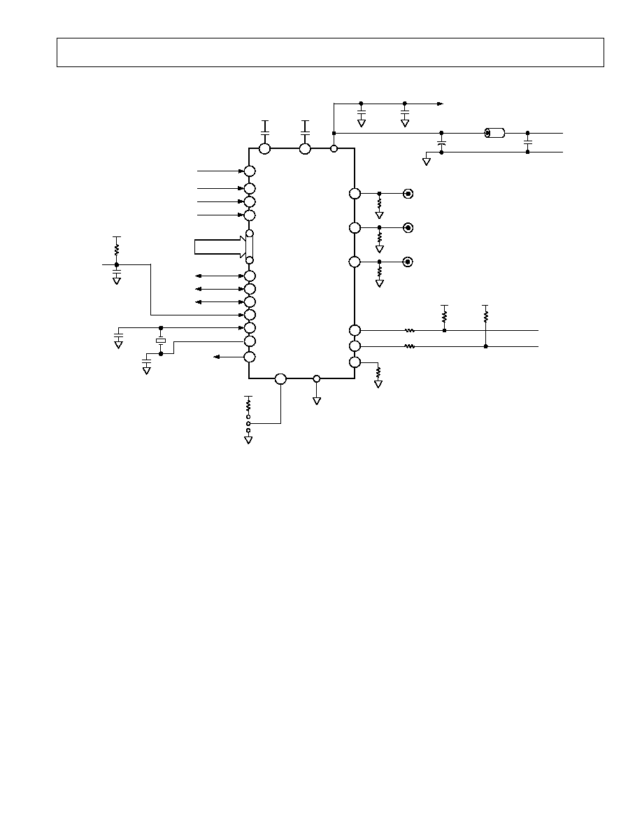
ADV7177/ADV7178
29
REV. A
0.1 F
+5V (V
AA
)
3741,
310, 1214
P15P0
32
5k
+5V (V
CC
)
150
24
5k
+5V (V
CC
)
MPU BUS
44
22
15
17
16
19, 21
29, 42
18
23
33
1, 20, 28, 30
0.1 F
0.01 F
POWER SUPPLY DECOUPLING
FOR EACH POWER SUPPLY GROUP
10 F
33 F
GND
L1
(FERRITE BEAD)
+5V
V
AA
+5V (V
AA
)
(V
CC
)
10k
+5V (V
AA
)
27MHz OR 13.5MHz
CLOCK OUTPUT
31
34
GND
ALSB
HSYNC
FIELD/
VSYNC
BLANK
RESET
CLOCK
R
SET
SDATA
SCLOCK
LUMA
V
REF
COMP
75
75
75
35
ADV7177/
ADV7178
"UNUSED
INPUTS
SHOULD BE
GROUNDED"
CHROMA
100
100
4k
+5V (V
AA
)
100nF
RESET
0.1 F
+5V (V
AA
)
11
36
OSD_EN
OSD_0
OSD_1
OSD_2
OSD
INPUTS
43
CLOCK
2
CLOCK/2
33pF
27MHz
XTAL
33pF
26
27
PIXEL
DATA
25
CVBS
Figure 43. Recommended Analog Circuit Layout
ADV7177/ADV7178
30
REV. A
The ADV7177/ADV7178 supports closed captioning, conform-
ing to the standard television synchronizing waveform for color
transmission. Closed captioning is transmitted during the
blanked active line time of Line 21 of the odd fields and Line
284 of even fields.
Closed captioning consists of a 7-cycle sinusoidal burst that is
frequency and phase locked to the caption data. After the clock
run-in signal, the blanking level is held for two data bits and is
followed by a Logic Level "1" start bit. 16 bits of data follow
the start bit. These consist of two 8-bit bytes, seven data bits
and one odd parity bit. The data for these bytes is stored in
closed captioning Data Registers 0 and 1.
The ADV7177/ADV7178 also supports the extended closed
captioning operation, which is active during even fields, and is
encoded on scan Line 284. The data for this operation is stored
in closed captioning extended Data Registers 0 and 1.
All clock run-in signals and timing to support closed caption-
ing on Lines 21 and 284 are generated automatically by the
ADV7177/ADV7178. All pixels inputs are ignored during
Lines 21 and 284.
APPENDIX 2
CLOSED CAPTIONING
FCC Code of Federal Regulations (CFR) 47 Section 15.119
and EIA608 describe the closed captioning information for
Lines 21 and 284.
The ADV7177/ADV7178 uses a single buffering method. This
means that the closed captioning buffer is only one byte deep,
therefore there will be no frame delay in outputting the closed
captioning data unlike other 2-byte deep buffering systems. The
data must be loaded at least one line before (Line 20 or Line
283) it is outputted on Line 21 and Line 284. A typical imple-
mentation of this method is to use
VSYNC to interrupt a
microprocessor, which will in turn load the new data (two bytes)
every field. If no new data is required for transmission you must
insert zeros in both the data registers; this is called NULLING.
It is also important to load "control codes," all of which are
double bytes on Line 21, or a TV will not recognize them. If
you have a message like "Hello World," which has an odd
number of characters, it is important to pad it out to an even
number to get "end of caption" 2-byte control code to land in
the same field.
12.91 s
S
T
A
R
T
P
A
R
I
T
Y
P
A
R
I
T
Y
D0D6
D0D6
10.003 s
33.764 s
50 IRE
40 IRE
FREQUENCY = F
SC
= 3.579545MHz
AMPLITUDE = 40 IRE
REFERENCE COLOR BURST
(9 CYCLES)
7 CYCLES
OF 0.5035 MHz
(CLOCK RUN-IN)
10.5 0.25 s
TWO 7-BIT + PARITY
ASCII CHARACTERS
(DATA)
27.382 s
BYTE 0
BYTE 1
Figure 44. Closed Captioning Waveform (NTSC)
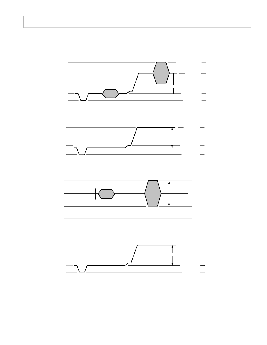
ADV7177/ADV7178
31
REV. A
APPENDIX 3
NTSC WAVEFORMS (WITH PEDESTAL)
130.8 IRE
100 IRE
7.5 IRE
0 IRE
40 IRE
PEAK COMPOSITE
REF WHITE
BLACK LEVEL
SYNC LEVEL
BLANK LEVEL
714.2mV
1268.1mV
1048.4mV
387.6mV
334.2mV
48.3mV
Figure 45. NTSC Composite Video Levels
100 IRE
7.5 IRE
0 IRE
40 IRE
REF WHITE
BLACK LEVEL
SYNC LEVEL
BLANK LEVEL
714.2mV
1048.4mV
387.6mV
334.2mV
48.3mV
Figure 46. NTSC Luma Video Levels
650mV
335.2mV
963.8mV
0mV
PEAK CHROMA
BLANK/BLACK LEVEL
286mVp-p
629.7mVp-p
PEAK CHROMA
Figure 47. NTSC Chroma Video Levels
100 IRE
7.5 IRE
0 IRE
40 IRE
REF WHITE
BLACK LEVEL
SYNC LEVEL
BLANK LEVEL
720.8mV
1052.2mV
387.5mV
331.4mV
45.9mV
Figure 48. NTSC RGB Video Levels
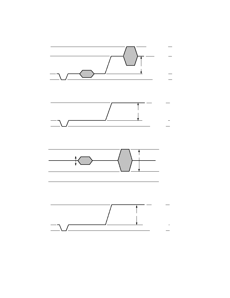
ADV7177/ADV7178
32
REV. A
NTSC WAVEFORMS (WITHOUT PEDESTAL)
130.8 IRE
100 IRE
0 IRE
40 IRE
PEAK COMPOSITE
REF WHITE
SYNC LEVEL
BLANK/BLACK LEVEL
714.2mV
1289.8mV
1052.2mV
338mV
52.1mV
Figure 49. NTSC Composite Video Levels
100 IRE
0 IRE
40 IRE
REF WHITE
SYNC LEVEL
BLANK/BLACK LEVEL
714.2mV
1052.2mV
338mV
52.1mV
Figure 50. NTSC Luma Video Levels
650mV
299.3mV
978mV
0mV
PEAK CHROMA
BLANK/BLACK LEVEL
286mVp-p
694.9mVp-p
PEAK CHROMA
Figure 51. NTSC Chroma Video Levels
100 IRE
0 IRE
40 IRE
REF WHITE
SYNC LEVEL
BLANK/BLACK LEVEL
715.7mV
1052.2mV
336.5mV
51mV
Figure 52. NTSC RGB Video Levels
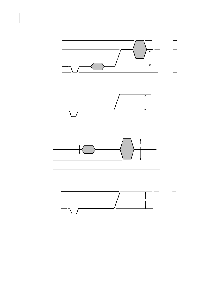
ADV7177/ADV7178
33
REV. A
PAL WAVEFORMS
1284.2mV
1047.1mV
350.7mV
50.8mV
PEAK COMPOSITE
REF WHITE
SYNC LEVEL
BLANK/BLACK LEVEL
696.4mV
Figure 53. PAL Composite Video Levels
1047mV
350.7mV
50.8mV
REF WHITE
SYNC LEVEL
BLANK/BLACK LEVEL
696.4mV
Figure 54. PAL Luma Video Levels
650mV
317.7mV
989.7mV
0mV
PEAK CHROMA
BLANK/BLACK LEVEL
300mVp-p
672mVp-p
PEAK CHROMA
Figure 55. PAL Chroma Video Levels
1050.2mV
351.8mV
51mV
REF WHITE
SYNC LEVEL
BLANK/BLACK LEVEL
698.4mV
Figure 56. PAL RGB Video Levels
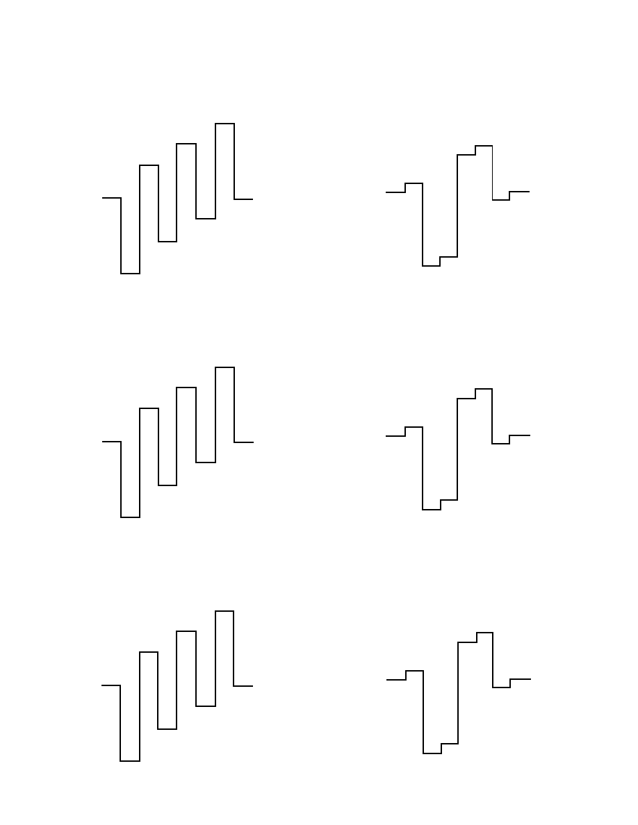
ADV7177/ADV7178
34
REV. A
BETACAM LEVEL
0mV
171mV
334mV
505mV
0mV
171mV
334mV
505mV
WHITE
YELLOW
CYAN
GREEN
MAGENTA
RED
BLUE
BLACK
Figure 57. NTSC 100% Color Bars No Pedestal U Levels
BETACAM LEVEL
0mV
158mV
309mV
467mV
0mV
158mV
309mV
467mV
WHITE
YELLOW
CYAN
GREEN
MAGENTA
RED
BLUE
BLACK
Figure 58. NTSC 100% Color Bars with Pedestal U Levels
SMPTE LEVEL
0mV
118mV
232mV
350mV
0mV
118mV
232mV
350mV
WHITE
YELLOW
CYAN
GREEN
MAGENTA
RED
BLUE
BLACK
Figure 59. PAL 1005 Color Bars U Levels
UV WAVEFORMS
BETACAM LEVEL
0mV
82mV
423mV
505mV
0mV
82mV
505mV
423mV
WHITE
YELLOW
CYAN
GREEN
MAGENTA
RED
BLUE
BLACK
Figure 60. NTSC 100% Color Bars No Pedestal V Levels
BETACAM LEVEL
0mV
76mV
391mV
467mV
0mV
76mV
467mV
391mV
WHITE
YELLOW
CYAN
GREEN
MAGENTA
RED
BLUE
BLACK
Figure 61. NTSC 100% Color Bars with Pedestal V Levels
SMPTE LEVEL
0mV
57mV
293mV
350mV
0mV
57mV
350mV
293mV
WHITE
YELLOW
CYAN
GREEN
MAGENTA
RED
BLUE
BLACK
Figure 62. PAL 100% Color Bars V Levels

ADV7177/ADV7178
35
REV. A
APPENDIX 4
REGISTER VALUES
The ADV7177/ADV7178 registers can be set depending on the
user standard required.
The following examples give the various register formats for
several video standards.
In each case the output is set to composite o/p with all DACs
powered up and with the
BLANK input control disabled. Addi-
tionally, the burst and color information are enabled on the
output and the internal color bar generator is switched off. In
the examples shown, the timing mode is set to Mode 0 in slave
format. TR02TR00 of the Timing Register 0 control the tim-
ing modes. For a detailed explanation of each bit in the
command registers, please turn to the Register Programming
section of the data sheet. TR07 should be toggled after setting
up a new timing mode. Timing Register 1 provides additional
control over the position and duration of the timing signals. In
the examples, this register is programmed in default mode.
NTSC (F
SC
= 3.5795454 MHz)
Address
Data
00Hex
Mode Register 0
04Hex
01Hex
Mode Register 1
00Hex
02Hex
Subcarrier Frequency Register 0
16Hex
03Hex
Subcarrier Frequency Register 1
7CHex
04Hex
Subcarrier Frequency Register 2
F0Hex
05Hex
Subcarrier Frequency Register 3
21Hex
06Hex
Subcarrier Phase Register
00Hex
07Hex
Timing Register 0
08Hex
08Hex
Closed Captioning Ext Register 0
00Hex
09Hex
Closed Captioning Ext Register 1
00Hex
0AHex
Closed Captioning Register 0
00Hex
0BHex
Closed Captioning Register 1
00Hex
0CHex
Timing Register 1
00Hex
0DHex
Mode Register 2
80Hex
0EHex
Pedestal Control Register 0
00Hex
0FHex
Pedestal Control Register 1
00Hex
10Hex
Pedestal Control Register 2
00Hex
11Hex
Pedestal Control Register 3
00Hex
12Hex
Mode Register 3
00Hex
PAL B, D, G, H, I (F
SC
= 4.43361875 MHz)
Address
Data
00Hex
Mode Register 0
01Hex
01Hex
Mode Register 1
00Hex
02Hex
Subcarrier Frequency Register 0
CBHex
03Hex
Subcarrier Frequency Register 1
8AHex
04Hex
Subcarrier Frequency Register 2
09Hex
05Hex
Subcarrier Frequency Register 3
2AHex
06Hex
Subcarrier Phase Register
00Hex
07Hex
Timing Register 0
08Hex
08Hex
Closed Captioning Ext Register 0
00Hex
09Hex
Closed Captioning Ext Register 1
00Hex
0AHex
Closed Captioning Register 0
00Hex
0BHex
Closed Captioning Register 1
00Hex
0CHex
Timing Register 1
00Hex
0DHex
Mode Register 2
80Hex
Address
Data
0EHex
Pedestal Control Register 0
00Hex
0FHex
Pedestal Control Register 1
00Hex
10Hex
Pedestal Control Register 2
00Hex
11Hex
Pedestal Control Register 3
00Hex
12Hex
Mode Register 3
00Hex
PAL M (F
SC
= 3.57561149 MHz)
Address
Data
00Hex
Mode Register 0
06Hex
01Hex
Mode Register 1
00Hex
02Hex
Subcarrier Frequency Register 0
A3Hex
03Hex
Subcarrier Frequency Register 1
EFHex
04Hex
Subcarrier Frequency Register 2
E6Hex
05Hex
Subcarrier Frequency Register 3
21Hex
06Hex
Subcarrier Phase Register
00Hex
07Hex
Timing Register 0
08Hex
08Hex
Closed Captioning Ext Register 0
00Hex
09Hex
Closed Captioning Ext Register 1
00Hex
0AHex
Closed Captioning Register 0
00Hex
0BHex
Closed Captioning Register 1
00Hex
0CHex
Timing Register 1
00Hex
0DHex
Mode Register 2
80Hex
0EHex
Pedestal Control Register 0
00Hex
0FHex
Pedestal Control Register 1
00Hex
10Hex
Pedestal Control Register 2
00Hex
11Hex
Pedestal Control Register 3
00Hex
12Hex
Mode Register 3
00Hex
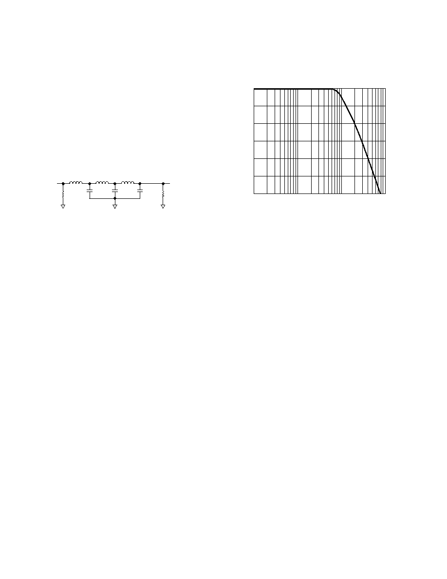
ADV7177/ADV7178
36
REV. A
If an output filter is required for the CVBS, Y, UV, Chroma and
RGB outputs of the ADV7177/ADV7178, the following filter in
Figure 63 can be used. Plots of the filter characteristics are
shown in Figure 64. An output filter is not required if the out-
puts of the ADV7177/ADV7178 are connected to an analog
monitor or an analog TV; however, if the output signals are
applied to a system where sampling is used (e.g., digital TV), a
filter is required to prevent aliasing.
L
1 H
L
2.7 H
L
0.68 H
R
75
R
75
C
470pF
C
330pF
C
56pF
IN
OUT
Figure 63. Output Filter
APPENDIX 5
OPTIONAL OUTPUT FILTER
FREQUENCY Hz
0
100
100k
100M
MAGNITUDE
dB
10M
1M
83.3
66.7
50
33.3
16.7
Figure 64. Output Filter Plot
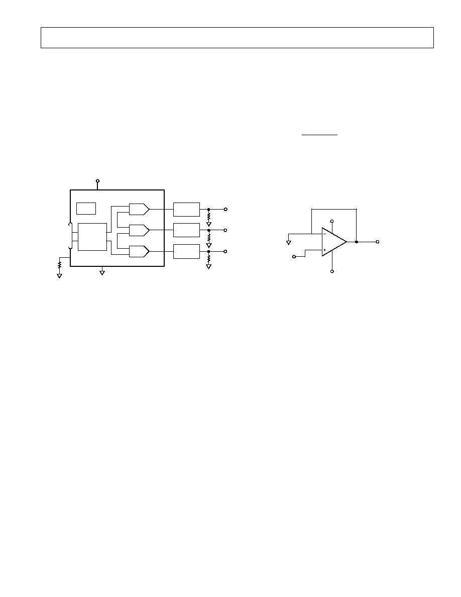
ADV7177/ADV7178
37
REV. A
For external buffering of the ADV7177/ADV7178 DAC out-
puts, the configuration in Figure 67 is recommended. This
configuration shows the DAC outputs running at half (18 mA)
their full current (34.7 mA) capability. This will allow the
ADV7177/ADV7178 to dissipate less power, the analog current is
reduced by 50% with a R
SET
of 300
and a R
LOAD
of 75
. This
mode is recommended for 3.3 volt operation as optimum perfor-
mance is obtained from the DAC outputs at 18 mA with a V
AA
of
3.3 volts. This buffer also adds extra isolation on the video
APPENDIX 6
OPTIONAL DAC BUFFERING
outputs, see buffer circuit in Figure 68. When calculating abso-
lute output full current and voltage, use the following equation:
V
OUT
= I
OUT
× R
LOAD
I
OUT
=
V
REF
× K
(
)
R
SET
K
= 4.2146 constant ,V
REF
= 1.235 V
ADV7177/ADV7178
V
REF
DIGITAL
CORE
PIXEL
PORT
300
R
SET
75
75
75
V
AA
OUTPUT
BUFFER
DAC A
OUTPUT
BUFFER
OUTPUT
BUFFER
DAC C
DAC B
Figure 65. Output DAC Buffering Configuration
AD8051
V
CC
+
V
CC
1
5
4
3
2
OUTPUT TO
TV MONITOR
INPUT/
OPTIONAL
FILTER O/P
Figure 68. Recommended Output DAC Buffer
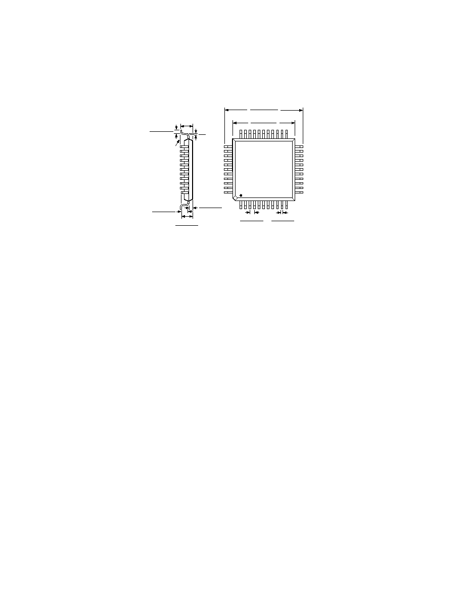
ADV7177/ADV7178
38
REV. A
OUTLINE DIMENSIONS
Dimensions shown in inches and (mm).
Plastic Quad Flatpack
(S-44)
0.548 (13.925)
0.546 (13.875)
TOP VIEW
(PINS DOWN)
1
33
34
44
11
12
23
22
0.033 (0.84)
0.029 (0.74)
0.398 (10.11)
0.390 (9.91)
0.016 (0.41)
0.012 (0.30)
0.083 (2.11)
0.077 (1.96)
0.040 (1.02)
0.032 (0.81)
0.040 (1.02)
0.032 (0.81)
SEATING
PLANE
0.096 (2.44)
MAX
0.037 (0.94)
0.025 (0.64)
8
0.8
PRINTED IN U.S.A.
C0022802/01 (rev. A)
Document Outline
- FEATURES
- APPLICATIONS
- GENERAL DESCRIPTION
- FUNCTIONAL BLOCK DIAGRAM
- SPECIFICATIONS
- 5 V SPECIFICATIONS
- 3.3 V SPECIFICATIONS
- 5 V DYNAMIC SPECIFICATIONS
- 3.3 V DYNAMIC SPECIFICATIONS
- 5 V TIMING SPECIFICATIONS
- 3.3 V TIMING SPECIFICATIONS
- ABSOLUTE MAXIMUM RATINGS
- ORDERING GUIDE
- PACKAGE THERMAL PERFORMANCE
- PIN CONFIGURATION
- PIN FUNCTION DESCRIPTIONS
- DATA PATH DESCRIPTION
- INTERNAL FILTER RESPONSE
- COLOR BAR GENERATION
- SQUARE PIXEL MODE
- COLOR SIGNAL CONTROL
- BURST SIGNAL CONTROL
- NTSC PEDESTAL CONTROL
- PIXEL TIMING DESCRIPTION
- 8-Bit YCrCb Mode
- 16-Bit YCrCb Mode
- OSD
- VIDEO TIMING DESCRIPTION
- Vertical Blanking Data Insertion
- Mode 0 (CCIR-656): Slave Option
- Mode 0 (CCIR-656): Master Option
- Mode 1: Slave Option HSYNC , BLANK , FIELD
- Mode 1: Master Option HSYNC , BLANK , FIELD
- Mode 2: Slave Option HSYNC , VSYNC , BLANK
- Mode 2: Master Option HSYNC , VSYNC , BLANK
- Mode 3: Master/Slave Option HSYNC , BLANK , FIELD
- POWER-ON RESET
- MPU PORT DESCRIPTION
- REGISTER ACCESSES
- REGISTER PROGRAMMING
- Subaddress Register (SR7
SR0)
- Register Select (SR5
SR0)
- MODE REGISTER 0 MR0 (MR07
MR00)
- (Address [SR4
SR0] = 00H)
- MR0 BIT DESCRIPTION
- Output Video Standard Selection (MR01
MR00)
- Pedestal Control (MR02)
- Luminance Filter Control (MR04
MR03)
- RGB Sync (MR05)
- Output Select (MR06)
- MODE REGISTER 1 MR1 (MR17
MR10)
- (Address (SR4
SR0) = 01H)
- MR1 BIT DESCRIPTION
- Interlaced Mode Control (MR10)
- Closed Captioning Field Selection (MR12
MR11)
- DAC Control (MR15
MR13)
- Color Bar Control (MR17)
- SUBCARRIER FREQUENCY REGISTER 3-0 (FSC3
FSC0)
- (Address [SR4
SR0] = 05H
02H)
- SUBCARRIER PHASE REGISTER (FP7
FP0)
- (Address [SR4
SR0] = 06H)
- TIMING REGISTER 0 (TR07
TR00)
- (Address [SR4
SR0] = 07H)
- TR0 BIT DESCRIPTION
- Master/Slave Control (TR00)
- Timing Mode Selection (TR02
TR01)
- BLANK Input Control (TR03)
- Luma Delay (TR05
TR04)
- Pixel Port Control (TR06)
- Timing Register Reset (TR07)
- CLOSED CAPTIONING EVEN FIELD DATA REGISTER 1
0 (CED15
CED0)
- (Subaddress [SR4
SR0] = 0B
0AH)
- TIMING REGISTER 1 (TR17
TR10)
- (Address [SR4
SR0] = 0CH)
- TR1 BIT DESCRIPTION
- HSYNC Width (TR11
TR10)
- HSYNC to FIELD/VSYNC Delay (TR13
TR12)
- HSYNC to FIELD Rising Edge Delay (TR15
TR14)
- VSYNC Width (TR15
TR14)
- HSYNC to Pixel Data Adjust (TR17
TR16)
- MODE REGISTER 2 MR2 (MR27
MR20)
- (Address [SR4-SR0] = 0DH)
- MR2 BIT DESCRIPTION
- Square Pixel Control (MR20)
- Active Video Line Duration (MR23)
- Chrominance Control (MR24)
- Burst Control (MR25)
- RGB/YUV Control (MR26)
- Low Power Control (MR27)
- NTSC PEDESTAL REGISTERS 3
0 (PCE15
0, PCO15
0)
- (Subaddress [SR4
SR0] = 11
0EH)
- MODE REGISTER 3 MR3 (MR37
MR30)
- (Address [SR4
SR0] = 12H)
- MR3 BIT DESCRIPTION
- Revision Code (MR30)
- VBI Pass-Through (MR31)
- Clock Output (MR33
MR32)
- OSD Enable (MR35)
- Input Default Color (MR36)
- Reserved (MR37)
- OSD REGISTER 0
11
- (Address [SR4
SR0] = 13H
1EH)
- APPENDIX 1
- BOARD DESIGN AND LAYOUT CONSIDERATIONS
- Ground Planes
- Power Planes
- Supply Decoupling
- Digital Signal Interconnect
- Analog Signal Interconnect
- APPENDIX 2
- APPENDIX 3
- NTSC WAVEFORMS (WITH PEDESTAL)
- NTSC WAVEFORMS (WITHOUT PEDESTAL)
- PAL WAVEFORMS
- UV WAVEFORMS
- APPENDIX 4
- REGISTER VALUES
- NTSC (FSC = 3.5795454 MHz)
- PAL B, D, G, H, I (FSC = 4.43361875 MHz)
- PAL M (FSC = 3.57561149 MHz)
- APPENDIX 5
- APPENDIX 6
- OUTLINE DIMENSIONS
- Plastic Quad Flatpack (S-44)
- TABLES
- Table I. Allowable Operating Conditions for ADV7177/ADV7178 IN 44-LEAD PQFP Package
- Table II. DAC Output Configuration Matrix