 | ÐлекÑÑоннÑй компоненÑ: ADV7178KS | СкаÑаÑÑ:  PDF PDF  ZIP ZIP |
Äîêóìåíòàöèÿ è îïèñàíèÿ www.docs.chipfind.ru
REV. 0
Information furnished by Analog Devices is believed to be accurate and
reliable. However, no responsibility is assumed by Analog Devices for its
use, nor for any infringements of patents or other rights of third parties
which may result from its use. No license is granted by implication or
otherwise under any patent or patent rights of Analog Devices.
a
ADV7177/ADV7178
One Technology Way, P.O. Box 9106, Norwood, MA 02062-9106, U.S.A.
Tel: 781/329-4700
World Wide Web Site: http://www.analog.com
Fax: 781/326-8703
© Analog Devices, Inc., 1998
Integrated Digital CCIR-601
to PAL/NTSC Video Encoder
FEATURES
ITU-R BT601/656 YCrCb to PAL/NTSC Video Encoder
High Quality 9-Bit Video DACs
Integral Nonlinearity <1 LSB at 9 Bits
NTSC-M, PAL-M/N, PAL-B/D/G/H/I
Single 27 MHz Crystal/Clock Required ( 2 Oversampling)
75 dB Video SNR
32-Bit Direct Digital Synthesizer for Color Subcarrier
Multistandard Video Output Support:
Composite (CVBS)
Component S-Video (Y/C)
Component YUV and RGB
Video Input Data Port Supports:
CCIR-656 4:2:2 8-Bit Parallel Input Format
4:2:2 16-Bit Parallel Input Format
SMPTE 170M NTSC-Compatible Composite Video
ITU-R BT.470 PAL-Compatible Composite Video
Full Video Output Drive or Low Signal Drive Capability
34.7 mA max into 37.5 (Doubly-Terminated 75R)
5 mA min with External Buffers
Programmable Simultaneous Composite and S-VHS
(VHS) Y/C or RGB (SCART)/YUV Video Outputs
Programmable Luma Filters (Low-Pass/Notch/Extended)
Programmable VBI (Vertical Blanking Interval)
Programmable Subcarrier Frequency and Phase
Programmable LUMA Delay
Individual ON/OFF Control of Each DAC
CCIR and Square Pixel Operation
Color Signal Control/Burst Signal Control
Interlaced/Noninterlaced Operation
Complete On-Chip Video Timing Generator
OSD Support (AD7177 Only)
Programmable Multimode Master/Slave Operation
Macrovision Antitaping Rev 7.01 (ADV7178 Only)**
Closed Captioning Support
Onboard Voltage Reference
2-Wire Serial MPU Interface (I
2
C
®
Compatible)
Single Supply +5 V or +3 V Operation
Small 44-Lead PQFP Package
Synchronous 27 MHz/13.5 MHz Clock O/P
APPLICATIONS
MPEG-1 and MPEG-2 Video, DVD, Digital Satellite/
Cable Systems (Set Top Boxes/IRDs), Digital TVs,
CD Video/Karaoke, Video Games, PC Video/Multimedia
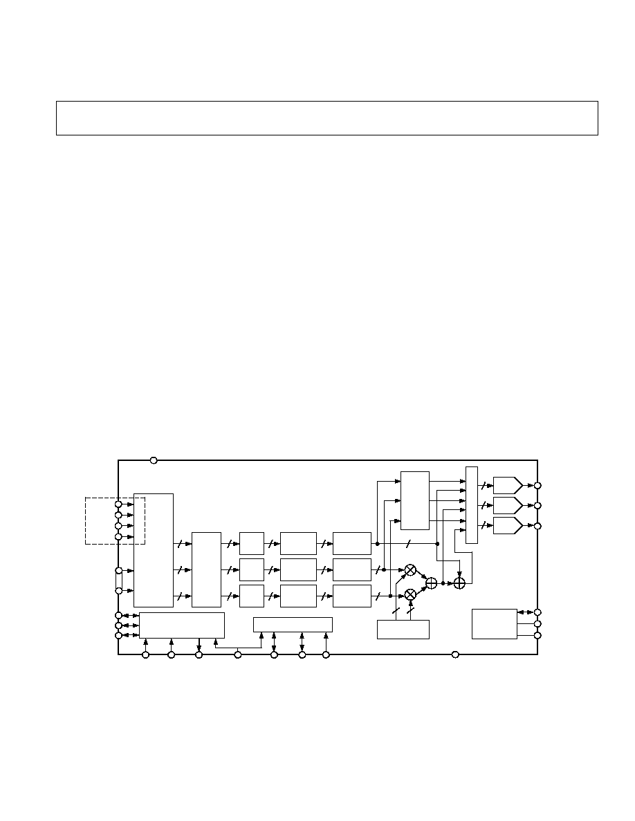
GENERAL DESCRIPTION
The ADV7177/ADV7178 is an integrated digital video encoder
that converts Digital CCIR-601 4:2:2 8- or 16-bit component
video data into a standard analog baseband television signal
FUNCTIONAL BLOCK DIAGRAM
OSD_EN
OSD_0
OSD_1
OSD_2
P7P0
P15P8
COLOR
DATA
ADV7177
ONLY
4:2:2 TO
4:4:4
INTER-
POLATOR
8
8
8
8
ADD
BURST
8
INTER-
POLATOR
8
V
LOW-PASS
FILTER
9
9
9
9
9
SIN/COS
DDS BLOCK
YUV TO
RBG
MATRIX
M
U
L
T
I
P
L
E
X
E
R
9
9
9
9-BIT
DAC
9-BIT
DAC
9-BIT
DAC
DAC C (PIN 26)
DAC B (PIN 27)
DAC A (PIN 31)
ADV7177/ADV7178
VOLTAGE
REFERENCE
CIRCUIT
VIDEO TIMING
GENERATOR
I
2
C MPU PORT
CLOCK
CLOCK
CLOCK/2
RESET
SCLOCK SDATA ALSB
GND
V
REF
R
SET
COMP
V
AA
HSYNC
FIELD/
VSYNC
BLANK
8
ADD
BURST
8
INTER-
POLATOR
8
U
LOW-PASS
FILTER
8
ADD
SYNC
8
INTER-
POLATOR
8
Y
LOW-PASS
FILTER
YCrCb
TO
YUV
MATRIX
*Protected by U.S. Patent Numbers 5,343,196 and 5,442,355 and other intellectual property rights.
**This device is protected by U.S. Patent Numbers 4,631,603, 4,577,216, 4,819,098 and other intellectual property rights. The Macrovision anticopy process is
licensed for noncommercial home use only, which is its sole intended use in the device. Please contact sales office for latest Macrovision version available.
NOTE: ITU-R and CCIR are used interchangeably in this document (ITU-R has replaced CCIR recommendations).
I
2
C is a registered trademark of Philips Corporation.
(Continued on page 11)

2
REV. 0
ADV7177/ADV7178SPECIFICATIONS
(V
AA
= +5 V 5%
1
, V
REF
= 1.235 V, R
SET
= 300
. All specifications T
MIN
to T
MAX
2
unless otherwise noted.)
Parameter
Conditions
1
Min
Typ
Max
Units
STATIC PERFORMANCE
3
Resolution (Each DAC)
9
Bits
Accuracy (Each DAC)
Integral Nonlinearity
±
1.0
LSB
Differential Nonlinearity
Guaranteed Monotonic
±
1.0
LSB
DIGITAL INPUTS
3
Input High Voltage, V
INH
2
V
Input Low Voltage, V
INL
0.8
V
Input Current, I
IN
4
V
IN
= 0.4 V or 2.4 V
±
1
µ
A
Input Current, I
IN
5
V
IN
= 0.4 V or 2.4 V
±
50
µ
A
Input Capacitance, C
IN
10
pF
DIGITAL OUTPUTS
3
Output High Voltage, V
OH
I
SOURCE
= 400
µ
A
2.4
V
Output Low Voltage, V
OL
I
SINK
= 3.2 mA
0.4
V
Three-State Leakage Current
10
µ
A
Three-State Output Capacitance
10
pF
ANALOG OUTPUTS
3
Output Current
6
R
SET
= 300
, R
L
= 75
16.5
17.35
18.5
mA
Output Current
7
5
mA
DAC-to-DAC Matching
0.6
5
%
Output Compliance, V
OC
0
+1.4
V
Output Impedance, R
OUT
15
k
Output Capacitance, C
OUT
I
OUT
= 0 mA
30
pF
VOLTAGE REFERENCE
3
Reference Range, V
REF
I
VREFOUT
= 20
µ
A
1.112
1.235
1.359
V
POWER REQUIREMENTS
3, 8
V
AA
4.75
5.0
5.25
V
Low Power Mode
I
DAC
(max)
9
62
mA
I
DAC
(min)
9
25
mA
I
CCT
10
100
150
mA
Power Supply Rejection Ratio
COMP = 0.1
µ
F
0.01
0.5
%/%
NOTES
1
1
The max/min specifications are guaranteed over this range. The max/min values are typical over 4.75 V to 5.25 V.
1
2
Temperature range T
MIN
to T
MAX
: 0
°
C to +70
°
C.
1
3
Guaranteed by characterization.
1
4
All digital input pins except pins
RESET, OSD0 and CLOCK.
1
5
Excluding all digital input pins except pins
RESET, OSD0 and CLOCK.
1
6
Full
drive into 75
load.
1
7
Minimum drive current (used with buffered/scaled output load).
1
8
Power measurements are taken with Clock Frequency = 27 MHz. Max T
J
= 110
°
C.
1
9
I
DAC
is the total current (min corresponds to 5 mA output per DAC, max corresponds to 18.5 mA output per DAC) to drive all three DACs. Turning off individual
DACs reduces I
DAC
correspondingly.
10
I
CCT
(Circuit Current) is the continuous current required to drive the device.
Specifications subject to change without notice.
5 V SPECIFICATIONS

3
REV. 0
ADV7177/ADV7178
Parameter
Conditions
1
Min
Typ
Max
Units
STATIC PERFORMANCE
3
Resolution (Each DAC)
9
Bits
Accuracy (Each DAC)
Integral Nonlinearity
±
0.5
LSB
Differential Nonlinearity
Guaranteed Monotonic
±
0.5
LSB
DIGITAL INPUTS
Input High Voltage, V
INH
2
V
Input Low Voltage, V
INL
0.8
V
Input Current, I
IN
3, 4
V
IN
= 0.4 V or 2.4 V
±
1
µ
A
Input Current, I
IN
3,
5
V
IN
= 0.4 V or 2.4 V
±
50
µ
A
Input Capacitance, C
IN
10
pF
DIGITAL OUTPUTS
Output High Voltage, V
OH
I
SOURCE
= 400
µ
A
2.4
V
Output Low Voltage, V
OL
I
SINK
= 3.2 mA
0.4
V
Three-State Leakage Current
3
10
µ
A
Three-State Output Capacitance
3
10
pF
ANALOG OUTPUTS
3
Output Current
6, 7
R
SET
= 300
, R
L
= 75
16.5
17.35
18.5
mA
Output Current
8
5
mA
DAC-to-DAC Matching
2.0
%
Output Compliance, V
OC
0
+1.4
V
Output Impedance, R
OUT
15
k
Output Capacitance, C
OUT
I
OUT
= 0 mA
30
pF
POWER REQUIREMENTS
3, 9
V
AA
3.0
3.3
3.6
V
Normal Power Mode
I
DAC
(max)
10
R
SET
= 300
, R
L
= 150
113
116
mA
I
DAC
(min)
10
15
mA
I
CCT
9
45
mA
Low Power Mode
I
DAC
(max)
10
60
mA
I
DAC
(min)
10
25
mA
I
CCT
11
45
mA
Power Supply Rejection Ratio
COMP = 0.1
µ
F
0.01
0.5
%/%
NOTES
1
1
The max/min specifications are guaranteed over this range. The max/min values are typical over 3.0 V to 3.6 V.
1
2
Temperature range T
MIN
to T
MAX
: 0
°
C to +70
°
C.
1
3
Guaranteed by characterization.
1
4
All digital input pins except pins
RESET, OSD0 and CLOCK.
1
5
Excluding all digital input pins except pins
RESET, OSD0 and CLOCK.
1
6
Full
drive into 75
load.
1
7
DACs can output 35 mA typically at 3.3 V (R
SET
= 150
and R
L
= 75
), optimum performance obtained at 18 mA DAC current (R
SET
= 300
and R
L
= 150
).
1
8
Minimum drive current (used with buffered/scaled output load).
1
9
Power measurements are taken with Clock Frequency = 27 MHz. Max T
J
= 110
°
C.
10
I
DAC
is the total current (min corresponds to 5 mA output per DAC, max corresponds to 38 mA output per DAC) to drive all three DACs. Turning off individual
DACs reduces I
DAC
correspondingly.
11
I
CCT
(Circuit Current) is the continuous current required to drive the device.
Specifications subject to change without notice.
3.3 V SPECIFICATIONS
(V
AA
= +3.0 V3.6 V
1
, V
REF
= 1.235 V, R
SET
= 300
. All specifications T
MIN
to T
MAX
2
unless otherwise noted.)
4
REV. 0
ADV7177/ADV7178SPECIFICATIONS
Parameter
Conditions
1
Min
Typ
Max
Units
Filter Characteristics
Luma Bandwidth
3
(Low-Pass Filter)
NTSC Mode
Stopband Cutoff
>54 dB Attenuation
7.0
MHz
Passband Cutoff F
3 dB
>3 dB Attenuation
4.2
MHz
Chroma Bandwidth
NTSC Mode
Stopband Cutoff
>40 dB Attenuation
3.2
MHz
Passband Cutoff F
3 dB
>3 dB Attenuation
2.0
MHz
Luma Bandwidth
3
(Low-Pass Filter)
PAL MODE
Stopband Cutoff
>50 dB Attenuation
7.4
MHz
Passband Cutoff F
3 dB
>3 dB Attenuation
5.0
MHz
Chroma Bandwidth
PAL MODE
Stopband Cutoff
>40 dB Attenuation
4.0
MHz
Passband Cutoff F
3 dB
>3 dB Attenuation
2.4
MHz
Differential Gain
4
Lower Power Mode
2.0
%
Differential Phase
4
Lower Power Mode
1.5
Degrees
SNR
4
(Pedestal)
RMS
75
dB rms
Peak Periodic
70
dB p-p
SNR
4
(Ramp)
RMS
57
dB rms
Peak Periodic
56
dB p-p
Hue Accuracy
4
1.2
Degrees
Color Saturation Accuracy
4
1.4
%
Chroma Nonlinear Gain
4
Referenced to 40 IRE
1.0
±
%
Chroma Nonlinear Phase
4
NTSC
0.4
±
Degrees
PAL
0.6
±
Degrees
Chroma/Luma Intermod
4
Referenced to 714 mV (NTSC)
0.2
±
%
Referenced to 700 mV (PAL)
0.2
±
%
Chroma/Luma Gain Ineq
4
0.6
±
%
Chroma/Luma Delay Ineq
4
2.0
ns
Luminance Nonlinearity
4
1.2
±
%
Chroma AM Noise
4
64
dB
Chroma PM Noise
4
62
dB
NOTES
1
The max/min specifications are guaranteed over this range. The max/min values are typical over 4.75 V to 5.25 V.
2
Temperature range T
MIN
to T
MAX
: 0
°
C to +70
°
C.
3
These specifications are for the low-pass filter only and guaranteed by design. For other internal filters, see Figure 5.
4
Guaranteed by characterization.
Specifications subject to change without notice.
5 V DYNAMIC SPECIFICATIONS
1
(V
AA
= +4.75 V 5.25 V
1
, V
REF
= 1.235 V, R
SET
= 300 . All specifications T
MIN
to T
MAX
2
unless otherwise noted.)

5
REV. 0
ADV7177/ADV7178
Parameter
Conditions
1
Min
Typ
Max
Units
Filter Characteristics
Luma Bandwidth
3
(Low-Pass Filter)
NTSC Mode
Stopband Cutoff
>54 dB Attenuation
7.0
MHz
Passband Cutoff F
3 dB
>3 dB Attenuation
4.2
MHz
Chroma Bandwidth
NTSC Mode
Stopband Cutoff
>40 dB Attenuation
3.2
MHz
Passband Cutoff F
3 dB
>3 dB Attenuation
2.0
MHz
Luma Bandwidth
3
(Low-Pass Filter)
PAL MODE
Stopband Cutoff
>50 dB Attenuation
7.4
MHz
Passband Cutoff F
3 dB
>3 dB Attenuation
5.0
MHz
Chroma Bandwidth
PAL MODE
Stopband Cutoff
>40 dB Attenuation
4.0
MHz
Passband Cutoff F
3 dB
>3 dB Attenuation
2.4
MHz
Differential Gain
4
Normal Power Mode
1.0
%
Differential Phase
4
Normal Power Mode
1.0
Degrees
SNR
4
(Pedestal)
RMS
70
dB rms
Peak Periodic
64
dB p-p
SNR
4
(Ramp)
RMS
56
dB rms
Peak Periodic
54
dB p-p
Hue Accuracy
4
1.2
Degrees
Color Saturation Accuracy
4
1.4
%
Luminance Nonlinearity
4
1.4
±
%
Chroma AM Noise
4
NTSC
64
dB
Chroma PM Noise
4
NTSC
62
dB
Chroma AM Noise
4
PAL
64
dB
Chroma PM Noise
4
PAL
62
dB
NOTES
1
The max/min specifications are guaranteed over this range. The max/min values are typical over 3.0 V to 3.6 V.
2
Temperature range T
MIN
to T
MAX
: 0
°
C to +70
°
C.
3
These specifications are for the low-pass filter only and guaranteed by design. For other internal filters, see Figure 5.
4
Guaranteed by characterization.
Specifications subject to change without notice.
3.3 V DYNAMIC SPECIFICATIONS
1
(V
AA
= +3.0 V 3.6 V
1
, V
REF
= 1.235 V, R
SET
= 300
. All specifications T
MIN
to T
MAX
2
unless otherwise noted.)