Äîêóìåíòàöèÿ è îïèñàíèÿ www.docs.chipfind.ru
REV. 0
a
Information furnished by Analog Devices is believed to be accurate and
reliable. However, no responsibility is assumed by Analog Devices for its
use, nor for any infringements of patents or other rights of third parties that
may result from its use. No license is granted by implication or otherwise
under any patent or patent rights of Analog Devices.
One Technology Way, P.O. Box 9106, Norwood, MA 02062-9106, U.S.A.
Tel: 781/329-4700
www.analog.com
Fax: 781/326-8703
© Analog Devices, Inc., 2002
ADV7183
Advanced Video Decoder with 10-Bit ADC
and Component Input Support
ADLLT is a trademark and ADV is a registered trademark of Analog Devices, Inc.
FEATURES
Analog Video to Digital YCrCb Video Decoder:
NTSC-(M/N), PAL-(B/D/G/H/I/M/N)
ADV
®
7183 Integrates Two 10-Bit Accurate ADCs
Clocked from a Single 27 MHz Crystal
Dual Video Clocking Schemes:
Line-Locked Clock Compatible (LLC)
Adaptive Digital Line Length Tracking (ADLLTTM)
Three-Line Chroma Comb Filter
Real-Time Clock and Status Information Output
Integrated AGC (Automatic Gain Control) and Clamping
Multiple Programmable Analog Input Formats:
CVBS (Composite Video)
SVHS (Y/C)
YCrCb Component (VESA, MII, SMPTE, and BetaCom)
6 Analog Input Video Channels
Automatic NTSC/PAL Identification
Differential Mode Video Input
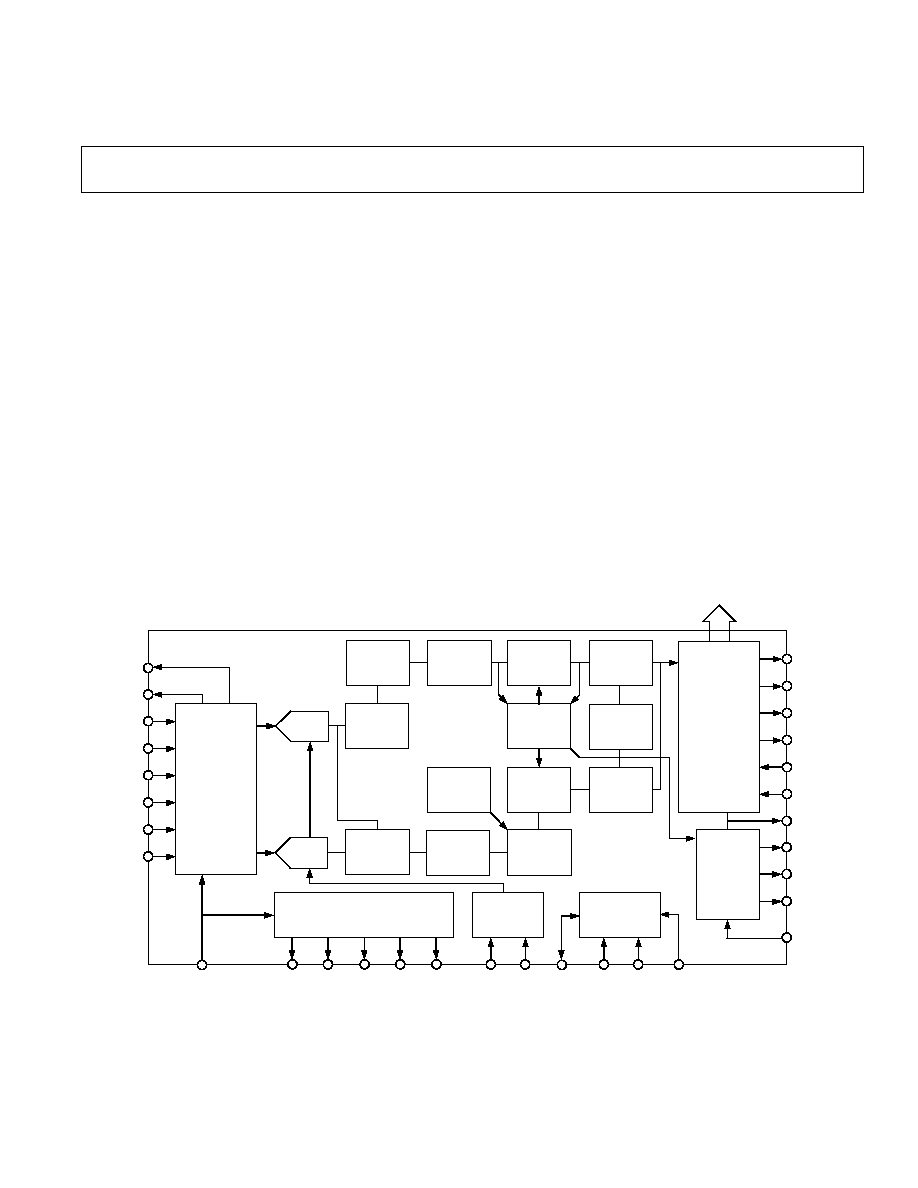
FUNCTIONAL BLOCK DIAGRAM
ISO
REFOUT
AIN1
AIN2
AIN3
AIN4
AIN5
AIN6
ANALOG I/P
MULTIPLEXING
AUTOMATIC
GAIN
CONTROL
(AGC)
CLAMP AND
DC RESTORE
10-BIT
ADC
LUMA
ANTIALIAS
LPF
SHAPING
AND
NOTCH LPF
PEAKING
HPF/LPF
RESAMPLING
AND
HORIZONTAL
SCALING
CHROMA
COMB
FILTER
SYNC
DETECTION
ADV7183
RESAMPLING
AND
HORIZONTAL
SCALING
CHROMA
ANTIALIAS
LPF
SHAPING
LPF
SWITCH
LUMA
DELAY
BLOCK
2H LINE
MEMORY
SUB-
CARRIER
RECOVERY
DTO
10-BIT
ADC
27MHz
VIDEO TIMING AND
CONTROL BLOCK
27MHz XTAL
OSCILLATOR
BLOCK
PWRDN
HSYNC FIELD VSYNC HREF
VREF
CLOCK
CLOCK
AFF
HFF/QCLK
AEF
DV
RD
OE
FIFO CONTROL
BLOCK
AND
PIXEL
OUTPUT
FORMATTER
LLC
SYNTHESIS
WITH LINE-
LOCKED
OUTPUT
CLOCK
I
2
C-COMPATIBLE
INTERFACE PORT
SDATA SCLOCK
RESET
ALSB
GL/CLKIN
LLC1
LLC2
LLCREF
ELPF
P15P0
PIXEL
O/P PORT
Digital Output Formats 16-Bit Wide Bus):
YCrCb (4:2:2 or 4:1:1)
CCIR601/CCIR656 8-Bit or 16-Bit
0.5 V to 2.0 V p-p Input Range
Differential Gain, 0.4% Typ
Differential Phase, 0.6
o
Typ
Programmable Video Controls:
Peak White/Hue/Brightness/Saturation/Contrast
APPLICATIONS
Security Systems
Projectors
Digital Televisions
DVD-RAM Recorders and Players
PDP Displays
Video Decoders
Hybrid Analog/Digital Set-Top Boxes
(continued on page 9)

REV. 0
2
ADV7183SPECIFICATIONS
1
(V
AA
= 4.75 V to 5.25 V, V
DD
= 3.2 V to 3.5 V, V
DDIO
= 3.15 V to 3.5 V, T
MIN
to T
MAX
2
,
unless otherwise noted.)
Parameter
Min
Typ
Max
Unit
Test Conditions
STATIC PERFORMANCE
Resolution (each ADC)
10
Bits
Accuracy (each ADC)
Integral Nonlinearity
3
±0.25
±0.5
LSB
BSL, 2 V Input Range to ADC
Differential Nonlinearity
3
±0.08
±0.17
LSB
2 V Input Range to ADC
DIGITAL INPUTS
3
Input High Voltage, V
INH
2
V
Input Low Voltage, V
INL
0.8
V
Input Current, I
IN
10
+10
µA
Input Capacitance, C
IN
10
pF
DIGITAL OUTPUTS
3
Output High Voltage, V
OH
2.4
V
I
SOURCE
= 3.2 mA
Output Low Voltage, V
OL
0.4
V
I
SINK
= 0.4 mA
High Impedance Leakage Current
10
µA
Output Capacitance
30
pF
VOLTAGE REFERENCE
3
Reference Range, V
REFOUT
2.15
2.2
2.25
V
I
VREFOUT
= 0
µA
POWER REQUIREMENTS
Digital Power Supply, V
DD
3.2
3.3
3.5
V
Digital IO Power Supply, V
DDIO
3.15
3.3
3.5
V
Analog Power Supply, V
AA
4.75
5.0
5.25
V
Digital Supply Current, I
DD
125
165
mA
Digital IO Supply Current, I
DDIO
7
mA
Analog Supply Current, I
AA
4
150
180
mA
Power-Up Time
1
Field
Sleep Mode until Powered Up
NOTES
1
The max/min specifications are guaranteed over this range. The max/min values are typical over V
AA
= 4.75 V to 5.25 V, V
DD
= 3.2 to 3.5 V, and V
DDIO
= 3.15 V to
3.5 V range.
2
Temperature range T
MIN
to T
MAX
= 0
°C to 70°C
3
Guaranteed by characterization.
4
I
AA
is total analog current taken by AVDD supply pins.
Specifications subject to change without notice.

REV. 0
ADV7183
3
VIDEO PERFORMANCE SPECIFICATIONS
1, 2
Parameter
Min
Typ
Max
Unit
Test Conditions
NONLINEAR SPECIFICATIONS
2
Differential Phase
0.6
Degree
CVBS, Comb/No Comb
Differential Gain
0.7
%
CVBS, Comb/No Comb
Luma Nonlinearity
1.0
%
NOISE SPECIFICATIONS
2
SNR (Ramp)
61
54
dB
CVBS
Analog Front End Channel Crosstalk
63
dB
S-Video/YUV, Single-Ended
Analog Front End Channel Crosstalk
63
dB
S-Video/YUV, Differential-Ended
LOCK TIME AND JITTER
SPECIFICATIONS
2
Horizontal Lock Time
50
Lines
TV/VCR mode
Horizontal Recovery Time
50
Lines
Horizontal Lock Range
±5
%
Line Length Variation Over Field
±1
%
VCR Mode/Surveillance Mode
Line Length Variation Over Field
±1
%
TV Mode
HLock Lost Declared
10
HSync
TV Mode, Number of Missing HSyncs
HLock Lost Declared
20
HSync
VCR/Surveillance Mode, Number of
Missing HSyncs
Vertical Lock Time
2
VSync
First Lock into Video Signal
VLock Lost Declared
1
VSync
All Modes, Number of Missing VSyncs
F
SC
Subcarrier Lock Range
±400
Hz
NTSC/PAL
Color Lock Time
50
Lines
HLock to Color Lock Time
LLC Clock Jitter (Short Time Jitter)
1
ns
RMS Clock Jitter
LLC Clock Jitter (Frame Jitter)
37
ns
RMS Clock Jitter
CHROMA-SPECIFIC
SPECIFICATIONS
2
Hue Accuracy
1.0
Degree
Color Saturation Accuracy
1.0
%
Color Gain Control Range
6
+18
dB
S-Video, YUV, Overall CGC Range
(Analog and Digital)
Analog Color Gain Range
6
+6
dB
S-Video, YUV
Digital Color Gain Range
0
12
dB
CVBS, S-Video, YUV
Chroma Amplitude Error
0.1
%
Chroma Phase Error
0
Degree
Chroma Luma Intermodulation
0.1
%
LUMA-SPECIFIC SPECIFICATIONS
2
Luma Brightness Accuracy
1.0
%
Video Input Range = 1.0 V p-p
Luma Contrast Accuracy
1.0
%
Video Input Range = 1.0 V p-p
NOTES
1
The max/min specifications are guaranteed over this range. The max/min values are typical over V
AA
= 4.75 V to 5.25 V, V
DD
= 3.2 to 3.5 V, and V
DDIO
= 3.15 V to
3.5 V range.
2
Guaranteed by characterization.
3
Temperature range T
MIN
to T
MAX
= 0
°C to 70°C
Specifications subject to change without notice.
(V
AA
= 4.75 V to 5.25 V, V
DD
= 3.2 V to 3.5 V, V
DDIO
= 3.15 V to 3.5 V,
T
MIN
to T
MAX
3
, unless otherwise noted.)

REV. 0
4
ADV7183
TIMING SPECIFICATIONS
1
Parameter
Min
Typ
Max
Unit
Test Conditions
SYSTEM CLOCK AND CRYSTAL
Nominal Frequency
27
MHz
I
2
C PORT
2
SCL Clock Frequency
0
400
kHz
SCL Min Pulsewidth High, t
1
0.6
µs
SCL Min Pulsewidth Low, t
2
1.3
µs
Hold Time (Start Condition), t
3
0.6
µs
Setup Time (Start Condition), t
4
0.6
µs
Data Setup Time, t
5
100
ns
SCL/SDA Rise Time, t
6
300
ns
SCL/SDA Fall Time, t
7
300
ns
Setup Time (Stop Condition), t
8
0.6
µs
RESET FEATURE
Reset Pulse Input Width
74
ns
CLOCK OUTPUTS
3
LLC1 Cycle Time, t
9
37
ns
CCIR601 Mode 27 MHz
LLC1 Cycle Time, t
9
33.9
ns
PAL Square Pixel Mode 29.5 MHz
LLC1 Cycle Time, t
9
40.8
ns
NTSC Square Pixel Mode 24.5 MHz
LLC1 Min Low Period, t
10
18
ns
CCIR601 Mode 27 MHz
LLC1 Min High Period, t
11
18
ns
CCIR601 Mode 27 MHz
LLC1 Falling to LLCREF Falling, t
12
4
ns
LLC1 Falling to LLCREF Rising, t
13
6
ns
LLC1 Rising to LLC2 Rising, t
14
3
5
ns
LLC1 Rising to LLC2 Falling, t
15
1
3
ns
CLKIN Cycle Time, t
18
37
ns
SCAPI and CAPI Modes
DATA AND CONTROL OUTPUT
Data Output Hold Time, t
17
26
ns
LLC Mode
Data Output Access Time, t
16
30
33
ns
LLC Mode
Data Output Access Time, t
19
20
25
ns
SCAPI and CAPI Modes
Data Output Hold Time, t
20
6
11
ns
SCAPI and CAPI Modes
Propagation Delay to High Z, t
21
5
8
ns
Max Output Enable Access Time, t
22
8
11
ns
Min Output Enable Access Time, t
23
2
5
ns
NOTES
1
The max/min specifications are guaranteed over this range. The max/min values are typical over V
AA
= 4.75 V to 5.25 V, V
DD
= 3.2 to 3.5 V, and V
DDIO
= 3.15 V to
3.5 V range.
2
Temperature Range T
MIN
to T
MAX
= 0
°C to 70°C
3
Guaranteed by characterization.
Specifications subject to change without notice.
(V
AA
= 4.75 V to 5.25 V, V
DD
= 3.2 V to 3.5 V, V
DDIO
= 3.15 V to 3.5 V, T
MIN
to T
MAX
2
,
unless otherwise noted.)
ANALOG FRONT END SPECIFICATIONS
1
Parameter
Min
Typ
Max
Unit
Test Conditions
CLAMP CIRCUITRY
External Clamp Capacitor
0.1
µF
Input Impedance
10
M
Clamp Switched Off
Voltage Clamp Level
1.4
V
Clamp Source Current
3
µA
Signal Already Clamped (Fine Clamping)
Sink Current
3
µA
Signal Already Clamped (Fine Clamping)
Source Current
0.9
mA
Acquire Mode (Fast Clamping)
Clamp Sink Current
0.9
mA
Acquire Mode (Fast Clamping)
NOTES
1
The max/min specifications are guaranteed over this range. The max/min values are typical over V
AA
= 4.75 V to 5.25 V, V
DD
= 3.2 to 3.5 V, and V
DDIO
= 3.15 V to
3.5 V range.
2
Temperature range T
MIN
to T
MAX
= 0
°C to 70°C
Specifications subject to change without notice.
(V
AA
= 4.75 V to 5.25 V, V
DD
= 3.2 V to 3.5 V, V
DDIO
= 3.15 V to 3.5 V, T
MIN
to T
MAX
2
,
unless otherwise noted.)
REV. 0
ADV7183
5
SDATA
SCLOCK
t
3
t
2
t
6
t
1
t
7
t
5
t
4
t
3
t
8
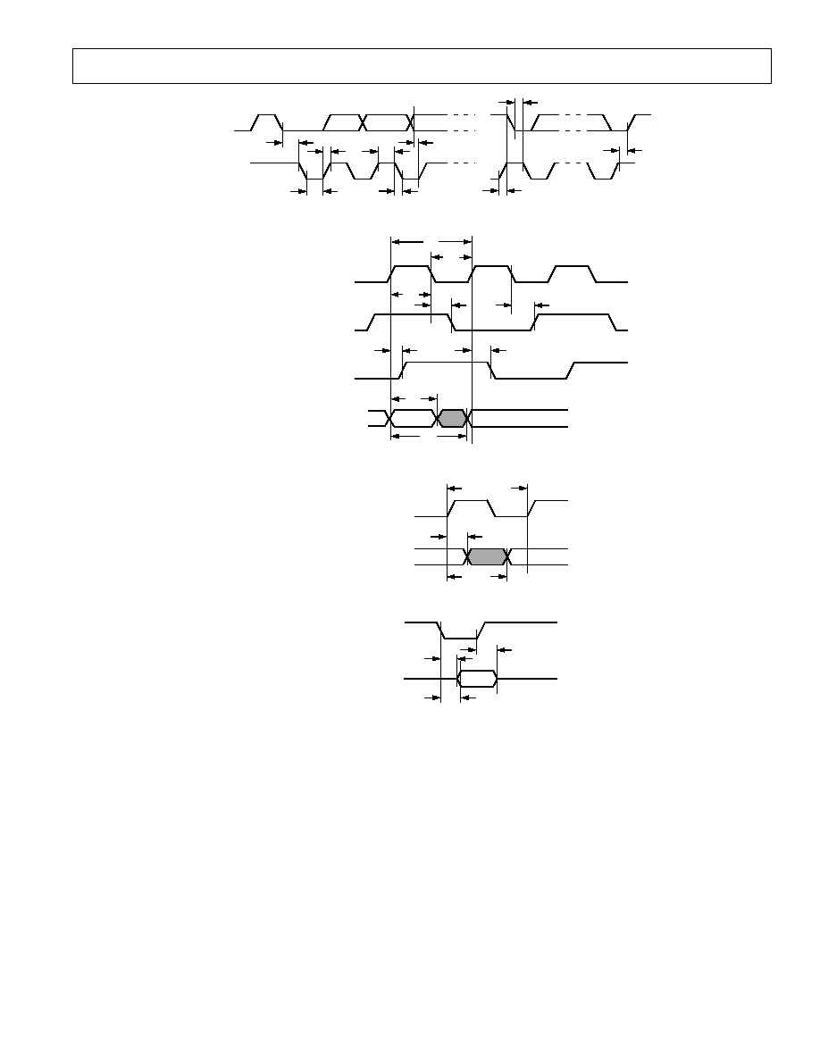
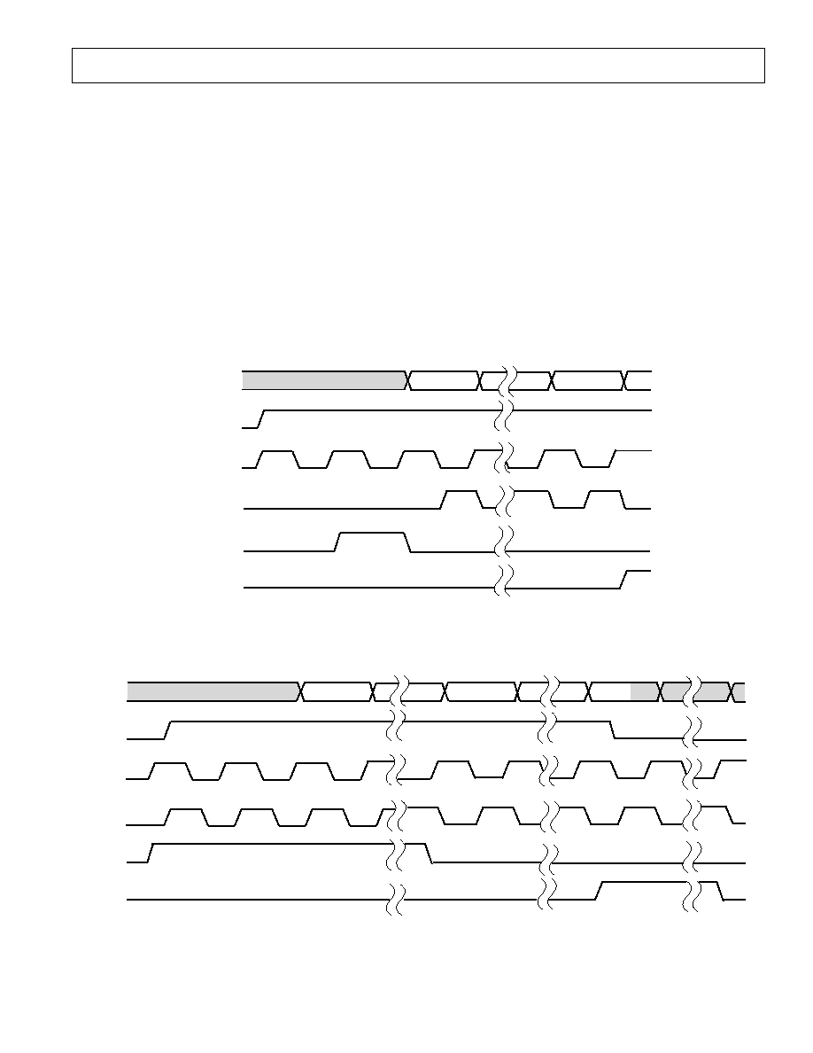
Figure 1. MPU Port Timing Diagram
LLC1
LLCREF
LLC2
OUTPUTS P0P19, HREF, VREF,
VSYNC, HSYNC, FIELD, DV
t
12
t
14
t
11
t
10
t
9
t
15
t
16
t
17
t
13
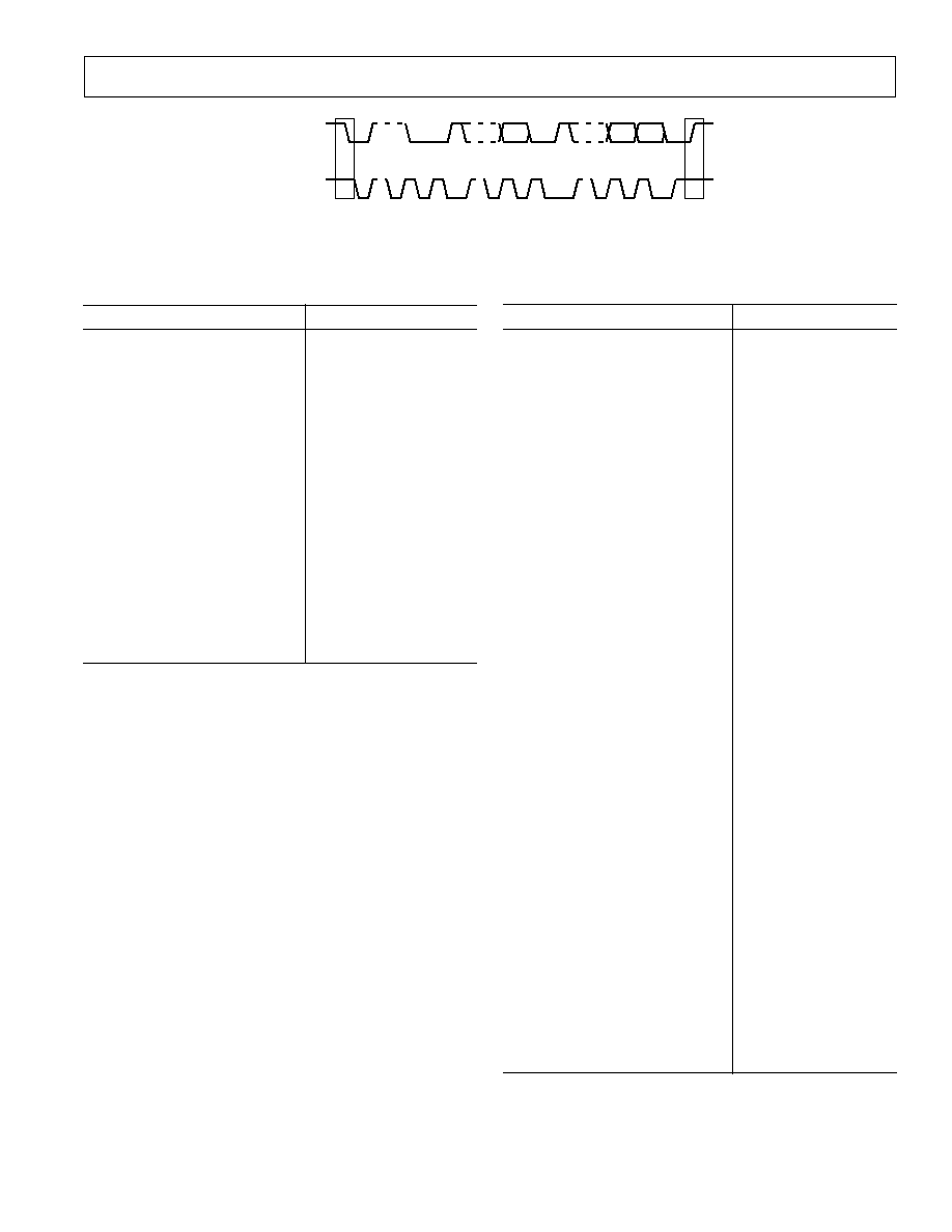
Figure 2. LLC Clock, Pixel Port, and Control Outputs Timing Diagram
CLKIN
OUTPUTS P0P15, HREF, VREF,
VSYNC, HSYNC, FIELD, DV
t
18
t
19
t
20
Figure 3. Pixel Port and Control Outputs in CAPI and SCAPI Mode Timing Diagram
OE
OUTPUTS P0P15, HS,
VS, VREF, HREF, FIELD, DV
t
23
t
21
t
22
Figure 4.
OE Timing Diagram
REV. 0
6
ADV7183
CAUTION
ESD (electrostatic discharge) sensitive device. Electrostatic charges as high as 4000 V readily
accumulate on the human body and test equipment and can discharge without detection. Although the
ADV7183 features proprietary ESD protection circuitry, permanent damage may occur on devices
subjected to high energy electrostatic discharges. Therefore, proper ESD precautions are recommended
to avoid performance degradation or loss of functionality.
WARNING!
ESD SENSITIVE DEVICE
ABSOLUTE MAXIMUM RATINGS
1
V
AA
to GND . . . . . . . . . . . . . . . . . . . . . . . . . . . . . . . . . . . 7 V
V
DD
to GND . . . . . . . . . . . . . . . . . . . . . . . . . . . . . . . . . . . 4 V
V
DDIO
to GND . . . . . . . . . . . . . . . . . . . . . . . . . . . . . . . . . . 4 V
Voltage on Digital Input Pins . . GND 0.5 V to V
AA
+ 0.5 V
Storage Temperature (T
S
) . . . . . . . . . . . . . . 65
°C to +150°C
Junction Temperature (T
J
) . . . . . . . . . . . . . . . . . . . . . . 150
°C
Lead Temperature (Soldering, 10 sec) . . . . . . . . . . . . . 260
°C
Analog Outputs to GND
2
. . . . . . . . . . . . GND 0.5 V to V
AA
NOTES
1
Stresses above those listed under Absolute Maximum Ratings may cause perma-
nent damage to the device. This is a stress rating only; functional operation of the
device at these or any other conditions above those listed in the operational sections
of this specification is not implied. Exposure to absolute maximum rating condi-
tions for extended periods may affect device reliability.
2
Analog output short circuit to any power supply or common can be of an indefinite
duration.
ORDERING GUIDE
Model
Temperature Range
Package
ADV7183KST
0
°C to 70°C
80-LQFP
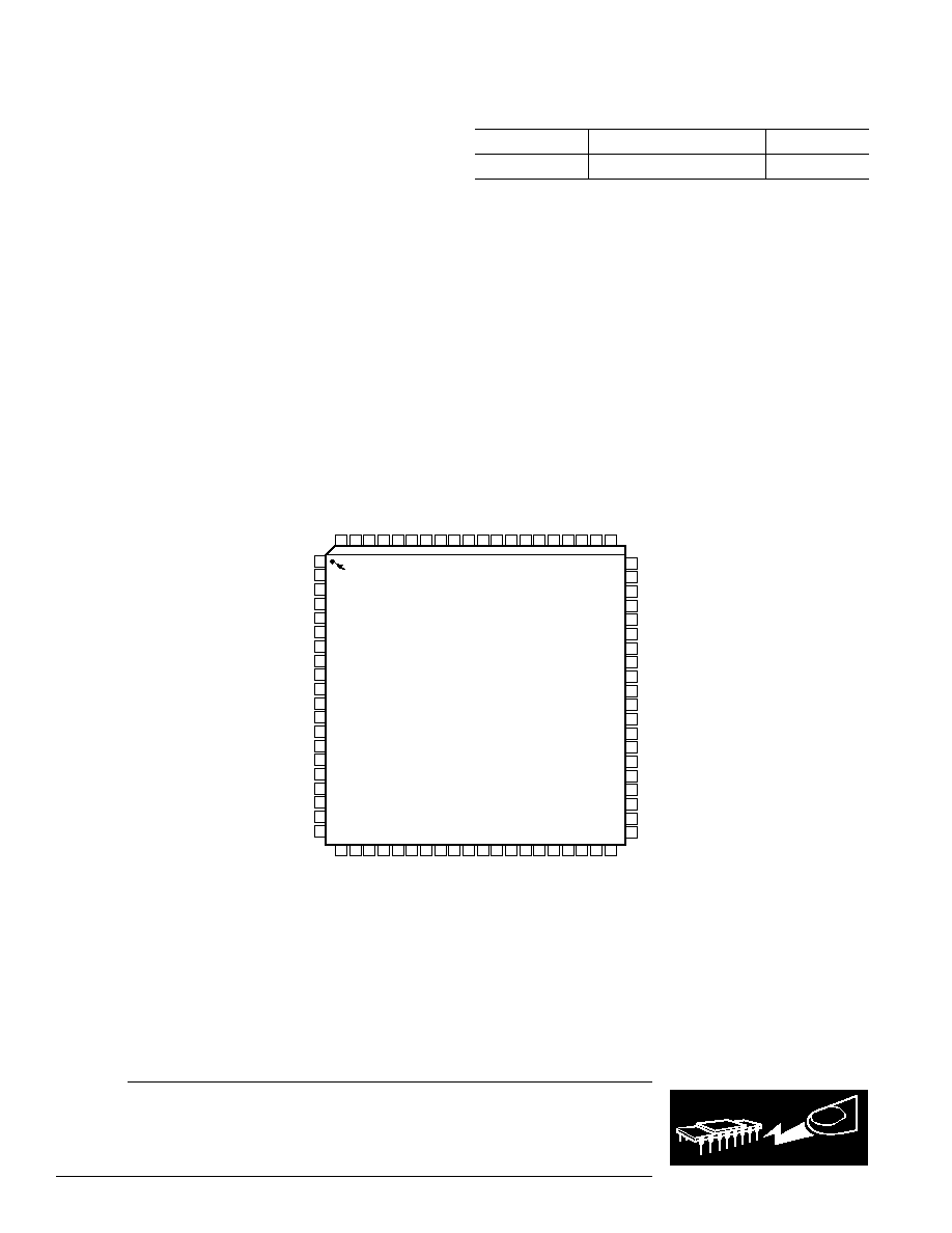
PIN CONFIGURATION
80 79 78 77 76
71 70 69 68 67 66 65
75 74 73 72
64 63 62 61
1
2
3
4
5
6
7
8
9
10
11
13
14
15
16
12
17
18
20
19
21 22 23 24 25 26 27 28 29 30 31 32 33 34 35 36 37 38 39 40
PIN 1
IDENTIFIER
TOP VIEW
(Not to Scale)
60
59
58
57
56
55
54
53
52
51
50
49
48
47
46
45
44
43
42
41
FIELD
OE
DV
RD
P12
P13
P14
P15
D
V
DD3
D
VSS3
HREF/
HRESET
VREF/
VRESET
SCLK
SD
A
T
A
ALSB
ISO
RESET
A
VSS
AIN6
A
VSS6
VS/ACTIVE
HS/ACTIVE
DVSSIO
DVDDIO
P11
P10
P9
P8
DVSS2
DVDD2
AFF
HFF/QCLK/GL
AEF
DVSSIO
DVDDIO
CLKIN
GPO3
GPO2
P7
P6
AIN5
AVSS5
AIN4
AVSS4
AVSS
CAPC2
CAPC1
AVSS
CML
REFOUT
AVDD
CAPY2
CAPY1
AVSS
AIN3
AVSS3
P5
P4
P3
P2
LLCREF
LLC2
LLC1/PCLK
XT
AL1
XT
AL
D
V
DD1
P1
P0
GPO1
GPO0
PWRDN
D
VSS1
AD7183
AIN2
AVSS2
AIN1
AVSS1
ELPF
PVDD
PVSS
A
VSS
REV. 0
ADV7183
7
PIN FUNCTION DESCRIPTIONS
Pin
Mnemonic
Input/Output
Function
1
VS/VACTIVE
O
VS or Vertical Sync. A dual-function pin, (OM_SEL[1:0] = 0, 0) is an
output signal that indicates a vertical sync with respect to the YUV pixel
data. The active period of this signal is six lines of video long. The polarity
of the VS signal is controlled by the PVS bit. VACTIVE (OM_SEL[1:0] =
1, 0 or 0, 1) is an output signal that is active during the active/viewable
period of a video field. The polarity of VACTIVE is controlled by PVS bit.
2
HS/HACTIVE
O
HS or Horizontal Sync. A dual-function pin, (OM_SEL[1:0] = 0, 0) is a
programmable horizontal sync output signal. The rising and falling edges
can be controlled by HSB[9:0] and HSE[9:0] in steps of 2 LLC1. The polarity
of the HS signal is controlled by the PHS bit. HACTIVE (OM_SEL[1:0] =
1, 0 or 0, 1) is an output signal that is active during the active/viewable
period of a video line. The active portion of a video line is programmable on
the ADV7183. The polarity of HACTIVE is controlled by PHS bit.
3, 14
DVSSIO
G
Digital I/O Ground
4, 15
DVDDIO
P
Digital I/O Supply Voltage (3.3 V)
58, 1924,
P15P0
O
Video Pixel Output Port. 8-bit multiplexed YCrCb pixel port (P15P8),
32, 33, 7376
16-bit YCrCb pixel port (P15P8 = Y and P7P0 = Cb,Cr).
9, 31, 71
DVSS13
G
Ground for Digital Supply
10, 30, 72
DVDD13
P
Digital Supply Voltage (3.3 V)
11
AFF
O
Almost Full Flag. A FIFO control signal indicating when the FIFO has
reached the almost full margin set by the user (use FFM[4:0]). The polarity
of this signal is controlled by the PFF bit.
12
HFF/QCLK/GL
I/O
Half Full Flag. A multifunction pin, (OM_SEL[1:0] = 1, 0) is a FIFO
control signal that indicates when the FIFO is half full. The QCLK
(OM_SEL[1:0] = 0, 1) pin function is a qualified pixel output clock when
using FIFO SCAPI mode. The GL (OM_SEL[1:0] = 0, 0) function
(Genlock output) is a signal that contains a serial stream of data that contains
information for locking the subcarrier frequency. The polarity of HFF signal
is controlled by PFF bit.
13
AEF
O
Almost Empty Flag. A FIFO control signal, it indicates when the FIFO
has reached the almost empty margin set by the user (use FFM[4:0]). The
polarity of this signal is controlled by PFF bit.
16
CLKIN
I
Asynchronous FIFO Clock. This asynchronous clock is used to output
data onto the P19-P0 bus and other control signals.
17, 18, 34, 35
GPO[3:0]
O
General-Purpose Outputs controlled via I
2
C
25
LLCREF
O
Clock Reference Output. This is a clock qualifier distributed by the inter-
nal CGC for a data rate of LLC2. The polarity of LLCREF is controlled
by the PLLCREF bit.
26
LLC2
O
Line-Locked Clock System Output Clock/2 (13.5 MHz)
27
LLC1/PCLK
O
Line-Locked Clock System Output Clock. A dual-function pin (27 MHz
± 5%)
or a FIFO output clock ranging from 20 MHz to 35 MHz.
28
XTAL1
O
Second terminal for crystal oscillator; not connected if external clock
source is used.
29
XTAL
I
Input terminal for 27 MHz crystal oscillator or connection for external
oscillator with CMOS-compatible square wave clock signal
36
PWRDN
I
Power-Down Enable. A logical low will place part in a power-down status.
37
ELPF
I
This pin is used for the External Loop Filter that is required for the LLC PLL.
38
PVDD
P
39
PVSS
G

REV. 0
8
ADV7183
PIN FUNCTION DESCRIPTIONS (continued)
Pin
Mnemonic
Input/Output
Function
40, 47, 53, 56,
AVSS
G
Ground for Analog Supply
63
41, 43, 45, 57,
AVSS16
G
Analog Input Channels. Ground if single-ended mode is selected. These
59, 61
pins should be connected directly to REFOUT when differential mode is
selected.
42, 44, 46, 58,
AIN16
I
Video Analog Input Channels
60, 62
48, 49
CAPY12
I
ADC Capacitor Network
50
AVDD
P
Analog Supply Voltage (5 V)
51
REFOUT
O
Internal Voltage Reference Output
52
CML
O
Common-Mode Level for ADC
54, 55
CAPC12
I
ADC Capacitor Network
64
RESET
I/O
System Reset Input. Active Low.
65
ISO
I
Input Switch Over. A low to high transition on this input indicates to the
decoder core that the input video source has been changed externally and
configures the decoder to reacquire the new timing information of the new
source. This is useful in applications where external video muxes are used.
This input gives the advantage of faster locking to the external muxed
video sources. A low to high transition triggers this input.
66
ALSB
I
TTL Address Input. Selects the MPU address:
MPU address = 88h ALSB = 0, disables I
2
C filter
MPU address = 8Ah ALSB = 1, enables I
2
C filter
67
SDATA
I/O
MPU Port Serial Data Input/Output
68
SCLK
I
MPU Port Serial Interface Clock Input
69
VREF/
VRESET
O
VREF or Vertical Reference Output Signal. Indicates start of next field.
VRESET or Vertical Reset Output is a signal that indicates the beginning
of a new field. In SCAPI/CAPI mode this signal is one clock wide and
active low relative to CLKIN. It immediately follows the
HRESET pixel,
and indicates that the next active pixel is the first active pixel of the next
field.
70
HREF/
HRESET
O
HREF or Horizontal Reference Output Signal. A dual-function pin
(enabled when Line-Locked Interface is selected, OM_SEL[1:0] = 0,0),
this signal is used to indicate data on the YUV output. The positive slope
indicates the beginning of a new active line; HREF is always 720 Y samples
long.
HRESET or Horizontal Reset Output (enabled when SCAPI or
CAPI is selected, OM_SEL[1:0] = 0, 1 or 1, 0) is a signal that indicates the
beginning of a new line of video. In SCAPI/CAPI this signal is one clock
cycle wide and is output relative to CLKIN. It immediately follows the last
active pixel of a line. The polarity is controlled via PHVR.
77
RD
I
Asynchronous FIFO Read Enable Signal. A logical high on this pin enables
a read from the output of the FIFO.
78
DV
O
DV or Data Valid Output Signal. In SCAPI/CAPI mode, DV performs two
functions, depending on whether SCAPI or CAPI is selected. It toggles
high when the FIFO has reached the AFF margin set by the user, and
remains high until the FIFO is empty. The alternative mode is where it can
be used to control FIFO reads for bursting information out of the FIFO. In
API mode DV indicates valid data in the FIFO, which includes both pixel
information and control codes. The polarity of this pin is controlled via PDV.
79
OE
I
Output Enable Controls Pixel Port Outputs. A logic high will three-state
P19P0.
80
FIELD
O
ODD/EVEN Field Output Signal. An active state indicates that an even
field is being digitized. The polarity of this signal is controlled by the PF bit.
REV. 0
ADV7183
9
(FEATURES continued from page 1)
CCIR/Square Pixel Operation
Integrated On-Chip Video Timing Generator
Synchronous or Asynchronous Output Timing
Line-Locked Clock Output
Closed Captioning Passthrough Operation
Vertical Blanking Interval Support
Power-Down Mode
2-Wire Serial MPU Interface (I
2
C-Compatible)
5 V Analog 3.3 V Digital Supply Operation
80-Lead LQFP Package
GENERAL DESCRIPTION
The ADV7183 is an integrated video decoder that automatically
detects and converts a standard analog baseband television sig-
nal compatible with worldwide standards NTSC or PAL into
4:2:2 or 4:1:1 component video data compatible with 16-/8-bit
CCIR601/CCIR656.
The advanced and highly flexible digital output interface
enables performance video decoding and conversion in both
frame-buffer-based and line-locked clock-based systems. This
makes the device ideally suited for a broad range of applica-
tions with diverse analog video characteristics, including
tape-based sources, broadcast sources, security/surveillance
cameras, and professional systems.
Fully integrated line stores enable real-time horizontal and
vertical scaling of captured video down to icon size. The 10-bit
accurate A/D conversion provides professional quality SNR
performance. This allows true 8-bit resolution in the 8-bit out-
put mode.
The six analog input channels accept standard composite,
S-video, and component YCrCb video signals in an extensive
number of combinations. AGC and clamp restore circuitry
allow an input video signal peak-to-peak range of 0.5 V up to
2 V. Alternatively, these can be bypassed for manual settings.
The fixed 27 MHz clocking of the ADCs and data path for all
modes allows very precise and accurate sampling and digital
filtering. The line-locked clock output allows the output data
rate, timing signals, and output clock signals to be synchronous,
asynchronous, or line-locked even with
±5% line length varia-
tion. The output control signals allow glueless interface
connection in almost any application.
The ADV7183 modes are set up over a 2-wire serial bidirec-
tional port (I
2
C-compatible).
The ADV7183 is fabricated in a 5 V CMOS process. Its mono-
lithic CMOS construction ensures greater functionality with
lower power dissipation.
The ADV7183 is packaged in a small 80-pin LQFP package.
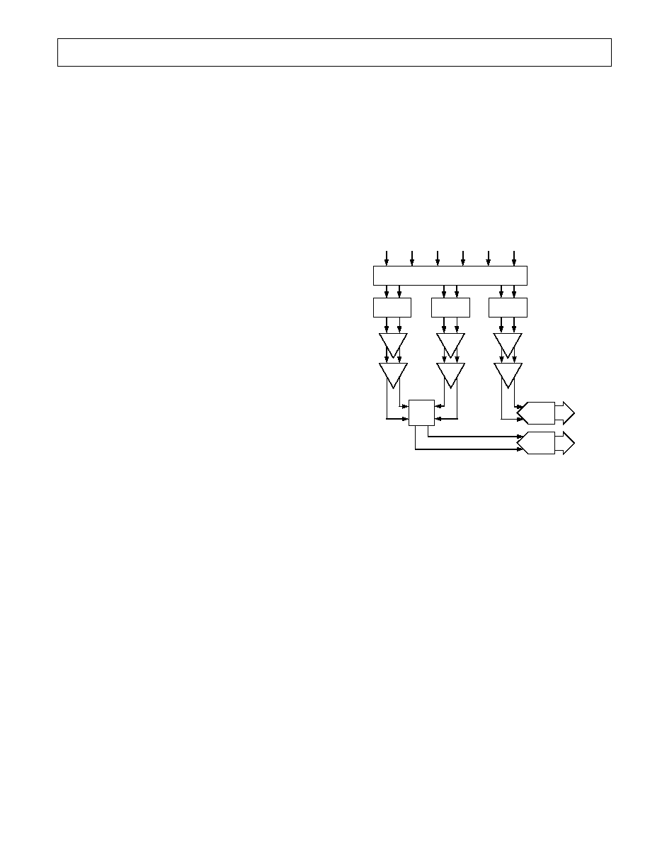
ANALOG INPUT PROCESSING
The ADV7183 has six analog video input channels. These six
channels can be arranged in a variety of configurations to support
up to six CVBS input signals, three S-video input signals, and two
YCrCb component analog video input signals. The INSEL[3:0]
bits control the input type and channel selected. The analog
front end includes three clamp circuits for DC restore. There are
three sample-and-hold amplifiers prior to the ADC which are
used to enable simultaneous sampling of up to three channels in
a YCrCb input mode. Two 10-bit ADCs are used for sampling.
The entire analog front end is fully differential which ensures that
the video is captured to the highest quality possible. This is very
important in highly integrated systems such as video decoders.
Figure 5 shows the analog front end section of the ADV7183.
CLAMP V
1
CLAMP U
1
MUX 6CVBS 3YC 2YUV
SHA
2
SHA
2
SHA
2
MUX
Y ADC
2
C ADC
2
NOTES
ANALOG SIGNAL PATH KEPT FULLY DIFFERENTIAL
ADCs: 10-BIT ACCURATE; 12dB GAIN RANGE
1
CLAMP BLOCKS CONTAIN A SET OF CURRENT SOURCES FOR DC
RESTORATION; U AND V HAVE ONLY HALF BANDWIDTH (SAMPLED
SIMULTANEOUSLY, CONVERTED SEQUENTIALLY)
2
PIPELINED
10
10
CLAMP Y
1
Figure 5. Analog Front End Block Diagram
CLAMPING
The clamp control on the ADV7183 consists of a digitally
controlled analog current and voltage clamp and a digitally
controlled digital clamp circuit. The coupling capacitor on each
channel is used to store and filter the clamping voltage. A digital
controller controls the clamp up and down current sources that
charge the capacitor on every line. Four current sources are
used in the current clamp control, two large current sources are
used for coarse clamping, and two small current sources are used
for fine clamping. The voltage clamp, if enabled, is only used on
startup or if a channel is switched. This clamp pulls the video
into the midrange of the ADC, which results in faster clamping
and faster lock-in time for the decoder. The fourth clamp con-
troller is fully digital and clamps the ADC output data, which
results in extremely accurate clamping. It also has the added
advantage of being fully digital, which results in very fast clamp
timing and makes the entire clamping process very robust in
terms of handling large amounts of hum that can be present on
real-world video signals.
REV. 0
10
ADV7183
In S-video mode there are two clamp controllers used to sepa-
rately control the luminance clamping and the chrominance
clamping. Also in YCrCb component input mode there are two
clamp controllers used to control the luminance clamping and
the CrCb clamping separately; there are, however, individual
current clamps on the Cr and Cb inputs.
User programmability is built into the clamp controllers which
enable the current and digital clamp controllers to be set up to
user-defined conditions. Refer to analog clamp control register
(14H), digital clamp control register (15H), and digital color
clamp offset register (15H and 16H) for control settings.
ANALOG-TO-DIGITAL CONVERTERS
Two 10-bit ADCs are used in the ADV7183, and they run from
a 27 MHz input clock. An integrated band gap generates the
required reference voltages for the converters. If the decoder is
configured in CVBS mode, the second ADC can be switched off
to reduce power consumption, see PSC[1:0].
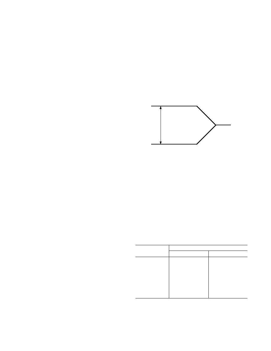
AUTOMATIC GAIN CONTROL
The AGC control block on the ADV7183 is a digitally based
system. This controller ensures that the input video signal
(CVBS, S-video, or YCrCb) is scaled to its correct value such
that the YCrCb digital output data matches the correct gain of
the video signal. The AGC has an analog input video range of
0.5 V p-p to 2.0 V p-p, which gives a 6 dB to +6 dB gain range.
Figure 6 demonstrates this range. This AGC range will compensate
for video signals that have been incorrectly terminated or have
been attenuated due to cable loss or other factors.
There are two main control blocks: one for the luminance chan-
nel and one for the chrominance channel.
The luminance automatic gain control has eight modes of
operation:
1. Manual AGC mode where gain for the luminance path is set
manually using LGM[11:0].
2. Blank level to sync tip is used to set the luminance gain;
manual MIRE[2:0] controls the maximum value through the
luminance channel. There is no override of this mode when
white peak mode is detected.
3. Blank level to sync tip is used to set luminance gain; manual
MIRE[2:0] controls the maximum value through luminance
channel. There is override of this mode when white peak
mode is detected. White peak mode is activated when the
input video exceeds the maximum luminance range for long
periods; this mode is designed to prevent clipping of the
input video signal.
4. Blank level to sync tip is used to set luminance gain;
MIRE[2:0] is automatically controlled to set the maximum
value through the luminance channel. There is no override
of this mode when white peak mode is detected.
5. Blank level to sync tip is used to set luminance gain; manual
MIRE[2:0] is automatically controlled to set the maximum
value through the luminance channel. There is override of
this mode when white peak mode is detected. White peak
mode is activated when the input video exceeds the maxi-
mum luminance range for long periods; this mode is designed
to prevent clipping of the input video signal.
6. Based on active video peak white. PW_UPD sets the gain
update frequency (once per field).
7. Based on average active video. PW_RES sets what lines are used;
only relevant if the signal conforms to PAL 625 line standard.
8. The luminance channel gain is frozen at its present value.
6
ANALOG INPUT LEVEL 2V p-p
dB
0
6
CONTR
O
LLED ADC INPUT LEVEL
dB
0
RANGE = 12dB
MAXIMUM
MINIMUM
Figure 6. Analog Input Range
The chrominance automatic gain control has four modes of
operation:
1. Manual AGC mode where gain for chrominance path is set
manually using CGM[11:0].
2. Luminance gain used for chrominance channel.
3. Chrominance automatic gain based on color burst amplitude.
4. Chrominance gain frozen at its present setting.
Both the luminance and chrominance AGC controllers have a
programmable time constant that allows the AGC to operate in
four modes: slow, medium, fast, and video quality controlled.
The maximum IRE (MIRE[2:0]) control can be used to set the
maximum input video range that can be decoded. Table I shows
the selectable range.
Table I. MIRE Control
Function
MIRE[2:0]
PAL (IRE)
NTSC (IRE)
0
0
0
133
122
0
0
1
125
115
0
1
0
120
110
0
1
1
115
105
1
0
0
110
100
1
0
1
105
100
1
1
0
100
100
1
1
1
100
100
REV. 0
ADV7183
11
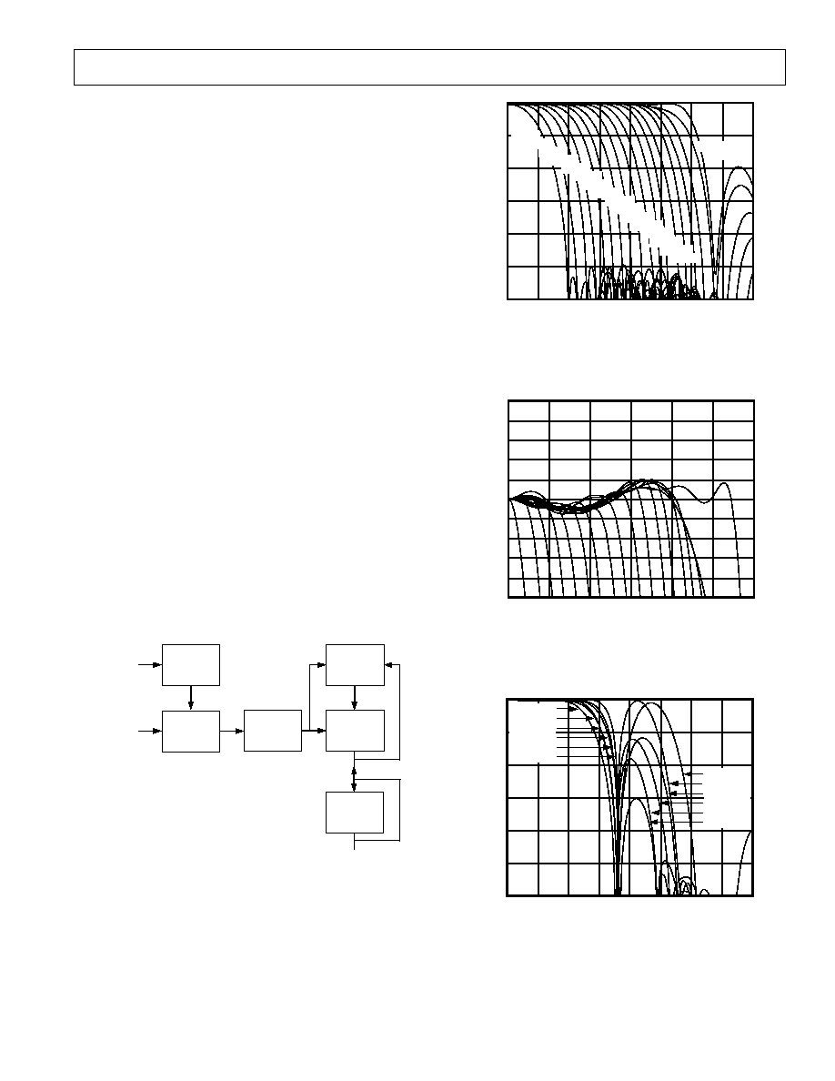
LUMINANCE PROCESSING
Figure 7 shows the luminance data path. The 10-bit data from
the Y ADC is applied to an antialiasing low pass filter that is
designed to band-limit the input video signal such that aliasing
does not occur. This filter dramatically reduces the design on an
external analog antialaising filter; this filter need only remove
components in the input video signal above 22 MHz. The data
then passes through a shaping or notch filter.
When in CVBS mode a notch filter must be used to remove the
unwanted chrominance data that lies around the subcarrier
frequency. A wide variety of programmable notch filters for
both PAL and NTSC are available. The YSFM[4:0] control the
selection of these filters; refer to Figures 8 to 16 for plots of
these filters. If S-video or component mode is selected a notch
filter is not required. The ADV7183 offers 18 possible shaping
filters (SVHS1-18) with a range of low pass filter responses from
0.5 MHz up to 5.75 MHz. The YSFM[4:0] control the selec-
tion of these filters. Please refer to Figures 8 through 16 for
filter plots.
The next stage in the luminance processing path is a peaking
filter; this filter offers a sharpness function on the luminance
path. The degree of sharpness can be selected using YPM[2:0].
If no sharpness is required, this filter can be bypassed.
The luminance data is then passed through a resampler to correct
for line length variations in the input video. This resampler is
designed to always output 720 pixels per line for standard PAL or
NTSC. The resampler used on the ADV7183 is of very high
quality as it uses 128 phases to resample the video, giving 1/128
pixel resolution. The resampler is controlled by a sync detection
block that calculates line length variations on the input video.
The final stage in the luminance path, before it is applied to an
output formatter block, is a two-line delay store that is used to
compensate for delays in the chroma data path when chroma
comb filter is selected.
ANTI-
ALIASING
LPF
SHAPING
AND
NOTCH
FILTER
PEAKING
FILTER
RESAMPLE
DELAY
LINE
STORES
SYNC
DETECTION
Y
ADC DATA
Figure 7. Luminance Processing Path
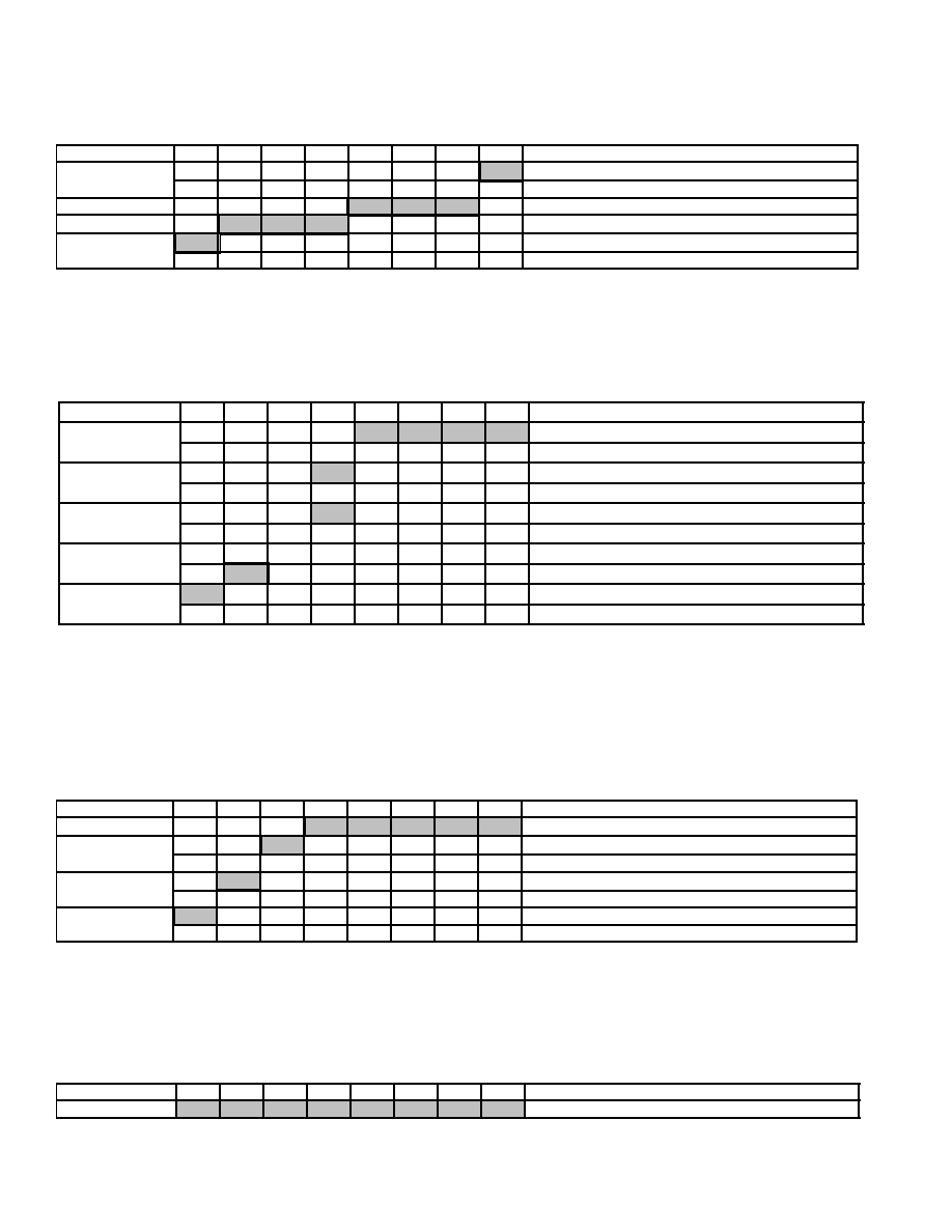
FREQUENCY MHz
0
60
0
8
1
A
T
TENU
A
T
ION
dB
2
3
4
5
6
7
10
20
30
40
50
SVHS1
SVHS2
SVHS3
SVHS4
SVHS5
SVHS6
SVHS7
SVHS8
SVHS9
SVHS10
SVHS11
SVHS12
SVHS13
SVHS14
SVHS15
SVHS16
SVHS17
SVHS18
Figure 8. Luminance SVHS118 Shaping Filter
Responses
FREQUENCY MHz
1.0
1.0
0
6
1
A
T
TENU
A
T
ION
dB
2
3
4
5
0.8
0.2
0.4
0.6
0.8
0.6
0.4
0
0.2
Figure 9. Luminance SVHS1SVHS18 Shaping
Filter Responses (Close-Up)
FREQUENCY MHz
0
60
0
8
1
A
T
TENU
A
T
ION
dB
2
3
4
5
6
7
10
20
30
40
50
NTSC WN1
NTSC WN2
NTSC WN3
NTSC NN1
NTSC NN2
NTSC NN3
NTSC WN2
NTSC NN3
NTSC WN1
NTSC NN2
NTSC NN1
NTSC WN3
Figure 10. Luminance NTSC Narrow/Wide Notch
Shaping Filter
REV. 0
12
ADV7183
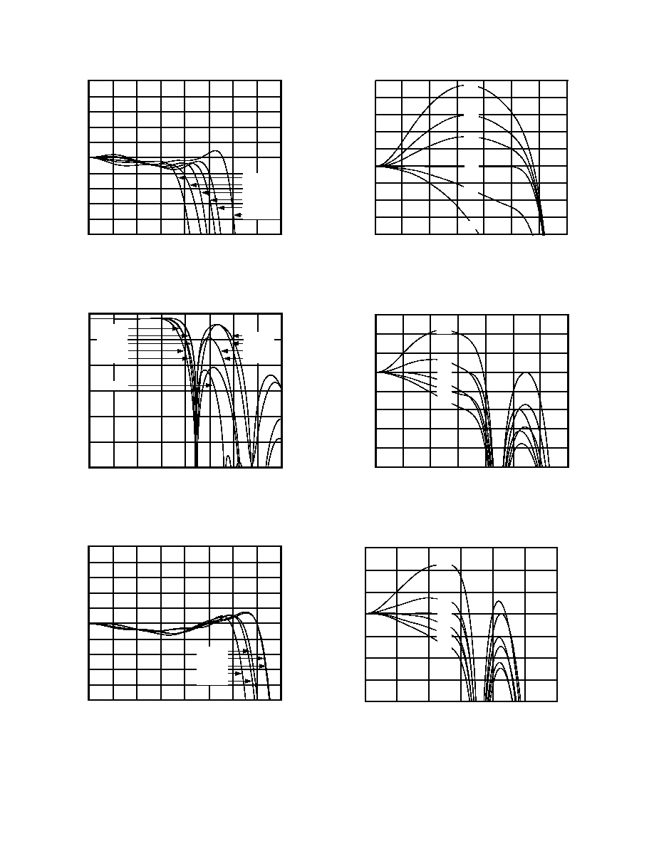
FREQUENCY MHz
1.0
1.0
0
4.0
0.5
A
T
TENU
A
T
ION
dB
1.0
1.5
2.0
2.5
3.0
3.5
0.8
0.4
0.2
0.6
0.8
0.6
0.2
0
0.4
NTSC WN1
NTSC WN2
NTSC WN3
NTSC NN1
NTSC NN2
NTSC NN3
Figure 11. Luminance NTSC Narrow/Wide Notch
Shaping Filter (Close-Up)
FREQUENCY MHz
0
60
0
8
1
A
T
TENU
A
T
ION
dB
2
3
4
5
6
7
10
20
30
40
50
PAL NN1
PAL NN2
PAL NN3
PAL W1
PAL W2
PAL NN3
PAL W1
PAL W2
PAL NN2
PAL NN1
Figure 12. Luminance PAL Narrow/Wide Notch
Shaping Filter Responses
FREQUENCY MHz
1.0
1.0
0
4.0
0.5
A
T
TENU
A
T
ION
dB
1.0
1.5
2.0
2.5
3.0
3.5
0.8
0.4
0.2
0.6
0.8
0.6
0.2
0
0.4
PAL NN1
PAL NN2
PAL NN3
PAL WN1
PAL WN2
Figure 13. Luminance PAL Narrow/Wide Notch
Shaping Filter Responses (Close-Up)
FREQUENCY MHz
0
1
2
3
4
5
6
7
10
8
8
A
T
TENU
A
T
ION
dB
0
2
4
6
4
2
6
PS1
PS4
PS3
PS2
PS5
PS6
Figure 14. Luminance Peaking Filter Responses in
S-Video (SVHS17 Selected)
FREQUENCY MHz
0
7
1
2
3
4
5
6
6
10
A
TTENU
A
TION
dB
4
2
4
6
8
2
0
PC1
PC4
PC3
PC2
PC5
PC6
Figure 15. Luminance Peaking Filter Responses in
CVBS (PAL NN3 Selected)
FREQUENCY MHz
6
8
0
6
1
A
T
TENU
A
T
ION
dB
2
3
4
5
4
2
0
4
6
2
PC1
PC4
PC3
PC2
PC5
PC6
Figure 16. Luminance Peaking Filter Responses in
CVBS (NTSC NN3 Selected)
REV. 0
ADV7183
13
CHROMINANCE PROCESSING
Figure 17 shows the chrominance data path. The 10-bit data
from the Y ADC (CVBS mode) or the C ADC (S-video) is first
demodulated. The demodulation is achieved by multiplying by
the locally generated quadrature subcarrier, where the sign of
the cos subcarrier is inverted from line to line according to the
PAL switch, and then low pass filtering is applied to removed
components at twice the subcarrier frequency. For NTSC, the
phase of the locally generated subcarrier during color burst is
the same as the phase of the color burst. For PAL, the phase of
the color burst changes from line to line, relative to the phase
during active video, and the phase of the locally generated
subcarrier is the average of these two values.
The chrominance data is then passed through an antialiasing
filter which is a band-pass filter to remove the unwanted lumi-
nance data. This antialaising filter dramatically reduces the
external antialaising filter requirements as it has only to filter
components above 25 MHz. In component mode the demodu-
lation block is bypassed.
The next stage of processing is a shaping filter that can be used
to limit the chrominance bandwidth to between 0.5 MHz
and 3 MHz; the CSFM[2:0] can be used to select these
responses. It should be noted that in CVBS mode a filter of no
greater than 1.5 MHz should be selected, as CVBS video is
typically band-limited to below 1.5 MHz. In S-video mode a
filter of up to 2 MHz can be used. In component mode a filter
of up to 3 MHz can be used as component video has higher
bandwidth than CVBS or S-video.
The chrominance data is then passed through a resampler to
correct for line length variations in the input video. This
resampler is designed to always output 720 pixels per line for
standard PAL or NTSC. The resampler used on the ADV7183
is of very high quality as it uses 64 phases to resample the video,
giving 1/64 pixel resolution. The resampler is controlled by a
sync detection block that calculates line length variations on the
input video.
The final stage in the chrominance path, before it is applied to
an output formatter block, is chroma comb filter.
ANTI-
ALIASING
LPF
SHAPING
LPF
RESAMPLE
CHROMA
COMB
FILTERS
SYNC
DETECTION
U/V
CV/C
27MHz
SINE
ANTI-
ALIASING
LPF
COSINE
13.5MHz
13.5MHz
6.75MHz
SUBCARRIER
RECOVERY
INTERLEAVE
Figure 17. Chrominance Processing Path
FREQUENCY MHz
0
60
0
4.0
0.5
A
T
TENU
A
T
ION
dB
1.0
1.5
2.0
2.5
3.0
3.5
10
20
30
40
50
SH2 SH3 SH4 SH5
SH6
SH1
Figure 18. Chrominance Shaping Filter Responses
FREQUENCY MHz
1.0
1.0
0
4.0
0.5
A
T
TENU
A
T
ION
dB
1.0
1.5
2.0
2.5
3.0
3.5
0.8
0.4
0.2
0.6
0.8
0.6
0.2
0
0.4
SH2 SH3 SH4 SH5
SH1
SH6
Figure 19. Chrominance Shaping Filter Responses
(Close-Up)
REV. 0
14
ADV7183
OUTPUT INTERFACE
Mode Selection Overview
The ADV7183 supports three output interfaces: LLC-compatible
synchronous pixel interface, the CAPI interface, and the SCAPI
interface. When the part is configured in the synchronous pixel
interface mode, pixel and control data are output synchronous with
LLC1 (8-bit mode) or LLC2 (16-bit mode). In this mode control
and timing information for field, vertical blanking, and horizontal
blanking identification may also be encoded as control codes.
When configured in CAPI or SCAPI mode only the active
pixel data is output synchronous with the CLKIN (asynchronous
FIFO clock). The pixels are output via a 512-pixel deep, 20-bit
wide FIFO. HACTIVE and VACTIVE are output on independent
pins. HACTIVE will be active during the active viewable period
of a video line and VACTIVE will be active during the active
viewable period of a video field. CAPI and SCAPI modes will
always output data in 16-bit, so this mode of operation cannot be
used when an 8-bit or 10-bit output interface is required. After
power-up, the ADV7183 will default to the LLC-compatible
8-bit CCIR656 4:2:2 @ LLC.
Synchronous Pixel Interface
When the output is configured for an 8-bit pixel interface, the
data is output on the pixel output port P[15:8]. In this mode,
8 bits of chrominance data will precede 8 bits of luminance
data. New pixel data is output on the pixel port after each
rising edge of LLC1. When the output is configured for a 16-
bit pixel interface, the luminance data is output on P[15:8]
and the chrominance data on P[7:0]. In this mode the data is
output with respect to LLC2. Figure 20 shows the basic timing
relationship for this mode.
PIXEL DATA
SAV
P15-8[7:0]
LLC1
LLC2
PIXEL DATA
P7-0[7:0]
SAV
SAV
SAV
Y0
Y1
Y2
Y3
Y4
Cb0
Cr0
Cb1
Cr1
Cb2
00
FF
XY
00
Figure 20. Synchronous Pixel Interface, 16-Bit Example
REV. 0
ADV7183
15
HREF
DV
VREF
VSYNC
FIELD
SAV/EAV V BIT
SAV/EAV H BIT
SAV/EAV F BIT
CVBS INPUT
Figure 21. NTSC End Even Field (LLC Mode)
HREF
DV
VREF
VSYNC
FIELD
SAV/EAV V BIT
SAV/EAV H BIT
SAV/EAV F BIT
CVBS INPUT
Figure 22. NTSC End Odd Field (LLC Mode)
REV. 0
16
ADV7183
HREF
DV
VREF
VSYNC
FIELD
SAV/EAV V BIT
SAV/EAV H BIT
SAV/EAV F BIT
CVBS INPUT
Figure 23. PAL End Even Field (LLC Mode)
HREF
DV
VREF
VSYNC
FIELD
SAV/EAV V BIT
SAV/EAV H BIT
SAV/EAV F BIT
CVBS INPUT
Figure 24. PAL End Odd Field (LLC Mode)
REV. 0
ADV7183
17
Control and Pixel Interface FIFO Modes
When the ADV7183 is configured to operate in this mode, pixel
data generated within the part is buffered by a 512-pixel deep
FIFO. Only active video pixels and control codes are written into
the FIFO; the others have been dropped. In this mode the output
is operating asynchronously and a CLKIN must be provided to
clock pixels out of the FIFO. The CLKIN must operate faster than
the effective data transfer rate into the FIFO. This rate will be
determined by the number of active pixels per line. If the CLKIN
is not above this, the FIFO may overflow. The ADV7183 controls
the FIFO when set to operate in SCAPI mode. DV (data valid) is
internally fed back to the RD (read enable), unlike the synchronous
pixel mode where DV will not indicate the validity of the current
pixel and only acts as an indication of how much data is stored in
the FIFO. DV will go high at the same time as AFF and remain
high until the FIFO is empty.
By internally setting DV to RD the system ensures that the FIFO
never overflows. When using this mode the status of data on the
pixel outputs can be determined by two indicators, DV and QCLK.
DV will go active two clock cycles (LLC1) before valid data appears
on the bus. QCLK is a qualified clock derived from CLKIN, but
will only be present when valid pixel data is output from the FIFO.
DV indicates valid pixel or control code data. Using these two
control signals, the user can differentiate between pixel information
and invalid data. Figure 25 shows the basic timing relationship
for this mode.
The operation of the ADV7183 in CAPI mode is similar to that
of SCAPI mode with the exception that now the FIFO is con-
trolled by the system; the system must monitor the almost full
flag (AFF), the almost empty flag (AEF), and control the FIFO
read enable (RD). Unlike SCAPI mode, the QCLK is not gated
and is therefore continuous. Figure 26 shows the basic timing
relationship of this mode.
PIXEL DATA
DV
CLKIN
QCLK
AFF
AEF
NOTE
THE POLARITY OF AFF AND AEF ARE CONTROLLED BY THE PFF BIT.
DV POLARITY IS SET BY THE PDV BIT.
Figure 25. SCAPI Output Mode FIFO Operation
RD
CLKIN
QCLK
AFF
AEF
NOTE
THE POLARITY OF AFF AND AEF ARE CONTROLLED BY THE PFF BIT.
DATA
Figure 26. CAPI Output Mode FIFO Operation

REV. 0
18
ADV7183
Manual Clock Control
The ADV7183 offers several output clock mode options; the
output clock frequency can be set by the input video line length, a
fixed 27 MHz output, or by a user-programmable value. Informa-
tion on the clock control register at 28h can be found in the
register access map. When Bit 6 of this register (CLKMANE) is
set to Logic "1," the output clock frequency will be determined
by the user-programmable value (CLKVAL[15:0]). Using this
mode the output clock frequency is calculated as:
LLC
CLKVAL
MHz
=
×
×
×
[
: ]
17 0
2
28
3
16
27
20
For example, a required clock frequency of 25 MHz would yield
a CLKVAL of 2D266h (184934).
Color Subcarrier Control
The color subcarrier manual frequency control register
(CSMF[27:0]) can be used to set the DDFS block to a user-
defined frequency. This function can be useful if the color
subcarrier frequency of the incoming video signal is outside the
standard F
SC
lock range. Setting Bit 4 Reg 23h (CSM) to a
Logic "1" enables the manual frequency control, the frequency
of which will be determined by CSMF[27:0]. The value of
CSMF[27:0] can be calculated as:
CSMF
F
MHz
SC
[
: ]
27 0
2
27
28
=
×
*Required
MPU PORT DESCRIPTION
The ADV7183 supports a 2-wire serial (I
2
C-compatible) micro-
processor bus driving multiple peripherals. Two inputs, serial
data (SDATA) and serial clock (SCLOCK) carry information
between any device connected to the bus. Each slave device is
recognized by a unique address. The ADV7183 has two possible
slave addresses for both read and write operations. These are
unique addresses for the device and are illustrated in Figure 27.
The LSB sets either a read or write operation. Logic Level "1"
corresponds to a read operation while Logic Level "0" corre-
sponds to a write operation. A1 is set by setting the ALSB pin of
the ADV7183 to Logic Level "0" or Logic Level "1."
1
0
0
0
1
0
1
A
1
X
2
1
Address Control. Set up by ALSB.
2
Read/Write Control. Write = 0; Read = 1
Figure 27. Slave Address
To control the device on the bus the following protocol must be
followed. First the master initiates a data transfer by establishing
a start condition, defined by a high to low transition on SDATA
while SCLOCK remains high. This indicates that an address/data
stream will follow. All peripherals respond to the start condition
and shift the next 8 bits (7-bit address + R/
W bit). The bits are
transferred from MSB down to LSB. The peripheral that recognizes
the transmitted address responds by pulling the data line low
during the ninth clock pulse. This is known as an acknowledge bit.
All other devices withdraw from the bus at this point and maintain
an idle condition. The idle condition is where the device monitors
the SDATA and SCLOCK lines waiting for the start condition
and the correct transmitted address. The R/
W bit determines the
direction of the data. A Logic "0" on the LSB of the first byte
means that the master will write information to the peripheral.
A Logic "1" on the LSB of the first byte means that the master
will read information from the peripheral.
The ADV7183 acts as a standard slave device on the bus. The
data on the SDATA pin is 8 bits long, supporting the 7-bit
addresses plus the R/
W bit. The ADV7183 has 71 subaddresses
to enable access to the internal registers. It therefore interprets
the first byte as the device address and the second byte as the
starting subaddress. The subaddresses autoincrement, allowing
data to be written to or read from the starting subaddress. A
data transfer is always terminated by a stop condition. The user
can also access any unique subaddress register on a one-by-one
basis, without having to update all the registers.
Stop and start conditions can be detected at any stage during the
data transfer. If these conditions are asserted out of sequence
with normal read and write operations, they cause an immediate
jump to the idle condition. During a given SCLOCK high period
the user should only issue one start condition, one stop condition,
or a single stop condition followed by a single start condition. If
an invalid subaddress is issued by the user, the ADV7183 will
not issue an acknowledge and will return to the idle condition.
If the user exceeds the highest subaddress in autoincrement mode,
the following action will be taken:
1. In read mode, the highest subaddress register contents
will continue to be output until the master device issues a
no-acknowledge. This indicates the end of a read. A
no-acknowledge condition is where the SDATA line is not
pulled low on the ninth pulse.
2. In write mode, the data for the invalid byte will not be loaded
into any subaddress register, a no-acknowledge will be issued
by the ADV7183, and the part will return to the idle condition.
WRITE
SEQUENCE
READ
SEQUENCE
S
SLAVE ADDR
A(S)
DATA
S
A(S)
SLAVE ADDR
SUB ADDR
SUB ADDR
A(S)
A(S)
S
A(S)
SLAVE ADDR
A(S)
DATA
A(M)
· · ·
· · ·
DATA
A(S)
P
DATA
A(M)
P
LSB = 0
LSB = 1
S = START BIT
P = STOP BIT
A(S) = ACKNOWLEDGE BY SLAVE
A(M) = ACKNOWLEDGE BY MASTER
A(S) = NO-ACKNOWLEDGE BY SLAVE
A(M) = NO-ACKNOWLEDGE BY MASTER
Figure 28. Write and Read Sequences
REV. 0
ADV7183
19
REGISTER ACCESSES
The MPU can write to or read from all of the registers of the
ADV7183 except the subaddress register, which is a write only
register. The subaddress register determines which register the
next read or write operation accesses. All communications with
the part through the bus start with an access to the subaddress
register. Then a read/write operation is performed from/to the
target address which then increments to the next address until a
stop command on the bus is performed.
REGISTER PROGRAMMING
The following section describes each register in terms of its
configuration.
Subaddress Register (SR7SR0)
The communications register is an 8-bit write only register. After the
part has been accessed over the bus and a read/write operation is
selected, the subaddress is set up. The subaddress register
determines to/from which register the operation takes place.
Table II shows the various operations under the control of the
subaddress register. Zero should always be written to SR7SR6.
Register Select (SR5SR0)
These bits are set up to point to the required starting address.
Register Name
Addr (Hex)
BASIC BLOCK
Input Control
00
Video Selection
01
Video Enhancement Control
02
Output Control
03
Extended Output Control
04
General-Purpose Output
05
Reserved
06
FIFO Control
07
Contrast Control
08
Saturation Control
09
Brightness Control
0A
Hue Control
0B
Default Value Y
0C
Default Value C
0D
Temporal Decimation
0E
Power Management
0F
Status Register
10
Info Register
11
Register Name
Addr (Hex)
ADVANCED BLOCK
Reserved
12
Analog Control (Internal)
13
Analog Clamp Control
14
Digital Clamp Control 1
15
Digital Clamp Control 2
16
Shaping Filter Control
17
Reserved
18
Comb Filter Control
19
Reserved
1A
Reserved
1B
Reserved
1C
Reserved
1D
Reserved
1E
Reserved
1F
Reserved
20
Reserved
21
Reserved
22
Color Subcarrier Control 1
23
Color Subcarrier Control 2
24
Color Subcarrier Control 3
25
Color Subcarrier Control 4
26
Pixel Delay Control
27
Manual Clock Control 1
28
Manual Clock Control 2
29
Manual Clock Control 3
2A
Auto Clock Control
2B
AGC Mode Control
2C
Chroma Gain Control 1
2D
Chroma Gain Control 2
2E
Luma Gain Control 1
2F
Luma Gain Control 2
30
Manual Gain Shadow Control 1
31
Manual Gain Shadow Control 2
32
Misc Gain Control
33
HSync Position Control 1
34
HSync Position Control 2
35
HSync Position Control 3
36
Polarity Control
37
Reserved
44
Reserved
45
Reserved
F1
Reserved
F2
SDATA
SCLOCK
17
8
9
17
8
9
17
8
9
START ADDR R/
W ACK SUB ADDR
ACK
DATA
ACK
STOP
S
P
Figure 29. Bus Data Transfer
Table II. Subaddress Register

REV. 0
20
ADV7183
Table III. Basic Registers
Addr
Register
(Hex)
D7
D6
D5
D4
D3
D2
D1
D0
Input Control
00
VID SEL.3 VID SEL.2 VID SEL.1 VID SEL.0 INSEL.3
INSEL.2
INSEL.1
INSEL.0
Video Selection
01
ASE
BETACAM 4FSC
DIFFIN
SQPE
VID
VID
QUAL.1
QUAL.0
Video Enhancement
02
COR.1
COR.0
YPM.2
YPM.1
YPM.0
Control
Output Control
03
VBI EN
TOD
OF SEL.3
OF SEL.2
OF SEL.1
OF SEL.O OM SEL.1 OMEL.O
Extended Output
04
BT656-4
RANGE
Control
General-Purpose
05
HL_EN
BL_C_VBI GPEH
GPEL
GP0.3
GP0.2
GP0.1
GP0.0
Output
Reserved
06
FIFO Control
07
FFST
AFR
FR
FFM.4
FFM.3
FFM.2
FFM.1
FFM.0
Contrast Control
08
CON.7
CON.6
CON.5
CON.4
CON.3
CON.2
CON.1
CON.0
Saturation Control
09
SAT.7
SAT.6
SAT.5
SAT.4
SAT.3
SAT.2
SAT.1
SAT.0
Brightness Control
0A
BRI.7
BRI.6
BRI.5
BRI.4
BRI.3
BRI.2
BRI.1
BRI.0
Hue Control
0B
HUE.7
HUE.6
HUE.5
HUE.4
HUE.3
HUE.2
HUE.1
HUE.0
Default Value Y
0C
DEF Y.5
DEF Y.4
DEF Y.3
DEF Y.2
DEF Y.1
DEF Y.0
DEF_
DEF_
AUTO_EN VAL_EN
Default Value C
0D
DEF C.7
DEF C.6
DEF C.5
DEF C.4
DEF C.3
DEF C.2
DEF C.1
DEF C.0
Temporal
0E
TDR.3
TDR.2
TDR.1
TDR.0
TDC.1
TDC.0
TDE
Decimation
Power Management
0F
RES
TRAQ
PWRDN
PS CG
PS REF
PDBP
PSC.1
PSC.0
Status Register
10
STATUS.7 STATUS.6 STATUS.5 STATUS.4 STATUS.3 STATUS.2 STATUS.1 STATUS.0
Info Register
11
IDENT.7
IDENT.6
IDENT.5
IDENT.4
IDENT.3
IDENT.2
IDENT.1
IDENT.0
Table IV. Advanced Registers
Addr
Register
(Hex)
D7
D6
D5
D4
D3
D2
D1
D0
Reserved
12
Reserved
13
TIM_OE
Analog Clamp
14
VCLEN
CCLEN
FACL.1
FACL.0
FICL.1
FICL.0
Control
Digital Clamp
15
DCCM
DCT.1
DCT.0
DCFE
DCC0.11
DCC0.10
DCC0.9
DCC0.8
Control 1
Digital Clamp
16
DCC0.7
DCC0.6
DCC0.5
DCC0.4
DCC0.3
DCC0.2
DCC0.1
DCC0.0
Control 2
Shaping Filter
17
CSFM.2
CSFM.1
CSFM.0
YSFM.4
YSFM.3
YSFM.2
YSFM.1
YSFM.0
Control
Reserved
18
Comb Filter Control 19
CCMB_AD
CCM.1
CCM.0
Color Subcarrier
23
CSM
CSMF.27
CSMF.26
CSMF.25
CSMF.24
Control 1

REV. 0
ADV7183
21
Table IV. Advanced Registers (continued)
Addr
Register
(Hex)
D7
D6
D5
D4
D3
D2
D1
D0
Color Subcarrier
24
CSMF.23
CSMF.22
CSMF.21
CSMF.20
CSMF.19
CSMF.18
CSMF.17
CSMF.16
Control 2
Color Subcarrier
25
CSMF.15
CSMF.14
CSMF.13
CSMF.12
CSMF.11
CSMF.10
CSMF.9
CSMF.8
Control 3
Color Subcarrier
26
CSMF.7
CSMF.6
CSMF.5
CSMF.4
CSMF.3
CSMF.2
CSMF.1
CSMF.0
Control 4
Pixel Delay Control
27
SWPC
CTA.2
CTA.1
CTA.0
Manual Clock
28
FIX27E
CLKMANE
CLKVAL.
CLKVAL.
Control 1
17
16
Manual Clock
29
CLKVAL.
CLKVAL.
CLKVAL.
CLKVAL.
CLKVAL.
CLKVAL.
CLKVAL.9 CLKVAL.8
Control 2
15
14
13
12
11
10
Manual Clock
2A
CLKVAL.7 CLKVAL.6 CLKVAL.5 CLKVAL.4 CLKVAL.3 CLKVAL.2 CLKVAL.1 CLKVAL.0
Control 3
Auto Clock Control
2B
ACKLM.2 ACKLM.1 ACKLM.0
AGC Mode Control 2C
LAGC.2
LAGC.1
LAGC.0
CAGC.1
CAGC.0
Chroma Gain
2D
CAGT.1
CAGT.0
CMG.11
CMG.10
CMG.9
CMG.8
Control 1
Chroma Gain
2E
CMG.7
CMG.6
CMG.5
CMG.4
CMG.3
CMG.2
CMG.1
CMG.0
Control 2
Luma Gain
2F
LAGT.1
LAGT.0
LMG.11
LMG.10
LMG.9
LMG.8
Control 1
Luma Gain
30
LMG.7
LMG.6
LMG.5
LMG.4
LMG.3
LMG.2
LMG.1
LMG.0
Control 2
Manual Gain
31
SGUE
LMGS.11
LMGS.10
LMGS.9
LMGS.8
Shadow Control 1
Manual Gain
32
LMGS.7
LMGS.6
LMGS.5
LMGS.4
LMGS.3
LMGS.2
LMGS.1
LMGS.10
Shadow Control 2
Misc Gain Control
33
CKE
MIRE.2
MIRE.1
MIRE.0
AV_AL
PW_UPD
Hsync Position
34
HSB.9
HSB.8
HSE.9
HSE.8
Control 1
Hsync Position
35
HSB.7
HSB.6
HSB.5
HSB.4
HSB.3
HSB.2
HSB.1
HSB.0
Control 2
Hsync Position
36
HSE.7
HSE.6
HSE.5
HSE.4
HSE.3
HSE.2
HSE.1
HSE.0
Control 3
Polarity Control
37
PHS
PHVR
PVS
PLLCR
PF
PDV
PFF
PCLK
Resample Control
44
FSC_INV
Reserved
F1
Reserved
F2
REV. 0
22
ADV7183
Table V. Input Control Register (Subaddress 00)
Bit Description
Bit 7 Bit 6 Bit 5 Bit 4 Bit 3 Bit 2 Bit 1 Bit 0 Register Setting
INSEL[3:0]
1
0
0
0
0
CVBS In on AIN1
2
0
0
0
1
CVBS In on AIN2
0
0
1
0
CVBS In on AIN3
0
0
1
1
CVBS In on AIN4
0
1
0
0
CVBS In on AIN5
0
1
0
1
CVBS In on AIN6
0
1
1
0
Y on AIN1, C on AIN4
3
0
1
1
1
Y on AIN2, C on AIN5
1
0
0
0
Y on AIN3, C on AIN6
1
0
0
1
Y on AIN1, U on AIN4, V on AIN5
4
1
0
1
0
Y on AIN2, U on AIN3, V on AIN6
VID_SEL[3:0]
5
0
0
0
0
Auto Detect PAL (BGHID), NTSC without
Pedestal
0
0
0
1
Auto Detect PAL (BGHID), NTSC (M) with
Pedestal
0
0
1
0
Auto Detect PAL (N), NTSC (M) without
Pedestal
0
0
1
1
Auto Detect PAL (N), NTSC (M) with Pedestal
0
1
0
0
NTSC (M) without Pedestal
0
1
0
1
NTSC (M) with Pedestal
0
1
1
0
NTSC 4.43 without Pedestal
0
1
1
1
NTSC 4.43 with Pedestal
1
0
0
0
PAL BGHID without Pedestal
1
0
0
1
PAL N with Pedestal
1
0
1
0
PAL M without Pedestal
1
0
1
1
PAL M with Pedestal
1
1
0
0
PAL Combination N
1
1
0
1
PAL Combination N with Pedestal
NOTES
1
Allows the user to select an input channel as well as the input format.
2
Composite
3
S-Video
4
YUV
5
Allows the user to select the input video standard.
Table VI. Video Selection Register (Subaddress 01)
Bit Description Bit 7 Bit 6 Bit 5 Bit 4 Bit 3 Bit 2 Bit 1 Bit 0 Register Setting
VID_QUAL[1:0]
1
0
0
Broadcast Quality
0
1
TV Quality
1
0
VCR Quality
1
1
Surveillance Quality
SQPE
2
0
Standard Mode
1
Enable Square Pixel Mode
DIFFIN
3
0
Single-Ended Inputs
1
Differential Inputs
FFSC
4
0
Standard Video Operation
1
Select 4 F
SC
Mode
5
BETACAM
0
Standard Video Input
1
Betacam Input Enable
RESERVED
0
Set to Zero
ASE
6
1
INSEL change will not cause reacquire.
0
INSEL change will trigger reacquire.
NOTES
1
Allows the user to influence the time constant of the system depending on the input video quality.
2
Allows the user to enable/disable the square pixel operation.
3
Allows the user to select a differential input mode for every entry in the INSEL[3:0] table.
4
4 F
SC
Mode. Allows the selection of a special NTSC mode where the data is resampled to 4 F
SC
sampling rate. As a result the LLC will operate at a 4 F
SC
rate as well.
Only valid for NTSC input.
5
NTSC only
6
Automatic Startup Enable. When set a change in the INSEL register will automatically be detected and lead the device to enter a video reacquire mode. May be
disabled for genlocked video sources.
REV. 0
ADV7183
23
Table VII. Video Enhancement Control Register (Subaddress 02)
Bit Description Bit 7 Bit 6 Bit 5 Bit 4 Bit 3 Bit 2 Bit 1 Bit 0 Register Setting
YPM[2:0]
1
0
0
0
C = 4.5 dB, S = 9.25 dB
2
0
0
1
C = 4.5 dB, S = 9.25 dB
3
0
1
0
C = 4.5 dB, S = 5.75 dB
0
1
1
C = 1.25 dB, S = 3.3 dB
1
0
0
No Change; C = 0, S = 0
1
0
1
C = 1.25 dB, S = 3 dB
1
1
0
C = 1.75 dB, S = 8 dB
1
1
1
C = 3.0 dB, S = 8 dB
COR[1:0]
4
0
0
No Coring
0
1
Truncate if Y < black + 8
1
0
Truncate if Y < black + 16
1
1
Truncate if Y < black + 32
RESERVED
0
0
0
Set to Zero
NOTES
1
Y Peaking Filter Mode. Allows the user to boost/attenuate luma signals around the color subcarrier frequency. Used to enhance the picture and improve the contrast.
2
C = Composite (2.6 MHz)
3
S = S-Video (3.75 MHz)
4
Coring Selection. Controls optional coring of the Y output signal depending on its level.
Table VIII. Output Control Register (Subaddress 03)
Bit Description
Bit 7 Bit 6 Bit 5 Bit 4 Bit 3 Bit 2 Bit 1 Bit 0 Register Setting
OM_SEL[1:0]
1
0
0
LLC-Compatible
0
1
SCAPI Mode
1
0
CAPI Mode
1
1
Not Valid Setting
OF_SEL[3:0]
2
0
0
0
0
0
0
0
1
0
0
1
0
16-bit @ LLC2 4:2:2 CCIR656
0
0
1
1
8-bit @ LLC 4:2:2 CCIR656
0
1
0
0
12-bit @ LLC2 4:1:1
0
1
0
1
Not Used
0
1
1
0
Not Used
0
1
1
1
Not Used
1
0
0
0
Not Used
1
0
0
1
Not Used
1
0
1
0
Not Used
1
0
1
1
Not Used
1
1
0
0
Not Used
1
1
0
1
Not Used
1
1
1
0
Not Used
1
1
1
1
Not Used
TOD
3
0
Drivers Dependent on
OE Pin
1
Drivers Three-Stated Regardless of
OE Pin
VBI_EN
4
0
All Lines Filtered and Scaled
1
Active Video Region Only
NOTES
1
Output Mode Selection. Selects the output mode as in the timing and interface type.
2
Allows the user to choose from a set of output formats.
3
Three-State Output Drivers. Allows the user to three-state the output drivers regardless of the state of the
OE pin.
4
Allows VBI data (lines 1 to 21) to be passed through with only a minimum amount of filtering performed.
REV. 0
24
ADV7183
Table IX. Extended Output Control Register (Subaddress 04)
Bit Description
Bit 7 Bit 6 Bit 5 Bit 4 Bit 3 Bit 2 Bit 1 Bit 0 Register Setting
RANGE
1
0
CCIR-Compliant
1
Fill Whole Accessible Range
RESERVED
1
1
0
DDOS[2:0]
2
0
0
0
No Additional Data
3
BT656-4
4
0
BT656-3-Compatible
1
BT656-4-Compatible
NOTES
1
Allows the user to select the range of output values. Can be CCIR601-compliant or fill the whole accessible number range.
2
D Data Output Selection. If the 100-pin package is used, the 12 additional pins can output additional data.
3
12 Pins Three-State
4
Allows the user to select an output mode that is compatible with BT656-4 or BT656-3.
Table X. General-Purpose Output Register (Subaddress 05)
Bit Description
Bit 7 Bit 6 Bit 5 Bit 4 Bit 3 Bit 2 Bit 1 Bit 0 Register Setting
GPO[3:0]
1
0
0
0
0
User Programmable
HD Test Pattern Off
GPEL
2
0
GPO[1:0] Three-Stated
1
GPO[1:0] Enabled
GPEH
3
0
GPO[3:2] Three-Stated
1
GPO[3:2] Enabled
BL_C_VBI
4
0
Decode and Output Color During VBI
1
Blank Cr and Cb Data During VBI
HL_EN
5
0
GPO[0] Pin Function
6
1
GPO[0] Shows HLOCK Status
6
NOTES
1
Pixel Data Valid Off. These general-purpose output pins may be programmed by the user but are only available in selected output modes OF_SEL[3:0] and when the
output drivers are enabled using GPEL, GPEH, and HL_Enable bits.
2
General Purpose Enable Low. Enables the output drivers for the general-purpose outputs Bits 0 and 1.
3
General Purpose Enable High. Enables the output drivers for the general-purpose outputs Bits 2 and 3.
4
Blank Chroma During VBI.
5
Hlock Enable. This bit causes the GPO[0] pin to output Hlock instead of GPO[0]. Only available in certain output modes.
6
GPO lower bits must be enabled GPEL. Disabled.
Table XI. FIFO Control Register (Subaddress 07)
Bit Description
Bit 7 Bit 6 Bit 5 Bit 4 Bit 3 Bit 2 Bit 1 Bit 0 Register Setting
FFM[4:0]
1
0
0
1
0
0
User Programmable
FR
2
0
Normal Operation
1
FIFO Reset
3
AFR
4
0
No Auto Reset
1
Auto Reset
FFST
0
Synchronous to CLKIN
1
Synchronous to 27 MHz
5
NOTES
1
FIFO Flag Margin. Allows the user to program the location at which the FIFO flags AEF and AFF.
2
FIFO Reset. Setting this bit will cause the FIFO to reset.
3
Bit is auto cleared.
4
Automatic FIFO Reset. Setting this bit will cause the FIFO to automatically reset at the end of each field of video.
5
FIFO Flag Self Time. Sets whether the FIFO flags AEF, AFF, and HFF are output synchronous to the external CLKIN of the 27 MHz internal clock.
Table XII. Contrast Register (Subaddress 08)
Bit Description Bit 7 Bit 6 Bit 5 Bit 4 Bit 3 Bit 2 Bit 1 Bit 0 Register Setting
CON[7:0]
*
1
0
0
0
0
0
0
0
*Contrast Adjust. This is the user control for contrast adjustment.
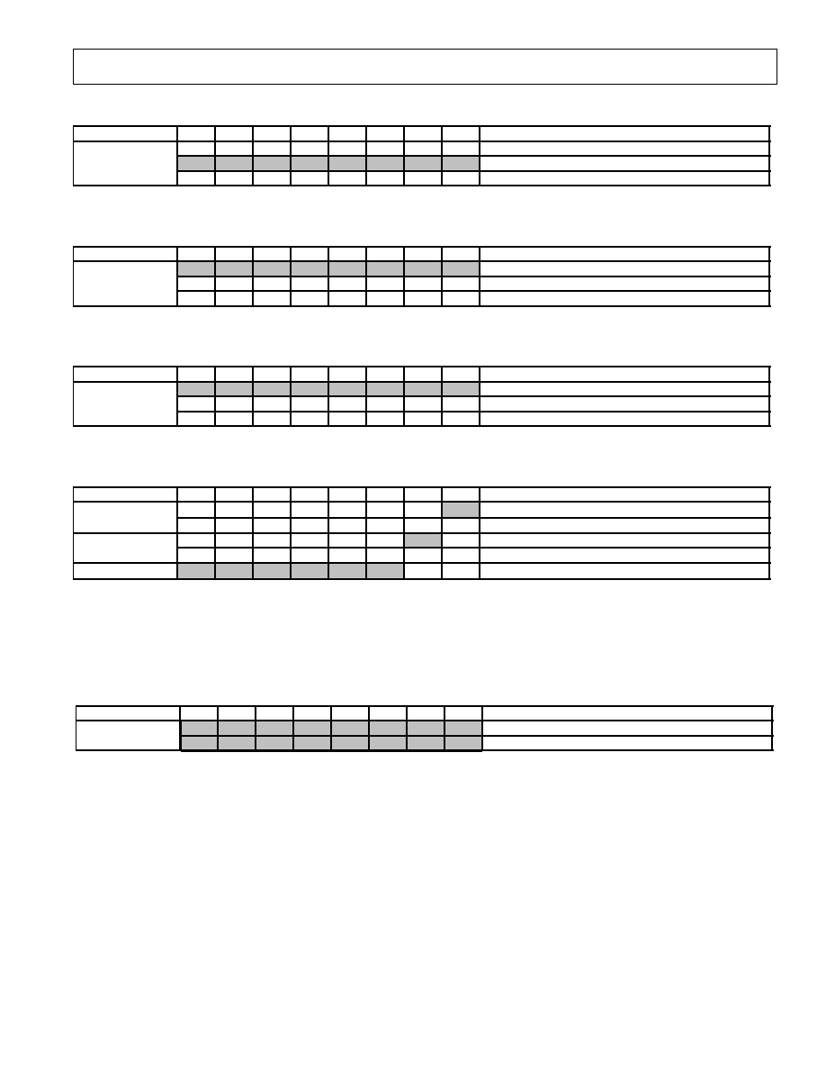
REV. 0
ADV7183
25
Table XIII. Saturation Adjust Register (Subaddress 09)
Bit Description Bit 7 Bit 6 Bit 5 Bit 4 Bit 3 Bit 2 Bit 1 Bit 0 Register Setting
SAT[7:0]
*
0
0
0
0
0
0
0
0
42 dB
1
0
0
0
0
0
0
0
0 dB
1
1
1
1
1
1
1
1
6 dB
*Saturation Adjust. Allows the user to adjust the saturation of color output.
Table XIV. Brightness Adjust Register (Subaddress 0A)
Bit Description Bit 7 Bit 6 Bit 5 Bit 4 Bit 3 Bit 2 Bit 1 Bit 0 Register Setting
BRI[7:0]
*
0
0
0
0
0
0
0
0
0 dB
0
1
1
1
1
1
1
1
3 dB
1
0
0
0
0
0
0
0
3 dB
*Controls the brightness of the video signal. Range =
± 3 dB.
Table XV. Hue Adjust Register (Subaddress 0B)
Bit Description Bit 7 Bit 6 Bit 5 Bit 4 Bit 3 Bit 2 Bit 1 Bit 0 Register Setting
HUE[7:0]
*
0
0
0
0
0
0
0
0
0°
0
1
1
1
1
1
1
1
90°
1
0
0
0
0
0
0
0
90°
*Contains the value for the color hue adjustment. Range =
± 90°.
Table XVI. Default Value Y Register (Subaddress 0C)
Bit Description Bit 7 Bit 6 Bit 5 Bit 4 Bit 3 Bit 2 Bit 1 Bit 0 Register Setting
DEF_ VAL_ EN
1
0
Use Programmed Value
2
1
Use Default Value
0
Use Programmed Value
4
1
Use Default Value
DEF_Y[5:0]
5
0
0
0
1
0
0
DEF_ VAL_
AUTO_EN
3
NOTES
1
Default Value Enable
2
Y, Cr, and Cb Values
3
Default Value Auto-Enable. In the case of lost lock enables/disables default values.
4
When lock is lost.
5
Default Value Y. Holds the Y default value.
Table XVII. Default Value C Register (Subaddress 0D)
Bit Description
Bit 7 Bit 6 Bit 5 Bit 4 Bit 3 Bit 2 Bit 1 Bit 0 Register Setting
DEF_C[7:0]
*
1
0
0
0
Cr[7:0] = {DEF_C[7:4], 0, 0, 0, 0}
1
0
0
0
Cb[7:0] = {DEF_C[3:0], 0, 0, 0, 0}
*Default Value C. Cr and Cb default values are defined in this register.
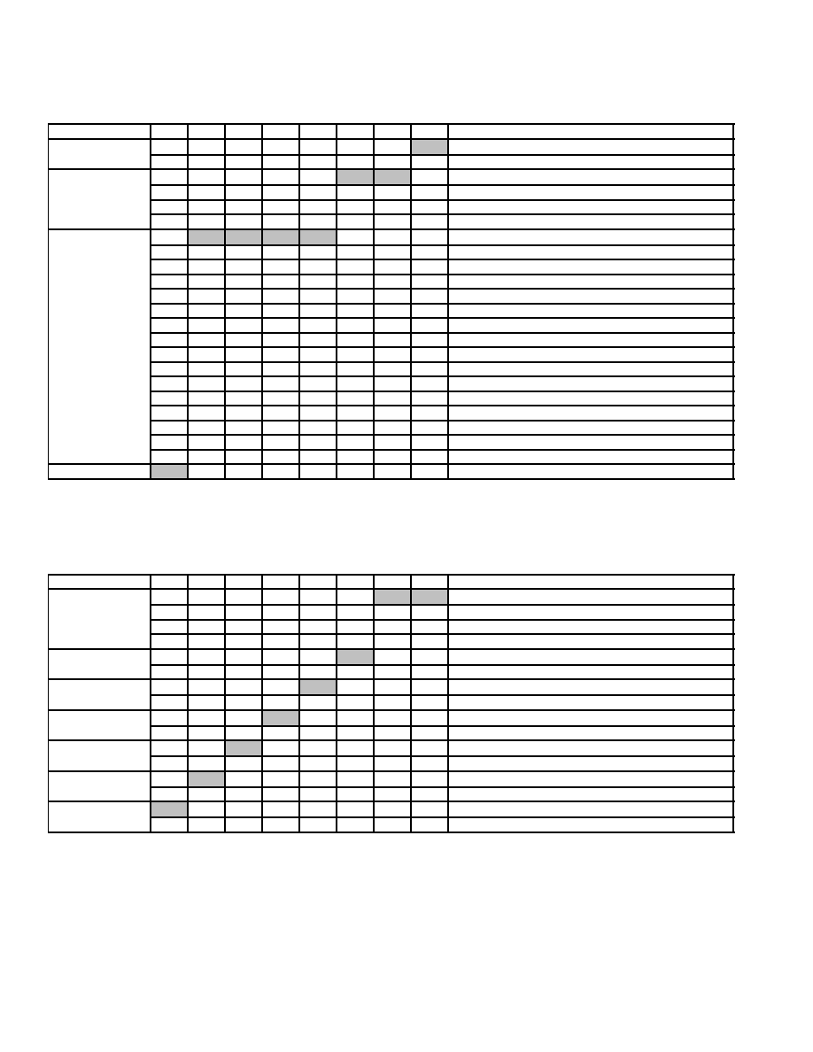
REV. 0
26
ADV7183
Table XVIII. Temporal Decimation Register (Subaddress 0E)
Bit Description Bit 7 Bit 6 Bit 5 Bit 4 Bit 3 Bit 2 Bit 1 Bit 0 Register Setting
TDE
1
0
Disabled
1
Enabled
TDC[1:0]
2
0
0
Suppress Frames; Start with Even Field
0
1
Suppress Frames; Start with Odd Field
1
0
Suppress Even Fields Only
1
1
Suppress Odd Fields Only
TDR[3:0]
3
0
0
0
0
Skip None
0
0
0
1
Skip 1 Field/Frame
0
0
1
0
Skip 2 Fields/Frames
0
0
1
1
Skip 3 Fields/Frames
0
1
0
0
Skip 4 Fields/Frames
0
1
0
1
Skip 5 Fields/Frames
0
1
1
0
Skip 6 Fields/Frames
0
1
1
1
Skip 7 Fields/Frames
1
0
0
0
Skip 8 Fields/Frames
1
0
0
1
Skip 9 Fields/Frames
1
0
1
0
Skip 10 Fields/Frames
1
0
1
1
Skip 11 Fields/Frames
1
1
0
0
Skip 12 Fields/Frames
1
1
0
1
Skip 13 Fields/Frames
1
1
1
0
Skip 14 Fields/Frames
1
1
1
1
Skip 15 Fields/Frames
RESERVED
0
Set to Zero
NOTES
1
Temporal Decimation Enable. Allows the user to enable/disable the temporal function. Configured using TDC[1:0] and TDR[3:0].
2
Temporal Decimation Control. Allows the user to select the suppression of selected fields of video.
3
Temporal Decimation Rate. Specifies how many fields/frames to be skipped before a valid one is output. As specified in the TDC[1:0] register.
Table XIX. Power Management Register (Subaddress 0F)
Bit Description Bit 7 Bit 6 Bit 5 Bit 4 Bit 3 Bit 2 Bit 1 Bit 0 Register Setting
PSC[1:0]
1
0
0
Full Operation
0
1
CVBS Input Only
1
0
Digital Only
1
1
Power Save Mode
PDBP
2
0
Power-Down Controller by Pin
1
Power-Down Controller by Bit
PS_REF
3
0
Reference Functional
1
Reference in Power Save Mode
PS_CG
4
0
Clock Generator Functional
1
CG in Power Save Mode
PWRDN
5
0
System Functional
1
Power-Down
TRAQ
6
0
Normal Operation
1
Require Video Signal
RESET
7
0
1
Resets Digital Core and I
2
C
NOTES
1
Power Save Control. Allows a set of different power save modes to be selected.
2
Power Down Bit Priority. There are two ways to shut down the digital core; the Power-Down Bit sets which has higher priority.
3
Power Save Reference. Allows the user to enable/disable the internal analog reference.
4
Power Save for the LLC Clock Generator
5
Power Down. Disables the input pads and powers down the 27 MHz clock.
6
Timing Reacquire. Will cause the part to reaquire the video signal and is the software version of the ISO pin. If bit is set will clear itself on the next 27 MHz clock
cycle.
7
Resets Digital Core and I
2
C self-clearing bit.
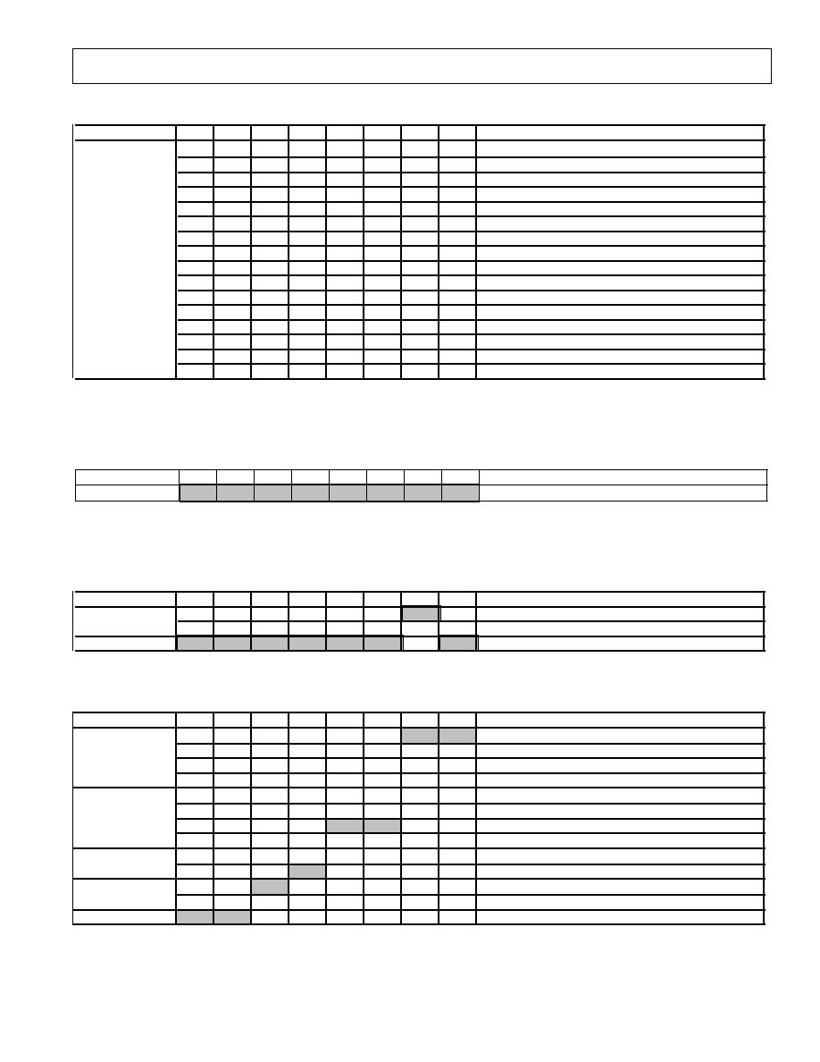
REV. 0
ADV7183
27
Table XX. Status Register
1
(Subaddress 10)
Bit Description
Bit 7 Bit 6 Bit 5 Bit 4 Bit 3 Bit 2 Bit 1 Bit 0 Register Setting
STATUS[7:0]
2
0
1
Color Kill Active
0
1
White Peak Active
0
1
ADC Overflow Detected
0
1
ADC Underflow Detected
0
1
50 Hz Field Rate Auto Detected
0
1
F
SC
Locked (current)
0
1
Lost Lock (since last read)
0
1
In Lock (current)
NOTES
1
Read only
2
Provides information about the internal status of the decoder.
Table XXI. Info Register
1
(Subaddress 11)
Bit Description
Bit 7 Bit 6 Bit 5 Bit 4 Bit 3 Bit 2 Bit 1 Bit 0 Register Setting
IDENT[7:0]
2
X
X
X
X
X
X
X
X
0 = v85a, 3 = v85b, 4 = v85b3, 5 = v85b3
NOTES
1
Read only
2
Provides identification on the revision of the part.
Table XXII. Analog Control Internal Register (Subaddress 13)
Bit Description
Bit 7 Bit 6 Bit 5 Bit 4 Bit 3 Bit 2 Bit 1 Bit 0 Register Setting
TIM_OE
*
0
Dependent on
OE and TOD
1
HS, VS, F Forced Active
RESERVED
0
1
0
0
0
1
1
Set at Default Value
*Timing Signals Output. Enables the user to force the output drivers for H-SYNC,V-SYNC, and Field into an active state regardless of the OE pin and TOD bit.
Table XXIII. Analog Clamp Control Register (Subaddress 14)
Bit Description Bit 7 Bit 6 Bit 5 Bit 4 Bit 3 Bit 2 Bit 1 Bit 0 Register Setting
FICL[1:0]
1
0
0
I On for 16 Clock Cycles
0
1
I On for 32 Clock Cycles
1
0
I On for 64 Clock Cycles
1
1
I On for 128 Clock Cycles
FACL[1:0]
2
0
0
I On for 16 Clock Cycles
0
1
I On for 32 Clock Cycles
1
0
I On for 64 Clock Cycles
1
1
I On for 128 Clock Cycles
CCLEN
3
0
I Sources Switched Off
1
I Sources Enabled
VCLEN
4
0
Voltage Clamp Disabled
1
Voltage Clamp Enabled
RESERVED
0
0
Set to Zero
NOTES
1
Fine Clamp Length. Controls the number of clock cycles for which the slow current is on.
2
Fast Clamp Length. Controls the number of clock cycles for which the fast current is on.
3
Current Clamp Enable. Allows the user to switch off the I sources in the analog front end.
4
Voltage Clamp Enable. Allows the user to disable the voltage clamp circuitry.
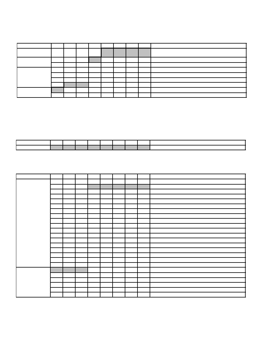
REV. 0
28
ADV7183
Table XXIV. Digital Clamp Control 1 Register (Subaddress 15)
Bit Description
Bit 7 Bit 6 Bit 5 Bit 4 Bit 3 Bit 2 Bit 1 Bit 0 Register Setting
DCCO[11:8]
1
X
X
X
X
Only applicable if DCCM is set to manual offset
mode.
DCFE
2
0
Digital Clamp Operational
1
Digital Clamp Frozen
DCT[1:0]
3
0
0
Slow (TC = 1 second)
0
1
Medium (TC = 0.5 second)
1
0
Fast (TC = 0.1 second)
1
1
Dependent on VID_QUAL
DCCM[7:0]
4
0
Automatic Digital Clamp
1
Manual Offset Correction
5
NOTES
1
Digital Color Clamp Offset. Holds upper 4 bits of the digital offset value which is added to the raw data from the ADC before entering the core.
2
Digital Clamp Freeze Enable. Allows the user to freeze the digital clamp loop at any point in time.
3
Digital Clamp Timing. Determines the time constant of the digital clamping circuitry.
4
Digital Color Clamp Mode. Sets the mode of operation for the digital clamp circuitry. Offset correction via DCCO for C only.
5
Offset Correction via DCCO for C only.
Table XXV. Digital Clamp Control 2 Register (Subaddress 16)
Bit Description Bit 7 Bit 6 Bit 5 Bit 4 Bit 3 Bit 2 Bit 1 Bit 0 Register Setting
DCCO[7:0]
*
X
X
X
X
X
X
X
X
*Digital Color Clamp Offset. Holds the lower 8 bits of the digital offset value which is added to the raw data from the ADC before entering the core. Only applicable if
DCCM is set to manual offset mode.
Table XXVI. Shaping Filter Control Register (Subaddress 17)
Bit Description Bit 7 Bit 6 Bit 5 Bit 4 Bit 3 Bit 2 Bit 1 Bit 0 Register Setting
YSFM[4:0]
1
0
0
0
0
0
Auto Wide Notch
0
0
0
0
1
Auto Narrow Notch
0
0
0
1
0
SVHS 1
1
0
0
1
0
SVHS 17
1
0
0
1
1
PAL NN1
1
0
1
0
0
PAL NN2
1
0
1
0
1
PAL NN3
1
0
1
1
0
PAL WN 1
1
0
1
1
1
PAL WN 2
1
1
0
0
0
NTSC NN1
1
1
0
0
1
NTSC NN2
1
1
0
1
0
NTSC NN3
1
1
0
1
1
NTSC WN1
1
1
1
0
0
NTSC WN2
1
1
1
0
1
NTSC WN3
1
1
1
1
0
Not Used
1
1
1
1
1
SVHS 18
CSFM[2:0]
2
0
0
0
Auto Selection 1.5 MHz
0
0
1
Auto Selection 2.17 MHz
0
1
0
SH1
1
1
0
SH5
1
1
1
SH6
NOTES
1
Y Shaping Filter Mode. Allows the user to select a wide range of low-pass and notch filters.
2
C Shaping Filter Mode. Allows the selection from a range of low-pass chrominance filters. Auto = filter selected based on scaling factor.
REV. 0
ADV7183
29
Table XXVII. Comb Filter Control Register (Subaddress 19)
Bit Description
Bit 7 Bit 6 Bit 5 Bit 4 Bit 3 Bit 2 Bit 1 Bit 0 Register Setting
RESERVED
0
0
0
0
0
Set to Zero
CCM[1:0]
1
0
0
No Comb
0
1
1H
1
0
2H
1
1
Not Valid, Do Not Use
CCMB_AD
2
0
Chroma Comb Nonadaptive
1
Chroma Comb Adaptive
NOTES
1
Chroma Comb Mode. Selects a primary mode for the filter.
2
Chroma Comb Adaptive
Table XXVIII. Color Subcarrier Control 1 Register (Subaddress 23)
Bit Description
Bit 7 Bit 6 Bit 5 Bit 4 Bit 3 Bit 2 Bit 1 Bit 0 Register Setting
CSMF[27:24]
1
X
X
X
X
CSM
2
0
Manual FSC Disabled
1
User Defined FSC
3
RESERVED
1
1
1
Set to One
NOTES
1
Color Subcarrier Manual Frequency. Holds the value used to enable the user to support odd subcarrier frequencies.
2
Color Subcarrier Manual
3
Defined in CSFM[27:0]
Table XXIX. Color Subcarrier Control 2 Register (Subaddress 24)
Bit Description Bit 7 Bit 6 Bit 5 Bit 4 Bit 3 Bit 2 Bit 1 Bit 0 Register Setting
CSMF[23:16]
*
X
X
X
X
X
X
X
X
*Color Subcarrier Manual Frequency. Holds the value used to enable the user to support odd subcarrier frequencies.
Table XXX. Color Subcarrier Control 3 Register (Subaddress 25)
Bit Description Bit 7 Bit 6 Bit 5 Bit 4 Bit 3 Bit 2 Bit 1 Bit 0 Register Setting
CSMF[15:8]
*
X
X
X
X
X
X
X
X
*Color Subcarrier Manual Frequency. Holds the value used to enable the user to support odd subcarrier frequencies.
Table XXXI. Color Subcarrier Control 4 Register (Subaddress 26)
Bit Description Bit 7 Bit 6 Bit 5 Bit 4 Bit 3 Bit 2 Bit 1 Bit 0 Register Setting
CSMF[7:0]
*
X
X
X
X
X
X
X
X
*Color Subcarrier Manual Frequency. Holds the value used to enable the user to support odd subcarrier frequencies.
REV. 0
30
ADV7183
Table XXXII. Pixel Delay Control Register (Subaddress 27)
Bit Description Bit 7 Bit 6 Bit 5 Bit 4 Bit 3 Bit 2 Bit 1 Bit 0 Register Setting
RESERVED
0
0
0
Set to Zero
CTA[2:0]
1
0
0
0
Not Valid
0
0
1
Chroma + 2 Pixel (Early)
0
1
0
Chroma + 1 Pixel (Early)
0
1
1
No Delay
1
0
0
Chroma 1 Pixel (Late)
1
0
1
Chroma 2 Pixel (Late)
1
1
0
Chroma 3 Pixel (Late)
1
1
1
Not Valid
RESERVED
1
Set to One
SWPC
2
0
No Swapping
1
Swap the Cr and Cb Values
NOTES
1
Chroma Timing Adjust. Allows a specified timing difference between the luma and chroma samples.
2
Allows the Cr and Cb samples to be swapped.
Table XXXIII. Manual Clock Control 1 Register (Subaddress 28)
Bit Description Bit 7 Bit 6 Bit 5 Bit 4 Bit 3 Bit 2 Bit 1 Bit 0 Register Setting
CLKVAL[17:16]
1
X
X
RESERVED
1
1
1
1
Set to Default
CLKMANE
2
0
Output Frequency Set by Video
1
Frequency Set by CLKVAL[17:0]
FIX27E
3
0
Output Frequency Set by Clock Generator
1
Output 27 MHz Fixed
NOTES
1
If enabled via CLKMANE, CLKVAL[17:0] determines the fixed output frequency. On the LLC, LLC2, and LLCREF pins.
2
Clock Generator Manual Enable. Allows the analog clock generator to produce a fixed clock frequency that is not dependent on the video signal.
3
Allows the o/p of fixed 27 MHz crystal clock via LLC, LLC2, and LLCR EF o/p pins.
Table XXXIV. Manual Clock Control 2 Register (Subaddress 29)
Bit Description Bit 7 Bit 6 Bit 5 Bit 4 Bit 3 Bit 2 Bit 1 Bit 0 Register Setting
CLKVAL[15:8]
* X
X
X
X
X
X
X
X
*If enabled via CLKMANE, CLKVAL[17:0] determines the fixed output frequency. On the LLC, LLC2, and LLCREF pins.
Table XXXV. Manual Clock Control 3 Register (Subaddress 2A)
Bit Description Bit 7 Bit 6 Bit 5 Bit 4 Bit 3 Bit 2 Bit 1 Bit 0 Register Setting
CLKVAL[7:0]
*
X
X
X
X
X
X
X
X
*If enabled via CLKMANE, CLKVAL[17:0] determines the fixed output frequency. On the LLC, LLC2, and LLCREF pins.
REV. 0
ADV7183
31
Table XXXVI. Auto Clock Control Register (Subaddress 2B)
Bit Description Bit 7 Bit 6 Bit 5 Bit 4 Bit 3 Bit 2 Bit 1 Bit 0 Register Setting
RESERVED
0
0
0
0
0
Set to Zero
ACLKN[2:0]
*
0
0
0
Color Burst Line
0
0
1
Start Line 24 Color Burst Line
0
1
0
Active Video
0
1
1
Active Video (<304) PAL, (<264) NTSC
1
0
0
Active Video (<304) PAL, (<256) NTSC
1
0
1
Active Video (<319/320) PAL, (<273/274) NTSC
1
1
0
Invalid
1
1
1
Invalid
*Automatic Clock Generator Mode. Influences the mode of operation for the LLC. Only when not in Manual Mode.
Table XXXVII. AGC Mode Control Register (Subaddress 2C)
Bit Description
Bit 7 Bit 6 Bit 5 Bit 4 Bit 3 Bit 2 Bit 1 Bit 0 Register Setting
CAGC[1:0]
1
0
0
Manual Fixed Gain; use CMG [11:0]
0
1
Use Luma Gain for Chroma
1
0
Automatic Gain; Based on Color Burst
1
1
Freeze Chroma Gain
RESERVED
1
1
Set to One
LAGC[2:0]
2
0
0
0
Manual Fixed Gain
3
0
0
1
AGC No Override through White Peak; Manual IRE
Control
4
0
1
0
AGC Auto Override through White Peak; Manual
IRE Control
4
0
1
1
AGC No Override through White Peak; Manual IRE
Control
4
1
0
0
AGC Auto Override through White Peak; Manual
IRE Control
4
1
0
1
AGC Active Video with White Peak
1
1
0
AGC Active Video with Average Video
1
1
1
Freeze Gain
RESERVED
1
Set to One
NOTES
1
Chroma Automatic Gain Control. Selects the basic mode of operation for the AGC in the chroma path.
2
Luma Automatic Gain Control. Selects the mode of operation for the gain control in the luma path.
3
Use LMG[11:0].
4
Blank level to sync tip.
Table XXXVIII. Chroma Gain Control 1 Register (Subaddress 2D)
Bit Description
Bit 7 Bit 6 Bit 5 Bit 4 Bit 3 Bit 2 Bit 1 Bit 0 Register Setting
CMG[11:8]
1
X
X
X
X
RESERVED
1
1
Set to One
CAGT[1:0]
2
0
0
Slow (TC = 2 sec)
0
1
Medium (TC = 1 sec)
1
0
Fast (TC = 0.2 sec)
1
1
Dependent on VID_QUAL
NOTES
1
Chroma Manual Gain. Can be used to program a desired manual chroma gain or read back the actual used gain value. CAGC[1:0] settings will decide in which mode
CMG[11:0] will operate.
2
Chroma Automatic Gain Timing. Allows adjustment of the Chroma AGC tracking speed. Will only have effect if CAGC[1:0] is set to auto gain (10b).
Table XXXIX. Chroma Gain Control 2 Register (Subaddress 2E)
Bit Description Bit 7 Bit 6 Bit 5 Bit 4 Bit 3 Bit 2 Bit 1 Bit 0 Register Setting
CMG[7:0]
*
X
X
X
X
X
X
X
X
*Chroma Manual Gain. Lower 8 bits, see CMG [11:8] for description.
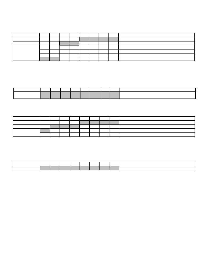
REV. 0
32
ADV7183
Table XL. Luma Gain Control 1 Register (Subaddress 2F)
Bit Description
Bit 7 Bit 6 Bit 5 Bit 4 Bit 3 Bit 2 Bit 1 Bit 0 Register Setting
LMG[11:8]
1
X
X
X
X
RESERVED
1
1
Set to One
LAGT[1:0]
2
0
0
Slow (TC = 2 sec)
0
1
Medium (TC = 1 sec)
1
0
Fast (TC = 0.2 sec)
1
1
Dependent on VID_QUAL
NOTES
1
Luma Manual Gain. Can be used to program a desired manual chroma gain or read back the actual used gain value. LAGC[1:0] settings will decide in which mode
LMG[11:0] will operate.
2
Luma Automatic Gain Timing. Allows adjustment of the Luma AGC tracking speed. Will only have effect if LAGC[1:0] is set to auto gain (001, 010, 001, or 100).
Table XLI. Luma Gain Control 2 Register (Subaddress 30)
Bit Description
Bit 7 Bit 6 Bit 5 Bit 4 Bit 3 Bit 2 Bit 1 Bit 0 Register Setting
LMG[7:0]
*
X
X
X
X
X
X
X
X
LAGC [1:0] Settings Will Decide What
Mode LMG [11:0] Operates In.
*Luma Manual Gain. Can be used to program a desired manual chroma gain or read back the actual used gain value.
Table XLII. Manual Gain Shadow Control 1 Register (Subaddress 31)
Bit Description Bit 7 Bit 6 Bit 5 Bit 4 Bit 3 Bit 2 Bit 1 Bit 0 Register Setting
LMGS[11:8]
1
X
X
X
X
RESERVED
1
1
1
Set to One
SGUE
2
0
Disable LMGS Update
1
Use LMGS Update Facility
NOTES
1
Luma Manual Gain Store. Has dual functions; a desired manual luma gain can be programmed or a readback from the register will return the actual gain used. Gain
value will only become active when LAGC[2:0] set to manual fixed gain. The function and readback value are dependent on LAGC[2:0] setting.
2
Surveillance Gain Update Enable. Enables surveillance mode operation (see LMGS[11:0] for details).
Table XLIII. Manual Gain Shadow Control 2 Register (Subaddress 32)
Bit Description Bit 7 Bit 6 Bit 5 Bit 4 Bit 3 Bit 2 Bit 1 Bit 0 Register Setting
LMG[7:0]
*
X
X
X
X
X
X
X
X
*Chroma Manual Gain. Lower 8 bits, see LMG[11:8] for description.
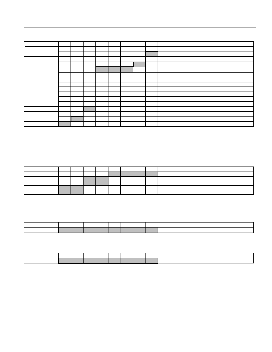
REV. 0
ADV7183
33
Table XLIV. Miscellaneous Gain Control Register (Subaddress 33)
Bit Description
Bit 7 Bit 6 Bit 5 Bit 4 Bit 3 Bit 2 Bit 1 Bit 0 Register Setting
PW_UPD
1
0
Update Gain Once per Line
1
Update Gain Once per Field
AV_AL
2
0
Lines 33 to 310
1
Lines 33 to 270
MIRE[2:0]
3
0
0
0
PAL-133 NTSC-122
0
0
1
PAL-125 NTSC-115
0
1
0
PAL-120 NTSC-110
0
1
1
PAL-115 NTSC-105
1
0
0
PAL-110 NTSC-100
1
0
1
PAL-105 NTSC-100
1
1
0
PAL-100 NTSC-100
1
1
1
PAL-100 NTSC-100
RESERVED
1
Set to One
CKE
0
Color Kill Disabled
1
Color Kill Enabled
RESERVED
1
Set to One
4
NOTES
1
Peak White Update. Determines the gain based on measurements taken from the active video; this bit determines the rate of gain change. LAGC[1:0] must be set to
the appropriate mode to enable peak white or average video in the first case.
2
Average Brightness Active Lines. Allows the selection between two ranges of active video to determine the average brightness.
3
Max IRE. Sets the max I/p IRE level depending on the video standard.
4
Color Kill Enable. Allows the optional color kill function to be switched on or off.
Table XLV. HSync Position Control 1 Register (Subaddress 34)
Bit Description Bit 7 Bit 6 Bit 5 Bit 4 Bit 3 Bit 2 Bit 1 Bit 0 Register Setting
RESERVED
1
1
1
1
Set to One
HSE[9:8]
1
0
0
HSync ends after HSE[9:0] pixel after falling edge
of HSync.
HSB[9:8]
2
0
0
HSync starts after HSB[9:0] pixel after the falling
edge of HSync.
NOTES
1
HSync End. Allows the positioning of the HSync output within the video line.
2
HSync Begin. Allows the positioning of HSync output within the video line.
Table XLVI. HSync Position Control 2 Register (Subaddress 35)
Bit Description
Bit 7 Bit 6 Bit 5 Bit 4 Bit 3 Bit 2 Bit 1 Bit 0 Register Setting
HSB[7:0]
0
0
0
0
0
0
0
1
1
1
Using HSB[9:0] and HSE[9:0] the user can program the position and length of HSync output signal.
Table XLVII. HSync Position Control 3 Register (Subaddress 36)
Bit Description
Bit 7 Bit 6 Bit 5 Bit 4 Bit 3 Bit 2 Bit 1 Bit 0 Register Setting
HSE[7:0]
0
0
0
0
0
0
0
1
1
1
Using HSB[9:0] and HSE[9:0] the user can program the position and length of HSync output signal.
REV. 0
34
ADV7183
Table XLVIII. Polarity Register (Subaddress 37)
Bit Description Bit 7 Bit 6 Bit 5 Bit 4 Bit 3 Bit 2 Bit 1 Bit 0 Register Setting
PCLK
1
0
Active High
1
Active Low
PFF
2
0
Active High
1
Active Low
PDV
3
0
Active High
1
Active Low
PF
4
0
Active High
1
Active Low
PLLCR
5
0
Active High
1
Active Low
PVS
6
0
Active High
1
Active Low
PHVR
7
0
Active High
1
Active Low
PHS
8
0
Active High
1
Active Low
NOTES
1
Sets the polarity of LLC, LLC2, and QClk.
2
Sets the polarity of HFF, AEF, and AFF.
3
Sets the polarity for Data Field.
4
Sets the field sync polarity.
5
Sets the LLCREF polarity.
6
Sets the VSync polarity.
7
Sets the HREF and VREF sync polarities.
8
Sets HSync Polarity.
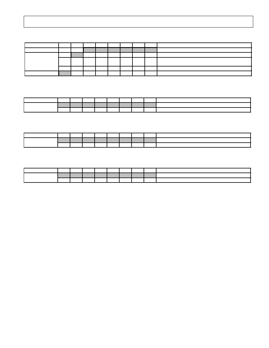
REV. 0
ADV7183
35
Table XLIX. Resample Control Register (Subaddress 44)
Bit Description
Bit 7 Bit 6 Bit 5 Bit 4 Bit 3 Bit 2 Bit 1 Bit 0 Register Setting
RESERVED
0
0
0
0
0
1
Set to Default
FSC_INV
*
X
NB No Default Value < v85c
0
Compatible with ADV7190, ADV7191, and
ADV7194
1
Compatible with ADV717x
RESERVED
0
Set to Zero
*Color Subcarrier RTCO Inversion. Allows the inversion of the GL bit.
Table L. Reserved (Subaddress 45)
Bit Description Bit 7 Bit 6 Bit 5 Bit 4 Bit 3 Bit 2 Bit 1 Bit 0 Register Setting
0
0
1
X
X
0
1
1
Default Values
1
0
1
1
1
0
1
1
Set to These Values
Reserved
Functions
Table LI. Reserved (Subaddress F1)
Bit Description Bit 7 Bit 6 Bit 5 Bit 4 Bit 3 Bit 2 Bit 1 Bit 0 Register Setting
1
1
1
1
0
1
1
X
Default Values
1
1
1
0
1
1
1
1
Set to These Values
Reserved
Functions
Table LII. Reserved (Subaddress F2)
Bit Description Bit 7 Bit 6 Bit 5 Bit 4 Bit 3 Bit 2 Bit 1 Bit 0 Register Setting
1
0
0
1
1
1
0
X
Default Values
1
0
0
0
0
0
0
0
Set to These Values
Reserved
Functions

REV. 0
36
ADV7183
Addr
Default
Register
(Hex)
(Hex)
BASIC BLOCK
Input Control
00
00
Video Selection
01
80
Video Enhancement Control
02
04
Output Control
03
0C
Extended Output Control
04
0C
General-Purpose Output
05
40
Reserved
06
XX
FIFO Control
07
04
Contrast Control
08
80
Saturation Control
09
80
Brightness Control
0A
0
Hue Control
0B
0
Default Value Y
0C
10
Default Value C
0D
88
Temporal Decimation
0E
00
Power Management
0F
00
Status Register
10
Info Register
11
Table LIII. Power-On Reset Values for MPU Registers
Addr
Default
Register
(Hex)
(Hex)
ADVANCED BLOCK
Reserved
12
XX
Analog Control (Internal)
13
45
Analog Clamp Control
14
18
Digital Clamp Control 1
15
6X
Digital Clamp Control 2
16
XX
Shaping Filter Control
17
01
Reserved
18
XX
Comb Filter Control
19
10
Reserved
1A
XX
Reserved
1B
XX
Reserved
1C
XX
Reserved
1D
XX
Reserved
1E
XX
Reserved
1F
XX
Reserved
20
XX
Reserved
21
XX
Reserved
22
XX
Color Subcarrier Control 1
23
EX
Color Subcarrier Control 2
24
XX
Color Subcarrier Control 3
25
XX
Color Subcarrier Control 4
26
XX
Pixel Delay Control
27
58
Manual Clock Control 1
28
XX
Manual Clock Control 2
29
XX
Manual Clock Control 3
2A
XX
Auto Clock Control .
2B
A0
AGC Mode Control
2C
CE
Chroma Gain Control 1
2D
FX
Chroma Gain Control 2
2E
XX
Luma Gain Control 1
2F
FX
Luma Gain Control 2
30
XX
Manual Gain Shadow Control 1
31
7X
Manual Gain Shadow Control 2
32
XX
Miscellaneous Gain Control
33
E3
Hsync Position Control 1
34
0F
Hsync Position Control 2
35
01
Hsync Position Control 3
36
00
Polarity Control
37
00
Reserved
44
X1
Reserved
45
XX
Reserved
F1
FX
Reserved
F2
9X

REV. 0
ADV7183
37
Appendix
BOARD DESIGN AND LAYOUT CONSIDERATIONS
The ADV7183 is a highly integrated circuit containing both preci-
sion analog and high-speed digital circuitry. It has been designed to
minimize interference effects on the integrity of the analog circuitry
by the high-speed digital circuitry. It is imperative that these same
design and layout techniques be applied to the system level design
such that high speed and accurate performance are achieved. Figure
30 shows the recommended analog circuit layout.
The layout should be optimized for lowest noise on the ADV7183
power and ground lines by shielding the digital inputs and provid-
ing good decoupling. The lead length between groups of VDD and
GND pins should be minimized to reduce inductive ringing.
Ground Planes
The ground plane should be split into two, one analog and one
digital. They should be joined directly under the ADV7183.
The analog ground return path should be through the digital
(the digital ground is connected to the analog ground and also
the system ground, whereas the analog ground is only connected
to the digital ground; this will ensure only analog current will flow
in the analog ground).
Power Planes
The ADV7183 and any associated analog circuitry should have
its own power planes, referred to as the analog and digital
power planes. These power planes should be connected to the
regular PCB power plane (V
CC
) at a single point through a ferrite
bead. This bead should be located within three inches of the
ADV7183.
The PCB power plane should provide power to all digital logic on
the PC board and the digital power pins on the ADV7183, and
the analog power plane should provide power to all analog power
pins on the ADV7183.
Plane-to-plane noise coupling can be reduced by ensuring that
portions of the regular PCB power and ground planes do not
overlay portions of the analog power plane, unless they can be
arranged so the plane-to-plane noise is common-mode.
Supply Decoupling
For optimum performance, bypass capacitors should be installed
using the shortest leads possible, consistent with reliable operation,
to reduce the lead inductance. Best performance is obtained with
0.1
µF ceramic capacitor decoupling. Each group of power pins
on the ADV71783 must have at least one 0.1
µF decoupling
capacitor to its corresponding ground. These capacitors should
be placed as close as possible to the device.
It is important to note that while the ADV7183 contains cir-
cuitry to reject power supply noise, this rejection decreases with
frequency. If a high-frequency switching power supply is used,
the designer should pay close attention to reducing power sup-
ply noise and consider using a three-terminal voltage regulator
for supplying power to the analog power plane.
Digital Signal Interconnect
The digital inputs and outputs to and from the ADV7183 should
be isolated as much as possible from the analog inputs and other
analog circuitry. Also, these input signals should not overlay the
analog power plane.
Due to the high clock rates involved, long clock lines to and
from the ADV7183 should be avoided to reduce noise pickup.
Any series termination resistors (typically 33
) for the digital
inputs should be connected to the high-speed digital outputs.
Analog Signal Interconnect
The ADV7183 should be located as close as possible to the
input connectors to minimize noise pickup and reflections due
to impedance mismatch.
The video input signals should overlay the ground plane, and
not the analog power plane, to maximize the high-frequency
power supply rejection.
Digital outputs, especially pixel data Inputs and clocking sig-
nals, should never overlay any of the analog signal circuitry and
should be kept as far away as possible.
The ADV7183 should have no inputs left floating. Any inputs
that are not required should be tied to ground.
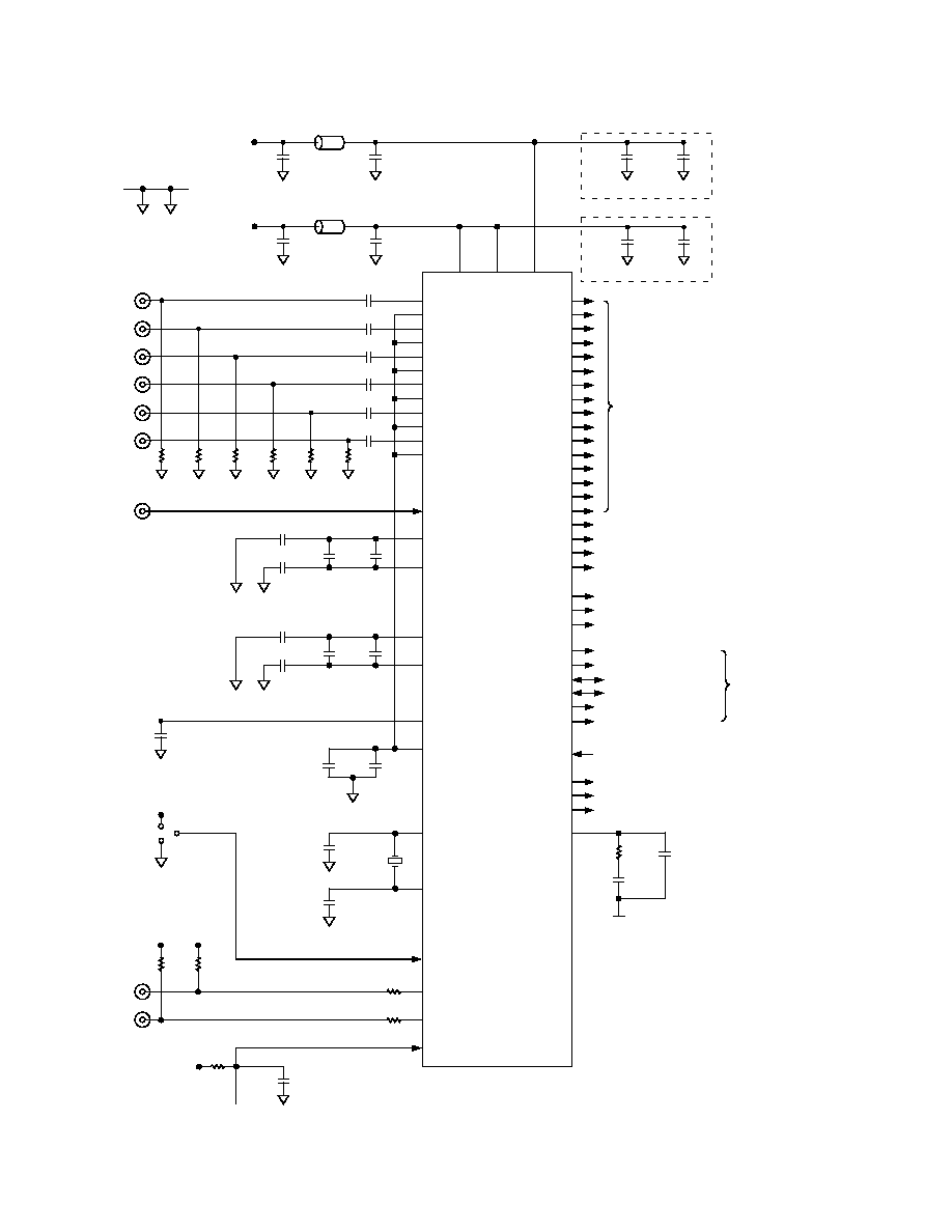
REV. 0
38
ADV7183
AIN1
AIN2
AIN3
AIN4
AIN5
AIN6
AVSS
AVSS
AVSS
AVSS
AVSS
AVSS
100nF
100nF
100nF
100nF
100nF
100nF
AIN1
AIN2
AIN3
AIN4
AIN5
AIN6
AVSS6
AVSS5
AVSS4
AVSS3
AVSS2
AVSS1
DVDDIO DVDD
AVDD
P0
P2
P4
P6
P8
P10
P11
P9
P7
P5
P3
P1
P12
P14
GPO0
GPO2
GPO3
GPO1
P15
P13
DVDD
FERRITE
BEAD
33 F
10 F
DVSS
DVSS
AVDD
FERRITE
BEAD
33 F
10 F
AVSS
AVSS
AVSS DVSS
0.1 F
0.01 F
DVSS
DVSS
0.1 F
0.01 F
AVSS
AVSS
POWER SUPPLY DECOUPLING
FOR EACH POWER PIN
POWER SUPPLY DECOUPLING
FOR EACH POWER PIN
INPUT
SWITCH OVER
ISO
10 F
0.1 F
0.1 F
0.1 F
AVSS
AVSS
10 F
0.1 F
0.1 F
0.1 F
AVSS
AVSS
CAP Y1
CAP Y2
CAP C1
CAP C2
0.1 F
CML
REFOUT
10 F
0.1 F
AVSS
XTAL
XTAL1
33 F
33 F
27MHz
DVSS
DVSS
DVSS
DVDD
ALSB
SCLK
SDA
RESET
I
2
C INTERFACE
CONTROL LINE
I
2
C INTERFACE
CONTROL LINE
100R
100R
2k
2k
DVDD
DVDD
100nF
DVSS
DVDD
RESET
MULTIFORMAT
PIXEL PORT*
P15P8: 8-BIT CCIR656 PIXEL DATA @ 27MHz
P7P0: Cb AND Cr 16-BIT CCIR656 PIXEL DATA @ 13.5MHz
P15P8: Y1 AND Y2 16-BIT CCIR656 PIXEL DATA @ 13.5MHz
*
LLC2
LLCREF
LLC
AEF
RD
DV
GL/QCLK/HFF
OE
AFF
27MHz OUTPUT CLOCK
13.5MHz OUTPUT CLOCK
CLOCK REFERENCE O/P
ALMOST EMPTY FIFO O/P
ALMOST FULL FIFO O/P
READ SIGNAL I/P
OUTPUT ENABLE I/P
DATA VALID O/P
GL/QCLK/HFF O/P
VS/
RESET
FIELD
HS/
RESET
HS/
RESET O/P
VS/
RESET O/P
FIELD O/P
PWRDN
POWER-DOWN INPUT
FIFO MANAGEMENT
SIGNALS ONLY USED
IN FIFO MODE;
USE LLC AND GENLOCK
FOR NON-FIFO MODE
ELPF
5.6k
2nF
68pF
AVDD
4.7k
Figure 30. Recommended Analog Circuit Layout
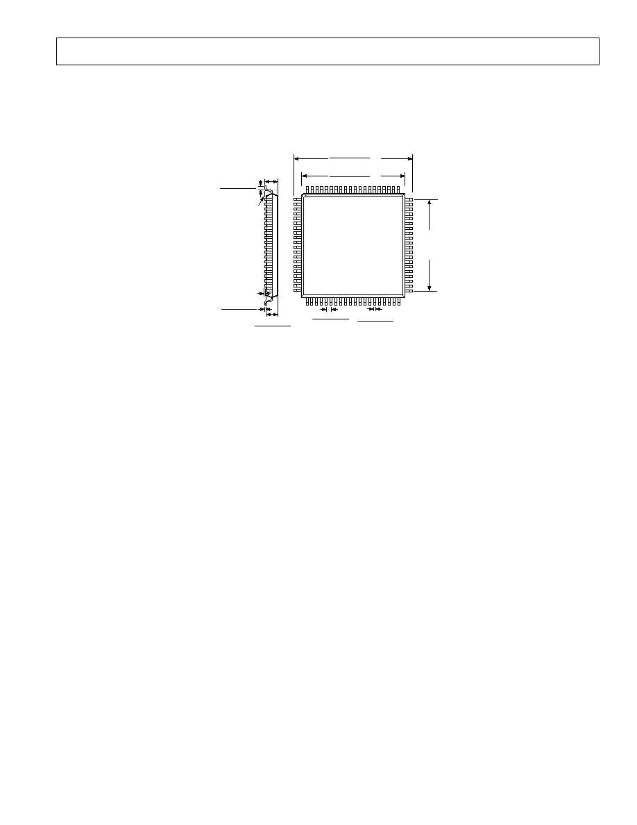
REV. 0
ADV7183
39
OUTLINE DIMENSIONS
Dimensions shown in millimeters and (inches)
80-Lead Thin Plastic Quad Flatpack [LQFP]
(ST-80)
TOP VIEW
(PINS DOWN)
1
20
21
41
40
60
61
80
16.25 (0.6398)
15.75 (0.6201)
SQ
14.05 (0.5532)
13.95 (0.5492)
SQ
0.35 (0.0138)
0.25 (0.0098)
0.73 (0.0287)
0.57 (0.0224)
12.35
(0.4862)
TYP
SQ
1.60 (0.0630)
MAX
0.75 (0.0295)
0.50 (0.0197)
SEATING
PLANE
0.15 (0.0059)
0.05 (0.0020)
0.10 (0.0039)
MAX
1.45 (0.0571)
1.35 (0.0531)
COPLANARITY
CONTROLLING DIMENSIONS ARE IN MILLIMETERS; INCH DIMENSIONS
(IN PARENTHESES) ARE ROUNDED-OFF MILLIMETER EQUIVALENTS FOR
REFERENCE ONLY AND ARE NOT APPROPRIATE FOR USE IN DESIGN

C0168205/02(0)
PRINTED IN U.S.A.
40
ADV7183

This datasheet has been download from:
www.datasheetcatalog.com
Datasheets for electronics components.