 | ÐлекÑÑоннÑй компоненÑ: ADV7185 | СкаÑаÑÑ:  PDF PDF  ZIP ZIP |
Äîêóìåíòàöèÿ è îïèñàíèÿ www.docs.chipfind.ru
REV. 0
a
Information furnished by Analog Devices is believed to be accurate and
reliable. However, no responsibility is assumed by Analog Devices for its
use, nor for any infringements of patents or other rights of third parties that
may result from its use. No license is granted by implication or otherwise
under any patent or patent rights of Analog Devices.
One Technology Way, P.O. Box 9106, Norwood, MA 02062-9106, U.S.A.
Tel: 781/329-4700
www.analog.com
Fax: 781/326-8703
© Analog Devices, Inc., 2002
ADV7185
Professional NTSC/PAL Video Decoder
with 10-Bit CCIR656 Output
ADLLT is a trademark and ADV is a registered trademark of Analog Devices, Inc.
FEATURES
Analog Video to Digital YCrCb Video Decoder:
NTSC-(M/N), PAL-(B/D/G/H/I/M/N)
ADV
®
7185 Integrates Two 12-Bit ADCs
Clocked from a Single 27 MHz Crystal
Dual Video Clocking Schemes:
Line-Locked Clock Compatible (LLC)
Adaptive Digital Line Length Tracking (ADLLTTM)
3-Line Chroma Comb Filter
Real-Time Clock and Status Information Output
Integrated AGC (Automatic Gain Control) and Clamping
Multiple Programmable Analog Input Formats:
CVBS (Composite Video)
SVHS (Y/C)
YCrCb Component (VESA, MII, SMPTE, and BetaCam)
6 Analog Input Video Channels
Real-Time Horizontal and Vertical Scaling
Automatic NTSC/PAL Identification
Differential Mode Video Input
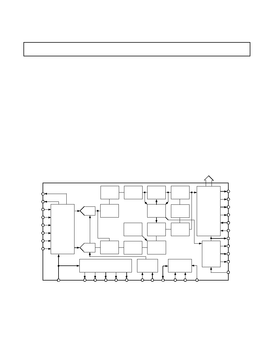
FUNCTIONAL BLOCK DIAGRAM
ISO
REFOUT
AIN1
AIN2
AIN3
AIN4
AIN5
AIN6
ANALOG I/P
MULTIPLEXING
AUTOMATIC
GAIN
CONTROL
(AGC)
CLAMP AND
DC RESTORE
12-BIT
ADC
LUMA
ANTIALIAS
LPF
SHAPING
AND
NOTCH LPF
PEAKING
HPF/LPF
RESAMPLING
AND
HORIZONTAL
SCALING
SYNC
DETECTION
ADV7185
RESAMPLING
AND
HORIZONTAL
SCALING
CHROMA
ANTIALIAS
LPF
SHAPING
LPF
SWITCH
LUMA
DELAY
BLOCK
2H LINE
MEMORY
SUB-
CARRIER
RECOVERY
DTO
12-BIT
ADC
27MHz
VIDEO TIMING AND
CONTROL BLOCK
27MHz XTAL
OSCILLATOR
BLOCK
PWRDN
HSYNC FIELD VSYNC HREF
VREF
CLOCK
CLOCK
AFF
HFF/QCLK
AEF
DV
RD
OE
FIFO CONTROL
BLOCK
AND
PIXEL
OUTPUT
FORMATTER
LLC
SYNTHESIS
WITH LINE-
LOCKED
OUTPUT
CLOCK
I
2
C-COMPATIBLE
INTERFACE PORT
SDATA SCLOCK
RESET
ALSB
GL/CLKIN
LLC1
LLC2
LLCREF
ELPF
P19P0
PIXEL
O/P PORT
CHROMA
COMB
FILTER
Digital Output Formats (20-Bit Wide Bus):
YCrCb (4:2:2 or 4:1:1)
CCIR601/CCIR656 8-Bit or Extended 10-Bit
0.5 V to 2.0 V p-p Input Range
Differential Gain, 0.4% Typ
Differential Phase, 0.6
o
Typ
Programmable Video Controls:
Peak White/Hue/Brightness/Saturation/Contrast
CCIR/Square/4 F
SC
Pixel Operation
APPLICATIONS
Projectors
Digital TVs
DVD-RAM Recorders and Players
PDP Displays
Video Decoders
Hybrid Analog/Digital Set-Top Boxes
Professional Equipment
(continued on page 9)
REV. 0
2
ADV7185SPECIFICATIONS
1
(V
AA
= 4.75 V to 5.25 V, V
DD
= 3.2 V to 3.5 V, V
DDIO
= 3.15 V to 3.5 V, T
MIN
to T
MAX
2
,
unless otherwise noted.)
Parameter
Min
Typ
Max
Unit
Test Conditions
STATIC PERFORMANCE
Resolution (each ADC)
12
Bits
12-Bit Range
Accuracy (each ADC)
Integral Nonlinearity
3
±0.5
±1.0
LSB
BSL, 2 V Input Captured in a 10-Bit
Range
Differential Nonlinearity
3
±0.175 ±0.325
LSB
2 V Input Captured in a 10-Bit Range
DIGITAL INPUTS
3
Input High Voltage, V
INH
2
V
Input Low Voltage, V
INL
0.8
V
V
IN
= 0.4 V or 2.4 V
Input Current, I
IN
10
+10
µA
Input Capacitance, C
IN
10
pF
DIGITAL OUTPUTS
3
Output High Voltage, V
OH
2.4
V
I
SOURCE
= 3.2 mA
Output Low Voltage, V
OL
0.4
V
I
SINK
= 0.4 mA
High Impedance Leakage Current
10
µA
Output Capacitance
30
pF
VOLTAGE REFERENCE
3
Reference Range, V
REFOUT
2.15
2.2
2.25
V
I
VREFOUT
= 0
µA
POWER REQUIREMENTS
Digital Power Supply, V
DD
3.2
3.3
3.5
V
Digital IO Power Supply, V
DDIO
3.15
3.3
3.5
V
Analog Power Supply, V
AA
4.75
5.0
5.25
V
Digital Supply Current, I
DD
125
165
mA
Digital IO Supply Current, I
DDIO
7
mA
Analog Supply Current, I
AA
4
150
180
mA
Power-Up Time
1
Field
Sleep Mode until Powered Up
NOTES
1
The max/min specifications are guaranteed over this range. The max/min values are typical over V
AA
= 4.75 V to 5.25 V, V
DD
= 3.2 V to 3.5 V, and V
DDIO
= 3.15 V to
3.5 V range.
2
Temperature Range T
MIN
to T
MAX
= 0
°C to 70°C
3
Guaranteed by characterization.
4
I
AA
is total analog current taken by AVDD supply pins.
Specifications subject to change without notice.
REV. 0
ADV7185
3
VIDEO PERFORMANCE SPECIFICATIONS
1, 2
Parameter
Min
Typ
Max
Unit
Test Conditions
NONLINEAR SPECIFICATIONS
2
Differential Phase
0.4
Degree
CVBS, Comb/No Comb
Differential Gain
0.6
%
CVBS, Comb/No Comb
Luma Nonlinearity
0.5
%
NOISE SPECIFICATIONS
2
SNR (Ramp)
61
63
dB
CVBS
Analog Front End Channel Crosstalk
63
dB
S-Video/YUV, Single-Ended
63
dB
S-Video/YUV, Differential-Ended
LOCK TIME AND JITTER
SPECIFICATIONS
2
Horizontal Lock Time
50
Lines
TV/VCR Mode
Horizontal Recovery Time
50
Lines
Horizontal Lock Range
±5
%
Line Length Variation Over Field
±1
%
VCR Mode/Surveillance Mode
±1
%
TV Mode
HLock Lost Declared
10
HSync
TV Mode, Number of Missing HSyncs
20
HSync
VCR/Surveillance Mode, Number of
Missing HSyncs
Vertical Lock Time
2
VSync
First Lock into Video Signal
VLock Lost Declared
1
VSync
All Modes, Number of Missing VSyncs
F
SC
Subcarrier Lock Range
±400
Hz
NTSC/PAL
Color Lock Time
50
Lines
HLock to Color Lock Time
LLC Clock Jitter (Short Time Jitter)
1
ns
RMS Clock Jitter
LLC Clock Jitter (Frame Jitter)
37
ns
RMS Clock Jitter
CHROMA-SPECIFIC
SPECIFICATIONS
2
Hue Accuracy
0.5
Degree
Color Saturation Accuracy
0.6
%
Color Gain Control Range
6
+18
dB
S-Video, YUV, Overall CGC Range
(Analog and Digital)
Analog Color Gain Range
6
+6
dB
S-Video, YUV
Digital Color Gain Range
0
12
dB
CVBS, S-Video, YUV
Chroma Amplitude Error
0.1
%
Chroma Phase Error
0
Degree
Chroma Luma Intermodulation
0.1
%
LUMA-SPECIFIC SPECIFICATIONS
2
Luma Brightness Accuracy
1.0
%
Video Input Range = 1.0 V p-p
Luma Contrast Accuracy
1.0
%
Video Input Range = 1.0 V p-p
NOTES
1
The max/min specifications are guaranteed over this range. The max/min values are typical over V
AA
= 4.75 V to 5.25 V, V
DD
= 3.2 V to 3.5 V, and V
DDIO
= 3.15 V to
3.5 V range.
2
Guaranteed by characterization.
3
Temperature range T
MIN
to T
MAX
= 0
°C to 70°C
Specifications subject to change without notice.
(V
AA
= 4.75 V to 5.25 V, V
DD
= 3.2 V to 3.5 V, V
DDIO
= 3.15 V to 3.5 V,
T
MIN
to T
MAX
3
, unless otherwise noted.)
REV. 0
4
ADV7185
TIMING SPECIFICATIONS
1
Parameter
Min
Typ
Max
Unit
Test Conditions
SYSTEM CLOCK AND CRYSTAL
Nominal Frequency
27
MHz
I
2
C PORT
3
SCL Clock Frequency
0
400
kHz
SCL Min Pulsewidth High, t
1
0.6
µs
SCL Min Pulsewidth Low, t
2
1.3
µs
Hold Time (Start Condition), t
3
0.6
µs
Setup Time (Start Condition), t
4
0.6
µs
Data Setup Time, t
5
100
ns
SCL/SDA Rise Time, t
6
300
ns
SCL/SDA Fall Time, t
7
300
ns
Setup Time (Stop Condition), t
8
0.6
µs
RESET FEATURE
Reset Pulse Input Width
74
ns
CLOCK OUTPUTS
3
LLC1 Cycle Time, t
9
37
ns
CCIR601 Mode 27 MHz
LLC1 Cycle Time, t
9
33.9
ns
PAL Square Pixel Mode 29.5 MHz
LLC1 Cycle Time, t
9
40.8
ns
NTSC Square Pixel Mode 24.5 MHz
LLC1 Min Low Period, t
10
18
ns
CCIR601 Mode 27 MHz
LLC1 Min High Period, t
11
18
ns
CCIR601 Mode 27 MHz
LLC1 Falling to LLCREF Falling, t
12
4
ns
LLC1 Falling to LLCREF Rising, t
13
6
ns
LLC1 Rising to LLC2 Rising, t
14
3
5
ns
LLC1 Rising to LLC2 Falling, t
15
1
3
ns
CLKIN Cycle Time, t
18
37
ns
SCAPI and CAPI Modes
DATA AND CONTROL OUTPUT
Data Output Hold Time, t
17
26
ns
LLC Mode
Data Output Access Time, t
16
30
33
ns
LLC Mode
Data Output Access Time, t
19
20
25
ns
SCAPI and CAPI Modes
Data Output Hold Time, t
20
6
11
ns
SCAPI and CAPI Modes
Propagation Delay to High Z, t
21
5
8
ns
Max Output Enable Access Time, t
22
8
11
ns
Min Output Enable Access Time, t
23
2
5
ns
NOTES
1
The max/min specifications are guaranteed over this range. The max/min values are typical over V
AA
= 4.75 V to 5.25 V, V
DD
= 3.2 V to 3.5 V, and V
DDIO
= 3.15 V to
3.5 V range.
2
Temperature range T
MIN
to T
MAX
= 0
°C to 70°C
3
Guaranteed by characterization.
Specifications subject to change without notice.
(V
AA
= 4.75 V to 5.25 V, V
DD
= 3.2 V to 3.5 V, V
DDIO
= 3.15 V to 3.5 V, T
MIN
to T
MAX
2
,
unless otherwise noted.)
ANALOG FRONT END SPECIFICATIONS
1
Parameter
Min
Typ
Max
Unit
Test Conditions
CLAMP CIRCUITRY
External Clamp Capacitor
0.1
µF
Input Impedance
10
M
Clamp Switched Off
Voltage Clamp Level
1.4
V
Clamp Source Current
+3
µA
Signal Already Clamped (Fine Clamping)
Clamp Sink Current
3
µA
Signal Already Clamped (Fine Clamping)
Clamp Source Current
+0.9
mA
Acquire Mode (Fast Clamping)
Clamp Sink Current
0.9
mA
Acquire Mode (Fast Clamping)
NOTES
1
The max/min specifications are guaranteed over this range. The max/min values are typical over V
AA
= 4.75 V to 5.25 V, V
DD
= 3.2 V to 3.5 V, and V
DDIO
= 3.15 V to
3.5 V range.
2
Temperature range T
MIN
to T
MAX
= 0
°C to 70°C
Specifications subject to change without notice.
(V
AA
= 4.75 V to 5.25 V, V
DD
= 3.2 V to 3.5 V, V
DDIO
= 3.15 V to 3.5 V, T
MIN
to T
MAX
2
,
unless otherwise noted.)
REV. 0
ADV7185
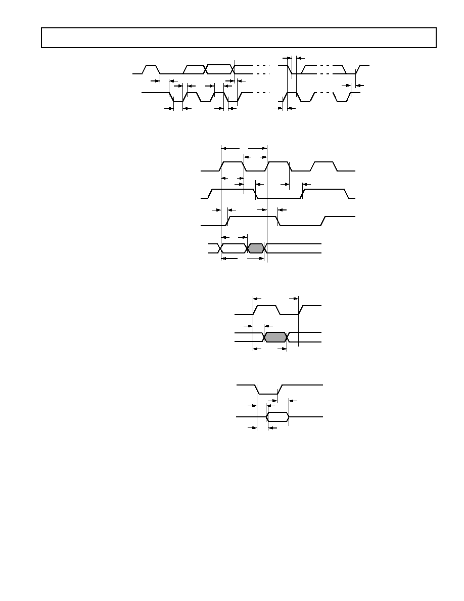
5
SDATA
SCLOCK
t
3
t
2
t
6
t
1
t
7
t
5
t
4
t
3
t
8
Figure 1. MPU Port Timing Diagram
LLC1
LLCREF
LLC2
OUTPUTS P0P19, HREF, VREF,
VSYNC, HSYNC, FIELD, DV
t
12
t
14
t
11
t
10
t
9
t
15
t
16
t
17
t
13
Figure 2. LLC Clock, Pixel Port, and Control Outputs Timing Diagram
CLKIN
OUTPUTS P0P19, HREF, VREF,
VSYNC, HSYNC, FIELD, DV
t
18
t
19
t
20
Figure 3. Pixel Port and Control Outputs in CAPI and SCAPI Mode Timing Diagram
OE
OUTPUTS P0P19, HS, VS, VREF,
HREF, FIELD, DV
t
23
t
21
t
22
Figure 4.
OE Timing Diagram