ADV7188 Multiformat SDTV Video Decoder with Fast Switch Overlay Support Data Sheet (Rev. 0)

Multiformat SDTV Video Decoder with Fast
Switch Overlay Support
ADV7188
Rev. 0
Information furnished by Analog Devices is believed to be accurate and reliable.
However, no responsibility is assumed by Analog Devices for its use, nor for any
infringements of patents or other rights of third parties that may result from its use.
Specifications subject to change without notice. No license is granted by implication
or otherwise under any patent or patent rights of Analog Devices. Trademarks and
registered trademarks are the property of their respective owners.
One Technology Way, P.O. Box 9106, Norwood, MA 02062-9106, U.S.A.
Tel: 781.329.4700
www.analog.com
Fax: 781.461.3113
© 2005 Analog Devices, Inc. All rights reserved.
FEATURES
Multiformat video decoder supports NTSC-(J, M, 4.43),
PAL-(B/D/G/H/I/M/N), SECAM
Integrates four 54 MHz, Noise Shaped Video®, 12-bit ADCs
SCART fast blank support
Clocked from a single 28.63636 MHz crystal
Line-locked clock-compatible (LLC)
Adaptive digital line length tracking (ADLLTTM), signal
processing, and enhanced FIFO management give mini
TBC functionality
5-line adaptive comb filters
Proprietary architecture for locking to weak, noisy, and
unstable video sources such as VCRs and tuners
Subcarrier frequency lock and status information output
Integrated AGC with adaptive peak white mode
Macrovision® copy protection detection
CTI (chroma transient improvement)
DNR (digital noise reduction)
Multiple programmable analog input formats
CVBS (composite video)
S-Video (Y/C)
YPrPb component (VESA, MII, SMPTE, and Betacam)
12 analog video input channels
Integrated anti-aliasing filters
Programmable Interrupt request output pin
Automatic NTSC/PAL/SECAM identification
Digital output formats (8-bit, 10-bit, 16-bit, or 20-bit)
ITU-R BT.656 YCrCb 4:2:2 output + HS, VS, and FIELD
0.5 V to 1.6 V analog signal input range
Differential gain: 0.4% typ
Differential phase: 0.4° typ
Programmable video controls
Peak white/hue/brightness/saturation/contrast
Integrated on-chip video timing generator
Free-run mode (generates stable video output with no I/P)
VBI decode support for close captioning (including XDS),
WSS, CGMS, Gemstar® 1×/2×, teletext, VITC, VPS
Power-down mode
2-wire serial MPU interface (I
2
C®-compatible)
3.3 V analog, 1.8 V digital core; 3.3 V IO supply
Industrial temperature grade: 40°C to +85°C
80-lead LQFP Pb-free package
APPLICATIONS
High end DVD recorders
Video projectors
HDD-based PVRs/DVDRs
LCD TVs
Set-top boxes
Professional video products
AVR receiver
GENERAL DESCRIPTION
The ADV7188 integrated video decoder automatically detects
and converts a standard analog baseband television signal that
is compatible with worldwide standards NTSC, PAL, and
SECAM, into 4:2:2 component video data-compatible with 20-,
16-, 10-, and 8-bit CCIR601/CCIR656.
The advanced and highly flexible digital output interface enables
performance video decoding and conversion in line-locked
clock-based systems. This makes the device ideally suited for a
broad range of applications with diverse analog video character-
istics, including tape-based sources, broadcast sources,
security/surveillance cameras, and professional systems.
The 12-bit accurate ADC provides professional quality video
performance and is unmatched. This allows true 10-bit
resolution in the 10-bit output mode.
The 12 analog input channels accept standard composite,
S-Video, and YPrPb video signals in an extensive number of
combinations.
AGC and clamp restore circuitry allow an input video signal
peak-to-peak range of 0.5 V to 1.6 V. Alternatively, these can be
bypassed for manual settings.
The fixed 54 MHz clocking of the ADCs and datapath for all
modes allows very precise, accurate sampling and digital
filtering. The line-locked clock output allows the output data
rate, timing signals, and output clock signals to be synchronous,
asynchronous, or line locked even with ±5% line length variation.
The output control signals allow glueless interface connections
in almost any application. The ADV7188 modes are set up over
a 2-wire, serial, bidirectional port (I
2
C-compatible).
SCART and overlay functionality are enabled by the ADV7188's
ability to simultaneously process CVBS and standard definition
RGB signals. Signal mixing is controlled by the fast blank pin.
The ADV7188 is fabricated in a 3.3 V CMOS process. Its
monolithic CMOS construction ensures greater functionality
with lower power dissipation. It is packaged in a small 80-lead
LQFP Pb-free package.

ADV7188
Rev. 0 | Page 2 of 112
TABLE OF CONTENTS
Introduction ...................................................................................... 4
Analog Front End ......................................................................... 4
Standard Definition Processor (SDP)........................................ 4
Electrical Characteristics............................................................. 5
Video Specifications..................................................................... 6
Timing Specifications .................................................................. 7
Analog Specifications................................................................... 7
Thermal Specifications ................................................................ 8
Timing Diagrams.......................................................................... 8
Absolute Maximum Ratings............................................................ 9
Package Thermal Performance................................................... 9
ESD Caution.................................................................................. 9
Pin Configuration and Function Descriptions........................... 10
Analog Front End ........................................................................... 12
Analog Input Muxing ................................................................ 12
Manual Input Muxing................................................................ 14
XTAL Clock Input Pin Functionality....................................... 15
28.63636 MHz Crystal Operation ............................................ 15
Antialiasing Filters ..................................................................... 15
SCART and Fast Blanking......................................................... 15
Fast Blank Control...................................................................... 16
Readback of FB Pin Status......................................................... 18
Global Control Registers ............................................................... 19
Power-Save Modes...................................................................... 19
Reset Control .............................................................................. 19
Global Pin Control ..................................................................... 19
Global Status Registers................................................................... 21
Standard Definition Processor (SDP).......................................... 22
SD Luma Path ............................................................................. 22
SD Chroma Path......................................................................... 22
Sync Processing........................................................................... 23
VBI Data Recovery..................................................................... 23
General Setup.............................................................................. 23
Color Controls ............................................................................ 25
Clamp Operation........................................................................ 27
Luma Filter .................................................................................. 28
Chroma Filter.............................................................................. 31
Gain Operation........................................................................... 32
Chroma Transient Improvement (CTI) .................................. 35
Digital Noise Reduction (DNR), and Luma Peaking Filter .. 36
Comb Filters................................................................................ 37
AV Code Insertion and Controls ............................................. 39
Synchronization Output Signals............................................... 41
Sync Processing .......................................................................... 48
VBI Data Decode ....................................................................... 49
I
2
C Readback Registers .............................................................. 58
Pixel Port Configuration ............................................................... 72
MPU Port Description................................................................... 73
Register Accesses ........................................................................ 74
Register Programming............................................................... 74
I
2
C Sequencer.............................................................................. 74
I
2
C Register Maps ........................................................................... 75
User Map ..................................................................................... 75
User Sub Map.............................................................................. 91
I
2
C Programming Examples........................................................ 100
Mode 1 CVBS Input................................................................. 100
Mode 2 S-Video Input ............................................................. 101
Mode 3 525i/625i YPrPb Input .............................................. 102
Mode 4 SCART--S-Video or CVBS autodetect ................... 103
Mode 5 SCART Fast Blank--CVBS & RGB ......................... 104
Mode 6 SCART RGB Input (Static Fast Blank)--CVBS and
RGB ............................................................................................ 105
PCB Layout Recommendations.................................................. 106

ADV7188
Rev. 0 | Page 3 of 112
Analog Interface Inputs........................................................... 106
Power Supply Decoupling ....................................................... 106
PLL ............................................................................................. 106
Digital Outputs (Both Data and Clocks) .............................. 106
Digital Inputs ............................................................................ 107
XTAL And Load Capacitor Values Selection ........................107
Typical Circuit Connection .........................................................108
Outline Dimensions......................................................................109
Ordering Guide .........................................................................109
REVISION HISTORY
7/05--Revision 0: Initial Version
ADV7188
Rev. 0 | Page 4 of 112
INTRODUCTION
The ADV7188 is a high quality, single chip, multiformat video
decoder that automatically detects and converts PAL, NTSC,
and SECAM standards in the form of composite, S-Video, and
component video into a digital ITU-R BT.656 format.
The advanced and highly flexible digital output interface enables
performance video decoding and conversion in line-locked
clock-based systems. This makes the device ideally suited for a
broad range of applications with diverse analog video
characteristics, including tape-based sources, broadcast sources,
security and surveillance cameras, and professional systems.
ANALOG FRONT END
The ADV7188 analog front end includes four 12-bit noise
shaped video ADCs that digitize the analog video signal before
applying it to the standard definition processor. The analog
front end uses differential channels to each ADC to ensure high
performance in mixed-signal applications.
The front end also includes a 12-channel input mux that enables
multiple video signals to be applied to the ADV7188. Current
and voltage clamps are positioned in front of each ADC to
ensure that the video signal remains within the range of the
converter. Fine clamping of the video signals is performed
downstream by digital fine clamping within the ADV7188. The
ADCs are configured to run in 4× oversampling mode.
The ADV7188 has optional anti-aliasing filters on each of the
four input channels. The filters are designed for SD video with
approximately 6 MHz bandwidth.
SCART and overlay functionality are enabled by the ADV7188's
ability to simultaneously process CVBS and Standard Definition
RGB signals. Signal mixing is controlled by the Fast Blank pin.
STANDARD DEFINITION PROCESSOR (SDP)
The ADV7188 is capable of decoding a large selection of
baseband video signals in composite, S-Video, and component
formats. The video standards supported include PAL
B/D/I/G/H, PAL60, PAL M, PAL N, PAL Nc, NTSC M/J, NTSC
4.43, and SECAM B/D/G/K/L. The ADV7188 can automatically
detect the video standard and process it accordingly.
The ADV7188 has a 5-line, superadaptive, 2D comb filter that
gives superior chrominance and luminance separation when
decoding a composite video signal. This highly adaptive filter
automatically adjusts its processing mode according to video
standard and signal quality without user intervention. Video
user controls such as brightness, contrast, saturation, and hue
are also available within the ADV7188.
The ADV7188 implements a patented adaptive digital line
length tracking (ADLLT) algorithm to track varying video line
lengths from sources such as a VCR. ADLLT enables the
ADV7188 to track and decode poor quality video sources such
as VCRs, noisy sources from tuner outputs, VCD players, and
camcorders. The ADV7188 contains a chroma transient
improvement (CTI) processor that sharpens the edge rate of
chroma transitions, resulting in sharper vertical transitions.
The ADV7188 can process a variety of VBI data services, such
as closed captioning (CC), wide screen signaling (WSS), copy
generation management system (CGMS), Gemstar 1×/2×,
extended data service (XDS) and teletext. The ADV7188 is fully
Macrovision certified; detection circuitry enables Type I, II, and
III protection levels to be identified and reported to the user.
The decoder is also fully robust to all Macrovision signal inputs.
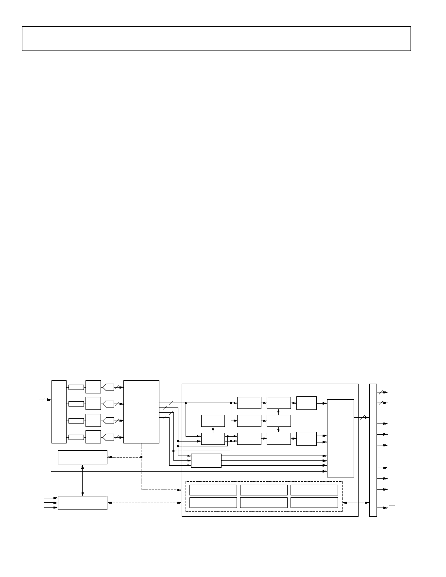
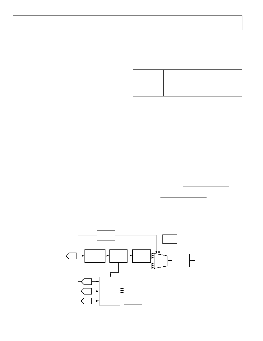
FUNCTIONAL BLOCK DIAGRAM
CVBS
S-VIDEO
YPrPb
RGB + CVBS
A/D
ANTI
ALIAS
FILTER
12
A/D
ANTI
ALIAS
FILTER
12
A/D
ANTI
ALIAS
FILTER
12
A/D
ANTI
ALIAS
FILTER
12
AIN1
AIN12
12
INPUT
MUX
DATA
PREPROCESSOR
LUMA
FILTER
SYNC
EXTRACT
CHROMA
FILTER
LUMA
RESAMPLE
RESAMPLE
CONTROL
F
SC
RECOVERY
CHROMA
RESAMPLE
CHROMA
DEMOD
COLORSPACE
CONVERSION
LUMA
2D COMB
(5H MAX)
CHROMA
2D COMB
(4H MAX)
CVBS
DECIMATION AND
DOWNSAMPLING
FILTERS
12
12
12
12
Cr
Y
Cb
CLAMP
CLAMP
CLAMP
CLAMP
FAST BLANK
OVERLAY
CONTROL
VBI DATA RECOVERY
MACROVISION
DETECTION
GLOBAL CONTROL
STANDARD
AUTODETECTION
SYNTHESIZED
LLC CONTROL
FREE RUN
OUTPUT CONTROL
20
STANDARD DEFINITION PROCESSOR
R
G
B
Cr
Cb
C
10
10
PIXEL
DATA
P19-P10
P9-P0
HS
SFL
LLC2
LLC1
FIELD
VS
INT
OUTPUT FORM
ATTER
CONTROL
AND DATA
FB
SYNC PROCESSING AND
CLOCK GENERATION
SERIAL INTERFACE
CONTROL AND VBI DATA
SYNC AND
CLK CONTROL
ADV7188
05478-001
Y
Cr
Cb
CVBS/Y
SCLK
SDA
ALSB
Figure 1.

ADV7188
Rev. 0 | Page 5 of 112
ELECTRICAL CHARACTERISTICS
At A
VDD
= 3.15 V to 3.45 V, D
VDD
= 1.65 V to 2.0 V, D
VDDIO
= 3.0 V to 3.6 V, P
VDD
= 1.71 V to 1.89 V, nominal input range 1.6 V.
Operating temperature range, unless otherwise noted.
Table 1.
Parameter Symbol
Test
Conditions
Min
Typ
Max
Unit
STATIC PERFORMANCE
1, 2, 3
Resolution (Each ADC)
N
12
Bits
Integral Nonlinearity
INL
BSL at 54 MHz
1.5/+2.5
±8
LSB
Differential Nonlinearity
DNL
BSL at 54 MHz
0.7/+0.7
0.99/+2.5
LSB
DIGITAL INPUTS
Input High Voltage
4
V
IH
2
V
Input Low Voltage
5
V
IL
0.8 V
Input Current
I
IN
Pins listed in Note 6 50
+50 A
All other pins
7
10
+10
A
Input Capacitance
9
C
IN
10 pF
DIGITAL OUTPUTS
Output High Voltage
8
V
OH
I
SOURCE
= 0.4 mA
2.4
V
Output Low Voltage
8
V
OL
I
SINK
= 3.2 mA
0.4
V
High Impedance Leakage Current
I
LEAK
10 A
Output Capacitance
9
C
OUT
20
pF
POWER REQUIREMENTS
9
Digital Core Power Supply
D
VDD
1.65
1.8
2.0
V
Digital I/O Power Supply
D
VDDIO
3.0
3.3
3.6
V
PLL Power Supply
P
VDD
1.71
1.8
1.89 V
Analog Power Supply
A
VDD
3.15
3.3
3.45 V
Digital Core Supply Current
I
DVDD
105
mA
Digital I/O Supply Current
I
DVDDIO
4
mA
PLL Supply Current
I
PVDD
11
mA
Analog Supply Current
I
AVDD
CVBS
input
10
99
mA
SCART RGB FB input
11
269
mA
Power-Down Current
I
PWRDN
0.65
mA
Power-Up Time
t
PWRUP
20
ms
1
All ADC linearity tests performed at input range of full scale 12.5%, and at zero scale +12.5%.
2
Max INL and DNL specificationss obtained with part configured for component video input.
3
Temperature range T
MIN
to T
MAX
, 40°C to +85°C. The min/max specifications are guaranteed over this range.
4
To obtain specified V
IH
level on Pin 29, register 0x13 (write only) must be programmed with value 0x04. If Register 0x13 is programmed with value 0x00, then V
IH
on Pin 29 = 1.2 V.
5
To obtain specified V
IL
level on Pin 29, register 0x13 (write only) must be programmed with value 0x04. If Register 0x13 is programmed with value 0x00, then V
IL
on Pin 29 = 0.4 V.
6
Pins: 36, 64, 79.
7
Excluding all "TEST" pins (TEST0 to TEST8)
8
V
OH
and V
OL
levels obtained using default drive strength value (0xD5) in register subaddress 0xF4.
9
Guaranteed by characterization.
10
ADC0 powered on only.
11
All four ADCs powered on.

ADV7188
Rev. 0 | Page 6 of 112
VIDEO SPECIFICATIONS
At A
VDD
= 3.15 V to 3.45 V, D
VDD
= 1.65 V to 2.0 V, D
VDDIO
= 3.0 V to 3.6 V, P
VDD
= 1.71 V to 1.89 V (operating temperature range, unless
otherwise noted).
Table 2.
Parameter
1, 2
Symbol
Test
Conditions
Min
Typ
Max
Unit
NONLINEAR SPECIFICATIONS
Differential Phase
DP
CVBS I/P, modulate 5-step
0.4
0.6
degree
Differential Gain
DG
CVBS I/P, modulate 5-step
0.4
0.6
%
Luma Nonlinearity
LNL
CVBS I/P, 5-step
0.4
0.7
%
NOISE SPECIFICATIONS
SNR Unweighted
Luma ramp
61
63
dB
Luma flat field
63
65
dB
Analog Front End Crosstalk
60
dB
LOCK TIME SPECIFICATIONS
Horizontal Lock Range
5
+5
%
Vertical Lock Range
40
70
Hz
Fsc Subcarrier Lock Range
±1.3
Hz
Color Lock In Time
60
Lines
Sync Depth Range
3
20
200
%
Color Burst Range
5
200
%
Vertical Lock Time
2
Fields
Autodetection Switch Speed
100
Lines
CHROMA SPECIFICATIONS
Hue Accuracy
HUE
1
degree
Color Saturation Accuracy
CL_AC
1
%
Color AGC Range
5
400
%
Chroma Amplitude Error
0.4
%
Chroma Phase Error
0.3
degree
Chroma Luma Intermodulation
0.1
%
LUMA SPECIFICATIONS
Luma Brightness Accuracy
CVBS, 1 V I/P
1
%
Luma Contrast Accuracy
CVBS, 1 V I/P
1
%
1
Temperature range T
MIN
to T
MAX
, 40°C to +85°C. The min/max specifications are guaranteed over this range.
2
Guaranteed by characterization.
3
Nominal sync depth is 300 mV at 100% sync depth range.

ADV7188
Rev. 0 | Page 7 of 112
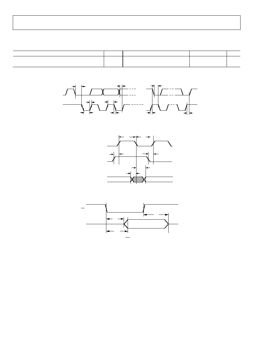
TIMING SPECIFICATIONS
At A
VDD
= 3.15 V to 3.45 V, D
VDD
= 1.65 V to 2.0 V, D
VDDIO
= 3.0 V to 3.6 V, P
VDD
= 1.71 V to 1.89 V (operating temperature range, unless
otherwise noted).
Table 3.
Parameter
1, 2
Symbol
Test
Conditions
Min
Typ
Max
Unit
SYSTEM CLOCK AND CRYSTAL
Nominal Frequency
28.63636
MHz
Frequency Stability
±50
ppm
I
2
C PORT
3
SCLK Frequency
400
kHz
SCLK Min Pulse Width High
t
1
0.6
s
SCLK Min Pulse Width Low
t
2
1.3
s
Hold Time (Start Condition)
t
3
0.6
s
Setup Time (Start Condition)
t
4
0.6
s
SDA Setup Time
t
5
100
ns
SCLK and SDA Rise Time
t
6
300
ns
SCLK and SDA Fall Time
t
7
300
ns
Setup Time for Stop Condition
t
8
0.6 s
RESET
FEATURE
Reset Pulse Width
5
ms
CLOCK
OUTPUTS
LLC1 Mark Space Ratio
t
9
:t
10
45:55
55:45 %
Duty
Cycle
LLC1 Rising to LLC2 Rising
t
11
1
ns
LLC1 Rising to LLC2 Falling
t
12
1
ns
DATA AND CONTROL OUTPUTS
Data Output Transitional Time
4
t
13
Negative clock edge to start of valid data
(t
ACCESS
= t
10
t
13
)
3.6
ns
Data Output Transitional Time
4
t
14
End of valid data to negative clock edge
(t
HOLD
= t
9
+ t
14
)
2.4
ns
Propagation Delay to Hi Z
t
15
6
ns
Max Output Enable Access Time
t
16
7
ns
Min Output Enable Access Time
t
17
4
ns
1
Temperature range T
MIN
to T
MAX
, 40°C to +85°C. The min/max specifications are guaranteed over this range.
2
Guaranteed by characterization.
3
TTL input values are 0 to 3 volts, with rise/fall times
3 ns, measured between the 10% and 90% points.
4
SDP timing figures obtained using default drive strength value (0xD5) in register subaddress 0xF4.
ANALOG SPECIFICATIONS
At A
VDD
= 3.15 V to 3.45 V, D
VDD
= 1.65 V to 2.0 V, D
VDDIO
= 3.0 V to 3.6 V, P
VDD
= 1.71 V to 1.89 V (operating temperature range, unless
otherwise noted). Recommended analog input video signal range: 0.5 V to 1.6 V, typically 1 V p-p.
Table 4.
Parameter
1, 2
Symbol
Test
Condition
Min
Typ
Max
Unit
CLAMP CIRCUITRY
External Clamp Capacitor
0.1
F
Input Impedance
3
Clamps switched off
10
M
Input impedance of Pin 40 (FB)
20
k
Large Clamp Source Current
0.75
mA
Large Clamp Sink Current
0.75
mA
Fine Clamp Source Current
60
A
Fine Clamp Sink Current
60
A
1
Temperature range T
MIN
to T
MAX
, 40°C to +85°C. The min/max specifications are guaranteed over this range.
2
Guaranteed by characterization.
3
Except Pin 40 (FB).
ADV7188
Rev. 0 | Page 8 of 112
THERMAL SPECIFICATIONS
Table 5.
Parameter Symbol
Test
Conditions
Min
Typ
Max
Unit
Junction-to-Case Thermal Resistance
JC
4-layer PCB with solid ground plane
7.6
°C/W
Junction-to-Ambient Thermal Resistance (Still Air)
JA
4-layer PCB with solid ground plane
38.1
°C/W
TIMING DIAGRAMS
05478-002
SDA
SCLK
t
3
t
5
t
3
t
4
t
8
t
6
t
7
t
2
t
1
Figure 2. I
2
C Timing
OUTPUT LLC 1
OUTPUT LLC 2
05478-003
OUTPUTS P0P19, VS,
HS, FIELD,
SFL
t
9
t
11
t
10
t
14
t
13
t
12
Figure 3. Pixel Port and Control Output Timing
05478-004
OE
P0P19, HS,
VS, FIELD,
SFL
t
15
t
16
t
17
Figure 4. OE Timing

ADV7188
Rev. 0 | Page 9 of 112
ABSOLUTE MAXIMUM RATINGS
Table 6.
Parameter Rating
A
VDD
to AGND
4 V
D
VDD
to DGND
2.2 V
P
VDD
to AGND
2.2 V
D
VDDIO
to DGND
4 V
D
VDDIO
to AVDD
0.3 V to +0.3 V
P
VDD
to D
VDD
0.3 V to +0.3 V
D
VDDIO
to P
VDD
0.3V to +2 V
D
VDDIO
to D
VDD
0.3V to +2 V
A
VDD
to P
VDD
0.3V to +2 V
A
VDD
to D
VDD
0.3V to +2 V
Digital Inputs Voltage to DGND
0.3V to D
VDDIO
+ 0.3 V
Digital Output Voltage to DGND
0.3V to D
VDDIO
+ 0.3 V
Analog Inputs to AGND
AGND 0.3 V to A
VDD
+ 0.3 V
Maximum Junction Temperature
(T
J
max)
125°C
Storage Temperature Range
65°C to +150°C
Infrared Reflow Soldering (20 sec)
260°C
Stresses above those listed under Absolute Maximum Ratings
may cause permanent damage to the device. This is a stress
rating only; functional operation of the device at these or any
other conditions above those indicated in the operational
section of this specification is not implied. Exposure to absolute
maximum rating conditions for extended periods may affect
device reliability.
PACKAGE THERMAL PERFORMANCE
To reduce power consumption the user is advised to turn off
any unused ADCs when using the part.
The junction temperature must always stay below the
maximum junction temperature (T
J
max) of 125°C. The
following equation shows how to calculate the junction
temperature:
T
J
= T
A Max
+ (
JA
× W
Max
)
where:
T
A Max
= 85°C.
JA
= 30°C/W.
W
Max
= ((A
VDD
× I
AVDD
) + ( D
VDD
× I
DVDD
) + (D
VDDIO
× I
DVDDIO
) +
(P
VDD
× I
PVDD
)).
ESD CAUTION
ESD (electrostatic discharge) sensitive device. Electrostatic charges as high as 4000 V readily accumulate on
the human body and test equipment and can discharge without detection. Although this product features
proprietary ESD protection circuitry, permanent damage may occur on devices subjected to high energy
electrostatic discharges. Therefore, proper ESD precautions are recommended to avoid performance
degradation or loss of functionality.
ADV7188
Rev. 0 | Page 10 of 112
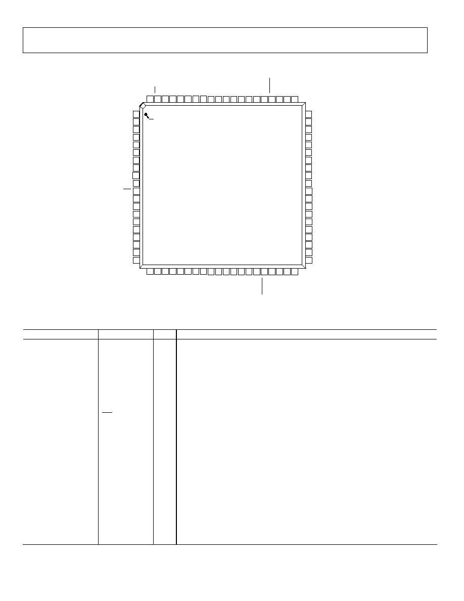
PIN CONFIGURATION AND FUNCTION DESCRIPTIONS
2
HS
3
DGND
4
DVDDIO
7
P13
6
P14
5
P15
1
VS
8
P12
9
DGND
10
DVDD
12
SFL
13
TEST2
14
DGND
15
DVDDIO
16
TEST8
17
P11
18
P10
19
P9
20
P8
11
INT
59
58
57
54
55
56
60
53
52
AIN11
AIN4
AIN10
CAPC1
CAPC2
AGND
AIN5
AGND
CML
51
REFOUT
49
CAPY2
48
CAPY1
47
AGND
46
AIN3
45
AIN9
44
AIN2
43
AIN8
42
AIN1
41
AIN7
50
AVDD
21
P7
22
P6
23
P5
24
P4
25
TEST3
26
LLC2
27
LLC1
28
XTA
L
1
29
XTA
L
30
DV
DD
31
DGND
32
P3
33
P2
34
P1
35
P0
36
P
W
RDN
37
ELPF
38
PVD
D
39
AGND
40
FB
80
FIELD
79
OE
78
TEST1
77
TEST6
76
P16
75
P17
74
P18
73
P19
72
DV
DD
71
DGND
70
TEST0
69
TEST4
68
SC
LK
67
SD
A
66
ALS
B
65
TEST7
64
R
ESET
63
TEST5
62
AIN6
61
AIN1
2
PIN 1
ADV7188
TOP VIEW
(Not to Scale)
05478-005
Figure 5. 80-Lead LQFP Pin Configuration
Table 7. Pin Function Descriptions
Pin No.
Mnemonic
Type
Function
3, 9, 14, 31, 71
DGND
G
Digital Ground.
39, 47, 53, 56
AGND
G
Analog Ground.
4, 15
DVDDIO
P
Digital I/O Supply Voltage (3.3 V).
10, 30, 72
DVDD
P
Digital Core Supply Voltage (1.8 V).
50
AVDD
P
Analog Supply Voltage (3.3 V).
38
PVDD
P
PLL Supply Voltage (1.8 V).
42, 44, 46, 58, 60, 62,
41, 43, 45, 57, 59, 61
AIN1 to AIN12
I
Analog Video Input Channels.
11
INT
O
Interrupt Request Output. Interrupt occurs when certain signals are detected on the
input video. See the User Sub Map register details in Table 103.
40 FB
I
Fast Blank. FB is a fast switch overlay input that switches between CVBS and RGB analog
signals.
70, 78, 13, 25, 69, 63
TEST0 to TEST5
Leave these pins unconnected.
77, 65
TEST6 to TEST7
Tie to AGND
16
TEST8
Tie to DVDDIO
35, 34, 33, 32, 24, 23,
22, 21, 20, 19, 18, 17, 8,
7, 6, 5, 76, 75, 74, 73
P0 to P19
O
Video Pixel Output Port.
2
HS
O
Horizontal Synchronization Output Signal.
1
VS
O
Vertical Synchronization Output Signal.
80
FIELD
O
Field Synchronization Output Signal.
67 SDA
I/O
I
2
C Port Serial Data Input/Output Pin.
68 SCLK
I
I
2
C Port Serial Clock Input (Max Clock Rate of 400 kHz).

ADV7188
Rev. 0 | Page 11 of 112
Pin No.
Mnemonic
Type
Function
66 ALSB
I
This pin selects the I
2
C address for the ADV7188. ALSB set to Logic 0 sets the address for a
write as 0x40; set to Logic 1 sets the address to 0x42.
64
RESET
I
System Reset Input, Active Low. A minimum low reset pulse width of 5 ms is required to
reset the ADV7188 circuitry.
27
LLC1
O
Line-Locked Clock 1. This is a line-locked output clock for the pixel data output by the
ADV7188. Nominally 27 MHz, but varies up or down according to video line length.
26
LLC2
O
Line-Locked Clock 2. This is a divide-by-2 version of the LLC1 output clock for the pixel
data output by the ADV7188. Nominally 13.5 MHz, but varies up or down according to
video line length.
29
XTAL
I
This is the input pin for the 28.63636 MHz crystal, or can be overdriven by an external 3.3
V, 28.63636 MHz clock oscillator source. In crystal mode, the crystal must be a
fundamental crystal.
28
XTAL1
O
This pin should be connected to the 28.63636 MHz crystal or left as a no connect if an
external 3.3 V, 28.63636 MHz clock oscillator source is used to clock the ADV7188. In
crystal mode, the crystal must be a fundamental crystal.
36
PWRDN
I
Logic 0 on this pin places the ADV7188 in a power-down mode. Refer to the I
2
C Register
Maps section for more options on power-down modes for the ADV7188.
79
OE
I
When set to Logic 0, OE enables the pixel output bus, P19 to P0 of the ADV7188. Logic 1
on the OE pin places P19 to P0, HS, VS, and SFL/SYNC_OUT into a high impedance state.
37
ELPF
I
The recommended external loop filter must be connected to this ELPF pin, as shown in
Figure 50.
12
SFL
O
Subcarrier Frequency Lock. This pin contains a serial output stream that can be used to
lock the subcarrier frequency when this decoder is connected to any Analog Devices, Inc.
digital video encoder.
51
REFOUT
O
Internal Voltage Reference Output. Refer to Figure 50 for a recommended capacitor
network for this pin.
52 CML
O
The CML pin is a common-mode level for the internal ADC's. Refer to Figure 50 for a
recommended capacitor network for this pin.
48, 49
CAPY1, CAPY2
I
ADC's Capacitor Network. Refer to Figure 50 for a recommended capacitor network for
this pin.
54. 55
CAPC1, CAPC2
I
ADC's Capacitor Network. Refer to Figure 50 for a recommended capacitor network for
this pin.
ADV7188
Rev. 0 | Page 12 of 112
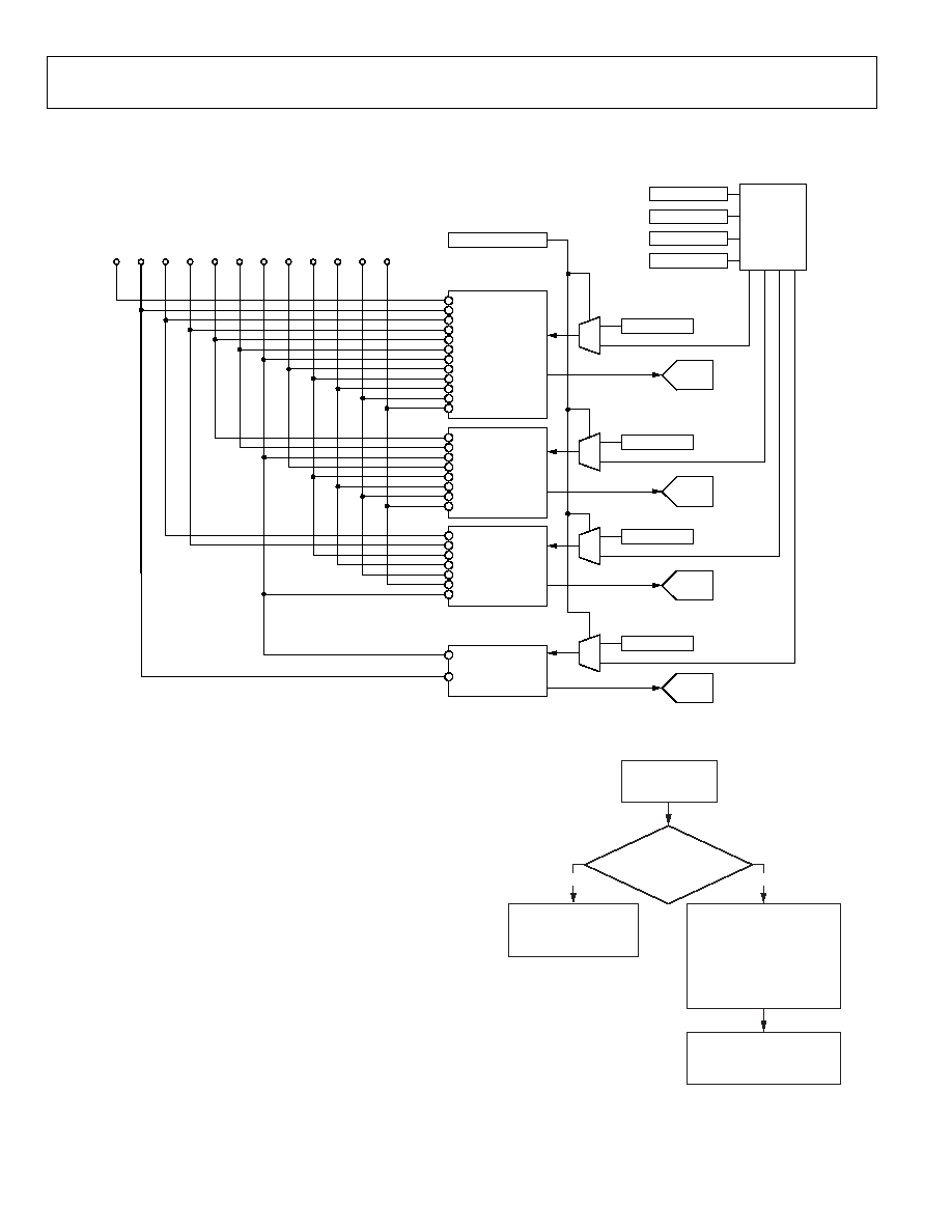
ANALOG FRONT END
ANALOG INPUT MUXING
AIN1
AIN7
AIN2
AIN8
AIN3
AIN9
AIN4
AIN10
AIN5
AIN11
AIN6
AIN12
AIN3
AIN4
AIN2
AIN9
AIN7
AIN8
AIN4
AIN5
AIN10
AIN11
AIN5
AIN6
AIN11
AIN6
AIN4
AIN12
AIN12
AIN1
AIN7
AIN2
AIN8
AIN3
AIN9
AIN4
AIN1
0
AIN5
AIN1
1
AIN6
AIN1
2
1
0
ADC2_SW[3:0]
ADC2
1
0
ADC3_SW[3:0]
ADC3
1
0
ADC1_SW[3:0]
ADC1
1
0
ADC0_SW[3:0]
ADC0
ADC_SW_MAN_EN
SDM_SEL[1:0]
PRIM_MODE[3:0]
INSEL[3:0]
RGB_IP_SEL
INTERNAL
MAPPING
FUNCTIONS
05478-006
Figure 6. Internal Pin Connections
The ADV7188 has an integrated analog muxing section that
allows connecting more than one source of video signal to the
decoder. Figure 6 outlines the overall structure of the input
muxing provided in ADV7188.
As can be seen in Figure 6, the analog input muxes can be
controlled in two ways:
·
By functional registers (INSEL). Using INSEL[3:0]
simplifies the setup of the muxes, and minimizes crosstalk
between channels by pre-assigning the input channels. This
is referred to as ADI recommended input muxing.
·
By an I
2
C manual override (ADC_SW_MAN_EN,
ADC0_SW, ADC1_SW, ADC2_SW, and ADC3_SW). This
is provided for applications with special requirements, such
as number/combinations of signals, which would not be
served by the pre-assigned input connections. This is
referred to as manual input muxing.
Refer to Figure 7 for an overview of the two methods of
controlling input muxing.
05478-007
SET INSEL[3:0] TO
CONFIGURE ADV7188
TO DECODE VIDEO FORMAT:
CVBS: 0000
YC: 0110
YPrPb: 1001
SCART (CVBS/RGB): 1111
SET SDM_SEL[1:0] FOR
S-VIDEO/CVBS AUTODETECT
USE MANUAL INPUT MUXING
(ADC_SW_MAN_EN, ADC0_SW,
ADC1_SW, ADC2_SW,
ADC3_SW)
SET INSEL[3:0] AND
SDM_SEL[1:0]
FOR REQUIRED MUXING
CONFIGURATION
CONNECTING
ANALOG SIGNALS
TO ADV7188
ADI RECOMMENDED
INPUT MUXING;
SEE TABLES 8 AND 9
NO
YES
Figure 7. Input Muxing Overview

ADV7188
Rev. 0 | Page 13 of 112
ADI Recommended Input Muxing
A maximum of 12 CVBS inputs can be connected and decoded
by the ADV7188. As seen in Figure 5, this means the sources
must be connected to adjacent pins on the IC. This calls for a
careful design of the PCB layout, for example, ground shielding
between all signals routed through tracks that are physically
close together.
SDM_SEL[1:0], S-Video and CVBS Autodetect Mode Select,
Address 0x69 [1:0]
The SDM_SEL bits decide on input routing and whether
INSEL[3:0] is used to govern I/P routing decisions.
The CVBS/YC autodetection feature is enabled using
SDM_SEL = 11.
Table 8: SDM_SEL[1:0]
SDM_SEL[1:0]
Mode
Analogue Video Inputs
00
As per INSEL[3:0]
As per INSEL[3:0]
01 CVBS AIN11
10 YC Y = AIN10
C = AIN12
11 YC/CVBS
auto
CVBS = AIN11
Y = AIN11
C = AIN12
INSEL[3:0] Input Selection, Address 0x00 [3:0]
The INSEL bits allow the user to select an input channel and the
input format. Depending on the PCB connections, only a subset
of the INSEL modes are valid. The INSEL[3:0] not only switches
the analog input muxing, it also configures ADV7188 to process
CVBS (Comp), S-Video (Y/C), or component (YPbPr) format.
ADI-recommended input muxing is designed to minimize
crosstalk between signal channels and to obtain the highest
level of signal integrity. Table 10 summarizes how the PCB
layout should connect analog video signals to the ADV7188.
It is strongly recommended to connect any unused analog input
pins to AGND to act as a shield.
Connect inputs AIN7 to AIN11 to AGND when only six input
channels are used. This improves the quality of the sampling
due to better isolation between the channels.
AIN12 is not under the control of INSEL[3:0]. It can be routed
to ADC0/ADC1/ADC2 only by manual muxing. See Table 11
for details.
Table 9. Input Channel Switching Using INSEL[3:0]
Description
INSEL[3:0]
Analog Input Pins
Video Format
0000(default)
CVBS1 = AIN1
B = AIN4 or AIN7
1
R = AIN5 or AIN8
1
G = AIN6 or AIN9
1
SCART (CVBS and R, G, B )
0001
CVBS2 = AIN2
B = AIN4 or AIN7
1
R = AIN5 or AIN8
1
G = AIN6 or AIN9
1
SCART (CVBS and R, G, B )
0010
CVBS3 = AIN3
B = AIN4 or AIN7
1
R = AIN5 or AIN8
1
G = AIN6 or AIN9
1
SCART (CVBS and R, G, B )
0011
CVBS4 = AIN4
B = AIN7
R = AIN8
G = AIN9
SCART (CVBS and R, G, B )
0100
CVBS1 = AIN1
B = AIN4
R = AIN5
G = AIN6
SCART (CVBS and R, G, B )
0101
CVBS1 = AIN1
B = AIN4
R = AIN5
G = AIN6
SCART (CVBS and R, G, B )
0110
Y1 = AIN1
C1 = AIN4
YC
0111
Y2 = AIN2
C2 = AIN5
YC
Description
INSEL[3:0]
Analog Input Pins
Video Format
1000
Y3 = AIN3
C3 = AIN6
YC
1001
Y1 = AIN1
PB1 = AIN4
PR1 = AIN5
YPrPb
1010
Y2 = AIN2
PB2 = AIN3
PR2 = AIN6
YPrPb
1011
CVBS7 = AIN7
B = AIN7
R = AIN8
G = AIN9
SCART (CVBS and R, G, B )
1100
CVBS8 = AIN8
B = AIN7
R = AIN8
G = Ain9
SCART (CVBS and R, G, B )
1101
CVBS9 = AIN9
B = AIN7
R = AIN8
G = Ain9
SCART (CVBS and R, G, B )
1110
CVBS10 = AIN10
B = AIN4 or AIN7
1
R = Ain5 or Ain8
1
G = Ain6 or Ain9
1
SCART (CVBS and R, G, B )
1111
CVBS11 = AIN11
B = AIN4 or AIN7
1
R = AIN5 or AIN8
1
G = AIN6 or AIN9
1
SCART (CVBS and R, G, B )
1
Selectable via RGB_IP_SEL.
ADV7188
Rev. 0 | Page 14 of 112
Table 10. Input Channel Assignments
Input Channel
Pin
ADI-Recommended Input Muxing Control INSEL[3:0]
AIN7 41
CVBS7
SCART1-B
AIN1 42
CVBS1
YC1-Y
YPrPb1-Y
SCART2-CVBS
AIN8 43
CVBS8
SCART1-R
AIN2 44
CVBS2
YC2-Y
YPrPb2-Y
AIN9 45
CVBS9
SCART1-G
AIN3 46
CVBS3
YC3-Y
YPrPb2-Pb
AIN10 57
CVBS10
AIN4 58
CVBS4
YC1-C
YPrPb1-Pb
SCART2-B
AIN11 59
CVBS11
SCART1-CVBS
AIN5 60
CVBS5
YC2-C
YPrPb1-Pr
SCART2-R
AIN12 61
Not
Available
AIN6 62
CVBS6
YC3-C
YPrPb2-Pr
SCART2-G
Table 11. Manual Mux Settings for All ADCs (SETADC_SW_MAN_EN = 1)
ADC0_sw[3:0]
ADC0
Connected To
ADC1_sw[3:0]
ADC1
Connected To
ADC2_sw[3:0]
ADC2
Connected To
ADC3_sw[3:0]
ADC3
Connected To
0000 No
Connection
0000 No
Connection
0000 No
Connection
0000 No
Connection
0001 AIN1 0001 No
Connection
0001 No Connection 0001
No Connection
0010 AIN2 0010 No
Connection
0010 AIN2 0010 No
Connection
0011 AIN3 0011 AIN3 0011 No
Connection
0011 No
Connection
0100 AIN4 0100 AIN4 0100 No
Connection
0100 AIN4
0101 AIN5 0101 AIN5 0101 AIN5 0101 No
Connection
0110 AIN6 0110 AIN6 0110 AIN6 0110 No
Connection
0111 No
Connection
0111 No
Connection
0111 No
Connection
0111 No
Connection
1000 No
Connection
1000 No
Connection
1000 No
Connection
1000 No
Connection
1001 AIN7 1001 No
Connection
1001 No
Connection
1001 AIN7
1010 AIN8 1010 No
Connection
1010 AIN8 1010 No
Connection
1011 AIN9 1011 AIN9 1011 No
Connection
1011 No
Connection
1100 AIN10
1100 AIN10
1100 No
Connection
1100 No
Connection
1101 AIN11
1101 AIN11
1101 AIN11
1101 No
Connection
1110 AIN12
1110 AIN12
1110 AIN12
1110 No
Connection
1111 No
Connection
1111 No
Connection
1111 No
Connection
1111 No
Connection
RGB_IP_SEL, Address 0xF1 [0]
For SCART input, R, G and B signals can be input on either
AIN4, AIN5, and AIN6 or on AIN7, AIN8, and AIN9.
0 (default)--B is input on AIN4, R is input on AIN 5, and G is
input on AIN6.
1--B is input on AIN7, R is input on AIN 8, and G is input on
AIN9.
MANUAL INPUT MUXING
By accessing a set of manual override muxing registers, the
analog input muxes of the ADV7188 can be controlled directly.
This is referred to as manual input muxing. Manual input
muxing overrides other input muxing control bits, for example,
INSEL and SDM_SEL.
Manual muxing is activated by setting the ADC_SW_MAN_EN
bit. It affects only the analog switches in front of the ADCs. This
means if the settings of INSEL and the manual input muxing
registers (ADC0/ADC1/ADC2/ADC3_SW) contradict each
other, the ADC0/ADC1/ADC2/ADC3_SW settings apply and
INSEL/SDM_SEL is ignored.
Manual input muxing controls only the analog input muxes.
INSEL[3:0] still has to be set so the follow-on blocks process the
video data in the correct format. This means INSEL must still
be used to tell the ADV7188 whether the input signal is of
component, YC, or CVBS format.
Restrictions in the channel routing are imposed by the analog
signal routing inside the IC; every input pin cannot be routed to
each ADC. Refer to Figure 6 for an overview on the routing
capabilities inside the chip. The four mux sections can be
controlled by the reserved control signal buses ADC0_SW[3:0],
ADC1_SW[3:0}, ADC2_SW[3:0}, and ADC3_SW[3:0].
Table 11 explains the control words used.
ADV7188
Rev. 0 | Page 15 of 112
SETADC_SW_MAN_EN, Manual Input Muxing Enable,
Address C4 [7]
ADC0_sw[3:0], ADC0 Mux Configuration, Address 0xC3 [3:0]
ADC1_sw[3:0], ADC1 Mux Configuration, Address 0xC3 [7:4]
ADC2_sw[3:0], ADC2 Mux Configuration, Address 0xC4 [3:0]
ADC3_sw[3:0], ADC3 Mux Configuration, Address 0xF3 [7:4]
See Table 11.
XTAL CLOCK INPUT PIN FUNCTIONALITY
XTAL_TTL_SEL, Address 0x13 [2]
The XTAL pad is normally part of the crystal oscillator circuit,
powered from a 1.8 V supply. For optimal clock generation, the
slice level of the input buffer of this circuit is at approximately
half the supply voltage. This makes it incompatible with TLL
level signals.
0 (default)--A crystal is used to generate the ADV7188's clock.
1--An external TTL level clock is supplied. A different input
buffer can be selected, which slices at TTL-compatible levels.
This inhibits operation of the crystal oscillator and, therefore,
can only be used when a clock signal is applied.
28.63636 MHZ CRYSTAL OPERATION
EN28XTAL, Address 0x1D [6]
The ADV7188 can operate on two different base crystal
frequencies. Selecting one over the other can be desirable in
systems in which board crosstalk between different components
leads to undesirable interference between video signals. It is
recommended by ADI to use an XTAL of frequency 28.63636 MHz
to clock the ADV7188. The programming examples at the end
of this datasheet presume 28.63636 MHz crystal is used.
0 (default)--XTAL frequency is 27 MHz.
1--XTAL frequency is 28.63636 MHz.
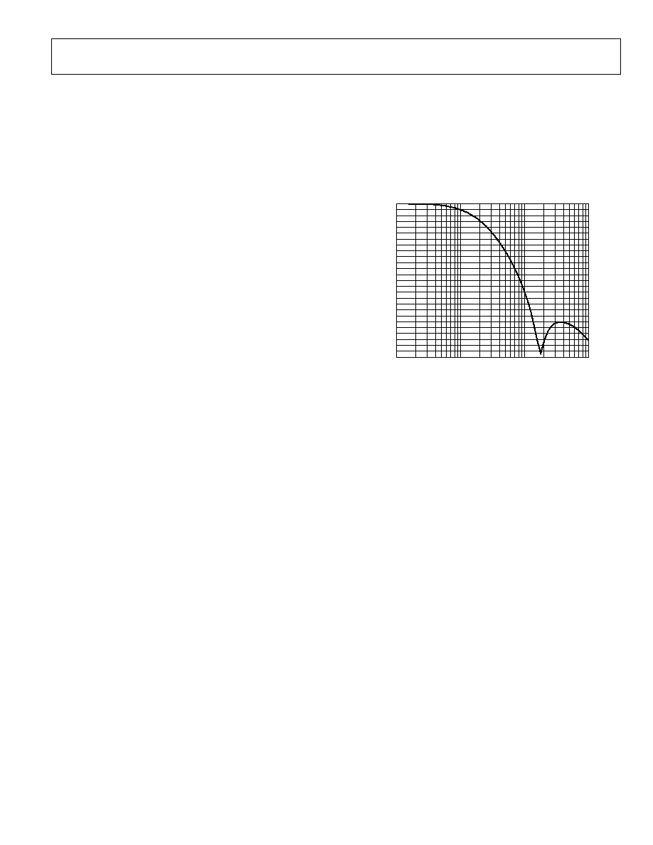
ANTIALIASING FILTERS
The ADV7188 has optional antialiasing filters on each of the
four input channels. The filters are designed for SD video with
approximately 6 MHz bandwidth.
A plot of the filter response is shown in Figure 8. The filters
can be individually enabled via I
2
C under the control of
AA_FILT_EN[3:0].
AA_FILT_EN[0], Address 0xF3 [0]
0 (default)--The filter on channel 0 is disabled
1--The filter on channel 0 is enabled
AA_FILT_EN[1], Address 0xF3 [1]
0 (default)--The filter on channel 1 is disabled
1--The filter on channel 1 is enabled
AA_FILT_EN[2], Address 0xF3 [2]
0 (default)--The filter on channel 2 is disabled
1--The filter on channel 2 is enabled
AA_FILT_EN[3], Address 0xF3 [3]
0 (default)--The filter on channel 3 is disabled
1--The filter on channel 3 is enabled
1M
1G
05478-008
FREQUENCY (Hz)
ATTE
NUATION (dB)
0
2
4
6
8
10
12
14
16
20
24
28
32
18
22
26
30
34
36
38
40
42
44
46
48
50
10M
100M
52
RESPONSE OF AA FILTER WITH CALIBRATED CAPACITORS
Figure 8. Frequency Response of Internal ADV7188 Antialiasing Filters
SCART AND FAST BLANKING
The ADV7188 can support simultaneous processing of CVBS
and RGB standard definition signals to enable SCART
compatibility and overlay functionality.
This function is available when INSEL[3:0] is set appropriately
(see Table 9). Timing extraction is always performed by the
ADV7188 on the CVBS signal. However, a combination of the
CVBS and RGB inputs can be mixed and output under control
of I
2
C registers and the fast blank (FB) pin.
Four basic modes are supported:
Static Switch Mode
The FB pin is not used. The timing is extracted from the CVBS
signal, and either the CVBS content or RGB content can be
output under the control of CVBS_RGB_SEL. This mode allows
the selection of a full-screen picture from either source. Overlay
is not possible in static switch mode.
Fixed Alpha Blending
The FB pin is not used. The timing is extracted from the CVBS
signal, and an alpha blended combination of the video from the
CVBS and RGB sources is output. This alpha blending is
applied to the full screen. The alpha blend factor is selected with
the I
2
C signal MAN_ALPHA[6:0]. Overlay is not possible in
fixed alpha blending mode.
ADV7188
Rev. 0 | Page 16 of 112
Dynamic Switching (Fast Mux)
Source selection is under the control of the fast blank (FB) pin.
This enables dynamic multiplexing between the CVBS and RGB
sources. With default settings, when Logic 1 is applied to the
FB pin, the RGB source is selected; when Logic 0 is applied to
the FB pin, the CVBS source is selected. This mode is suitable
for the overlay of subtitles, teletext, or other material. Typically,
the CVBS source carries the main picture and the RGB source
has the overlay data.
Dynamic Switching with Edge-Enhancement
This provides the same functionality as the dynamic switching
mode, but with ADI proprietary edge-enhancement algorithms
that improve the visual appearance of transitions for signals
from a wide variety of sources.
System Diagram
A block diagram of the ADV7188 fast blanking configuration is
shown in Figure 9.
The CVBS signal is processed by the ADV7188 and converted
to YPrPb. The RGB signals are processed by a color space
converter (CSC) and samples are converted to YPrPb. Both sets
of YPrPb signals are input to the sub-pixel blender, which can
be configured to operate in any of the four modes outlined
above.
The fast blank position resolver determines the time position
of the FB to a very high accuracy (<1 ns); this position infor-
mation is then used by the sub-pixel blender in dynamic
switching modes. This enables the ADV7188 to implement high
performance multiplexing between the CVBS and RGB sources,
even when the RGB data source is completely asynchronous to
the sampling crystal reference.
An anti-aliasing filter is required on all four data channels (R,
G, B, and CVBS). The order of this filter is reduced as all of the
signals are sampled at 54 MHz.
The switched or blended data is output from the ADV7188 in
the standard output formats (see Table 98).
FAST BLANK CONTROL
FB_MODE[1:0], Address 0xED [1:0]
FB_MODE controls which of the fast blank modes is selected.
Table 12: FB_MODE[1:0] function
FB_MODE[1:0] Description
00 (default)
Static Switch Mode.
01
Fixed Alpha Blending.
10
Dynamic Switching (Fast Mux).
11
Dynamic Switching with Edge Enhancement.
Static Mux Selection Control
CVBS_RGB_SEL, Address 0xED [2]
CVBS_RGB_SEL controls whether the video from the CVBS or
the RGB source is selected for output from the ADV7188.
0 (default)--Data from the CVBS source is selected for output.
1--Data from the RGB source is selected for output.
Alpha Blend Coefficient
MAN_ALPHA_VAL[6:0], Address 0xEE [6:0]
When FB_MODE[1:0] = 01 and fixed alpha blending is
selected, MAN_ALPHA_VAL[6:0] determines the proportion
in which the video from the CVBS source and the RGB source
are blended. Equation 1 shows how these bits affect the video
output.
64
]
0
:
6
[
_
_
64
]
0
:
6
[
_
_
1
VAL
ALPHA
MAN
Video
VAL
ALPHA
MAN
Video
Video
RGB
CVBS
out
×
+
-
×
=
(1)
The maximum valid value for MAN_ALPHA_VAL[6:0] is
1000000 such that the alpha blender coefficients remain
between 0 and 1. The default value for MAN_ALPHA_VAL[6:0]
is 0000000.
ADC1
R
ADC0
CVBS
ADC2
G
ADC3
B
FAST BLANK
POSITION
RESOLVER
FAST BLANK
(FB PIN)
I
2
C
CONTROL
OUTPUT
FORMATTER
YPrPb
SUBPIXEL
BLENDER
SIGNAL
CONDITIONING
CLAMPING AND
DECIMATION
TIMING
EXTRACTION
VIDEO
PROCESSING
SIGNAL
CONDITIONING
CLAMPING AND
DECIMATION
RGB
YPrPb
CONVERSION
05478-009
Figure 9. Fast Blank Block Diagram
ADV7188
Rev. 0 | Page 17 of 112
Fast Blank Edge Shaping
FB_EDGE_SHAPE[2:0], Address 0xEF [2:0]
To improve the picture transition for high speed fast blank
switching, an edge shape mode is available on the ADV7188.
Depending on the format of the RGB inputs, it may be
advantageous to apply this scheme to different degrees. The
levels are selected via the FB_EDGE_SHAPE[2:0] bits. Users are
advised to try each of the settings and select the setting that is
most visually pleasing in their system.
Table 13. FB_EDGE_SHAPE[2:0] Function
FB_EDGE_SHAPE[2:0] Description
000
No Edge Shaping.
001
Level 1 Edge Shaping.
010 (default)
Level 2 Edge Shaping.
011
Level 3 Edge Shaping.
100
Level 4 Edge Shaping.
101 to 111
Not Valid.
Contrast Reduction
For overlay applications, text can be more readable if the
contrast of the video directly behind the text is reduced. To
enable the definition of a window of reduced contrast behind
inserted text, the signal applied to the FB pin can be interpreted
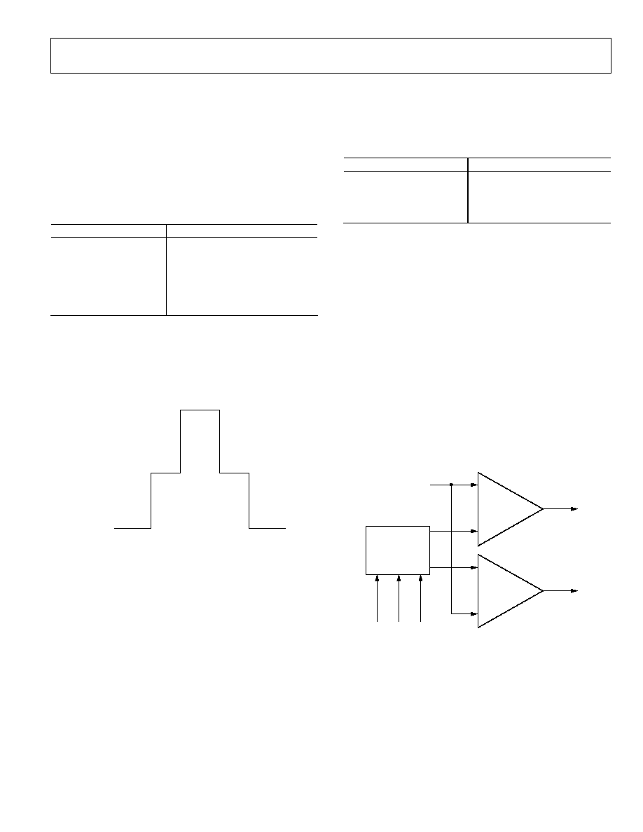
as a tri-level signal, as shown in Figure 10.
CVBS SOURCE
100%
CVBS SOURCE
50% CONTRAST
RGB SOURCE
100%
SANDCASTLE
05478-010
Figure 10. Fast Blank Signal Representation with
Contrast Reduction Enabled
Contrast Reduction Enable
CNTR_ENABLE, Address 0xEF [3]
This register enables the contrast reduction feature and changes
the meaning of the signal applied to the FB pin.
0 (default)--The contrast reduction feature is disabled and the
fast blank signal is interpreted as a bi-level signal.
1--The contrast reduction feature is enabled and the fast blank
signal is interpreted as a tri-level signal.
Contrast Mode
CNTR_MODE[1:0], Address 0xF1 [3:2]
The contrast level in the selected contrast reduction box is
selected using the CNTR_MODE[1:0] bits.
Table 14. CNTR_MODE[1:0] Function
CNTR_MODE[1:0] Description
00 (default)
25%.
01
50%.
10 75%.
11 100%.
Fast Blank and Contrast Reduction Programmable
Thresholds
FB_LEVEL[1:0], Address 0xF1 [5:4]
Controls the reference level for the fast blank comparator.
CNTR_LEVEL[1:0], Address 0xF1 [7:6]
Controls the reference level for the contrast reduction
comparator.
The internal fast blank and contrast reduction signals are
resolved from the tri-level FB signal using two comparators, as
shown in Figure 11. To facilitate compliance with different
input level standards, the reference level to these comparators is
programmable under the control of FB_LEVEL[1:0] and
CNTR_LEVEL[1:0]. The resulting thresholds are given in
Table 15.
+
PROGRAMMABLE
THRESHOLDS
+
CONTRAST
REDUCTION
COMPARATOR
C
FAST BLANK
COMPARATOR
FAST BLANK
FB PIN
CNTR E
NABLE
C
N
T
R
_
LEVEL<
1
:
0
>
FB
_LEVEL<
1
:
0
>
05478-011
Figure 11. Fast Blank and Contrast Reduction Programmable Threshold

ADV7188
Rev. 0 | Page 18 of 112
Table 15. Fast Blank and Contrast Reduction Programmable Threshold I
2
C Controls
CNTR_ENABLE FB_LEVEL[1:0] CNTR_LEVEL[1:0] Fast
Blanking Threshold
Contrast Reduction Threshold
0
00 (default)
XX
1.4 V
n/a
0 01
XX 1.6
V
n/a
0 10
XX 1.8
V
n/a
0 11
XX 2.0
V
n/a
1
00 (default)
00
1.6 V
0.4 V
1
01
01
1.8 V
0.6 V
1
10
10
2.0 V
0.8 V
1
11
11
2.2 V
2.0 V
Table 16. FB_STATUS Functions
FB_STATUS [3:0]
Bit Name
Description
0 FB_STATUS.0
FB_rise. A high value indicates there has been a rising edge on FB since the last I
2
C
read. Value is cleared by current I
2
C read self-clearing bit.
1 FB_STATUS.1
FB_fall. A high value indicates there has been a falling edge on FB since the last I
2
C
read. Value is cleared by current I
2
C read self-clearing bit.
2 FB_STATUS.2
FB_stat. Value of FB input pin at time of read.
3 FB_STATUS.3
FB_high. A high value indicates there has been a rising edge on FB since the last I
2
C
read. Value is cleared by current I
2
C read self-clearing bit.
FB_INV, Address 0xED [3] (write only)
The interpretation of the polarity of the signal applied to the FB
pin can be changed using FB_INV.
0 (default)--The fast blank pin is active high.
1--The fast blank pin is active low.
READBACK OF FB PIN STATUS
FB_STATUS[3:0], Address 0xED [7:4]
FB_STATUS[3:0] is a readback value that provides the system
information on the status of the FB pins as shown in Table 16.
FB Timing
FB_SP_ADJUST[3:0], Address 0xEF [7:4]
The critical information extracted from the FB signal is the time
at which it switches relative to the input video. Due to small
timing inequalities either on the IC or on the PCB, it may be
necessary to adjust the result by fractions of one clock cycle.
This is controlled by FB_SP_ADJUST[3:0].
Each LSB of FB_SP_ADJUST[3:0] corresponds to 1/8 of an ADC
clock cycle. Increasing the value is equivalent to adding delay to
the FB signal. The reset value is chosen to give equalized channels
when the ADV7188 internal anti-aliasing filters are enabled and
there is no unintentional delay on the PCB.
The default value of FB_SP_ADJUST[3:0] is 0100.
Alignment of FB Signal
FB_DELAY[3:0], Address 0xF0 [3:0]
In the event of misalignment between the FB input signal and
the other input signals (CVBS, RGB) or unequalized delays in
their processing, it is possible to alter the delay of the FB signal
in 28.63636 MHz clock cycles. (For a finer granularity delay of
the FB signal, refer to FB_SP_ADJUST[3:0], Address 0xEF [7:4]
above.)
The default value of FB_DELAY[3:0] is 0100.
Color Space Converter Manual Adjust
FB_CSC_MAN, Address 0xEE [7]
As shown in Figure 9, the data from the CVBS source and the
RGB source are both converted to YPbPr before being combined.
For the RGB source, the color space converter (CSC) must be
used to perform this conversion. When SCART support is
enabled, the parameters for the CSC are automatically
configured correctly for this operation.
If the user wishes to use a different conversion matrix, this
autoconfiguration can be disabled and the CSC can be manually
programmed. For details on this manual configuration, please
contact ADI.
0 (default)--The CSC is configured automatically for the RGB
to YPrPb conversion.
1--The CSC can be configured manually (not recommended).

ADV7188
Rev. 0 | Page 19 of 112
GLOBAL CONTROL REGISTERS
Register control bits listed in this section affect the whole chip.
POWER-SAVE MODES
Power-Down
PDBP, Address 0x0F [2]
The digital core of the ADV7188 can be shut down by using a
pin (PWRDN) and the PWRDN bit. The PDBP register
controls which of the two has the higher priority. The default is
to give the pin (PWRDN) priority. This allows the user to have
the ADV7188 powered down by default.
0 (default)--The digital core power is controlled by the
PWRDN pin (the bit is disregarded).
1--The bit has priority (the pin is disregarded).
PWRDN, Address 0x0F [5]
Setting the PWRDN bit switches the ADV7188 into a chip-wide
power-down mode. The power-down stops the clock from
entering the digital section of the chip, thereby freezing its
operation. No I
2
C bits are lost during power-down. The
PWRDN bit also affects the analog blocks and switches them
into low current modes. The I
2
C interface itself is unaffected,
and remains operational in power-down mode.
The ADV7188 leaves the power-down state if the PWRDN bit is
set to 0 (via I
2
C), or if the overall part is reset using the RESET
pin. Note that PDBP must be set to 1 for the PWRDN bit to
power down the ADV7188.
0 (default)--The chip is operational.
1--The ADV7188 is in chip-wide power-down.
ADC Power-Down Control
The ADV7188 contains four 12-bit ADCs (ADC 0, ADC 1,
ADC 2 and ADC 3). If required, it is possible to power down
each ADC individually.
·
In CVBS mode, ADC1 and ADC2 should be powered
down to save on power consumption.
·
In S-Video mode, ADC2 should be powered down to save
on power consumption.
PWRDN_ADC_0, Address 0x3A [3]
0 (default)--The ADC is in normal operation.
1--ADC0 is powered down.
PWRDN_ADC_1, Address 0x3A [2]
0 (default)--The ADC is in normal operation.
1--ADC1 is powered down.
PWRDN_ADC_2, Address 0x3A [1]
0 (default)--The ADC is in normal operation.
1--ADC2 is powered down.
PWRDN_ADC_3, Address 0x3A [0]
0 (default)--The ADC is in normal operation.
1--ADC3 is powered down.
FB_PWRDN, Address 0x0F [1]
To achieve very low power-down current, it is necessary to
prevent activity on toggling input pins from reaching circuitry
that could consume current. FB_PWRDN gates signals from the
FB input pin.
0 (default)--The FB input is in normal operation.
1--The FB input is in power-save mode.
RESET CONTROL
RES Chip Reset, Address 0x0F [7]
Setting this bit, equivalent to controlling the RESET pin on the
ADV7188, issues a full chip reset. All I
2
C registers are reset to
their default values, making these bits self-clearing. Some
register bits do not have a reset value specified. They keep their
last written value. Those bits are marked as having a reset value
of x in the register tables. After the reset sequence, the part
immediately starts to acquire the incoming video signal.
Executing a software reset takes approximately 2 ms. However,
it is recommended to wait 5 ms before performing any more I
2
C
writes.
The I
2
C master controller receives a no acknowledge condition
on the ninth clock cycle when chip reset is implemented. See
the MPU Port Description section for a full description.
0 (default)--Operation is normal.
1--The reset sequence starts.
GLOBAL PIN CONTROL
Three-State Output Drivers
TOD, Address 0x03 [6]
This bit allows the user to three-state the output drivers of the
ADV7188. Upon setting the TOD bit, the P19 to P0, HS, VS,
FIELD, and SFL pins are three-stated. The ADV7188 also
supports three-stating via a dedicated pin, OE. The output
drivers are three-stated if the TOD bit or the OE pin is set high.
The timing pins (HS/VS/FIELD) can be forced active via the
TIM_OE bit. For more information on three-state control, refer
to the Three-State LLC Drivers and the Timing Signals Output
Enable sections. Individual drive strength controls are provided
by the DR_STR_XX bits.
0 (default)--The output drivers are enabled.
1--The output drivers are three-stated.

ADV7188
Rev. 0 | Page 20 of 112
Three-State LLC Drivers
TRI_LLC, Address 0x1D [7]
This bit allows the output drivers for the LLC1 and LLC2 pins
of the ADV7188 to be three-stated. For more information on
three-state control, refer to the Three-State Output Drivers and
the Timing Signals Output Enable sections. Individual drive
strength controls are provided via the DR_STR_XX bits.
0 (default)--The LLC pin drivers work according to the
DR_STR_C[1:0] setting (pin enabled).
1--The LLC pin drivers are three-stated.
Timing Signals Output Enable
TIM_OE, Address 0x04 [3]
The TIM_OE bit should be regarded as an addition to the TOD
bit. Setting it high forces the output drivers for HS, VS, and
FIELD into the active (that is, driving) state even if the TOD bit
is set. If set to low, the HS, VS, and FIELD pins are three-stated
dependent on the TOD bit. This functionality is useful if the
decoder is to be used as a timing generator only. This may be
the case if only the timing signals are to be extracted from an
incoming signal, or if the part is in free-run mode where, for
example, a separate chip can output a company logo. For more
information on three-state control, refer to the Three-State
Output Drivers and the Three-State LLC Drivers sections.
Individual drive strength controls are provided via the
DR_STR_XX bits.
0 (default)--HS, VS, and FIELD are three-stated according to
the TOD bit.
1--HS, VS, and FIELD are forced active all the time.
Drive Strength Selection (Data)
DR_STR[1:0], Address 0xF4 [5:4]
For EMC and crosstalk reasons, it may be desirable to
strengthen or weaken the drive strength of the output drivers.
The DR_STR[1:0] bits affect the P[19:0] output drivers.
For more information on three-state control, refer to the Drive
Strength Selection (Clock) and the Drive Strength Selection
(Sync) sections.
Table 17. DR_STR_C Function
DR_STR_C[1:0] Description
01 (default)
Medium low drive strength (2×).
10
Medium high drive strength (3×).
11
High drive strength (4×).
Drive Strength Selection (Clock)
DR_STR_C[1:0] Address 0xF4 [3:2]
The DR_STR_C[1:0] bits can be used to select the strength of
the clock signal output driver (LLC pin). For more information,
refer to the Drive Strength Selection (Sync) and the Drive
Strength Selection (Data) sections.
Table 18. DR_STR_C Function
DR_STR_C[1:0] Description
01 (default)
Medium low drive strength (2×).
10
Medium high drive strength (3×).
11
High drive strength (4×).
Drive Strength Selection (Sync)
DR_STR_S[1:0], Address 0xF4 [1:0]
The DR_STR_S[1:0] bits allow the user to select the strength of
the synchronization signals with which HS, VS, and F are driven.
For more information, refer to the Drive Strength Selection
(Clock) and the Drive Strength Selection (Data) sections.
Table 19. DR_STR_S Function
DR_STR_S[1:0] Description
01 (default)
Medium low drive strength (2×).
10
Medium high drive strength (3×).
11
High drive strength (4×).
Enable Subcarrier Frequency Lock Pin
EN_SFL_PIN, Address 0x04 [1]
The EN_SFL_PIN bit enables the output of subcarrier lock
information (also known as GenLock) from the ADV7188 core
to an encoder in a decoder-encoder back-to-back arrangement.
0 (default)--The subcarrier frequency lock output is disabled.
1--The subcarrier frequency lock information is presented on
the SFL pin.
Polarity LLC Pin
PCLK, Address 0x37 [0]
The polarity of the clock that leaves the ADV7188 via the LLC1
and LLC2 pins can be inverted using the PCLK bit. Changing
the polarity of the LLC clock output may be necessary to meet
the setup-and-hold time expectations of follow-on chips. This
bit also inverts the polarity of the LLC2 clock.
0--The LLC output polarity is inverted.
1 (default)--The LLC output polarity is normal (as per the
timing diagrams).
ADV7188
Rev. 0 | Page 21 of 112
GLOBAL STATUS REGISTERS
Three registers provide summary information about the video
decoder. The STATUS_1, STATUS_2, and STATUS_3 registers
contain status bits that report operational information to the user.
STATUS_1[7:0] Address 0x10 [7:0]
This read only register provides information about the internal
status of the ADV7188. See CIL[2:0] Count Into Lock, Address
0x51 [2:0] and COL[2:0] Count Out of Lock, Address 0x51 [5:3]
for information on the timing.
Depending on the setting of the FSCLE bit, the STATUS_1[0]
and STATUS_1[1] bits are based solely on horizontal timing
information or on the horizontal timing and lock status of the
color subcarrier. See the FSCLE Fsc Lock Enable, Address 0x51
[7] section.
STATUS_2[7:0], Address 0x12 [7:0]
See Table 22.
STATUS_3[7:0], Address 0x13 [7:0]
See Table 23.
AD_RESULT[2:0] Autodetection Result Address 0x10 [6:4]
These bits report back on the findings from the autodetection
block. For more information on enabling the autodetection
block, see the General Setup section. For information on
configuring it, see the Autodetection of SD Modes section.
Table 20. AD_RESULT Function
AD_RESULT[2:0] Description
000 NTSM-MJ
001 NTSC-443
010 PAL-M
011 PAL-60
100 PAL-BGHID
101 SECAM
110 PAL-Combination
N
111 SECAM
525
Table 21. STATUS_1 Function
STATUS 1 [7:0]
Bit Name
Description
0
IN_LOCK
In lock (right now).
1
LOST_LOCK
Lost lock (since last read of this register).
2
FSC_LOCK
Fsc locked (right now).
3 FOLLOW_PW
AGC
follows
peak white algorithm.
4
AD_RESULT.0
Result of autodetection.
5
AD_RESULT.1
Result of autodetection.
6
AD_RESULT.2
Result of autodetection.
7
COL_KILL
Color kill active.
Table 22. STATUS_2 Function
STATUS 2 [7:0]
Bit Name
Description
0
MVCS DET
Detected Macrovision color striping.
1
MVCS T3
Macrovision color striping protection. Conforms to Type 3 if high, and to Type 2 if low.
2
MV_PS DET
Detected Macrovision pseudo Sync pulses.
3
MV_AGC DET
Detected Macrovision AGC pulses.
4
LL_NSTD
Line length is nonstandard.
5
FSC_NSTD
Fsc frequency is nonstandard.
6 Reserved
7 Reserved
Table 23. STATUS_3 Function
STATUS 3 [7:0]
Bit Name
Description
0 INST_HLOCK
Horizontal
lock indicator (instantaneous).
1 GEMD
Gemstar
detect.
2
SD_OP_50HZ
Flags whether 50 Hz or 60 Hz is present at output.
3
CVBS
Indicates if a CVBS signal is detected in `YC/CVBS autodetection' configuration
4 FREE_RUN_ACT
Indicates if the ADV7188 is in free run mode. Outputs a blue screen by default. See the
DEF_VAL_AUTO_EN Default Value Automatic Enable, Address 0x0C [1] bit for details about
disabling this function.
5
STD_FLD_LEN
Field length is correct for currently selected video standard.
6
INTERLACED
Interlaced video detected (field sequence found).
7
PAL_SW_LOCK
Reliable sequence of swinging bursts detected.
ADV7188
Rev. 0 | Page 22 of 112
STANDARD DEFINITION PROCESSOR (SDP)
05478-012
DIGITIZED CVBS
DIGITIZED Y (YC)
VIDEO DATA
OUTPUT
STANDARD DEFINITION PROCESSOR
DIGITIZED CVBS
DIGITIZED C (YC)
MACROVISION
DETECTION
VBI DATA
RECOVERY
STANDARD
AUTODETECTION
LUMA
FILTER
LUMA
DIGITAL
FINE
CLAMP
GAIN
CONTROL
LUMA
RESAMPLE
LUMA
2D COMB
SLLC
CONTROL
CHROMA
FILTER
CHROMA
DEMOD
F
SC
RECOVERY
CHROMA
DIGITAL
FINE
CLAMP
GAIN
CONTROL
CHROMA
RESAMPLE
CHROMA
2D COMB
SYNC
EXTRACT
LINE
LENGTH
PREDICTOR
RESAMPLE
CONTROL
AV
CODE
INSERTION
MEASUREMENT
BLOCK (= >1
2
C)
VIDEO DATA
PROCESSING
BLOCK
Figure 12. Block Diagram of the Standard Definition Processor
A block diagram of the ADV7188's standard definition
processor (SDP) is shown in Figure 12.
The SDP block can handle standard definition video in CVBS,
YC, and YPrPb formats. It can be divided into a luminance and
a chrominance path. If the input video is of a composite type
(CVBS), both processing paths are fed with the CVBS input.
SD LUMA PATH
The input signal is processed by the following blocks:
Digital Fine Clamp. This block uses a high precision algorithm
to clamp the video signal.
Luma Filter Block. This block contains a luma decimation filter
(YAA) with a fixed response, and some shaping filters (YSH)
that have selectable responses.
Luma Gain Control. The automatic gain control (AGC) can
operate on a variety of different modes, including gain based on
the depth of the horizontal sync pulse, peak white mode, and
fixed manual gain.
Luma Resample. To correct for line-length errors and dynamic
line-length changes, the data is digitally resampled.
Luma 2D Comb. The two-dimensional comb filter provides YC
separation.
AV Code Insertion. At this point, the decoded luma (Y) signal
is merged with the retrieved chroma values. AV codes (as per
ITU-R. BT-656) can be inserted.
SD CHROMA PATH
The input signal is processed by the following blocks:
Digital Fine Clamp. This block uses a high precision algorithm
to clamp the video signal.
Chroma Demodulation. This block uses a color subcarrier (Fsc)
recovery unit to regenerate the color subcarrier for any
modulated chroma scheme. The demodulation block then
performs an AM demodulation for PAL and NTSC and an FM
demodulation for SECAM.
Chroma Filter Block. This block contains a chroma decimation
filter (CAA) with a fixed response, and some shaping filters
(CSH) that have selectable responses.
Gain Control. Automatic gain control (AGC) can operate on
several different modes, including gain based on the color
subcarrier's amplitude, gain based on the depth of the
horizontal sync pulse on the luma channel, or fixed manual
gain.
Chroma Resample. The chroma data is digitally resampled to
keep it perfectly aligned with the luma data. The resampling is
done to correct for static and dynamic line-length errors of the
incoming video signal.
Chroma 2D Comb. The two-dimensional, 5-line, superadaptive
comb filter provides high quality YC separation in case the
input signal is CVBS.
AV Code Insertion. At this point, the demodulated chroma (Cr
and Cb) signal is merged with the retrieved luma values. AV
codes (as per ITU-R. BT-656) can be inserted.

ADV7188
Rev. 0 | Page 23 of 112
SYNC PROCESSING
The ADV7188 extracts syncs embedded in the video data
stream. There is currently no support for external HS/VS
inputs. The sync extraction has been optimized to support
imperfect video sources such as videocassette recorders with
head switches. The actual algorithm used employs a coarse
detection based on a threshold crossing, followed by a more
detailed detection using an adaptive interpolation algorithm.
The raw sync information is sent to a line-length measurement
and prediction block. The output of this block is then used to
drive the digital resampling section to ensure that the ADV7188
outputs 720 active pixels per line.
The sync processing on the ADV7188 also includes the following
specialized postprocessing blocks that filter and condition the raw
sync information retrieved from the digitized analog video.
·
VSYNC Processor. This block provides extra filtering of the
detected VSYNCs to give improved vertical lock.
·
HSYNC Processor. The HSYNC processor is designed to
filter incoming HSYNCs that have been corrupted by
noise, providing much improved performance for video
signals with stable time base but poor SNR.
VBI DATA RECOVERY
The ADV7188 can retrieve the following information from the
input video:
·
Wide-screen signaling (WSS)
·
Copy generation management system (CGMS)
·
Closed caption (CC)
·
Macrovision protection presence
·
Gemstar-compatible data slicing
·
Teletext
The ADV7188 is also capable of automatically detecting the
incoming video standard with respect to
·
Color subcarrier frequency
·
Field rate
·
Line rate
The ADV7188 can configure itself to support PAL-
(B/G/H/I/D/M/N), PAL-combination N, NTSC-M, NTSC-J,
SECAM 50 Hz/60 Hz, NTSC-4.43, and PAL-60.
GENERAL SETUP
Video Standard Selection
The VID_SEL[3:0] register allows the user to force the digital
core into a specific video standard. Under normal circumstances,
this should not be necessary. The VID_SEL[3:0] bits default to
an autodetection mode that supports PAL, NTSC, SECAM, and
variants thereof. The following section describes the autodetec-
tion system.
Autodetection of SD Modes
In order to guide the autodetect system, individual enable bits
are provided for each of the supported video standards. Setting
the relevant bit to 0 inhibits the standard from being automatically
detected. Instead, the system picks the closest of the remaining
enabled standards. The results of the autodetection can be read
back via the status registers. See the Global Status Registers
section for more information.
VID_SEL[3:0] Address 0x00 [7:4]
Table 24. VID_SEL Function
VID_SEL[3:0] Description
0000 (default)
Autodetect (PAL-BGHID) <> NTSC-J
(without pedestal), SECAM
0001
Autodetect (PAL-BGHID) <> NTSC-M
(with pedestal), SECAM
0010
Autodetect (PAL N) (pedestal) <> NTSC-J
(no pedestal), SECAM
0011
Autodetect (PAL N) (with pedestal) <> NTSC-M
(with pedestal), SECAM
0100 NTSC-J
(1)
0101 NTSC-M
(1)
0110 PAL-60
0111 NTSC-4.43
(1)
1000 PAL-BGHID.
1001
PAL-N (= PAL BGHID (with pedestal))
1010
PAL-M (without pedestal)
1011 PAL-M
1100 PAL-combination
N
1101
PAL-combination N (with pedestal)
1110 SECAM
1111
SECAM (with pedestal)
AD_SEC525_EN Enable Autodetection of SECAM 525
Line Video, Address 0x07 [7]
0 (default)--Disables the autodetection of a 525-line system
with a SECAM style, FM-modulated color component.
1--Enables autodetection.
AD_SECAM_EN Enable Autodetection of SECAM,
Address 0x07 [6]
0--Disables the autodetection of SECAM.
1 (default)--Enables autodetection.

ADV7188
Rev. 0 | Page 24 of 112
AD_N443_EN Enable Autodetection of NTSC 443,
Address 0x07 [5]
0--Disables the autodetection of NTSC style systems with a
4.43 MHz color subcarrier.
1 (default)--Enables autodetection.
AD_P60_EN Enable Autodetection of PAL-60,
Address 0x07 [4]
0--Disables the autodetection of PAL systems with a 60 Hz
field rate.
1 (default)--Enables autodetection.
AD_PALN_EN Enable Autodetection of PAL-N,
Address 0x07 [3]
0--Disables the autodetection of the PAL -N standard.
1 (default)--Enables autodetection.
AD_PALM_EN Enable Autodetection of PAL-M,
Address 0x07 [2]
0--Disables the autodetection of PAL-M.
1 (default)--Enables autodetection.
AD_NTSC_EN Enable Autodetection of NTSC,
Address 0x07 [1]
0--Disables the autodetection of standard NTSC.
1 (default)--Enables autodetection.
AD_PAL_EN Enable Autodetection of PAL,
Address 0x07 [0]
0--Disables the autodetection of standard PAL.
1 (default)--Enables autodetection.
Subcarrier Frequency Lock Inversion
The SFL_INV bit controls the behavior of the PAL switch bit in
the SFL (GenLock Telegram) data stream. It was implemented
to solve some compatibility issues with video encoders. It solves
two problems.
First, the PAL switch bit is only meaningful in PAL. Some
encoders (including Analog Devices encoders) also look at the
state of this bit in NTSC.
Second, there was a design change in Analog Devices encoders
from ADV717x to ADV719x. The older versions used the SFL
(GenLock Telegram) bit directly, while the later ones invert the
bit prior to using it. The reason for this is that the inversion
compensated for the 1-line delay of an SFL (GenLock Telegram)
transmission.
As a result, ADV717x encoders need the PAL switch bit in the
SFL (GenLock Telegram) to be 1 for NTSC to work. Also, the
ADV7190/ADV7191/ADV7194 encoders need the PAL switch
bit in the SFL to be 0 to work in NTSC. If the state of the PAL
switch bit is wrong, a 180°phase shift occurs.
In a decoder/encoder back-to-back system in which SFL is used,
this bit must be set up properly for the specific encoder used.
SFL_INV Address 0x41 [6]
0 (default)--Makes the part SFL-compatible with ADV7190/
ADV7191/ADV7194 and ADV73xx encoders.
1--Makes the part SFL-compatible with ADV717x encoders.
Lock-Related Controls
Lock information is presented to the user through Bits [1:0] of
the Status 1 register. See the STATUS_1[7:0] Address 0x10 [7:0]
section. Figure 13 outlines the signal flow and the controls
available to influence the way the lock status information is
generated.
SRLS Select Raw Lock Signal, Address 0x51 [6]
Using the SRLS bit, the user can choose between two sources for
determining the lock status (per Bits [1:0] in the Status 1
register).
The time_win signal is based on a line-to-line evaluation of the
horizontal synchronization pulse of the incoming video. It reacts
quite quickly.
The free_run signal evaluates the properties of the incoming
video over several fields, and takes vertical synchronization
information into account.
0 (default)--Selects the free_run signal.
1--Selects the time_win signal.
05478-013
1
0
TIME_WIN
FREE_RUN
STATUS 1 [0]
SELECT THE RAW LOCK SIGNAL
SRLS
FILTER THE RAW LOCK SIGNAL
CIL[2:0], COL[2:0]
TAKE F
SC
LOCK INTO ACCOUNT
FSCLE
STATUS 1 [1]
F
SC
LOCK
1
0
COUNTER INTO LOCK
COUNTER OUT OF LOCK
MEMORY
Figure 13. Lock-Related Signal Path

ADV7188
Rev. 0 | Page 25 of 112
FSCLE Fsc Lock Enable, Address 0x51 [7]
The FSCLE bit allows the user to choose whether the status of the
color subcarrier loop is taken into account when the overall lock
status is determined and presented via Bits [1:0] in STATUS_1.
This bit must be set to 0 when operating in YPrPb component
mode to generate a reliable HLOCK status bit.
0 (default)--Makes the overall lock status dependent on the
horizontal sync lock.
1--Makes the overall lock status dependent on the horizontal
sync lock and Fsc lock.
VS_Coast[1:0], Address 0xF9 [3:2]
These bits are used to set VS free-run (coast) frequency.
Table 25. VS_COAST[1:0] function
VS_COAST [1:0]
Description
00 (default)
Auto coast Mode follows VS
frequency from last video input
01
Forces 50 Hz coast Mode
10
Forces 60 Hz coast Mode
11 Reserved
CIL[2:0] Count Into Lock, Address 0x51 [2:0]
CIL[2:0] determines the number of consecutive lines for which
the into-lock condition must be true before the system switches
into the locked state, and reports this via STATUS_1[1:0]. It
counts the value in lines of video.
Table 26. CIL Function
CIL[2:0] Description
000 1
001 2
010 5
011 10
100 (default)
100
101 500
110 1000
111 100000
COL[2:0] Count Out of Lock, Address 0x51 [5:3]
COL[2:0] determines the number of consecutive lines for which
the out-of-lock condition must be true before the system switches
into unlocked state, and reports this via STATUS_0[1:0]. It
counts the value in lines of video.
Table 27. COL Function
COL[2:0] Description
000 1
001 2
010 5
011 10
100 (default)
100
101 500
110 1000
111 100000
ST_NOISE_VLD, HS Tip Noise Measurement Valid, Address
0xDE [3] (read only)
0--The ST_NOISE[10:0] measurement is not valid
1 (default)--The ST_NOISE[10:0] measurement is valid.
ST_NOISE[10:0] HS Tip Noise Measurement, Address 0xDE
[2:0], 0xDF [7:0]
The ST_NOISE[10:0] measures, over four fields, a readback
value of the average of the noise in the HSYNC tip.
ST_NOISE_VLD must be 1 for this measurement to be valid.
1 bit of ST_NOISE[10:0] = 1 ADC code.
1 bit of ST_NOISE[10:0] = 1.6 V/4096 = 390.625 V.
COLOR CONTROLS
These registers allow the user to control the picture appearance,
including control of the active data in the event of video being
lost. These controls are independent of any other controls. For
instance, brightness control is independent of picture clamping,
although both controls affect the signal's dc level.
CON[7:0] Contrast Adjust, Address 0x08 [7:0]
This register allows the user to adjust the contrast of the picture.
Table 28. CON Function
CON[7:0] Description
0x80 (default)
Gain on luma channel = 1
0x00
Gain on luma channel = 0
0xFF
Gain on luma channel = 2
SD_SAT_Cb[7:0] SD Saturation Cb Channel, Address 0xE3 [7:0]
This register allows the user to control the gain of the Cb channel
only. The user can adjust the saturation of the picture.
Table 29. SD_SAT_Cb Function
SD_SAT_Cb[7:0] Description
0x80 (default)
Gain on Cb channel = 1
0x00
Gain on Cb channel = 0
0xFF
Gain on Cb channel = 2

ADV7188
Rev. 0 | Page 26 of 112
SD_SAT_Cr[7:0] SD Saturation Cr Channel, Address 0xE4 [7:0]
This register allows the user to control the gain of the Cr
channel only. The user can adjust the saturation of the picture.
Table 30. SD_SAT_Cr Function
SD_SAT_Cr[7:0] Description
0x80 (default)
Gain on Cr channel = 1
0x00
Gain on Cr channel = 0
0xFF
Gain on Cr channel = 2
SD_OFF_Cb[7:0] SD Offset Cb Channel, Address 0xE1 [7:0]
This register allows the user to select an offset for data on the
Cb channel only and adjust the hue of the picture. There is a
functional overlap with the HUE[7:0] register.
Table 31. SD_OFF_Cb Function
SD_OFF_Cb[7:0] Description
0x80 (default)
0 offset applied to the Cb channel.
0x00
-568 mV offset applied to the Cb channel.
0xFF
+568 mV offset applied to the Cb channel.
SD_OFF_Cr [7:0] SD Offset Cr Channel, Address 0xE2 [7:0]
This register allows the user to select an offset for data on the Cr
channel only and adjust the hue of the picture. There is a func-
tional overlap with the HUE[7:0] register.
Table 32. SD_OFF_Cr Function
SD_OFF_Cr[7:0] Description
0x80 (default)
0 offset applied to the Cr channel.
0x00
-568 mV offset applied to the Cr channel.
0xFF
+568 mV offset applied to the Cr channel.
BRI[7:0] Brightness Adjust, Address 0x0A [7:0]
This register controls the brightness of the video signal. It
allows the user to adjust the brightness of the picture.
Table 33. BRI Function
BRI[7:0] Description
0x00 (default)
Offset of the luma channel = 0mV
0x7F
Offset of the luma channel = +204mV
0x80
Offset of the luma channel = -204mV
HUE[7:0] Hue Adjust, Address 0x0B [7:0]
This register contains the value for the color hue adjustment. It
allows the user to adjust the hue of the picture.
HUE[7:0] has a range of ±90°, with 0x00 equivalent to an
adjustment of 0°. The resolution of HUE[7:0] is 1 bit = 0.7°.
The hue adjustment value is fed into the AM color demodulation
block. Therefore, it only applies to video signals that contain
chroma information in the form of an AM modulated carrier
(CVBS or Y/C in PAL or NTSC). It does not affect SECAM and
does not work on component video inputs (YPrPb).
Table 34. HUE Function
HUE[7:0] Description
0x00 (default)
Phase of the chroma signal = 0°.
0x7F
Phase of the chroma signal = +90°.
0x80
Phase of the chroma signal = -90°.
DEF_Y[5:0] Default Value Y, Address 0x0C [7:2]
If the ADV7188 loses lock on the incoming video signal or if
there is no input signal, the DEF_Y[5:0] bits allow the user to
specify a default luma value to be output. The register is used
under the following conditions:
·
If DEF_VAL_AUTO_EN bit is set to high and the
ADV7188 loses lock to the input video signal. This is the
intended mode of operation (automatic mode).
·
The DEF_VAL_EN bit is set, regardless of the lock status of
the video decoder. This is a forced mode that may be useful
during configuration.
The DEF_Y[5:0] values define the 6 MSBs of the output video.
The remaining LSBs are padded with 0s. For example, in 10-bit
mode, the output is Y[9:0] = {DEF_Y[5:0], 0, 0, 0, 0}.
The value for Y is set by the DEF_Y[5:0] bits. A value of 0x0D
produces a blue color in conjunction with the DEF_C[7:0]
default setting.
Register 0x0C has a default value of 0x36.
DEF_C[7:0] Default Value C, Address 0x0D [7:0]
The DEF_C[7:0] register complements the DEF_Y[5:0] value.
It defines the 4 MSBs of Cr and Cb values to be output if
·
The DEF_VAL_AUTO_EN bit is set to high and the
ADV7188 can't lock to the input video (automatic mode).
·
DEF_VAL_EN bit is set to high (forced output).
The data that is finally output from the ADV7188 for the
chroma side is Cr[7:0] = {DEF_C[7:4], 0, 0, 0, 0}, Cb[7:0] =
{DEF_C[3:0], 0, 0, 0, 0}.
In full 10-bit output mode, two extra LSBs of value 00 are
appended.
The values for Cr and Cb are set by the DEF_C[7:0] bits. A
value of 0x7C produces a blue color in conjunction with the
DEF_Y[5:0] default setting.

ADV7188
Rev. 0 | Page 27 of 112
DEF_VAL_EN Default Value Enable, Address 0x0C [0]
This bit forces the use of the default values for Y, Cr, and Cb.
Refer to the descriptions for DEF_Y and DEF_C for additional
information. In this mode, the decoder also outputs a stable
27 MHz clock, HS, and VS.
0 (default)--Outputs a colored screen determined by user-
programmable Y, Cr, and Cb values when the decoder free-
runs. Free-run mode is turned on and off by the
DEF_VAL_AUTO_EN bit.
1--Forces a colored screen output determined by user-
programmable Y, Cr, and Cb values. This overrides picture
data even if the decoder is locked.
DEF_VAL_AUTO_EN Default Value Automatic Enable,
Address 0x0C [1]
This bit enables the automatic use of the default values for Y, Cr,
and Cb when the ADV7188 cannot lock to the video signal.
0--Disables free-run mode. If the decoder is unlocked, it
outputs noise.
1 (default)--Enables free-run mode. A colored screen set by the
user-programmable Y, Cr, and Cb values is displayed when the
decoder loses lock.
CLAMP OPERATION
The input video is ac-coupled into the ADV7188 through a
0.1 F capacitor. It is recommended that the range of the input
video signal is 0.5 V to 1.6 V (typically 1 V
p-p). If the signal
exceeds this range, it cannot be processed correctly in the
decoder. Since the input signal is ac-coupled into the decoder,
its dc value needs to be restored. This process is referred to as
clamping the video. This section explains the general process of
clamping on the ADV7188 and shows the different ways in
which a user can configure its behavior.
The ADV7188 uses a combination of current sources and a
digital processing block for clamping, as shown in Figure 14.
The analog processing channel shown is replicated three times
inside the IC. While only one single-channel (and only one
ADC) is needed for a CVBS signal, two independent channels
are needed for YC (S-VHS) type signals, and three independent
channels are needed to allow component signals (YPrPb) to be
processed.
The clamping can be divided into two sections
·
Clamping before the ADC (analog domain): current
sources.
·
Clamping after the ADC (digital domain): digital
processing block.
The ADCs can digitize an input signal only if it resides within
their 1.6 V input voltage range. An input signal with a dc level
that is too large or too small is clipped at the top or bottom of
the ADC range.
The primary task of the analog clamping circuits is to ensure
that the video signal stays within the valid ADC input window
so that the analog-to-digital conversion can take place. It is not
necessary to clamp the input signal with a very high accuracy in
the analog domain as long as the video signal fits the ADC range.
After digitization, the digital fine clamp block corrects for any
remaining variations in dc level. Since the dc level of an input
video signal refers directly to the brightness of the picture
transmitted, it is important to perform a fine clamp with high
accuracy; otherwise, brightness variations may occur. Further-
more, dynamic changes in the dc level almost certainly lead to
visually objectionable artifacts, and must therefore be prohibited.
The clamping scheme must be able to acquire a newly
connected video signal with a completely unknown dc level,
and it must maintain the dc level during normal operation.
To quickly acquire an unknown video signal, the large current
clamps may be activated. It is assumed that the amplitude of the
video signal at this point is of a nominal value. Control of the
coarse and fine current clamp parameters is automatically
performed by the decoder.
Standard definition video signals may have excessive noise on
them. In particular, CVBS signals transmitted by terrestrial
broadcast and demodulated using a tuner usually show very
large levels of noise (>100 mV). A voltage clamp would be
unsuitable for this type of video signal. Instead, the ADV7188
uses a set of four current sources that can cause coarse
(>0.5 mA) and fine (<0.1 mA) currents to flow into and away
from the high impedance node that carries the video signal (see
Figure 14).
The following sections describe the I
2
C signals that can be used to
influence the behavior of the clamping block on the ADV7188.
CCLEN Current Clamp Enable, Address 0x14 [4]
The current clamp enable bit allows the user to switch off the
current sources in the analog front end altogether. This may be
useful if the incoming analog video signal is clamped externally.
0--The current sources are switched off.
1 (default)--The current sources are enabled.
ADV7188
Rev. 0 | Page 28 of 112
05478-014
COARSE
CURRENT
SOURCES
FINE
CURRENT
SOURCES
DATA
PRE-
PROCESSOR
(DPP)
ADC
SDP
WITH DIGITAL
FINE CLAMP
CLAMP CONTROL
ANALOG
VIDEO
INPUT
Figure 14. Clamping Overview
DCT[1:0] Digital Clamp Timing, Address 0x15 [6:5]
The clamp timing register determines the time constant of the
digital fine clamp circuitry. It is important to realize that the
digital fine clamp reacts very quickly since it is supposed to
immediately correct any residual dc level error for the active
line. The time constant of the digital fine clamp must be much
quicker than the one from the analog blocks.
By default, the time constant of the digital fine clamp is adjusted
dynamically to suit the currently connected input signal.
Table 35. DCT Function
DCT[1:0] Description
00
Slow (TC = 1 sec).
01
Medium (TC = 0.5 sec).
10 (default)
Fast (TC = 0.1 sec).
11
Determined by the ADV7188, depending on
the I/P video parameters.
DCFE Digital Clamp Freeze Enable, Address 0x15 [4]
This register bit allows the user to freeze the digital clamp loop
at any time. It is intended for users who would like to do their
own clamping. Users should disable the current sources for
analog clamping via the appropriate register bits, wait until the
digital clamp loop settles, and then freeze it via the DCFE bit.
0 (default)--The digital clamp is operational.
1--The digital clamp loop is frozen.
LUMA FILTER
Data from the digital fine clamp block is processed by three sets
of filters. The data format at this point is CVBS for CVBS input
or luma only for Y/C and YPrPb input formats.
·
Luma antialias filter (YAA). The ADV7188 receives video
at a rate of 27 MHz. (For 4× oversampled video, the ADCs
sample at 54 MHz, and the first decimation is performed
inside the DPP filters. Therefore, the data rate into the
ADV7188 is always 27 MHz.) The ITU-R BT.601 recommends
a sampling frequency of 13.5 MHz. The luma antialias
filter decimates the oversampled video using a high quality,
linear phase, low-pass filter that preserves the luma signal
while at the same time attenuating out-of-band components.
The luma antialias filter has a fixed response.
·
Luma shaping filters (YSH). The shaping filter block is a
programmable low-pass filter with a wide variety of re-
sponses. It can be used to selectively reduce the luma video
signal bandwidth (needed prior to scaling, for example).
For some video sources that contain high frequency noise,
reducing the bandwidth of the luma signal improves visual
picture quality. A follow-on video compression stage may
work more efficiently if the video is low-pass filtered.
The ADV7188 has two responses for the shaping filter: one
that is used for good quality CVBS, component, and S-VHS
type sources, and a second for nonstandard CVBS signals.
The YSH filter responses also include a set of notches for
PAL and NTSC. However, it is recommended to use the
comb filters for YC separation.
·
Digital resampling filter. This block is used to allow dynamic
resampling of the video signal to alter parameters such as
the time base of a line of video. Fundamentally, the resampler
is a set of low-pass filters. The actual response is chosen by
the system with no requirement for user intervention.
Figure 16 through Figure 19 show the overall response of all
filters together. Unless otherwise noted, the filters are set into a
typical wideband mode.
Y-Shaping Filter
For input signals in CVBS format, the luma shaping filters play
an essential role in removing the chroma component from a
composite signal. YC separation must aim for best possible
crosstalk reduction while still retaining as much bandwidth
(especially on the luma component) as possible. High quality
YC separation can be achieved by using the internal comb filters
of the ADV7188. Comb filtering, however, relies on the
frequency relationship of the luma component (multiples of the
video line rate) and the color subcarrier (Fsc). For good quality
CVBS signals, this relationship is known; the comb filter
algorithms can be used to separate out luma and chroma with
high accuracy.

ADV7188
Rev. 0 | Page 29 of 112
For nonstandard video signals, the frequency relationship may
be disturbed and the comb filters may not be able to remove all
crosstalk artifacts in an optimum fashion without the assistance
of the shaping filter block.
An automatic mode is provided. Here, the ADV7188 evaluates
the quality of the incoming video signal and selects the filter
responses in accordance with the signal quality and video
standard. YFSM, WYSFMOVR, and WYSFM allow the user to
manually override the automatic decisions in part or in full.
The luma shaping filter has three control registers
·
YSFM[4:0] allows the user to manually select a shaping
filter mode (applied to all video signals) or to enable an
automatic selection (dependent on video quality and video
standard).
·
WYSFMOVR allows the user to manually override the
WYSFM decision.
·
WYSFM[4:0] allows the user to select a different shaping
filter mode for good quality CVBS, component (YPrPb),
and S-VHS (YC) input signals.
In automatic mode, the system preserves the maximum possible
bandwidth for good CVBS sources (since they can successfully
be combed) and for luma components of YPrPb and YC
sources, since they need not be combed. For poor quality signals,
the system selects from a set of proprietary shaping filter
responses that complements comb filter operation in order to
reduce visual artifacts. The decisions of the control logic are
shown in Figure 15.
YSFM[4:0] Y Shaping Filter Mode, Address 0x17 [4:0]
The Y-shaping filter mode bits allow the user to select from a
wide range of low-pass and notch filters. When switched in
automatic mode, the filter is selected based on other register
selections, such as detected video standard, and properties
extracted from the incoming video itself, such as quality and time
base stability. The automatic selection always picks the widest
possible bandwidth for the video input encountered.
·
If the YSFM settings specify a filter (that is, YSFM is set to
values other than 00000 or 00001), the chosen filter is
applied to all video, regardless of its quality.
·
In automatic selection mode, the notch filters are used
only for bad quality video signals. For all other video signals,
wideband filters are used; see Table 36.
WYSFMOVR Wideband Y Shaping Filter Override,
Address 0x18,[7]
Setting the WYSFMOVR bit enables the use of the WYSFM[4:0]
settings for good quality video signals. For more information,
refer to the general discussion of the luma shaping filters in the
Y-Shaping Filter section and the flowchart shown in Figure 15.
0--The shaping filter for good quality video signals is selected
automatically.
1 (default)--Enables manual override via WYSFM[4:0].
Table 36. YSFM Function
YSFM[4:0] Description
00000
Automatic selection including a wide notch
response (PAL/NTSC/SECAM)
00001
(default)
Automatic selection including a narrow notch
response (PAL/NTSC/SECAM)
00010 SVHS
1
00011 SVHS
2
00100 SVHS
3
00101 SVHS
4
00110 SVHS
5
00111 SVHS
6
01000 SVHS
7
01001 SVHS
8
01010 SVHS
9
01011 SVHS
10
01100 SVHS
11
01101 SVHS
12
01110 SVHS
13
01111 SVHS
14
10000 SVHS
15
10001 SVHS
16
10010 SVHS
17
10011
SVHS 18 (CCIR 601)
10100
PAL NN 1
10101
PAL NN 2
10110
PAL NN 3
10111
PAL WN 1
11000
PAL WN 2
11001
NTSC NN 1
11010
NTSC NN 2
11011
NTSC NN 3
11100
NTSC WN 1
11101
NTSC WN 2
11110
NTSC WN 3
11111 Reserved
ADV7188
Rev. 0 | Page 30 of 112
05478-
015
AUTO SELECT LUMA
SHAPING FILTER TO
COMPLEMENT COMB
SET YSFM
YSFM IN AUTO MODE?
00000 OR 00001
VIDEO
QUALITY
BAD
GOOD
SELECT WIDEBAND
FILTER AS PER
WYSFM[4:0]
SELECT AUTOMATIC
WIDEBAND FILTER
WYSFMOVR
1
0
USE YSFM SELECTED
FILTER REGARDLESS FOR
GOOD AND BAD VIDEO
YES
NO
Figure 15. YSFM and WYSFM Control Flowchart
WYSFM[4:0] Wide Band Y Shaping Filter Mode,
Address 0x18 [4:0]
The WYSFM[4:0] bits allow the user to manually select a shaping
filter for good quality video signals, for example, CVBS with
stable time base, luma component of YPrPb, and luma
component of YC. The WYSFM bits are only active if the
WYSFMOVR bit is set to 1. See the general discussion of the
shaping filter settings in the Y-Shaping Filter section.
Table 37. WYSFM Function
WYSFM[4:0] Description
00000
Do not use
00001
Do not use
00010 SVHS
1
00011 SVHS
2
00100 SVHS
3
00101 SVHS
4
00110 SVHS
5
00111 SVHS
6
01000 SVHS
7
01001 SVHS
8
01010 SVHS
9
01011 SVHS
10
01100 SVHS
11
01101 SVHS
12
01110 SVHS
13
01111 SVHS
14
10000 SVHS
15
10001 SVHS
16
10010 SVHS
17
10011 (default)
SVHS 18 (CCIR 601)
1010011111
Do not use
The filter plots in Figure 16 show the S-VHS 1 (narrowest) to
S-VHS 18 (widest) shaping filter settings. Figure 18 shows the
PAL notch filter responses. The NTSC-compatible notches are
shown in Figure 19.
0
10
20
30
40
50
60
70
0
10
8
6
4
2
12
05478-016
FREQUENCY (MHz)
COMBINED Y ANTIALIAS, S-VHS LOW-PASS FILTERS,
Y RESAMPLE
AMP
LITUDE
(dB)
Figure 16. Y S-VHS Combined Responses
0
20
40
60
80
100
120
0
10
8
6
4
2
12
05478-017
FREQUENCY (MHz)
AMP
L
ITUDE
(dB)
COMBINED Y ANTIALIAS, CCIR MODE SHAPING FILTER,
Y RESAMPLE
Figure 17. Y S-VHS 18 Extra Wideband Filter (CCIR 601-Compliant)
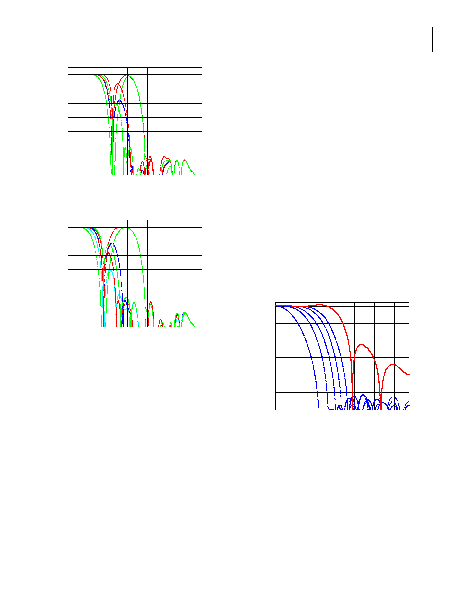
ADV7188
Rev. 0 | Page 31 of 112
0
10
20
30
40
50
60
70
0
10
8
6
4
2
12
05478-018
FREQUENCY (MHz)
COMBINED Y ANTIALIAS, PAL NOTCH FILTERS,
Y RESAMPLE
A
M
PLITU
D
E (
d
B
)
Figure 18. Y PAL Notch Filter Responses
0
10
20
30
40
50
60
70
0
10
8
6
4
2
12
05478-019
FREQUENCY (MHz)
COMBINED Y ANTIALIAS, NTSC NOTCH FILTERS,
Y RESAMPLE
AMP
L
ITUDE
(dB)
Figure 19. Y NTSC Notch Filter Responses
CHROMA FILTER
Data from the digital fine clamp block is processed by three sets
of filters. The data format at this point is CVBS for CVBS
inputs, chroma only for Y/C, or Cr/Cb interleaved for YPrPb
input formats.
·
Chroma Antialias Filter (CAA). The ADV7188 over-
samples the CVBS by a factor of 2 and the Chroma/CrCb
by a factor of 4. A decimating filter (CAA) is used to
preserve the active video band and to remove any out-of-
band components. The CAA filter has a fixed response.
·
Chroma Shaping Filters (CSH). The shaping filter block
(CSH) can be programmed to perform a variety of low-
pass responses. It can be used to selectively reduce the
bandwidth of the chroma signal for scaling or compression.
·
Digital Resampling Filter. This block is used to allow
dynamic resampling of the video signal to alter parameters
such as the time base of a line of video. Fundamentally, the
resampler is a set of low-pass filters. The actual response is
chosen by the system without user intervention.
The plots in Figure 20 show the overall response of all filters
together, from SH1 (narrowest) to SH5 (widest) in addition to
the wideband mode (in red).
0
10
20
30
40
50
60
0
5
4
3
2
1
6
05478-020
FREQUENCY (MHz)
COMBINED C ANTIALIAS, C SHAPING FILTER,
C RESAMPLER
ATTE
NUATION (dB)
Figure 20. Chroma Shaping Filter Responses
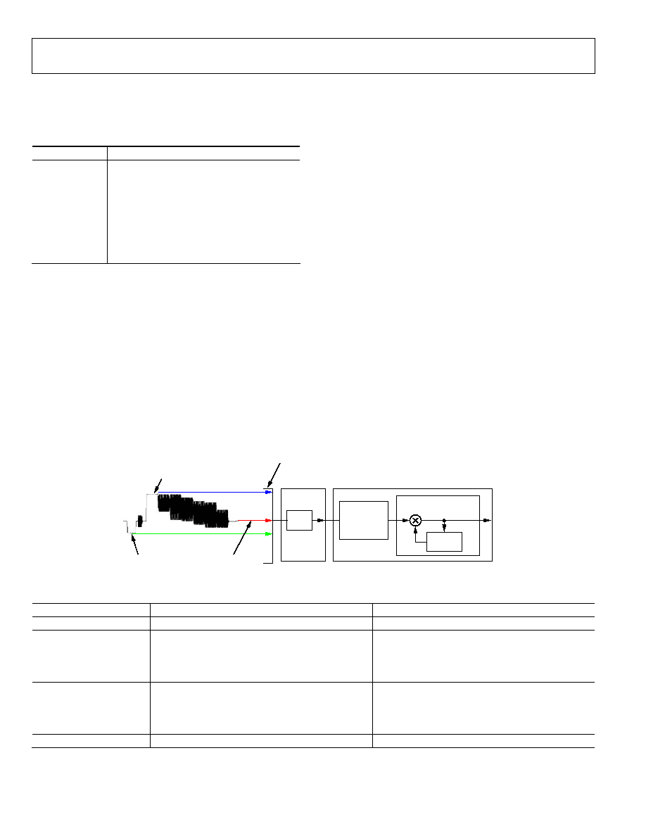
ADV7188
Rev. 0 | Page 32 of 112
CSFM[2:0] C-Shaping Filter Mode, Address 0x17 [7]
The C-shaping filter mode bits allow the user to select from a
range of low-pass filters for the chrominance signal.
Table 38. CSFM Function
CSFM[2:0] Description
000 (default)
1.5 MHz bandwidth filter
001
2.17 MHz bandwidth filter
010 SH1
011 SH2
100 SH3
101 SH4
110 SH5
111 Wideband
mode
GAIN OPERATION
The gain control within the ADV7188 is done on a purely
digital basis. The input ADCs support a 12-bit range, mapped
into a 1.6 V analog voltage range. Gain correction takes place
after the digitization in the form of a digital multiplier.
Advantages of this architecture over the commonly used PGA
(programmable gain amplifier) before the ADCs include that
the gain is now completely independent of supply, temperature,
and process variations.
As shown in Figure 21, the ADV7188 can decode a video signal
as long as it fits into the ADC window.
The two components to this are the amplitude of the input signal
and the dc level on which it resides. The dc level is set by the
clamping circuitry (see the Clamp Operation section).
If the amplitude of the analog video signal is too high, clipping
may occur resulting in visual artifacts. The analog input range
of the ADC, together with the clamp level, determines the
maximum supported amplitude of the video signal.
The minimum supported amplitude of the input video is
determined by the ADV7188's ability to retrieve horizontal and
vertical timing and to lock to the color burst, if present.
There are separate gain control units for luma and chroma data.
Both can operate independently of each other. The chroma unit,
however, can also take its gain value from the luma path.
The possible AGC modes are summarized in Table 39.
It is possible to freeze the automatic gain control loops. This
causes the loops to stop updating and the AGC-determined
gain at the time of the freeze to stay active until the loop is
either unfrozen or the gain mode of operation is changed.
The currently active gain from any of the modes can be read
back. Refer to the description of the dual-function manual gain
registers, LG[11:0] Luma Gain and CG[11:0] Chroma Gain, in
the Luma Gain and the Chroma Gain sections.
05478-021
ANALOG VOLTAGE
RANGE SUPPORTED BY ADC (1.6V RANGE FOR ADV7188)
DATA
PRE-
PROCESSOR
(DPP)
ADC
SDP
(GAIN SELECTION ONLY)
MAXIMUM
VOLTAGE
MINIMUM
VOLTAGE
CLAMP
LEVEL
GAIN
CONTROL
Figure 21. Gain Control Overview
Table 39. AGC Modes
Input Video Type
Luma Gain
Chroma Gain
Any
Manual gain luma.
Manual gain chroma.
Dependent on color burst amplitude.
Dependent on horizontal sync depth.
Taken from luma path.
Dependent on color burst amplitude.
CVBS
Peak white.
Taken from luma path.
Dependent on color burst amplitude.
Dependent on horizontal sync depth.
Taken from luma path.
Dependent on color burst amplitude.
Y/C
Peak white.
Taken from luma path.
YPrPb
Dependent on horizontal sync depth.
Taken from luma path.

ADV7188
Rev. 0 | Page 33 of 112
Luma Gain
LAGC[2:0] Luma Automatic Gain Control, Address 0x2C [6:4]
The luma automatic gain control mode bits select the mode of
operation for the gain control in the luma path.
There are ADI internal parameters to customize the peak white
gain control. Contact ADI for more information.
Table 40. LAGC Function
LAGC[2:0] Description
000
Manual fixed gain (use LMG[11:0])
001
AGC (blank level to sync tip); peak white algorithm
OFF
010
(default)
AGC (blank level to sync tip); peak white algorithm
ON
011 Reserved
100 Reserved
101 Reserved
110 Reserved
111 Freeze
gain
LAGT[1:0] Luma Automatic Gain Timing, Address 0x2F [7:6]
The luma automatic gain timing register allows the user to
influence the tracking speed of the luminance automatic gain
control. Note that this register only has an effect if the
LAGC[2:0] register is set to 001, 010, 011, or 100 (automatic
gain control modes).
If peak white AGC is enabled and active (see the STATUS_1[7:0]
Address 0x10 [7:0] section), the actual gain update speed is
dictated by the peak white AGC loop and, as a result, the LAGT
settings have no effect. As soon as the part leaves peak white
AGC, LAGT becomes relevant again.
The update speed for the peak white algorithm can be
customized by the use of internal parameters. Contact ADI for
more information.
Table 41. LAGT Function
LAGT[1:0] Description
00
Slow (TC = 2 sec)
01
Medium (TC = 1 sec)
10
Fast (TC = 0.2 sec)
11 (default)
Adaptive
LG[11:0] Luma Gain, Address 0x2F [3:0]; Address 0x30 [7:0];
LMG[11:0] Luma Manual Gain, Address 0x2F [3:0];
Address 0x30 [7:0]
Luma gain [11:0] is a dual-function register. If written to, a
desired manual luma gain can be programmed. This gain
becomes active if the LAGC[2:0] mode is switched to manual
fixed gain. Equation 2 and Equation 3 show how to calculate a
desired gain for NTSC and PAL standards, respectively.
NTSC Luma_Gain =
63
.
3
9078
.
0
1128
4095
]
0
:
11
[
1024
K
=
<LMG
(2)
PAL Luma_Gain =
351
.
3
838
.
0
1222
4095
]
0
:
11
[
1024
K
=
<LMG
(3)
If read back, this register returns the current gain value.
Depending on the setting in the LAGC[2:0] bits, this is one of
the following values:
·
Luma manual gain value (LAGC[2:0] set to luma manual
gain mode)
·
Luma automatic gain value (LAGC[2:0] set to any of the
automatic modes)
Table 42. LG/LMG Function
LG[11:0]/LMG[11:0] Read/Write Description
LMG[11:0] = X
Write
Manual gain for luma
path
LG[11:0]
Read
Actually used gain
For example, to program the ADV7188 into manual fixed gain
mode with a desired gain of 0.89 for the NTSC standard:
1.
Use Equation 2 to convert the gain:
0.95 × 1128 = 1071.6
2.
Truncate to integer value:
1071.6 = 1071
3.
Convert to hexadecimal:
1071d = 0x42F
4.
Split into two registers and program:
Luma Gain Control 1 [3:0] = 0x4
Luma Gain Control 2 [7:0] = 0x2F
5.
Enable manual fixed gain mode:
Set LAGC[2:0] to 000
BETACAM Enable Betacam Levels, Address 0x01 [5]
If YPrPb data is routed through the ADV7188, the automatic
gain control modes can target different video input levels, as
outlined in Table 45. Note that the BETACAM bit is valid only if
the input mode is YPrPb (component). The BETACAM bit sets
the target value for AGC operation. A review of the following
sections is useful.
·
INSEL[3:0] Input Selection, Address 0x00 [3:0] to find how
component video (YPrPb) can be routed through the
ADV7188.
·
Video Standard Selection to select the various standards,
for example, with and without pedestal.
The automatic gain control (AGC) algorithms adjust the levels
based on the setting of the BETACAM bit.
ADV7188
Rev. 0 | Page 34 of 112
Table 43. BETACAM Function
BETACAM Description
0 (default)
Assuming YPrPb is selected as input format.
Selecting PAL with pedestal selects MII.
Selecting PAL without pedestal selects SMPTE.
Selecting NTSC with pedestal selects MII.
Selecting NTSC without pedestal selects SMPTE.
1
Assuming YPrPb is selected as input format.
Selecting PAL with pedestal selects BETACAM.
Selecting PAL without pedestal selects BETACAM
variant.
Selecting NTSC with pedestal selects BETACAM.
Selecting NTSC without pedestal selects BETACAM
variant.
PW_UPD Peak White Update, Address 0x2B [0]
The peak white and average video algorithms determine the
gain based on measurements taken from the active video. The
PW_UPD bit determines the rate of gain change. LAGC[2:0]
must be set to the appropriate mode to enable the peak white or
average video mode in the first place.
For more information, refer to the LAGC[2:0] Luma Automatic
Gain Control, Address 0x2C [6:4] section.
0--Updates the gain once per video line.
1 (default)--Updates the gain once per field.
Chroma Gain
CAGC[1:0] Chroma Automatic Gain Control,
Address 0x2C [1:0]
These two bits select the basic mode of operation for automatic
gain control in the chroma path.
Table 44. CAGC Function
CAGC[1:0] Description
00
Manual fixed gain (use CMG[11:0]).
01
Use luma gain for chroma.
10 (default)
Automatic gain (based on color burst).
11 Freeze
chroma
gain.
Table 45. Betacam Levels
Name
Betacam (mV)
Betacam Variant (mV)
SMPTE (mV)
MII (mV)
Y Range
0 to 714 (incl. 7.5% pedestal)
0 to 714
0 to 700
0 to 700 (incl. 7.5% pedestal)
Pr and Pb Range
467 to +467
505 to +505
350 to +350
324 to +324
Sync Depth
286
286
300
300
CAGT[1:0] Chroma Automatic Gain Timing,
Address 0x2D [7:6]
This register allows the user to influence the tracking speed of
the chroma automatic gain control. It has an effect only if the
CAGC[1:0] register is set to 10 (automatic gain).
Table 46. CAGT Function
CAGT[1:0] Description
00
Slow (TC = 2 sec)
01
Medium (TC = 1 sec)
10
Fast (TC = 0.2 sec)
11 (default)
Adaptive
CG[11:0] Chroma Gain, Address 0x2D [3:0]; Address 0x2E
[7:0]; CMG[11:0] Chroma Manual Gain, Address 0x2D [3:0];
Address 0x2E [7:0]
CG[11:0] is a dual-function register. If written to, a desired
manual chroma gain can be programmed. This gain becomes
active if the CAGC[1:0] mode is switched to manual fixed gain.
Refer to Equation 4 for calculating a desired gain. If read back,
the register returns the current gain value. Depending on the
setting in the CAGC[1:0] bits, this is either
·
Chroma manual gain value (CAGC[1:0] set to chroma
manual gain mode)
·
Chroma automatic gain value (CAGC[1:0] set to any of the
automatic modes)
Table 47. CG/CMG Function
CG[11:0]/CMG[11:0] Read/Write Description
CMG[11:0] Write
Manual gain for chroma
path.
CG[11:0]
Read
Currently active gain.
(
)
4
...
0
1024
4095
0
_
=
<
=
CG
Gain
Chroma
(4)
For example, freezing the automatic gain loop and reading back
the CG[11:0] register results in a value of 0x47A.
1.
Convert the readback value to decimal:
0x47A = 1146d
2.
Apply Equation 4 to convert the readback value:
1146/1024 = 1.12
CKE Color Kill Enable, Address 0x2B [6]
This bit allows the optional color kill function to be switched on
or off. For QAM-based video standards (PAL and NTSC) and
FM-based systems (SECAM), the threshold for the color kill
decision is selectable via the CKILLTHR[2:0] bits.
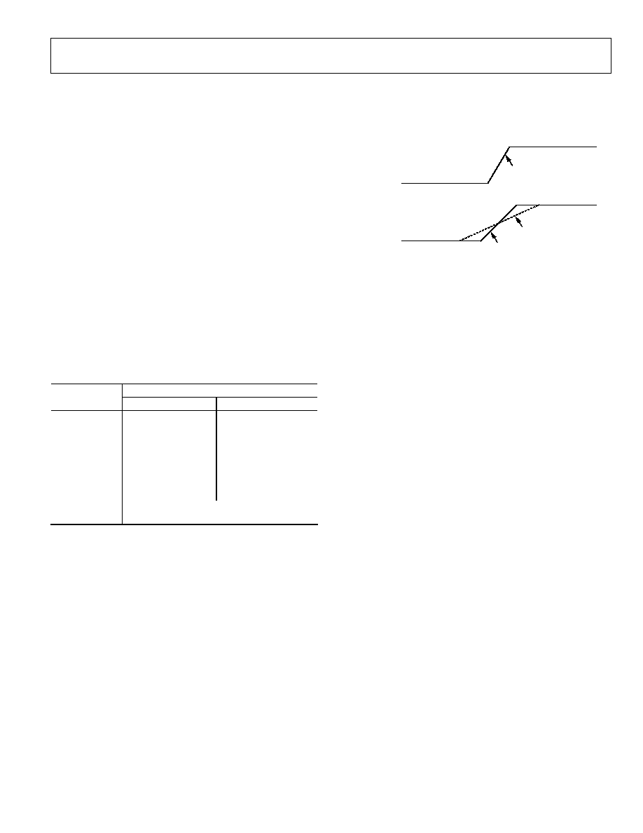
ADV7188
Rev. 0 | Page 35 of 112
If color kill is enabled, and if the color carrier of the incoming
video signal is less than the threshold for 128 consecutive video
lines, color processing is switched off (black and white output).
To switch the color processing back on, another 128 consecutive
lines with a color burst greater than the threshold are required.
The color kill option works only for input signals with a modu-
lated chroma part. For component input (YPrPb), there is no
color kill.
0--Disables color kill.
1 (default)--Enables color kill.
CKILLTHR[2:0] Color Kill Threshold, Address 0x3D [6:4]
The CKILLTHR[2:0] bits allow the user to select a threshold for
the color kill function. The threshold applies only to QAM-
based (NTSC and PAL) or FM-modulated (SECAM) video
standards.
To enable the color kill function, the CKE bit must be set. For
settings 000, 001, 010, and 011, chroma demodulation inside
the ADV7188 may not work satisfactorily for poor input video
signals.
Table 48. CKILLTHR Function
Description
CKILLTHR[2:0]
SECAM NTSC,
PAL
000
No color kill
Kill at < 0.5%
001
Kill at < 5%
Kill at < 1.5%
010
Kill at < 7%
Kill at < 2.5%
011
Kill at < 8%
Kill at < 4.0%
100 (default)
Kill at < 9.5%
Kill at < 8.5%
101
Kill at < 15%
Kill at < 16.0%
110
Kill at < 32%
Kill at < 32.0%.
111
Reserved for ADI internal use only; do not
select
CHROMA TRANSIENT IMPROVEMENT (CTI)
The signal bandwidth allocated for chroma is typically much
smaller than that of luminance. In the past, this was a valid way
to fit a color video signal into a given overall bandwidth because
the human eye is less sensitive to chrominance than to
luminance.
The uneven bandwidth, however, may lead to visual artifacts in
sharp color transitions. At the border of two bars of color, both
components (luma and chroma) change at the same time (see
Figure 22).
Due to the higher bandwidth, the signal transition of the luma
component is usually much sharper than that of the chroma
component. The color edge is not sharp but blurred, in the
worst case over several pixels.
05478-022
LUMA
SIGNAL
DEMODULATED
CHROMA
SIGNAL
LUMA SIGNAL WITH A
TRANSITION, ACCOMPANIED
BY A CHROMA TRANSITION
ORIGINAL, "SLOW" CHROMA
TRANSITION PRIOR TO CTI
SHARPENED CHROMA
TRANSITION AT THE
OUTPUT OF CTI
Figure 22. CTI Luma/Chroma Transition
The CTI block examines the input video data. It detects
transitions of chroma, and can be programmed to steepen the
chroma edges in an attempt to artificially restore lost color
bandwidth. However, it operates only on edges above a certain
threshold to ensure that noise is not emphasized. Care has also
been taken to avoid edge ringing and undesirable saturation
and hue distortion.
Chroma transient improvements are needed primarily for
signals that experienced severe chroma bandwidth limitations.
For those types of signals, it is strongly recommended to enable
the CTI block via CTI_EN.
CTI_EN Chroma Transient Improvement Enable,
Address 0x4D [0]
0--Disables the CTI block.
1 (default)--Enables the CTI block.
CTI_AB_EN Chroma Transient Improvement
Alpha Blend Enable, Address 0x4D [1]
This bit enables an alpha-blend function, which mixes the
transient improved chroma with the original signal. The
sharpness of the alpha blending can be configured via the
CTI_AB[1:0] bits. For the alpha blender to be active, the CTI
block must be enabled via the CTI_EN bit.
0--Disables the CTI alpha blender.
1 (default)--Enables the CTI alpha blender.
CTI_AB[1:0] Chroma Transient Improvement Alpha Blend,
Address 0x4D [3:2]
This controls the behavior of alpha-blend circuitry that mixes
the sharpened chroma signal with the original one. It thereby
controls the visual impact of CTI on the output data.
For CTI_AB[1:0] to become active, the CTI block must be
enabled via the CTI_EN bit, and the alpha blender must be
switched on via CTI_AB_EN.
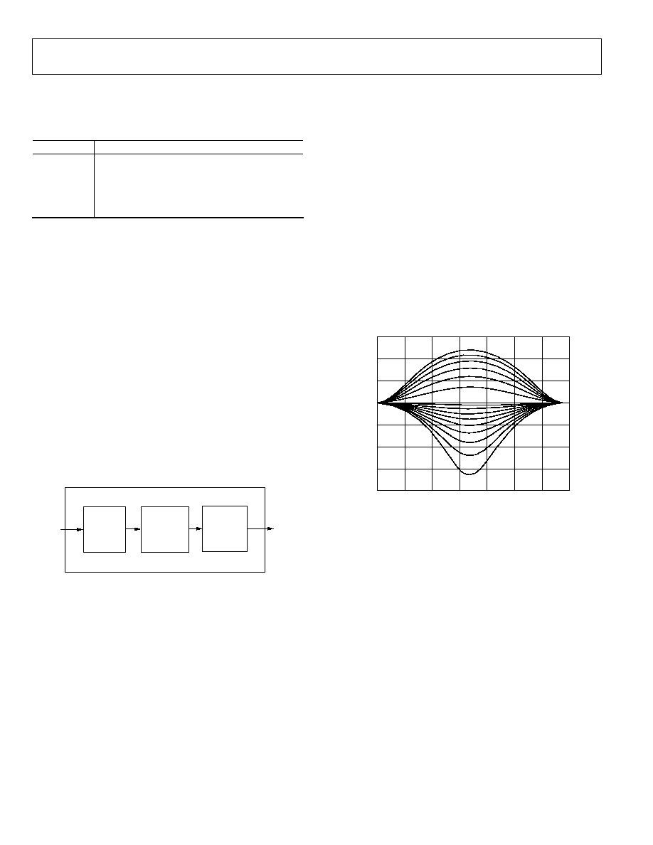
ADV7188
Rev. 0 | Page 36 of 112
Sharp blending maximizes the effect of CTI on the picture, but
may also increase the visual impact of small amplitude, high
frequency chroma noise.
Table 49. CTI_AB Function
CTI_AB[1:0] Description
00
Sharpest mixing between sharpened and original
chroma signal
01 Sharp
mixing
10 Smooth
mixing
11 (default)
Smoothest alpha blend function
CTI_C_TH[7:0] CTI Chroma Threshold, Address 0x4E [7:0]
The CTI_C_TH[7:0] value is an unsigned, 8-bit number speci-
fying how big the amplitude step in a chroma transition has to
be in order to be steepened by the CTI block. Programming a
small value into this register causes even smaller edges to be
steepened by the CTI block. Making CTI_C_TH[7:0] a large
value causes the block to improve large transitions only.
The default value for CTI_C_TH[7:0] is 0x08, indicating the
threshold for the chroma edges prior to CTI.
DIGITAL NOISE REDUCTION (DNR), AND LUMA
PEAKING FILTER
DNR is based on the assumption that high frequency signals
with low amplitude are probably noise and therefore that their
removal improves picture quality. There are two DNR blocks in
the ADV7188: the DNR1 block before the luma peaking filter
and the DNR2 block after the luma peaking filter, as shown in
Figure 23.
LUMA
OUTPUT
DNR1
LUMA PEAKING
FILTER
DNR2
LUMA
SIGNAL
05478-
023
Figure 23. DNR and Peaking Block Diagram
DNR_EN Digital Noise Reduction Enable, Address 0x4D [5]
0--Bypasses DNR (disables it).
1 (default)--Enables DNR on the luma data.
DNR_TH[7:0] DNR Noise Threshold, Address 0x50 [7:0]
The DNR1 block is positioned before the luma peaking block.
The DNR_TH[7:0] value is an unsigned 8-bit number that
determines the maximum edge that is still interpreted as noise
and, therefore, blanked from the luma data. Programming a
large value into DNR_TH[7:0] causes the DNR block to
interpret even large transients as noise and removes them. As a
result, the effect on the video data is more visible.
Programming a small value causes only small transients to be
seen as noise and to be removed.
The recommended DNR_TH[7:0] setting for A/V inputs is
0x04, and the recommended DNR_TH[7:0] setting for tuner
inputs is 0x0A.
The default value for DNR_TH[7:0] is 0x08, indicating the
threshold for maximum luma edges to be interpreted as noise.
PEAKING_GAIN[7:0], Luma Peaking Gain, Address 0xFB [7:0]
This filter can be manually enabled. The user can boost or
attenuate the mid region of the Y spectrum around 3 MHz. The
peaking filter can visually improve the picture by showing more
definition on the picture details that contain frequency
components around 3 MHz. The default value (0x40) in this
register passes through the luma data unaltered (0 dB response).
A lower value attenuates the signal and a higher value amplifies
it. A plot of the filter responses is shown in Figure 24.
15
20
0
7
05478-024
FREQUENCY (MHz)
FILTER
R
ESPON
SE (
d
B
)
10
5
0
5
10
15
1
2
3
4
5
6
PEAKING GAIN USING BP FILTER
Figure 24. Peaking Filter Responses
DNR_TH2[7:0] DNR Noise Threshold 2, Address 0xFC [7:0]
The DNR2 block is positioned after the luma peaking block, so
it affects the amplified luma signal. It operates in the same way
as the DNR1 block but has an independent threshold control,
DNR_TH2[7:0]. This value is an unsigned 8-bit number, that
determines the maximum edge that is still interpreted as noise
and, therefore, blanked from the luma data. Programming a
large value into DNR_TH2[7:0] causes the DNR block to
interpret even large transients as noise and remove them. As a
result, the effect on the video data is more visible. Programming
a small value causes only small transients to be seen as noise
and removed.

ADV7188
Rev. 0 | Page 37 of 112
COMB FILTERS
The comb filters of the ADV7188 have been greatly improved to
automatically handle video of all types, standards, and levels of
quality. The NTSC and PAL configuration registers allow the
user to customize comb filter operation, depending on which
video standard is detected (by autodetection) or selected (by
manual programming). In addition to the bits listed in this
section, there are some other ADI internal controls; contact
ADI for more information.
NTSC Comb Filter Settings
Used for NTSC-M/J CVBS inputs.
NSFSEL[1:0] Split Filter Selection NTSC, Address 0x19 [3:2]
NSFSEL[1:0] selects how much of the overall signal bandwidth
is fed to the combs. A narrow bandwidth split filter gives better
performance on diagonal lines, but leaves more dot crawl in the
final output image. The opposite is true for a wide bandwidth
split filter.
Table 50. NSFSEL Function
NSFSEL[1:0] Description
00 (default)
Narrow
01 Medium
10
Medium
11 Wide
CTAPSN[1:0] Chroma Comb Taps NTSC, Address 0x38 [7:6]
Table 51. CTAPSN Function
CTAPSN[1:0] Description
00
Do not use
01
NTSC chroma comb adapts 3 lines (3 taps) to
2 lines (2 taps)
10 (default)
NTSC chroma comb adapts 5 lines (5 taps) to
3 lines (3 taps)
11
NTSC chroma comb adapts 5 lines (5 taps) to
4 lines (4 taps)
CCMN[2:0] Chroma Comb Mode NTSC, Address 0x38 [5:3]
See Table 52.
YCMN[2:0] Luma Comb Mode NTSC, Address 0x38 [2:0]
See Table 53.
Table 52. CCMN Function
CCMN[2:0]
Description
Configuration
Adaptive 3-line chroma comb for CTAPSN = 01
Adaptive 4-line chroma comb for CTAPSN = 10
000 (default)
Adaptive comb mode
Adaptive 5-line chroma comb for CTAPSN = 11
100
Disable chroma comb
Fixed 2-line chroma comb for CTAPSN = 01
Fixed 3-line chroma comb for CTAPSN = 10
101
Fixed chroma comb (top lines of line memory)
Fixed 4-line chroma comb for CTAPSN = 11
Fixed 3-line chroma comb for CTAPSN = 01
Fixed 4-line chroma comb for CTAPSN = 10
110
Fixed chroma comb (all lines of line memory)
Fixed 5-line chroma comb for CTAPSN = 11
Fixed 2-line chroma comb for CTAPSN = 01
Fixed 3-line chroma comb for CTAPSN = 10
111
Fixed chroma comb (bottom lines of line memory)
Fixed 4-line chroma comb for CTAPSN = 11
Table 53.YCMN Function
YCMN[2:0] Description
Configuration
000 (default)
Adaptive comb mode
Adaptive 3-line (3 taps) luma comb
100
Disable luma comb
Use low-pass/notch filter; see the Y-Shaping Filter section
101
Fixed luma comb (top lines of line memory)
Fixed 2-line (2 taps) luma comb
110
Fixed luma comb (all lines of line memory)
Fixed 3-line (3 taps) luma comb
111
Fixed luma comb (bottom lines of line memory)
Fixed 2-line (2 taps) luma comb

ADV7188
Rev. 0 | Page 38 of 112
PAL Comb Filter Settings
Used for PAL-B/G/H/I/D, PAL-M, PAL-Combinational N,
PAL-60 and NTSC-443 CVBS inputs.
PSFSEL[1:0] Split Filter Selection PAL, Address 0x19 [1:0]
PFSEL[1:0] selects how much of the overall signal bandwidth is
fed to the combs. A wide bandwidth split filter eliminates dot
crawl, but shows imperfections on diagonal lines. The opposite
is true for a narrow bandwidth split filter.
Table 54. PSFSEL Function
PSFSEL[1:0] Description
00
Narrow
01 (default)
Medium
10
Wide
11 Widest
CTAPSP[1:0] Chroma Comb Taps PAL, Address 0x39 [7:6]
Table 55. CTAPSP Function
CTAPSP[1:0] Description
00
Do not use.
01
PAL chroma comb adapts 5 lines (3 taps) to
3 lines (2 taps); cancels cross luma only.
10
PAL chroma comb adapts 5 lines (5 taps) to
3 lines (3 taps); cancels cross luma and hue error
less well.
11 (default)
PAL chroma comb adapts 5 lines (5 taps) to
4 lines (4 taps); cancels cross luma and hue error
well.
CCMP[2:0] Chroma Comb Mode PAL, Address 0x39 [5:3]
See Table 56.
YCMP[2:0] Luma Comb Mode PAL, Address 0x39 [2:0]
See Table 57.
Vertical Blank Control
Each vertical blank control register has the same meaning for
the following bits:
00--Early by 1 line.
10--Delay by 1 line.
11--Delay by 2 lines.
01 (default) is described under each register.
NVBIOLCM[1:0] NTSC VBI Odd Field Luma Comb Mode,
Address 0xEB [7:6]
These bits control the first combed line after VBI on NTSC odd
field (luma comb).
01 (default)--SMPTE170 compliant, blank lines 1 to 20, 264 to
282, comb half lines.
NVBIELCM[1:0] NTSC VBI Even Field Luma Comb Mode,
Address 0xEB [5:4]
These bits control the first combed line after VBI on NTSC
even field (luma comb).
01 (default)--SMPTE170 compliant, blank lines 1 to 20, 264 to
282, comb half lines.
PVBIOLCM[1:0] PAL VBI Odd Field Luma Comb Mode,
Address 0xEB [3:2]
These bits control the first combed line after VBI on PAL odd
field (luma comb).
01 (default)--BT470 compliant, blank lines 624 to 22, 311 to
335, comb half lines.
PVBIELCM[1:0] PAL VBI Even Field Luma Comb Mode,
Address 0xEB [1:0]
These bits control the first combed line after VBI on PAL even
field (luma comb).
01 (default)--BT470 compliant, blank lines 624 to 22, 311 to
335, comb half lines.
NVBIOCCM[1:0] NTSC VBI Odd Field Chroma Comb
Mode, Address 0xEC [7:6]
These bits control the first combed line after VBI on NTSC odd
field (chroma comb).
01 (default)--SMPTE170 compliant, no color on lines 1 to 20,
264 to 282, chroma present on half lines.
NVBIECCM[1:0] NTSC VBI Even Field Chroma Comb
Mode, Address 0xEC [5:4]
These bits control the first combed line after VBI on NTSC
even field (chroma comb).
01 (default)--SMPTE170 compliant, no color on lines 1 to 20,
264 to 282, chroma present on half lines.
PVBIOCCM[1:0] PAL VBI Odd Field Chroma Comb Mode,
Address 0xEC [3:2]
These bits control the first combed line after VBI on PAL odd
field (chroma comb).
01 (default)--BT470 compliant, no color on lines 624 to 22, 311
to 335, chroma present on half lines.
PVBIECCM[1:0] PAL VBI Even Field Chroma Comb Mode,
Address 0xEC [1:0]
These bits control the first combed line after VBI on PAL even
field (chroma comb).
01 (default)--BT470 compliant, no color on lines 624 to 22, 311
to 335, chroma present on half lines.

ADV7188
Rev. 0 | Page 39 of 112
Table 56. CCMP Function
CCMP[2:0] Description
Configuration
Adaptive 3-line chroma comb for CTAPSP = 01.
Adaptive 4-line chroma comb for CTAPSP = 10.
000 (default)
Adaptive comb mode.
Adaptive 5-line chroma comb for CTAPSP = 11.
100
Disable chroma comb.
Fixed 2-line chroma comb for CTAPSP = 01.
Fixed 3-line chroma comb for CTAPSP = 10.
101
Fixed chroma comb (top lines of line memory).
Fixed 4-line chroma comb for CTAPSP = 11.
Fixed 3-line chroma comb for CTAPSP = 01.
Fixed 4-line chroma comb for CTAPSP = 10.
110
Fixed chroma comb (all lines of line memory).
Fixed 5-line chroma comb for CTAPSP = 11.
Fixed 2-line chroma comb for CTAPSP = 01.
Fixed 3-line chroma comb for CTAPSP = 10.
111
Fixed chroma comb (bottom lines of line memory).
Fixed 4-line chroma comb for CTAPSP = 11.
Table 57. YCMP Function
YCMP[2:0] Description
Configuration
0xx (default)
Adaptive comb mode.
Adaptive 5 lines (3 taps) luma comb.
100
Disable luma comb.
Use low-pass/notch filter; see the Y-Shaping Filter section.
101
Fixed luma comb (top lines of line memory).
Fixed 3 lines (2 taps) luma comb.
110
Fixed luma comb (all lines of line memory).
Fixed 5 lines (3 taps) luma comb.
111
Fixed luma comb (bottom lines of line memory).
Fixed 3 lines (2 taps) luma comb.
AV CODE INSERTION AND CONTROLS
This section describes the I
2
C-based controls that affect
·
Insertion of AV codes into the data stream.
·
Data blanking during the vertical blank interval (VBI).
·
The range of data values permitted in the output data
stream.
·
The relative delay of luma vs. chroma signals.
Note that some of the decoded VBI data is being inserted
during the horizontal blanking interval. See the Gemstar Data
Recovery section for more information.
BT656-4 ITU Standard BT-R.656-4 Enable, Address 0x04 [7]
The ITU has changed the position for toggling the V bit within
the SAV EAV codes for NTSC between revisions 3 and 4. The
BT656-4 standard bit allows the user to select an output mode
that is compliant with either the previous or the new standard.
For more information, review the standard at http://www.itu.int.
Note that the standard change affects NTSC only and has no
bearing on PAL.
0 (default)--The BT656-3 specification is used. The V bit goes
low at EAV of Lines 10 and 273.
1--The BT656-4 specification is used. The V bit goes low at
EAV of Lines 20 and 283.
SD_DUP_AV Duplicate AV Codes, Address 0x03 [0]
Depending on the output interface width, it may be necessary to
duplicate the AV codes from the luma path into the chroma path.
In an 8-/10-bit-wide output interface (Cb/Y/Cr/Y interleaved
data), the AV codes are defined as FF/00/00/AV, with AV being
the transmitted word that contains information about H/V/F.
In this output interface mode, the following assignment takes
place: Cb = FF, Y = 00, Cr = 00, and Y = AV.
In a 16-/20-bit output interface where Y and Cr/Cb are delivered
via separate data buses, the AV code is over the whole 16/20
bits. The SD_DUP_AV bit allows the user to replicate the AV
codes on both buses, so the full AV sequence can be found on
the Y bus and on the Cr/Cb bus. See Figure 25.
0 (default)--The AV codes are in single fashion (to suit 8/10 bit
interleaved data output).
1--The AV codes are duplicated (for 16-/20-bit interfaces).
VBI_EN Vertical Blanking Interval Data Enable,
Address 0x03 [7]
The VBI enable bit allows data such as intercast and closed
caption data to be passed through the luma channel of the
decoder with a minimal amount of filtering. All data for Line 1
to Line 21 is passed through and available at the output port.
The ADV7188 does not blank the luma data, and automatically
switches all filters along the luma data path into their widest
bandwidth. For active video, the filter settings for YSH and YPK
are restored.
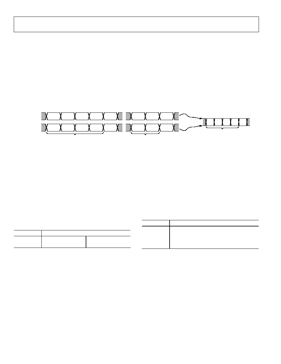
ADV7188
Rev. 0 | Page 40 of 112
Refer to the BL_C_VBI Blank Chroma during VBI, Address
0x04 [2] section for information on the chroma path.
0 (default)--All video lines are filtered/scaled.
1--Only the active video region is filtered/scaled.
BL_C_VBI Blank Chroma during VBI, Address 0x04 [2]
When BL_C_VBI is set high, the Cr and Cb values of all VBI
lines are blanked.
This is done so any data that may arrive during VBI is not
decoded as color and output through Cr and Cb. As a result, it
is possible to send VBI lines into the decoder, then output them
through an encoder again, undistorted. Without this blanking,
any wrongly decoded color is encoded by the video encoder;
therefore, the VBI lines are distorted.
0--Decodes and outputs color during VBI.
1 (default)--Blanks Cr and Cb values during VBI.
05478-025
Y DATA BUS
00
AV
Y
FF
00
00
AV
Y
FF
Cr/Cb DATA BUS
00
00
AV
Cb
FF
00
Cb
AV CODE SECTION
AV CODE SECTION
FF
00
00
AV
Cb
AV CODE SECTION
Cb/Y/Cr/Y
INTERLEAVED
8-/10-BIT INTERFACE
16-/20-BIT INTERFACE
16-/20-BIT INTERFACE
SD_DUP_AV = 1
SD_DUP_AV = 0
Figure 25. AV Code Duplication Control
RANGE Range Selection, Address 0x04 [0]
AV codes (as per ITU-R BT-656, formerly known as CCIR-656)
consist of a fixed header made up of 0xFF and 0x00 values.
These two values are reserved and therefore not to be used for
active video. Additionally, the ITU specifies that the nominal
range for video should be restricted to values between 16 and
235 for luma and 16 to 240 for chroma.
The RANGE bit allows the user to limit the range of values
output by the ADV7188 to the recommended value range. In
any case, it ensures that the reserved values of 255d (0xFF) and
00d (0x00) are not presented on the output pins unless they are
part of an AV code header.
Table 58. RANGE Function
RANGE Description
0
16 Y 235
16 C 240
1 (default)
1 Y 254
1 C 254
AUTO_PDC_EN Automatic Programmed Delay Control,
Address 0x27 [6]
Enabling the AUTO_PDC_EN function activates a function
within the ADV7188 that automatically programs LTA[1:0] and
CTA[2:0] to have the chroma and luma data match delays for all
modes of operation.
0--The ADV7188 uses the LTA[1:0] and CTA[2:0] values for
delaying luma and chroma samples. Refer to the LTA[1:0] Luma
Timing Adjust, Address 0x27 [1:0] and the CTA[2:0] Chroma
Timing Adjust, Address 0x27 [5:3] sections.
1 (default)--The ADV7188 automatically programs the LTA
and CTA values to have luma and chroma aligned at the output.
Manual registers LTA[1:0] and CTA[2:0] are not used.
LTA[1:0] Luma Timing Adjust, Address 0x27 [1:0]
This register allows the user to specify a timing difference
between chroma and luma samples.
Note that there is a certain functionality overlap with the
CTA[2:0] register. For manual programming, use the following
defaults:
·
CVBS input LTA[1:0] = 00
·
YC input LTA[1:0] = 01
·
YPrPb input LTA[1:0] =01
Table 59. LTA Function
LTA[1:0] Description
00 (default)
No delay.
01
Luma 1 clk (37 ns) delayed.
10
Luma 2 clk (74 ns) early.
11
Luma 1 clk (37 ns) early.
CTA[2:0] Chroma Timing Adjust, Address 0x27 [5:3]
This register allows the user to specify a timing difference
between chroma and luma samples. This may be used to
compensate for external filter group delay differences in the
luma vs. chroma path, and to allow a different number of
pipeline delays while processing the video downstream. Review
this functionality together with the LTA[1:0] register.
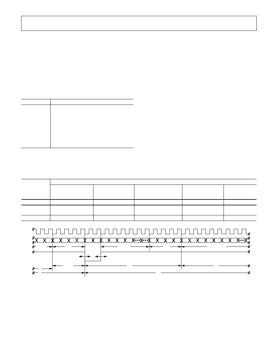
ADV7188
Rev. 0 | Page 41 of 112
The chroma can be delayed/advanced only in chroma pixel
steps. One chroma pixel step is equal to two luma pixels. The
programmable delay occurs after demodulation, where one can
no longer delay by luma pixel steps.
For manual programming, use the following defaults:
·
CVBS input CTA[2:0] = 011
·
YC input CTA[2:0] = 101
·
YPrPb input CTA[2:0] =110
Table 60. CTA Function
CTA[2:0] Description
000
Not used.
001
Chroma + 2 chroma pixel (early).
010
Chroma + 1 chroma pixel (early).
011 (default)
No delay.
100
Chroma 1 chroma pixel (late).
101
Chroma 2 chroma pixel (late).
110
Chroma 3 chroma pixel (late).
111 Not
used.
SYNCHRONIZATION OUTPUT SIGNALS
HS Configuration
The following controls allow the user to configure the behavior
of the HS output pin only:
·
Beginning of HS signal via HSB[10:0]
·
End of HS signal via HSE[10:0]
·
Polarity of HS using PHS
The HS begin and HS end registers allow the user to freely
position the HS output (pin) within the video line. The values
in HSB[10:0] and HSE[10:0] are measured in pixel units from
the falling edge of HS. Using both values, the user can program
both the position and length of the HS output signal.
HSB[10:0] HS Begin, Address 0x34 [6:4], Address 0x35 [7:0]
The position of this edge is controlled by placing a binary
number into HSB[10:0]. The number applied offsets the edge
with respect to an internal counter that is reset to 0 immediately
after EAV code FF, 00, 00, XY (see Figure 26). HSB[10:0] is set
to 00000000010, which is 2 LLC1 clock cycles from count[0].
The default value of HSB[10:0] is 0x002, indicating that the HS
pulse starts two pixels after the falling edge of HS.
.
Table 61. HS Timing Parameters (see Figure 26)
Characteristic
Standard
HS Begin Adjust
(HSB[10:0]) (default)
HS End Adjust
(HSE[10:0]) (default)
HS to Active Video
(LLC1 Clock Cycles)
(C in Figure 26) (default)
Active Video
Samples/Line
(D in)
Total LLC1
Clock Cycles
(E in)
NTSC
00000000010
00000000000
272
720Y + 720C = 1440
1716
NTSC Square
Pixel
00000000010
00000000000
276
640Y + 640C = 1280
1560
PAL
00000000010
00000000000
284
720Y + 720C = 1440
1728
05478-026
E
ACTIVE
VIDEO
LLC1
PIXEL
BUS
HS
Cr
Y
FF
00
00
XY
80
10
80
10
80
10
FF
00
00
XY
Cb
Y
Cr
Y
Cb
Y
Cr
4 LLC1
D
HSB[10:0]
HSE[10:0]
C
E
D
SAV
ACTIVE VIDEO
H BLANK
EAV
Figure 26. HS Timing
HSE[10:0] HS End, Address 0x34 [2:0], Address 0x36 [7:0]
The position of this edge is controlled by placing a binary
number into HSE[10:0]. The number applied offsets the edge
with respect to an internal counter that is reset to 0 immediately
after EAV code FF, 00, 00, XY (see Figure 26). HSE is set to
00000000000, which is 0 LLC1 clock cycles from count[0].
The default value of HSE[10:0] is 000, indicating that the HS
pulse ends 0 pixels after falling edge of HS.

ADV7188
Rev. 0 | Page 42 of 112
For example
1.
To shift the HS toward active video by 20 LLC1s, add 20
LLC1s to both HSB and HSE, that is HSB[10:0] =
[00000010110], HSE[10:0] = [00000010100]
2.
To shift the HS away from active video by 20 LLC1s, add 1696
LLC1s to both HSB and HSE (for NTSC), that is, HSB[10:0] =
[11010100010], HSE[10:0] = [11010100000]. 1696 is derived
from the NTSC total number of pixels = 1716.
To move 20 LLC1s away from active video is equal to subtracting
20 from 1716 and adding the result in binary to both HSB[10:0]
and HSE[10:0].
PHS Polarity HS, Address 0x37 [7]
The polarity of the HS pin can be inverted using the PHS bit.
0 (default)--HS is active high.
1--HS is active low.
VS and FIELD Configuration
The following controls allow the user to configure the behavior
of the VS and FIELD output pins, and to generate embedded AV
codes:
·
ADV encoder-compatible signals via NEWAVMODE
·
PVS, PF
·
HVSTIM
·
VSBHO, VSBHE
·
VSEHO, VSEHE
·
For NTSC control:
o
NVBEGDELO, NVBEGDELE, NVBEGSIGN,
NVBEG[4:0]
o
NVENDDELO, NVENDDELE, NVENDSIGN,
NVEND[4:0]
o
NFTOGDELO, NFTOGDELE, NFTOGSIGN,
NFTOG[4:0]
·
For PAL control:
o
PVBEGDELO, PVBEGDELE, PVBEGSIGN, PVBEG[4:0]
o
PVENDDELO, PVENDDELE, PVENDSIGN,
PVEND[4:0]
o
PFTOGDELO, PFTOGDELE, PFTOGSIGN, PFTOG[4:0]
NEWAVMODE New AV Mode, Address 0x31 [4]
0--EAV/SAV codes are generated to suit ADI encoders. No
adjustments are possible.
1 (default)--Enables the manual position of the VSYNC, Field,
and AV codes using Register 0x34 to Register 0x37 and Register
0xE5 to Register 0xEA. Default register settings are CCIR656
compliant; see Figure 27 for NTSC and Figure 32 for PAL. For
recommended manual user settings, see Table 62 and Figure 28
for NTSC; see Table 63 and Figure 33 for PAL.
HVSTIM Horizontal VS Timing, Address 0x31 [3]
The HVSTIM bit allows the user to select where the VS signal is
being asserted within a line of video. Some interface circuitry
may require VS to go low while HS is low.
0 (default)--The start of the line is relative to HSE.
1--The start of the line is relative to HSB.
VSBHO VS Begin Horizontal Position Odd, Address 0x32 [7]
This bit selects the position within a line at which the VS pin
(not the bit in the AV code) becomes active. Some follow-on
chips require the VS pin to change state only when HS is
high/low.
0 (default)--The VS pin goes high at the middle of a line of
video (odd field).
1--The VS pin changes state at the start of a line (odd field).
VSBHE VS Begin Horizontal Position Even, Address 0x32 [6]
This bit selects the position within a line at which the VS pin
(not the bit in the AV code) becomes active. Some follow-on
chips require the VS pin to change state only when HS is
high/low.
0--The VS pin goes high at the middle of a line of video (even
field).
1 (default)--The VS pin changes state at the start of a line (even
field).
VSEHO VS End Horizontal Position Odd, Address 0x33 [7]
This bit selects the position within a line at which the VS pin
(not the bit in the AV code) becomes inactive. Some follow-on
chips require the VS pin to change state only when HS is
high/low.
0--The VS pin goes low (inactive) at the middle of a line of
video (odd field).
1 (default)--The VS pin changes state at the start of a line (odd
field).
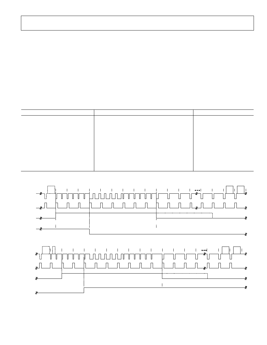
ADV7188
Rev. 0 | Page 43 of 112
VSEHE VS End Horizontal Position Even, Address 0x33 [6]
This bit selects the position within a line at which the VS pin
(not the bit in the AV code) becomes inactive. Some follow-on
chips require the VS pin to change state only when HS is
high/low.
0 (default)--The VS pin goes low (inactive) at the middle of a
line of video (even field).
1--The VS pin changes state at the start of a line (even field).
PVS Polarity VS, Address 0x37 [5]
The polarity of the VS pin can be inverted using the PVS bit.
0 (default)--VS is active high.
1--VS is active low.
PF Polarity FIELD, Address 0x37 [3]
The polarity of the FIELD pin can be inverted using the PF bit.
0 (default)--FIELD is active high.
1--FIELD is active low.
Table 62. Recommended User Settings for NTSC (See Figure 28)
Register Register
Name
Write
0x31
VSYNC Field Control 1
0x1A
0x32
VSYNC Field Control 2
0x81
0x33
VSYNC Field Control 3
0x84
0x34
HSYNC Position 1
0x00
0x35
HSYNC Position 2
0x00
0x36
HSYNC Position 3
0x7D
0x37 POLARITY
0xA1
0xE5 NTSV_V_BIT_BEG
0x41
0xE6 NTSC_V_BIT_END
0x84
0xE7 NTSC_F_BIT_TOG
0x06
05478-
027
OUTPUT
VIDEO
FIELD 1
FIELD 2
H
V
F
OUTPUT
VIDEO
H
V
F
525
1
2
3
4
5
6
7
8
9
10
11
12
13
19
20
21
22
NVBEG[4:0] = 0x5
NVBEG[4:0] = 0x5
NVEND[4:0] = 0x4
NVEND[4:0] = 0x4
NFTOG[4:0] = 0x3
NFTOG[4:0] = 0x3
*BT.656-4
REG 0x04, BIT 7 = 1
*BT.656-4
REG 0x04, BIT 7 = 1
*APPLIES IF NEMAVMODE = 0:
MUST BE MANUALLY SHIFTED IF NEWAVMODE = 1.
262
263
264
265
266
267
268
269
270
271
272
273
274
275
276
283
284
285
Figure 27. NTSC Default (BT.656). The Polarity of H, V, and F is Embedded in the Data.
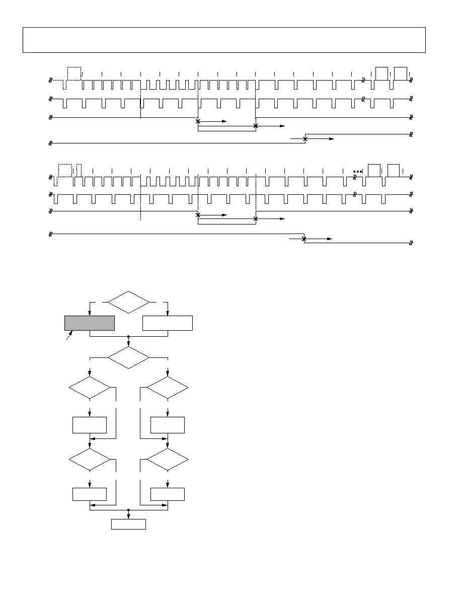
ADV7188
Rev. 0 | Page 44 of 112
NVBEG[4:0] =0x0
NVEND[4:0] = 0x3
05478-
028
FIELD 1
OUTPUT
VIDEO
FIELD
OUTPUT
HS
OUTPUT
NFTOG[4:0] = 0x5
VS
OUTPUT
525
1
2
3
4
5
6
7
8
9
10
11
12
13
14
15
21
22
FIELD 2
OUTPUT
VIDEO
FIELD
OUTPUT
HS
OUTPUT
VS
OUTPUT
262
263
264
265
266
267
268
269
270
271
272
273
274
275
276
277
284
285
NVBEG[4:0] = 0x0
NVEND[4:0] = 0x3
NFTOG[4:0] = 0x5
Figure 28. NTSC Typical VSYNC/Field Positions Using Register Writes in Table 62
05478-029
ADVANCE BEGIN OF
VSYNC BY NVBEG[4:0]
DELAY BEGIN OF
VSYNC BY NVBEG[4:0]
VSYNC BEGIN
NVBEGSIGN
ODD FIELD?
0
1
NO
YES
NVBEGDELO
VSBHO
ADDITIONAL
DELAY BY
1 LINE
ADVANCE BY
0.5 LINE
1
0
1
0
NVBEGDELE
VSBHE
ADDITIONAL
DELAY BY
1 LINE
ADVANCE BY
0.5 LINE
1
0
1
0
NOT VALID FOR USER
PROGRAMMING
Figure 29. NTSC VSYNC Begin
NVBEGDELO NTSC VSYNC Begin Delay on Odd Field,
Address 0xE5 [7]
0 (default)--No delay.
1--Delays VSYNC going high on an odd field by a line relative
to NVBEG.
NVBEGDELE NTSC VSYNC Begin Delay on Even Field,
Address 0xE5 [6]
0 (default)--No delay.
1--Delays VSYNC going high on an even field by a line relative
to NVBEG.
NVBEGSIGN NTSC VSYNC Begin Sign, Address 0xE5 [5]
0--Delays the start of VSYNC. Set for user manual
programming.
1 (default)--Advances the start of VSYNC. Not recommended
for user programming.
NVBEG[4:0] NTSC VSYNC Begin, Address 0xE5 [4:0]
The default value of NVBEG is 00101, indicating the NTSC
VSYNC begin position. For all NTSC/PAL VSYNC timing
controls, both the V bit in the AV code and the VSYNC on the
VS pin are modified.
ADV7188
Rev. 0 | Page 45 of 112
05478-030
ADVANCE END OF
VSYNC BY NVEND[4:0]
DELAY END OF VSYNC
BY NVEND[4:0]
VSYNC END
NVENDSIGN
ODD FIELD?
0
1
NO
YES
NVENDDELO
VSEHO
ADDITIONAL
DELAY BY
1 LINE
ADVANCE BY
0.5 LINE
1
0
1
0
NVENDDELE
VSEHE
ADDITIONAL
DELAY BY
1 LINE
ADVANCE BY
0.5 LINE
1
0
1
0
NOT VALID FOR USER
PROGRAMMING
Figure 30. NTSC VSYNC End
NVENDDELO NTSC VSYNC End Delay on Odd Field,
Address 0xE6 [7]
0 (default)--No delay.
1--Delays VSYNC from going low on an odd field by a line
relative to NVEND.
NVENDDELE NTSC VSYNC End Delay on Even Field,
Address 0xE6 [6]
0 (default)--No delay.
1--Delays VSYNC from going low on an even field by a line
relative to NVEND.
NVENDSIGN NTSC VSYNC End Sign, Address 0xE6 [5]
0 (default)--Delays the end of VSYNC. Set for user manual
programming.
1--Advances the end of VSYNC. Not recommended for user
programming.
NVEND[4:0] NTSC VSYNC End, Address 0xE6 [4:0]
The default value of NVEND is 00100, indicating the NTSC
VSYNC end position.
For all NTSC/PAL VSYNC timing controls, both the V bit in
the AV code and the VSYNC on the VS pin are modified.
NFTOGDELO NTSC Field Toggle Delay on Odd Field,
Address 0xE7 [7]
0 (default)--No delay.
1--Delays the field toggle/transition on an odd field by a line
relative to NFTOG.
NFTOGDELE NTSC Field Toggle Delay on Even Field,
Address 0xE7 [6]
0--No delay.
1 (default)--Delays the field toggle/transition on an even field
by a line relative to NFTOG.
05478-031
ADVANCE TOGGLE OF
FIELD BY NFTOG[4:0]
DELAY TOGGLE OF
FIELD BY NFTOG[4:0]
NFTOGSIGN
ODD FIELD?
0
1
NO
YES
NFTOGDELE
ADDITIONAL
DELAY BY
1 LINE
1
0
NFTOGDELO
ADDITIONAL
DELAY BY
1 LINE
1
0
FIELD
TOGGLE
NOT VALID FOR USER
PROGRAMMING
Figure 31. NTSC FIELD Toggle
NFTOGSIGN NTSC Field Toggle Sign, Address 0xE7 [5]
0--Delays the field transition. Set for user manual
programming.
1 (default)--Advances the field transition. Not recommended
for user programming.
NFTOG[4:0] NTSC Field Toggle, Address 0xE7 [4:0]
The default value of NFTOG is 00011, indicating the NTSC
Field toggle position.
For all NTSC/PAL field timing controls, both the F bit in the
AV code and the field signal on the FIELD/DE pin are
modified.
PVBEGDELO PAL VSYNC Begin Delay on Odd Field,
Address 0xE8 [7]
0 (default)--No delay.
1--Delays VSYNC going high on an odd field by a line relative
to PVBEG.
ADV7188
Rev. 0 | Page 46 of 112
PVBEGDELE PAL VSYNC Begin Delay on Even Field,
Address 0xE8 [6]
0 (default)--No delay.
1 (default)--Delays VSYNC going high on an even field by a
line relative to PVBEG.
PVBEGSIGN PAL VSYNC Begin Sign, Address 0xE8 [5]
0--Delays the beginning of VSYNC. Set for user manual
programming.
1 (default)--Advances the beginning of VSYNC. Not
recommended for user programming.
PVBEG[4:0] PAL VSYNC Begin, Address 0xE8 [4:0]
The default value of PVBEG is 00101, indicating the PAL
VSYNC begin position.
For all NTSC/PAL VSYNC timing controls, both the V bit in
the AV code and the VSYNC on the VS pin are modified.
Table 63. Recommended User Settings for PAL (see Figure 33)
Register
Register Name
Write
0x31
VSYNC Field Control 1
0x1A
0x32
VSYNC Field Control 2
0x81
0x33
VSYNC Field Control 3
0x84
0x34
HSYNC Position 1
0x00
0x35
HSYNC Position 2
0x00
0x36
HSYNC Position 3
0x7D
0x37 Polarity
0xA1
0xE8 PAL_V_Bit_Beg
0x41
0xE9 PAL_V_Bit_End
0x84
0xEA PAL_F_Bit_Tog
0x06
05478-
032
FIELD 1
OUTPUT
VIDEO
H
V
F
622
623
624
625
1
2
3
4
5
6
7
8
9
10
22
23
24
PVBEG[4:0] = 0x5
PVEND[4:0] = 0x4
PFTOG[4:0] = 0x3
FIELD 2
OUTPUT
VIDEO
H
V
F
PVBEG[4:0] = 0x5
PVEND[4:0] = 0x4
PFTOG[4:0] = 0x3
310
311
312
313
314
315
316
317
318
319
320
321
322
335
336
337
Figure 32. PAL Default (BT.656). The Polarity of H, V, and F is Embedded in the Data.
ADV7188
Rev. 0 | Page 47 of 112
05478-
033
FIELD 1
622
623
624
625
1
2
3
4
5
6
7
8
9
10
11
23
24
310
311
312
313
314
315
316
317
318
319
320
321
322
323
336
337
PVBEG[4:0] = 0x1
PVEND[4:0] = 0x4
PFTOG[4:0] = 0x6
FIELD 2
OUTPUT
VIDEO
FIELD
OUTPUT
HS
OUTPUT
VS
OUTPUT
OUTPUT
VIDEO
FIELD
OUTPUT
HS
OUTPUT
VS
OUTPUT
PVBEG[4:0] = 0x1
PVEND[4:0] = 0x4
PFTOG[4:0] = 0x6
Figure 33. PAL Typical VSYNC/Field Positions Using Register Writes in Table 63
05478-034
ADVANCE BEGIN OF
VSYNC BY PVBEG[4:0]
DELAY BEGIN OF
VSYNC BY PVBEG[4:0]
VSYNC BEGIN
PVBEGSIGN
ODD FIELD?
0
1
NO
YES
PVBEGDELO
VSBHO
ADDITIONAL
DELAY BY
1 LINE
ADVANCE BY
0.5 LINE
1
0
1
0
PVBEGDELE
VSBHE
ADDITIONAL
DELAY BY
1 LINE
ADVANCE BY
0.5 LINE
1
0
1
0
NOT VALID FOR USER
PROGRAMMING
Figure 34. PAL VSYNC Begin
PVENDDELO PAL VSYNC End Delay on Odd Field,
Address 0xE9 [7]
0 (default)--No delay.
1--Delays VSYNC going low on an odd field by a line relative to
PVEND.
PVENDDELE PAL VSYNC End Delay on Even Field,
Address 0xE9 [6]
0 (default)--No delay.
1--Delays VSYNC going low on an even field by a line relative
to PVEND.
PVENDSIGN PAL VSYNC End Sign, Address 0xE9 [5]
0 (default)--Delays the end of VSYNC. Set for user manual
programming.
1--Advances the end of VSYNC. Not recommended for user
programming.
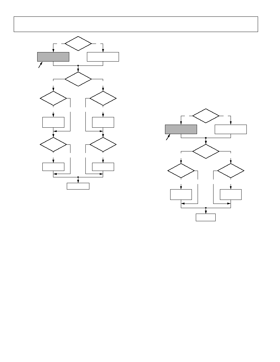
ADV7188
Rev. 0 | Page 48 of 112
05478-035
ADVANCE END OF
VSYNC BY PVEND[4:0]
DELAY END OF VSYNC
BY PVEND[4:0]
VSYNC END
PVENDSIGN
ODD FIELD?
0
1
NO
YES
PVENDDELO
VSEHO
ADDITIONAL
DELAY BY
1 LINE
ADVANCE BY
0.5 LINE
1
0
1
0
PVENDDELE
VSEHE
ADDITIONAL
DELAY BY
1 LINE
ADVANCE BY
0.5 LINE
1
0
1
0
NOT VALID FOR USER
PROGRAMMING
Figure 35. PAL VSYNC End
PVEND[4:0] PAL VSYNC End, Address 0xE9 [4:0]
The default value of PVEND is 10100, indicating the PAL
VSYNC end position.
For all NTSC/PAL VSYNC timing controls, both the V bit in
the AV code and the VSYNC on the VS pin are modified.
PFTOGDELO PAL Field Toggle Delay on Odd Field, Address
0xEA [7]
0 (default)--No delay.
1--Delays the F toggle/transition on an odd field by a line
relative to PFTOG.
PFTOGDELE PAL Field Toggle Delay on Even Field, Address
0xEA [6]
0 (default)--No delay.
1 (default)--Delays the F toggle/transition on an even field by a
line relative to PFTOG.
PFTOGSIGN PAL Field Toggle Sign, Address 0xEA [5]
0--Delays the field transition. Set for user manual
programming.
1 (default)--Advances the field transition. Not recommended
for user programming.
PFTOG PAL Field Toggle, Address 0xEA [4:0]
The default value of PFTOG is 00011, indicating the PAL field
toggle position.
For all NTSC/PAL field timing controls, the F bit in the AV
code and the field signal on the FIELD/DE pin are modified.
05478-036
ADVANCE TOGGLE OF
FIELD BY PTOG[4:0]
DELAY TOGGLE OF
FIELD BY PFTOG[4:0]
PFTOGSIGN
ODD FIELD?
0
1
NO
YES
PFTOGDELE
ADDITIONAL
DELAY BY
1 LINE
1
0
PFTOGDELO
ADDITIONAL
DELAY BY
1 LINE
1
0
FIELD
TOGGLE
NOT VALID FOR USER
PROGRAMMING
Figure 36. PAL F Toggle
SYNC PROCESSING
The ADV7188 has two additional sync processing blocks that
postprocess the raw synchronization information extracted
from the digitized input video. If desired, the blocks can be
disabled via the following two I
2
C bits.
ENHSPLL Enable HSYNC Processor, Address 0x01 [6]
The HSYNC processor is designed to filter incoming HSYNCs
that have been corrupted by noise, providing improved per-
formance for video signals with stable time bases but poor SNR.
0--Disables the HSYNC processor.
1 (default)--Enables the HSYNC processor.

ADV7188
Rev. 0 | Page 49 of 112
ENVSPROC Enable VSYNC Processor, Address 0x01 [3]
This block provides extra filtering of the detected VSYNCs to
give improved vertical lock.
0--Disables the VSYNC processor.
1 (default)--Enables the VSYNC processor.
VBI DATA DECODE
There are two VBI data slicers on the ADV7188. The first is
called is called the VBI data processor (VDP) and the second is
called VBI System 2.
The VDP can slice both low bandwidth standards and high
bandwidth standards such as Teletext. VBI System 2 can slice
low data-rate VBI standards only.
The VDP is capable of slicing multiple VBI data standards on
SD video. It decodes the VBI data on the incoming CVBS/YC
or YUV data. The decoded results are available as ancillary data
in output 656 data stream. For low data rate VBI standards like
CC/WSS/CGMS, the user can read the decoded data bytes from
I
2
C registers. The VBI data standards that can be decoded by
the VDP are
PAL
Teletext System A or C or D
ITU-BT-653
Teletext System B / WST
ITU-BT-653
VPS (Video Programming System)
ETSI EN 300 231 V 1.3.1
VITC (Vertical Interval Time Codes)
WSS (Wide Screen Signaling)
BT.1119-1/
ETSI.EN.300294
CCAP (Closed Captioning)
NTSC
Teletext System B and D
ITU-BT-653
Teletext System C/NABTS
ITU-BT-653 / EIA-516
VITC (Vertical Interval Time Codes)
CGMS (Copy Generation Management
System)
EIA-J CPR-1204 / IEC
61880
GEMSTAR
CCAP (Closed Captioning)
EIA-608
The VBI data standard that the VDP decodes on a particular
line of incoming video has been set by default as described in
Table 64. This can be overridden manually and any VBI data
can be decoded on any line. The details of manual program-
ming are described in Table 65 and Table 66.
VDP Default Configuration
The VDP can decode different VBI data standards on a line-to-
line basis. The various standards supported by default on
different lines of VBI are explained in Table 64.
VDP Manual Configuration
MAN_LINE_PGM Enable Manual Line Programming of VBI
Standards, Address 0x64 [7] User Sub Map
The user can configure the VDP to decode different standards on
a line-to-line basis through manual line programming. For this,
the user has to set the MAN_LINE_PGM bit. The user needs to
write into all the line programming registers VBI_DATA_Px_Ny
(Register 0x64 to Register 0x77, User Sub Map).
0 (default)--The VDP decodes default standards on lines as
shown in Table 64.
1--The VBI standards to be decoded are manually programmed.
VBI_DATA_Px_Ny [3:0] VBI Standard to be Decoded on
Line x for PAL, Line y for NTSC, Address 0x64-0x77, User
Sub Map
These are related 4-bit clusters contained from Register 0x64 to
Register 0x77 in the User Sub Map. The 4-bit, line
programming registers, named VBI_DATA_Px_Ny, identifies
the VBI data standard that would be decoded on line number X
in PAL or on line number Y in NTSC mode. The different types
of VBI standards decoded by VBI_DATA_Px_Ny are shown in
Table 65. Note that the interpretation of its value depends on
whether the ADV7188 is in PAL or NTSC mode.
ADV7188
Rev. 0 | Page 50 of 112
Table 64. Default Standards on Lines for PAL and NTSC
PAL 625/50
NTSC 525/60
Line No.
Default VBI
DATA Decoded
Line No.
Default VBI
DATA Decoded
Line No.
Default VBI
DATA Decoded
Line No.
Default VBI
DATA Decoded
6 WST
318
VPS
23
Gemstar-1x
7 WST
319 WST
24 Gemstar-1x
286 Gemstar-1x
8 WST
320 WST
25 Gemstar-1x
287 Gemstar-1x
9 WST
321 WST
288 Gemstar-1x
10 WST
322 WST
11 WST
323 WST
12 WST
324 WST
10 NABTS
272 NABTS
13 WST
325 WST
11 NABTS
273 NABTS
14 WST
326 WST
12 NABTS
274 NABTS
15 WST
327 WST
13 NABTS
275 NABTS
16 VPS
328 WST
14 VITC
276 NABTS
17
329 VPS
15 NABTS
277 VITC
18
330
16 VITC
278 NABTS
19 VITC
331
17 NABTS
279 VITC
20 WST
332 VITC
18 NABTS
280 NABTS
21 WST
333 WST
19 NABTS
281 NABTS
22 CCAP
334 WST
20 CGMS
282 NABTS
23
WSS 335
CCAP 21
CCAP 283
CGMS
24 + Full
ODD Field
WST
336
WST
22 + Full
ODD Field
NABTS 284
CCAP
337 + Full
EVEN Field
WST
285 + Full
EVEN Field
NABTS
Table 65. VBI Data Standards Manual Configuration
VBI_DATA_Px_Ny
625/50 PAL
525/60 NTSC
0000
Disable VDP
Disable VDP
0001
Teletext system identified by VDP_TTXT_TYPE
Teletext system identified by VDP_TTXT_TYPE
0010
VPS ETSI EN 300 231 V 1.3.1
Reserved
0011 VITC
VITC
0100
WSS BT.1119-1/ETSI.EN.300294
CGMS EIA-J CPR-1204/IEC 61880
0101 Reserved
Gemstar_1X
0110 Reserved
Gemstar_2X
0111 CCAP
CCAP
EIA-608
1000 1111
Reserved
Reserved
Table 66.VBI Data Standards to be Decoded on Line Px (PAL) or Line Ny (NTSC)
Address
Signal Name
Register Location
Dec Hex
VBI_DATA_P6_N23 VDP_LINE_00F[7:4]
101
0x65
VBI_DATA_P7_N24 VDP_LINE_010[7:4]
102
0x66
VBI_DATA_P8_N25 VDP_LINE_011[7:4]
103
0x67
VBI_DATA_P9 VDP_LINE_012[7:4]
104
0x68
VBI_DATA_P10 VDP_LINE_013[7:4]
105
0x69
VBI_DATA_P11 VDP_LINE_014[7:4]
106
0x6A
VBI_DATA_P12_N10 VDP_LINE_015[7:4]
107
0x6B
VBI_DATA_P13_N11 VDP_LINE_016[7:4]
108
0x6C
VBI_DATA_P14_N12 VDP_LINE_017[7:4]
109
0x6D
VBI_DATA_P15_N13 VDP_LINE_018[7:4]
110
0x6E
VBI_DATA_P16_N14 VDP_LINE_019[7:4]
111
0x6F
VBI_DATA_P17_N15 VDP_LINE_01A[7:4]
112
0x70
ADV7188
Rev. 0 | Page 51 of 112
Address
Signal Name
Register Location
Dec Hex
VBI_DATA_P18_N16 VDP_LINE_01B[7:4]
113
0x71
VBI_DATA_P19_N17 VDP_LINE_01C[7:4]
114
0x72
VBI_DATA_P20_N18 VDP_LINE_01D[7:4]
115
0x73
VBI_DATA_P21_N19 VDP_LINE_01E[7:4]
116
0x74
VBI_DATA_P22_N20 VDP_LINE_01F[7:4]
117
0x75
VBI_DATA_P23_N21 VDP_LINE_020[7:4]
118
0x76
VBI_DATA_P24_N22 VDP_LINE_021[7:4]
119
0x77
VBI_DATA_P318 VDP_LINE_00E[3:0]
100
0x64
VBI_DATA_P319_N286 VDP_LINE_00F[3:0]
101
0x65
VBI_DATA_P320_N287 VDP_LINE_010[3:0]
102
0x66
VBI_DATA_P321_N288 VDP_LINE_011[3:0]
103
0x67
VBI_DATA_P322 VDP_LINE_012[3:0]
104
0x68
VBI_DATA_P323 VDP_LINE_013[3:0]
105
0x69
VBI_DATA_P324_N272 VDP_LINE_014[3:0]
106
0x6A
VBI_DATA_P325_N273 VDP_LINE_015[3:0]
107
0x6B
VBI_DATA_P326_N274 VDP_LINE_016[3:0]
108
0x6C
VBI_DATA_P327_N275 VDP_LINE_017[3:0]
109
0x6D
VBI_DATA_P328_N276 VDP_LINE_018[3:0]
110
0x6E
VBI_DATA_P329_N277 VDP_LINE_019[3:0]
111
0x6F
VBI_DATA_P330_N278 VDP_LINE_01A[3:0]
112
0x70
VBI_DATA_P331_N279 VDP_LINE_01B[3:0]
113
0x71
VBI_DATA_P332_N280 VDP_LINE_01C[3:0]
114
0x72
VBI_DATA_P333_N281 VDP_LINE_01D[3:0]
115
0x73
VBI_DATA_P334_N282 VDP_LINE_01E[3:0]
116
0x74
VBI_DATA_P335_N283 VDP_LINE_01F[3:0]
117
0x75
VBI_DATA_P336_N284 VDP_LINE_020[3:0]
118
0x76
VBI_DATA_P337_N285 VDP_LINE_021[3:0]
119
0x77
Note:
Full field detection
(lines other than VBI lines) of any
standard can also be enabled by writing into registers
VBI_DATA_P24_N22[3:0] and VBI_DATA_P337_N285[3:0].
So, if VBI_DATA_P24_N22[3:0] is programmed with any
Teletext standard, then teletext is decoded off the whole of the
ODD field. The corresponding register for the EVEN field is
VBI_DATA_P337_N285[3:0].
Teletext System Identification:
VDP assumes that if teletext is
present in a video channel, all the teletext lines complies with a
single standard system. Thus, the line programming using
VBI_DATA_Px_Ny registers identifies whether the data in line
is teletext; the actual standard is identified by the
VDP_TTXT_TYPE_MAN bit. To program the
VDP_TTXT_TYPE_MAN bit, the
VDP_TTXT_TYPE_MAN_ENABLE bit must be set to 1.
VDP_TTXT_TYPE_MAN_ENABLE Enable Manual
Selection of Teletext Type, Address 0x60 [2], User Sub Map
0 (default)--Manual programming of the teletext type is
disabled.
1--Manual programming of the teletext type is enabled.
VDP_TTXT_TYPE_MAN [1:0] Specify the Teletext Type,
Address 0x60 [1:0], User Sub Map
These bits specify the teletext type to be decoded. These bits are
functional only if VDP_TTXT_TYPE_MAN_ENABLE is set to 1.
Table 67. VDP_TTXT_TYPE_MAN Function
VDP_TTXT_
TYPE_MAN [1:0]
Description
625/50 (PAL )
525/60 (NTSC).
00 (default)
Teletext-ITU-
BT.653- 625/50-A
Reserved
01
Teletext-ITU-
BT.653- 625/50-B
(WST)
Teletext-ITU-BT.653-
525/60-B
10
Teletext-ITU-
BT.653- 625/50-C
Teletext-ITU-BT.653-
525/60-C or EIA516
(NABTS)
11
Teletext-ITU-
BT.653- 625/50-.
Teletext-ITU-BT.653-
525/60-D

ADV7188
Rev. 0 | Page 52 of 112
VDP Ancillary Data Output
Reading the data back via I
2
C may not be feasible for VBI data
standards with high data rates (for example, teletext). An
alternative is to place the sliced data in a packet in the line
blanking of the digital output CCIR656 stream. This is available
for all standards sliced by the VDP module.
When data has been sliced on a given line, the corresponding
ancillary data packet is placed immediately after the next EAV
code that occurs at the output (that is, data sliced from multiple
lines are not buffered up and then emitted in a burst). Note that
the line number on which the packet is placed differs from the
line number on which the data was sliced due to the vertical
delay through the comb filters.
The user can enable or disable the insertion of VDP decoded
results into the 656 ancillary streams by using the
ADF_ENABLE bit.
ADF_ENABLE Enable Ancillary Data Output Through 656
Stream, Address 0x62 [7], User Sub Map
0 (default)--Disables insertion of VBI decoded data into
ancillary 656 stream.
1--Enables insertion of VBI decoded data into ancillary 656
stream.
The user may select the data identification word (DID) and the
secondary data identification word (SDID) through programming
the ADF_DID[4:0] and ADF_SDID[5:0] bits respectively as
explained below.
ADF_DID[4:0] User Specified Data ID Word in Ancillary
Data, Address 0x62 [4:0], User Sub Map
This bit selects the data ID word to be inserted in the ancillary
data stream with the data decoded by the VDP.
The default value of ADF_DID [4:0]is 10101.
ADF_SDID[5:0] User Specified Secondary Data ID Word in
Ancillary Data, Address 0x63 [5:0], User Sub Map
These bits select the secondary data ID word to be inserted in
the ancillary data stream with the data decoded by the VDP.
The default value of ADF_SDID [5:0]is 101010.
DUPLICATE_ADF Enable Duplication/Spreading of
Ancillary Data over Y and C Buses, Address 0x 63 [7], User
Sub Map
This bit determines whether the ancillary data is duplicated
over both Y and C buses or if the data packets are spread
between the two channels.
0 (default)--The ancillary data packet is spread across the Y and
C data streams.
1--The ancillary data packet is duplicated on the Y and C data
streams.
ADF_MODE [1:0] Determine the Ancillary Data Output
Mode, Address 0x62 [6:5], User Sub Map
These bits determine if the ancillary data output mode is in byte
mode or nibble mode.
ADF_MODE
[1:0] Description
00 (default)
Nibble mode.
01
Byte mode, no code restrictions.
10
Byte mode but 0x00 and 0xFF prevented (0x00
replaced by 0x01, 0xFF replaced by 0xFE)
11 Reserved.
The ancillary data packet sequence is explained in Table 68 and
Table 69. The nibble output mode is the default mode of output
from the ancillary stream when ancillary stream output is
enabled. This format is in compliance with ITU-R BT.1364.
Some definitions of the abbreviations used in Table 68 and
Table 69 are shown below:
·
EP.
Even parity for bits B8 to B2. This means that the parity
bit EP is set so that an even number of 1s are in bits in B8
to B2, including the parity bit, D8.
·
CS.
Checksum word. The CS word is used to increase
confidence of the integrity of the ancillary data packet
from the DID, SDID, and DC through user data-words
(UDWs). It consists of 10 bits: a 9-bit calculated value and
B9 as the inverse of B8. The checksum value B8 to B0 is
equal to the 9 LSBs of the sum of the 9 LSBs of the DID,
SDID, and DC and all UDWs in the packet. Prior to the
start of the checksum count cycle all checksum and carry
bits are pre-set to zero. Any carry resulting from the
checksum count cycle is ignored.
·
EP. The MSB B9 is the inverse EP. This ensures that
restricted codes 0x00 and 0xFF do not occur.
·
Line_number [9:0].
The line number of the line that
immediately precedes the ancillary data packet. The line
number is as per the numbering system in ITU-R BT.470.
The line number runs from 1 to 625 in a 625 line system
and from 1 to 263 in a 525 line system. Note the line
number on which the packet is output differs from the line
number on which the VBI data was sliced due to the
vertical delay through the comb filters.
·
Data Count.
The data count specifies the number of
UDWs in the ancillary stream for the standard. The total
number of user data-words = 4 × Data Count. Padding
words may be introduced to make the total number of
UDWs divisible by four.
ADV7188
Rev. 0 | Page 53 of 112
Table 68. Ancillary Data in Nibble Output Format
Byte B9
B8 B7
B6
B5
B4
B3 B2 B1
B0
Description
0 0
0
0 0
0
0
0 0
0
0
1 1
1
1 1
1
1
1 1
1
1
2 1
1
1 1
1
1
1 1
1
1
Ancillary data preamble
3
EP
EP 0
I2C_DID6_2[4:0]
0 0
DID (data identification
word)
4
EP
EP I2C_SDID7_2[5:0]
0
0
SDID (secondary data
identification word)
5
EP
EP 0
DC[4:0]
0 0 Data
count
6
EP
EP
padding[1:0]
VBI_DATA_STD[3:0]
0
0
ID0 (user data-word 1)
7
EP
EP
0
Line_number[9:5]
0
0
ID1 (user data-word 2)
8
EP
EP
Even_Field
Line_number[4:0]
0
0
ID2 (user data-word 3)
9
EP
EP
0
0
0
0
VDP_TTXT_TYPE[1:0]
0
0
ID3 (user data-word 4)
10
EP
EP
0
0
VBI_WORD_1[7:4]
0
0
User data-word 5
11
EP
EP
0
0
VBI_WORD_1[3:0]
0
0
User data-word 6
12
EP
EP
0
0
VBI_WORD_2[7:4]
0
0
User data-word 7
13
EP
EP
0
0
VBI_WORD_2[3:0]
0
0
User data-word 8
14
EP
EP
0
0
VBI_WORD_3[7:4]
0
0
User data-word 9
. .
.
. .
.
.
. .
.
.
. .
.
. .
.
.
. .
.
.
. .
.
. .
.
.
. .
.
.
n-3 1
0 0
0
0
0
0 0 0 0
n-2 1
0 0
0
0
0
0 0 0 0
[Pad 0x200, These
padding words may or
may not be present
depending on ancillary
data type] User data-
word XX
n-1
B8
Checksum
0
0
CS (checksum word)
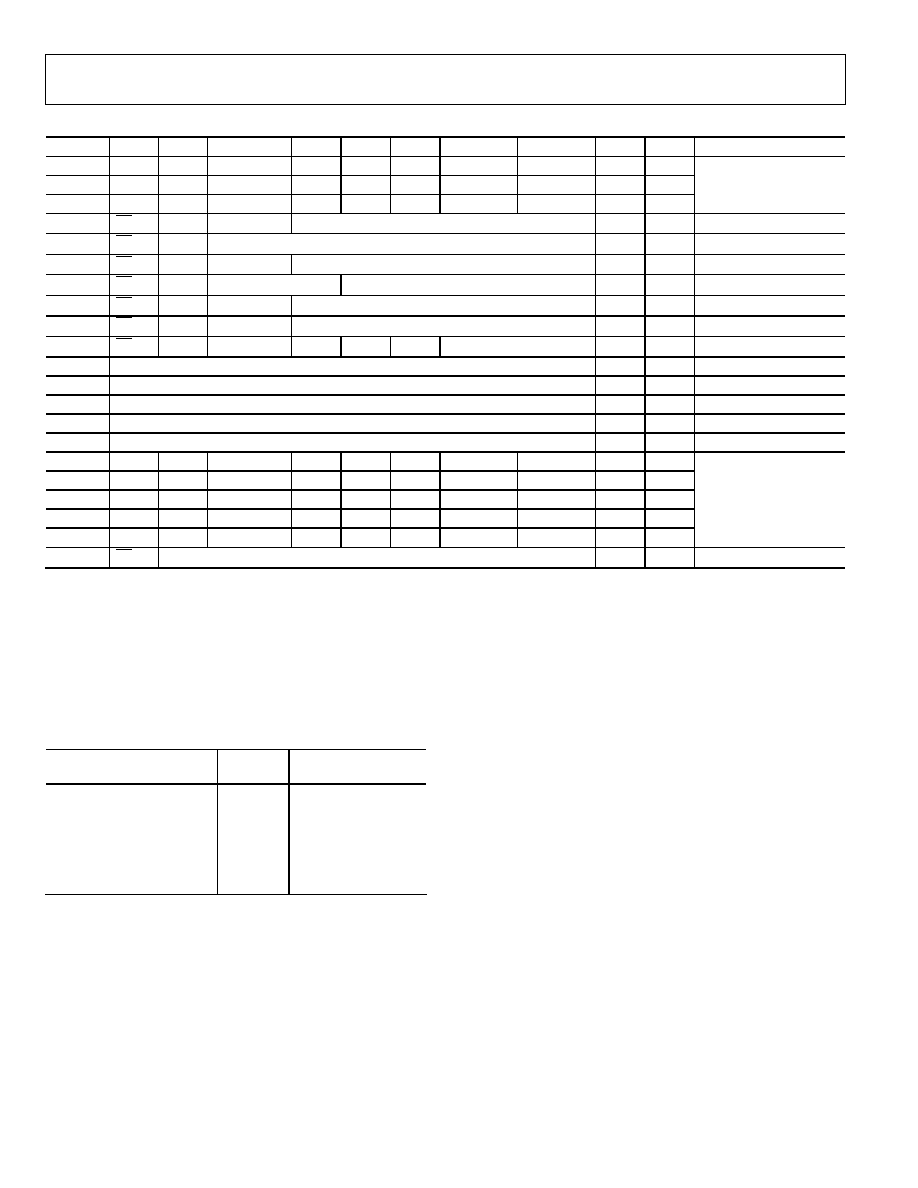
ADV7188
Rev. 0 | Page 54 of 112
Table 69. Ancillary Data in Byte Output Format
1
Byte B9 B8 B7
B6 B5 B4 B3
B2
B1 B0 Description
0
0 0 0
0 0 0 0
0
0 0
1
1 1 1
1 1 1 1
1
1 1
2
1 1 1
1 1 1 1
1
1 1
Ancillary data preamble
3
EP
EP
0
I2C_DID6_2[4:0]
0 0 DID
4
EP
EP
I2C_SDID7_2[5:0]
0 0 SDID
5
EP
EP
0
DC[4:0]
0 0 Data
count
6
EP
EP
padding[1:0]
VBI_DATA_STD[3:0]
0
0
ID0 (user data-word 1)
7
EP
EP
0
Line_number[9:5]
0
0
ID1 (user data-word 2)
8
EP
EP
Even_Field
Line_number[4:0]
0
0
ID2 (user data-word 3)
9
EP
EP
0
0 0 0 VDP_TTXT_TYPE[1:0] 0 0 ID3
(user
data-word
4)
10
VBI_WORD_1[7:0]
0 0 User
data-word
5
11
VBI_WORD_2[7:0]
0 0 User
data-word
6
12
VBI_WORD_3[7:0]
0 0 User
data-word
7
13
VBI_WORD_4[7:0]
0 0 User
data-word
8
14
VBI_WORD_5[7:0]
0 0 User
data-word
9
.
. . .
. . . .
.
. .
.
. . .
. . . .
.
. .
.
. . .
. . . .
.
. .
n-3 1 0 0
0 0 0 0
0
0 0
n-2 1 0 0
0 0 0 0
0
0 0
[Pad 0x200. These
padding words may or
may not be present
depending on ancillary
data type. User data-
word XX
n-1
B8
Checksum
0 0
1
This mode does not fully comply with ITU-R BT.1364.
Structure of VBI Words in Ancillary Data Stream
Each VBI data standard has been split into a clock-run-in
(CRI), a framing code (FC) and a number of data bytes (n). The
data packet in the ancillary stream includes only the FC and
data bytes. The VBI_WORD_X in the ancillary data stream has
the following format.
Table 70. Structure of VBI Data-Words in Ancillary Stream
Ancillary data byte
number
Byte
Type Byte
Description
VBI_WORD_1
FC0
Framing code [23:16].
VBI_WORD_2
FC1
Framing Code [15:8].
VBI_WORD_3
FC2
Framing Code [7:0].
VBI_WORD_4 DB1
1
st
data byte.
... ...
...
VBI_WORD_N+3
DBn
Last (nth) data byte.
VDP Framing Code
The length of the actual framing code depends on the VBI data
standard. For uniformity, the length of the framing code
reported in the ancillary data stream is always 24 bits. For
standards with a lesser framing code length, the extra LSB bits
are set to 0. The valid length of the framing code can be
decoded from the VBI_DATA_STD bit available in ID0
(UDW 1).
The framing code is always reported in the inverse-
transmission order. Table 71 shows the framing code and its
valid length for VBI data standards supported by VDP.
Example:
For teletext (B-WST) the framing code byte is 11100100
(0xE4),
bits shown in the order of transmission. Thus, VBI_WORD_1 =
0x27, VBI_WORD_2 = 0x00 and VBI_WORD_3 = 0x00.
Translating them into UDWs in the ancillary data stream, for
the nibble mode:
UDW5 [5:2] = 0010
UDW6 [5:2] = 0111
UDW7 [5:2] = 0000 (undefined bits made zeros)
UDW8 [5:2] = 0000 (undefined bits made zeros)
UDW9 [5:2] = 0000 (undefined bits made zeros)
UDW10 [5:2] = 0000 (undefined bits made zeros)
and for the byte mode:
UDW5 [9:2] = 0010_0111
UDW6 [9:2] = 0000_0000 (undefined bits made zeros)
UDW7 [9:2] = 0000_0000 (undefined bits made zeros)

ADV7188
Rev. 0 | Page 55 of 112
Data Bytes
The VBI_WORD_4 to VBI_WORD_N+3 contains the data-
words that were decoded by the VDP in the transmission order.
The position of bits in bytes is in the inverse transmission order.
For example, closed caption has two user data bytes as shown in
Table 76. The data bytes in the ancillary data stream would be as
follows:
VBI_WORD_4 = BYTE1 [7:0]
VBI_WORD_5 = BYTE2 [7:0]
The number of VBI_WORDS for each VBI data standard and
the total number of UDWs in the ancillary data stream is shown
in Table 72.
Table 71. Framing Code Sequence for Different VBI Standards
VBI Standard
Length in Bits
Error Free Framing Code bits
(In Order of Transmission )
Error Free Framing Code Reported by
VDP (In Reverse Order of Transmission )
TTXT_SYSTEM_A (PAL)
8
11100111
11100111
TTXT_SYSTEM_B (PAL)
8
11100100
00100111
TTXT_SYSTEM_B (NTSC)
8
11100100
00100111
TTXT_SYSTEM_C (PAL and NTSC)
8
11100111
11100111
TTXT_SYSTEM_D (PAL and NTSC)
8
11100101
10100111
VPS (PAL)
16
10001010100011001
1001100101010001
VITC (NTSC and PAL)
1
0
0
WSS (PAL)
24
000111100011110000011111
111110000011110001111000
GEMSTAR_1X (NTSC)
3
001
100
GEMSTAR_2X (NTSC)
11
1001_1011_101
101_1101_1001
CCAP (NTSC and PAL)
3
001
100
CGMS (NTSC)
1
0
0
Table 72. Total User Data Words for Different VBI Standards
1
VBI Standard
ADF Mode
Framing_code
UDWs
VBIData
Words
Number of
Padding Words
Total UDWs
00 (Nibble Mode)
6
74
0
84
TTXT_SYSTEM_A (PAL)
01,10 (Byte Mode)
3
37
0
44
00 (Nibble Mode)
6
84
2
96
TTXT_SYSTEM_B (PAL)
01,10 (Byte Mode)
3
42
3
52
00 (Nibble Mode)
6
68
2
80
TTXT_SYSTEM_B (NTSC)
01,10 (Byte Mode)
3
34
3
44
00 (Nibble Mode)
6
66
0
76
TTXT_SYSTEM_C (PAL and NTSC)
01,10 (Byte Mode)
3
33
2
42
00 (Nibble Mode)
6
68
2
80
TTXT_SYSTEM_D (PAL and NTSC)
01,10 (Byte Mode)
3
34
3
44
00 (Nibble Mode)
6
26
0
36
VPS (PAL)
01,10 (Byte Mode)
3
13
0
20
00 (Nibble Mode)
6
18
0
28
VITC (NTSC and PAL)
01,10 (Byte Mode)
3
9
0
16
00 (Nibble Mode)
6
4
2
16
WSS (PAL)
01,10 (Byte Mode)
3
2
3
12
00 (Nibble Mode)
6
4
2
16
GEMSTAR_1X (NTSC)
01,10 (Byte Mode)
3
2
3
12
00 (Nibble Mode)
6
8
2
20
GEMSTAR_2X (NTSC)
01,10 (Byte Mode)
3
4
1
12
00 (Nibble Mode)
6
4
2
16
CCAP (NTSC and PAL)
01,10 (Byte Mode)
3
2
3
12
00 (Nibble Mode)
6
6
0
16
CGMS (NTSC)
01,10 (Byte Mode)
3
3 + 3
2
12
1
The first four UDWs are always the ID.

ADV7188
Rev. 0 | Page 56 of 112
I
2
C Interface
Dedicated I
2
C readback registers are available for CCAP, CGMS,
WSS, Gemstar, VPS, PDC/UTC and VITC. Since Teletext is a high
data rate standard, data extraction is supported only through the
ancillary data packet. The details of these registers and their
access procedure are described below.
User Interface for I
2
C Readback Registers
The VDP decodes all enabled VBI data standards in real time.
Since the I
2
C access speed is much lower than the decoded rate,
when the registers are being accessed they may be updated with
data from the next line. In order to avoid this, VDP has a self-
clearing CLEAR bit and an AVAILABLE status bit accompanying
all the I
2
C readback registers.
The user has to clear the I
2
C readback register by writing a high
to the CLEAR bit. This resets the state of the AVAILABLE bit to
low and indicates that the data in the associated readback
registers is not valid. After the VDP decodes the next line of the
corresponding VBI data, the decoded data is placed in the I
2
C
readback register and the AVAILABLE bit is set to HIGH to
indicate that valid data is now available.
Though the VDP decodes this VBI data in subsequent lines if
present, the decoded data is not updated to the readback
registers until the CLEAR bit is set high again. However, this
data is available through the 656 ancillary data packets.
The CLEAR and AVAILABLE bits are in the VDP_CLEAR
(0x78, User Sub Map, write only) and VDP_STATUS (0x78,
User Sub Map, read only) registers.
Example I
2
C Readback Procedure
The following tasks have to be performed to read one packet
(line) of PDC data from the decoder.
·
Write 10 to I2C_GS_VPS_PDC_UTC[1:0] (0x9C, User Sub
Map) to specify that PDC data has to be updated to I2C
registers.
·
Write high to the GS_PDC_VPS_UTC_CLEAR bit (0x78,
User Sub Map) to enable I
2
C register updating.
·
Poll the GS_PDC_VPS_UTC_AVL bit (0x78, User Sub
Map) going high to check the availability of the PDC
packets.
·
Read the data bytes from the PDC I
2
C registers. To read
another line or packet of data the above steps have to be
repeated.
To read a packet of CC, CGMS, or WSS data, steps 1 through 3
only are required since they have dedicated registers.
VDP--Content-Based Data Update
For certain standards like WSS, CGMS, Gemstar, PDC, UTC,
and VPS the information content in the signal transmitted
remains the same over numerous lines and the user may want to
be notified only when there is a change in the information
content or loss of the information content. The user needs to
enable content-based updating for the required standard
through the GS_VPS_PDC_UTC_CB_CHANGE and
WSS_CGMS_CB_CHANGE bits. Thus the AVAILABLE bit
shows the availability of that standard only when its content has
changed.
Content-based updating also applies to loss of data at the lines
where some data was present before. Thus, for standards like
VPS, Gemstar, CGMS, and WSS, if no data arrives in the next
four lines programmed, then the corresponding AVAILABLE
bit in the VDP_STATUS register is set high and the content in
the I
2
C registers for that standard is set to zero. The user has to
write high to the corresponding CLEAR bit so that when a valid
line is decoded after some time, the decoded results are
available into the I
2
C registers, with the AVAILABLE status bit
set high.
If content-based updating is enabled, the AVAILABLE bit is set
high (assuming the CLEAR bit was written) in the following
cases:
·
The data contents change.
·
Data was being decoded and four lines with no data have
been detected.
·
No data was being decoded and new data is now being
decoded.
GS_VPS_PDC_UTC_CB_CHANGE Enable Content-Based
Updating for Gemstar/VPS/PDC/UTC, Address 0x9C [5],
User Sub Map
0--Disables content-based updating.
1 (default)--Enables content-based updating.
WSS_CGMS_CB_CHANGE Enable Content-Based Updating
for WSS/CGMS, Address 0x9C [4], User Sub Map
0--Disables content-based updating.
1 (default)--Enables content-based updating.
VDP--Interrupt-Based Reading of VDP I
2
C registers
Some VDP status bits are also linked to the interrupt request
controller so that the user does not have to poll the AVAILABLE
status bit. The user can configure the video decoder to trigger an
interrupt request on the INTRQ pin in response to the valid
data available in I
2
C registers. This function is available for the
following data types:

ADV7188
Rev. 0 | Page 57 of 112
CGMS or WSS:
The user can select between triggering an
interrupt request each time sliced data is available or triggering
an interrupt request only when the sliced data has changed.
Selection is made via the WSS_CGMS_CB_CHANGE bit.
Gemstar, PDC, VPS, or UTC
: The user can select between
triggering an interrupt request each time sliced data is available
or triggering an interrupt request only when the sliced data has
changed. Selection is made via the GS_VPS_PDC_UTC_
CB_CHANGE bit.
The sequence for the interrupt-based reading of the VDP I
2
C
data registers is the following for the CCAP standard.
1.
User unmasks CCAP interrupt mask bit (0x50 Bit 0, User
Sub Map = 1). CCAP data occurs on the incoming video.
VDP slices CCAP data and places it in the VDP readback
registers.
2.
The VDP CCAP available bit goes high and the VDP
module signals to the interrupt controller to stimulate an
interrupt request (for CCAP in this case).
3.
The user reads the interrupt status bits (User Sub Map) and
sees that new CCAP data is available (0x4E Bit 0, User Sub
Map = 1).
4.
The user writes 1 to the CCAP interrupt clear bit (0x4F Bit
0, User Sub Map = 1) in the Interrupt I
2
C space (this is a
self-clearing bit). This clears the interrupt on the INTRQ
pin but does NOT have an effect in the VDP I
2
C area.
5.
The user reads the CCAP data from the VDP I
2
C area.
6.
The user writes to a bit, CC_CLEAR in the VDP_STATUS
[0] register (0x78 Bit 0 User Sub Map = 1), to signify the
CCAP data has been read (=> the VDP CCAP can be
updated at the next occurrence of CCAP).
7.
Back to step 2.
Interrupt Mask Register Details
The following bits set the interrupt mask on the signal from the
VDP VBI data slicer.
VDP_CCAPD_MSKB Address 0x50 [0], User Sub Map
0 (default)--Disables interrupt on VDP_CCAPD_Q signal.
1--Enables interrupt on VDP_CCAPD_Q signal.
VDP_CGMS_WSS_CHNGD_MSKB Address 0x50 [2], User
Sub Map
0 (default)--Disables interrupt on
VDP_CGMS_WSS_CHNGD_Q signal.
1--Enables interrupt on VDP_CGMS_WSS_CHNGD_Q
signal.
VDP_GS_VPS_PDC_UTC_CHNG_MSKB Address 0x50 [4],
User Sub Map
0 (default)--Disables interrupt on
VDP_GS_VPS_PDC_UTC_CHNG_Q signal.
1--Enables interrupt on VDP_GS_VPS_PDC_UTC_CHNG_Q
signal.
VDP_VITC_MSKB Address 0x50 [6], User Sub Map
0 (default)--Disables interrupt on VDP_VITC_Q signal.
1--Enables interrupt on VDP_VITC_Q signal.
Interrupt Status Register Details
The following read-only bits contain data detection information
from the VDP module from the time the status bit has been last
cleared or unmasked.
VDP_CCAPD_Q Address 0x4E [0], User Sub Map
0 (default)--CCAP data has not been detected.
1--CCAP data has been detected.
VDP_CGMS_WSS_CHNGD_Q Address 0x4E [2], User Sub
Map
0 (default)--CGMS or WSS data has not been detected.
1--CGM or WSS data has been detected.
VDP_GS_VPS_PDC_UTC_CHNG_Q Address 0x4E [4], User
Sub Map
0 (default)--Gemstar, PDC, UTC, or VPS data has not been
detected.
1--Gemstar, PDC, UTC, or VPS data has been detected.
VDP_VITC_Q Address 0x4E [6], User Sub Map, read only
0 (default)--VITC data has not been detected.
1--VITC data has been detected.
Interrupt Status Clear Register Details
It is not necessary to write 0 to these write-only bits as they
automatically reset when they are set (self-clearing).
VDP_CCAPD_CLR Address 0x4F [0], User Sub Map
1--Clears VDP_CCAP_Q bit.
VDP_CGMS_WSS_CHNGD_CLR Address 0x4F [2], User
Sub Map
1--Clears VDP_CGMS_WSS_CHNGD_Q bit.
VDP_GS_VPS_PDC_UTC_CHNG_CLR Address 0x4F [4],
User Sub Map
1--Clears VDP_GS_VPS_PDC_UTC_CHNG_Q bit.
VDP_VITC_CLR Address 0x4F [6], User Sub Map
1--Clears VDP_VITC_Q bit.

ADV7188
Rev. 0 | Page 58 of 112
I
2
C READBACK REGISTERS
TELETEXT
Because teletext is a high data rate standard, the decoded bytes
are available only as ancillary data. However, a TTX_AVL bit
has been provided in I
2
C so that the user can check whether the
VDP has detected teletext. Note that the TTXT_AVL bit is a
plain status bit and does not use the protocol identified in the
I
2
C Interface section.
TTXT_AVL Teletext Detected Status bit, Address 0x78 [7],
User Sub Map, Read Only
0--Teletext was not detected.
1--Teletext was detected.
WST Packet Decoding
For WST ONLY, the VDP decodes the Magazine and Row
address of WST teletext packets and further decodes the
packet's 8x4 hamming coded words. This feature can be
disabled using WST_PKT_ DECOD_ DISABLE bit (Bit 3,
register 0x60, User Sub Map). The feature is valid for WST only.
WST_PKT_DECOD_DISABLE Disable Hamming Decoding
of Bytes in WST, Address 0x60 [3], User Sub Map
0--Enables hamming decoding of WST packets
1 (default)--Disables hamming decoding of WST packets.
For hamming coded bytes, the dehammed nibbles are output
along with some error information from the hamming decoder
as follows.
·
Input Hamming Coded byte: {D3, P3, D2, P2, D1, P1, D0,
P0} (bits in decoded order)
·
Output Dehammed byte: {E1, E0, 0, 0, D3', D2', D1', D0'}
(Di' corrected bits, Ei error info).
Table 73. Explanation of Error Bits in the Dehammed
Output Byte
E[1:0] Error
Information
Output Data Bits
in Nibble
00
No errors detected
OK
01
Error in P4
OK
10 Double
error
BAD
11
Single error found and corrected
OK
The different WST packets that are decoded are described in
Table 74.
Table 74. WST Packet Description
Packet Byte
Description
1P
st
Byte
Mag No. Dehammed Byte 4.
2P
nd
Byte
Row No. Dehammed Byte 5.
3
rd
Byte
Page No. Dehammed Byte 6.
4
th
Byte
Page No. Dehammed Byte 7.
5
th
to 10
th
Byte
Control Bytes Dehammed Byte 8 to Byte 13.
Header Packet
(X/00)
11
th
to 42
nd
Byte
Raw data bytes.
1
st
Byte
Mag No. Dehammed Byte 4.
2
nd
Byte
Row No. Dehammed Byte 5.
Text Packets
(X/01 to X/25)
3
rd
to 42
nd
Byte
Raw data bytes.
1
st
Byte
Mag No. Dehammed Byte 4.
2
nd
Byte
Row No. Dehammed Byte 5.
3
rd
Byte
Desig Code. Dehammed Byte 6.
4
th
Byte to 10
th
Byte
Dehammed Initial teletext Page Byte 7 to Byte 12.
11
th
to 23
rd
Byte
UTC bytes Dehammed Bytes 13 to Byte 25.
8/30 (Format 1) packet
Desig Code = 0000 or 0001
UTC
24
th
to 42
nd
Byte
Raw status bytes.
1
st
Byte
Mag No. Dehammed Byte 4.
2
nd
Byte
Row No. Dehammed Byte 5.
3
rd
Byte
Desig Code. Dehammed Byte 6.
4
th
Byte to 10
th
Byte
Dehammed Initial teletext Page Byte 7 to Byte 12.
11
th
to 23
rd
Byte
PDC bytes Dehammed Byte 13 to Byte 25.
8/30 (Format 2) packet
Desig Code = 0010 or 0011
PDC
24
th
to 42
nd
Byte
Raw status bytes.
1
st
Byte
Mag No. Dehammed Byte 4.
2
nd
Byte
Row No. Dehammed Byte 5.
3
rd
Byte
Desig Code. Dehammed Byte 6.
X/26, X/27, X/28, X/29, X/30, X/31
1
4
th
to 42
nd
Byte
Raw data bytes.
1
For X/26, X/28 and M/29, further decoding needs 24x18 hamming decoding. Not supported at present.
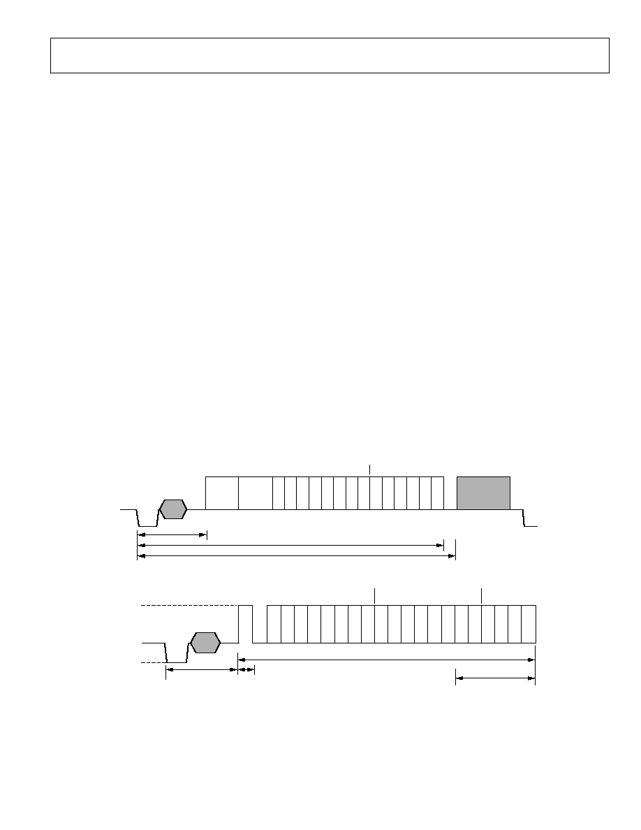
ADV7188
Rev. 0 | Page 59 of 112
CGMS and WSS
The CGMS and WSS data packets convey the same type of
information for different video standards. WSS is for PAL and
CGMS is for NTSC and hence the CGMS and WSS readback
registers are shared. WSS is bi-phase coded; the VDP does a bi-
phase decoding to produce the 14 raw WSS bits in the
CGMS/WSS readback I
2
C registers and sets the
CGMS_WSS_AVL bit.
CGMS_WSS_CLEAR, CGMS/WSS Clear, Address 0x78 [2],
User Sub Map, Write Only, Self -Clearing
1--Re-initializes the CGMS/WSS readback registers.
CGMS_WSS_AVL CGMS/WSS Available Bit, Address 0x78
[2], User Sub Map, Read Only
0--CGMS/WSS was not detected.
1--CGMS/WSS was detected.
CGMS_WSS_DATA_0[3:0], Address 0x7D [3:0]
CGMS_WSS_DATA_1[7:0], Address 0x7E [7:0]
CGMS_WSS_DATA_2[7:0], Address 0x7F [7:0]
User Sub Map, read only. These bits hold the decoded CGMS or
WSS data.
Refer to Figure 37 and Figure 38 for the I
2
C to WSS and CGMS
bit mapping.
CCAP
Two bytes of decoded closed caption data are available in the
I
2
C registers. The field information of the decoded CCAP data
can be obtained from the CC_EVEN_FIELD bit (register 0x78).
CC_CLEAR Closed Caption Clear, Address 0x78 [0] User
Sub Map, Write Only, Self-Clearing
1--Re-initializes the CCAP readback registers.
CC_AVL Closed Caption Available, Address 0x78 [0], User
Sub Map, Read Only
0--Closed captioning was not detected.
1--Closed captioning was detected.
CC_EVEN_FIELD Address 0x78 [1], User Sub Map, Read
Only
Identifies the field from which the CCAP data was decoded.
0--Closed captioning detected on an ODD field.
1--Closed captioning was detected on an EVEN field.
VDP_CCAP_DATA_0 Address 0x79 [7:0], User Sub Map,
Read Only
Decoded Byte 1 of CCAP data.
VDP_CCAP_DATA_1 Address 0x7A [7:0], User Sub Map,
Read Only
Decoded Byte 2 of CCAP data.
05478-037
ACTIVE
VIDEO
VDP_CGMS_WSS_
DATA_1[5:0]
VDP_CGMS_WSS_DATA_2
RUN-IN
SEQUENCE
START
CODE
0
1
2
3
4
5
6
7
0
1
2
3
4
5
11.0
s
38.4
s
42.5
s
Figure 37. WSS Waveform
05478-038
0
1
2
3
4
5
6
7
0
1
2
3
4
5
6
7
0
1
2
3
VDP_CGMS_WSS_DATA_1
VDP_CGMS_WSS_
DATA_0[3:0]
VDP_CGMS_WSS_DATA_2
REF
+100 IRE
+70 IRE
0 IRE
40 IRE
11.2
s
49.1
s
±
0.5
s
CRC SEQUENCE
2.235
s
±
20ns
Figure 38. CGMS Waveform
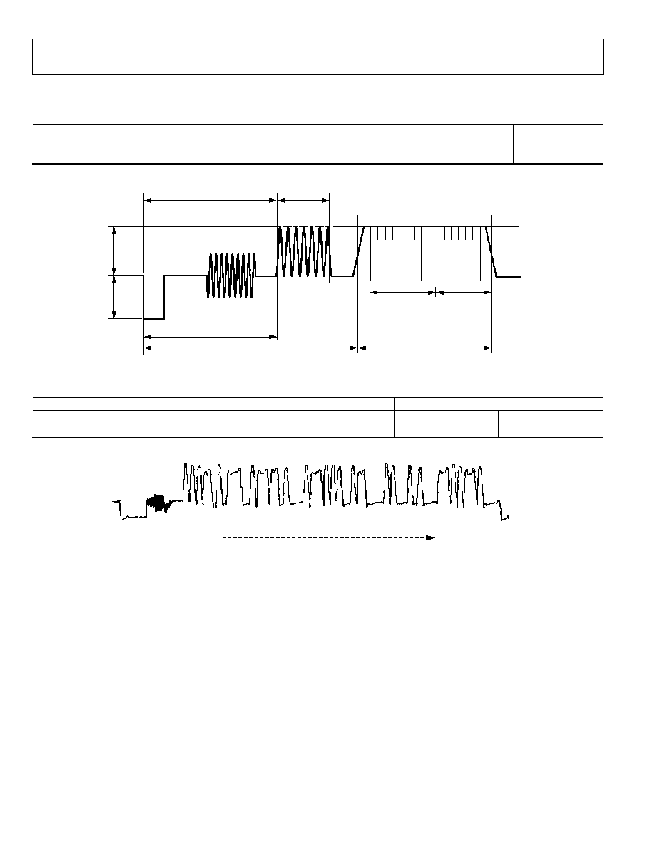
ADV7188
Rev. 0 | Page 60 of 112
Table 75. CGMS Readback Registers
1
Signal Name
Register Location
Address (User Sub Map)
CGMS_WSS_DATA_0[3:0] VDP_CGMS_WSS_DATA_0
[3:0] 125d
0x7D
CGMS_WSS_DATA_1[7:0] VDP_CGMS_WSS_DATA_1
[7:0] 126d
0x7E
CGMS_WSS_DATA_2[7:0] VDP_CGMS_WSS_DATA_2
[7:0] 127d
0x7F
1
The register is a readback register; default value does not apply.
0
REFERENCE COLOR BURST
(9 CYCLES)
FREQUENCY = F
SC
= 3.579545MHz
AMPLITUDE = 40 IRE
1
7 CYCLES
OF 0.5035MHz
(CLOCK RUN-IN)
2 3 4 5 6 7 0 1 2 3 4 5 6 7
P
A
R
I
T
Y
S
T
A
R
T
P
A
R
I
T
Y
VDP_CCAP_DATA_0
33.764
s
10.003
s
10.5
±
0.25
s
12.91
s
27.382
s
50 IRE
40 IRE
05478-039
VDP_CCAP_DATA_1
Figure 39.CCAP Waveform and Decoded Data Correlation
Table 76: CCAP Readback Registers
1
Signal Name
Register Location
Address (User Sub Map)
CCAP_BYTE_1[7:0] VDP_CCAP_DATA_0[7:0] 121d
0x79
CCAP_BYTE_2[7:0] VDP_CCAP_DATA_1[7:0] 122d
0x7A
1
The register is a readback register; default value does not apply.
BIT0, BIT1
BIT88, BIT89
TO
VITC WAVEFORM
05478-040
Figure 40. VITC Waveform and Decoded Data Correlation
VITC
VITC has a sync sequence of 10 in between each data byte. The
VDP strips these syncs from the data stream to give out only the
data bytes. The VITC results are available in VDP_VITC_DATA_0
to VDP_VITC_DATA_8 registers (Register 0x92 to Register
0x9A, User Sub Map).
The VITC has a CRC byte at the end; the in-between syncs are
also used in this CRC calculation. Since the in-between syncs
are not given out, the CRC is also calculated internally. The
calculated CRC is also available for the user in VITC_CALC_CRC
register (Resister 0x9B, User Sub Map). Once the VDP completes
decoding the VITC line, the VITC_DATA and VITC_CALC_CRC
registers are updated and VITC_AVL bit is set.
VITC_CLEAR VITC Clear, Address 0x78 [6], User Sub Map,
Write Only, Self-Clearing
1--Re-initializes the VITC readback registers.
VITC_AVL VITC Available, Address 0x78 [6], User Sub Map
0--VITC data was not detected.
1--VITC data was detected.
VITC Readback Registers
See Figure 40 for the I
2
C to VITC bit mapping.

ADV7188
Rev. 0 | Page 61 of 112
Table 77. VITC Readback Registers
1
Signal Name
Register Location
Address (User Sub Map)
VITC_DATA_0[7:0] VDP_VITC_DATA_0[7:0]
(VITC bits [9:2]
146
0x92
VITC_DATA_1[7:0] VDP_VITC_DATA_1[7:0]
(VITC bits [19:12]
147
0x93
VITC_DATA_2[7:0] VDP_VITC_DATA_2[7:0]
(VITC bits [29:22]
148
0x94
VITC_DATA_3[7:0] VDP_VITC_DATA_3[7:0]
(VITC bits [39:32]
149
0x95
VITC_DATA_4[7:0] VDP_VITC_DATA_4[7:0]
(VITC bits [49:42]
150
0x96
VITC_DATA_5[7:0] VDP_VITC_DATA_5[7:0]
(VITC bits [59:52]
151
0x97
VITC_DATA_6[7:0] VDP_VITC_DATA_6[7:0]
(VITC bits [69:62]
152
0x98
VITC_DATA_7[7:0] VDP_VITC_DATA_7[7:0]
(VITC bits [79:72]
153
0x99
VITC_DATA_8[7:0] VDP_VITC_DATA_8[7:0]
(VITC bits [89:82]
154
0x9A
VITC_CALC_CRC[7:0] VDP_VITC_CALC_CRC[7:0]
155 0x9B
1
The register is a readback register; default value does not apply.
VPS/PDC/UTC/GEMSTAR
The readback registers for VPS, PDC and UTC have been
shared. Gemstar is a high data rate standard and so is available
only through the ancillary stream; however, for evaluation
purposes, any one line of Gemstar is available through I
2
C
registers sharing the same register space as PDC, UTC and VPS.
Thus only one standard out of VPS, PDC, UTC and Gemstar
can be read through the I
2
C at a time.
To identify the data that should be made available in the I
2
C
registers, the user has to program I2C_GS_VPS_PDC_UTC[1:0]
(register address 0x9C, User Sub Map).
I2C_GS_VPS_PDC_UTC (VDP) [1:0] Address 0x9C [6:5],
User Sub Map
Specifies which standard result to be available for I
2
C readback.
Table 78. I2C_GS_VPS_PDC_UTC[1:0] Function
I2C_GS_VPS_PDC_UTC
[1:0]
Description
00 (default)
Gemstar 1x/2x.
01 VPS.
10 PDC.
11 UTC.
GS_PDC_VPS_UTC_CLEAR GS/PDC/VPS/UTC Clear,
Address 0x78 [4], User Sub Map, Write Only, Self-Clearing
1--Re-initializes the GS/PDC/VPS/UTC data readback
registers.
GS_PDC_VPS_UTC_AVL GS/PDC/VPS/UTC Available,
Address 0x78 [4], User Sub Map, Read Only
0--One of GS, PDC, VPS or UTC data was not detected.
1--One of GS, PDC, VPS, or UTC data was detected.
VDP_GS_VPS_PDC_UTC Readback Registers
See Table 79.
VPS
The VPS data bits are bi-phase decoded by the VDP. The
decoded data is available in both the ancillary stream and in the
I
2
C readback registers. VPS decoded data is available in the
VDP_GS_VPS_PDC_UTC_0 to VDP_VPS_PDC_UTC_12
registers (addresses 0x84 0x90, User Sub Map). The GS_VPS_
PDC_UTC_AVL bit is set if the user had programmed
I2C_GS_VPS_PDC_UTC to 01, as explained in Table 78.
GEMSTAR
The Gemstar decoded data is made available in the ancillary
stream and any one line of Gemstar is also available in I
2
C
registers for evaluation purposes. To obtain Gemstar results in
I
2
C registers, the user has to program I2C_GS_VPS_
PDC_UTC to 00, as explained in Table 78.
VDP supports auto detection of Gemstar standard between
Gemstar 1× or Gemstar 2× and decodes accordingly. For this
auto detection mode to work the user has to set
AUTO_DETECT_GS_TYPE I
2
C bit (register 0x61 User Sub
Map) and program the decoder to decode Gemstar 2× on the
required lines through line programming. The type of Gemstar
decoded can be determined by observing the bit
GS_DATA_TYPE bit (Register 0x78, User Sub Map).
AUTO_DETECT_GS_TYPE, Address 0x61 [4], User Sub Map
0 (default)--Disables autodetection of Gemstar type.
1--Enables autodetection.
GS_DATA_TYPE, Address 0x78 [5], User Sub Map, Read Only
Identifies the decoded Gemstar data type.
0--Gemstar 1× mode is detected. Read 2 data bytes from 0x84.
1--Gemstar 2× mode is detected. Read 4 data bytes from 0x84.
The Gemstar data that is available in the I
2
C register could be
from any line of the input video on which Gemstar was
decoded. To read the Gemstar data on a particular video line,
the user should use the Manual Configuration as described in
Table 65 and Table 66 and enable Gemstar decoding on the
required line only.

ADV7188
Rev. 0 | Page 62 of 112
Table 79. GS /VPS/PDC/UTC Readback Registers
1
Address (User Sub Map)
Signal Name
Register Location
Dec
Hex
GS_VPS_PDC_UTC_BYTE_0[7:0] VDP_GS_VPS_PDC_UTC_0[7:0] 132d
0x84
GS_VPS_PDC_UTC_BYTE_1[7:0] VDP_GS_VPS_PDC_UTC_1[7::0] 133d
0x85
GS_VPS_PDC_UTC_BYTE_2[7:0] VDP_GS_VPS_PDC_UTC_2[7:0] 134d
0x86
GS_VPS_PDC_UTC_BYTE_3[7:0] VDP_GS_VPS_PDC_UTC_3[7:0] 135d
0x87
VPS_PDC_UTC_BYTE_4[7:0] VDP_VPS_PDC_UTC_4[7:0] 136d
0x88
VPS_PDC_UTC_BYTE_5[7:0] VDP_VPS_PDC_UTC_5[7:0] 137d
0x89
VPS_PDC_UTC_BYTE_6[7:0] VDP_VPS_PDC_UTC_6[7:0] 138d
0x8A
VPS_PDC_UTC_BYTE_7[7:0] VDP_VPS_PDC_UTC_7[7:0] 139d
0x8B
VPS_PDC_UTC_BYTE_8[7:0] VDP_VPS_PDC_UTC_8[7:0] 140d
0x8C
VPS_PDC_UTC_BYTE_9[7:0] VDP_VPS_PDC_UTC_9[7:0] 141d
0x8D
VPS_PDC_UTC_BYTE_10[7:0] VDP_VPS_PDC_UTC_10[7:0] 142d
0x8E
VPS_PDC_UTC_BYTE_11[7:0] VDP_VPS_PDC_UTC_11[7:0] 143d
0x8F
VPS_PDC_UTC_BYTE_12[7:0] VDP_VPS_PDC_UTC_12[7:0] 144d
0x90
1
The register is a readback register; default value does not apply.
PDC/UTC
PDC and UTC are data transmitted through teletext packet
8/30 format 2 (magazine 8, row 30, design_code 2 or 3), and
packet 8/30 format 1 (magazine 8, row 30, design_code 0 or 1).
Hence, if PDC or UTC data is to be read through I
2
C, the
corresponding teletext standard (WST or PAL System B) should
be decoded by VDP. The whole teletext decoded packet is
output on the ancillary data stream. The user can look for the
magazine number, row number and design_code and qualify
the data as PDC, UTC or none of these.
If PDC/UTC packets have been identified, Byte 0 to Byte 12 are
updated to the GS_VPS_PDC_UTC_0 to VPS_PDC_UTC_12
registers, and the GS_VPS_PDC_UTC_AVL bit set. The full
packet data is also available in the ancillary data format.
Note that the data available in the I
2
C register depends on the
status of the WST_PKT_DECODE_DISABLE bit (Bit 3,
subaddress 0x60, User Sub Map).
VBI SYSTEM 2
The user has an option of using a different VBI data slicer called
VBI System 2. This data slicer is used to decode Gemstar and
Closed Caption VBI signals only.
Using this system, the Gemstar data is only available in the
ancillary data stream. A special mode enables one line of data to
be read back via I
2
C. For details on how to get I
2
C readback
when using the VBI System 2 data slicer, see the ADI
applications note on ADV7188 VBI processing.
Gemstar Data Recovery
The Gemstar-compatible data recovery block (GSCD) supports
1× and 2× data transmissions. In addition, it can serve as a
closed caption decoder. Gemstar-compatible data transmissions
can occur only in NTSC. Closed caption data can be decoded in
both PAL and NTSC.
The block is configured via I
2
C in the following ways:
·
GDECEL[15:0] allows data recovery on selected video lines
on even fields to be enabled and disabled.
·
GDECOL[15:0] enables the data recovery on selected lines
for odd fields.
·
GDECAD configures the way in which data is embedded
in the video data stream.
The recovered data is not available through I
2
C, but is inserted
into the horizontal blanking period of an ITU-R. BT656-
compatible data stream. The data format is intended to comply
with the recommendation by the International
Telecommunications Union, ITU-R BT.1364. For more
information, see the ITU website at www.itu.ch. See Figure 41.
GDE_SEL_OLD_ADF, Address 0x4C [3], User Map
The ADV7188 has a new ancillary data output block that can be
used by the VDP data slicer and the VBI System 2 data slicer.
The new ancillary data formatter is used by setting
GDE_SEL_OLD_ADF = 0 (this is the default setting). If this bit
is set low, refer to Table 68 and Table 69 for information about
how the data is packaged in the ancillary data stream.
To use the old ancillary data formatter (to be backward
compatible with the ADV7189B), set GDE_SEL_OLD_ADF = 1.
The ancillary data format in this section refers to the
ADV7189B-compatible ancillary data formatter.
0(default)--Enables new ancillary data system (for use with
VDP and VBI System 2)
1--Enables old ancillary data system (for use with VBI System 2
only; ADV7189B-compatible).
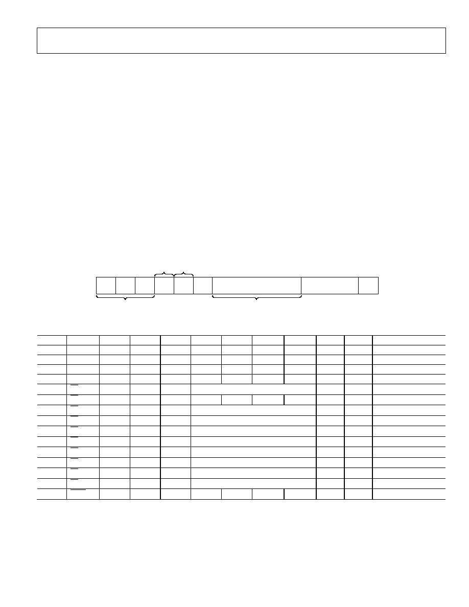
ADV7188
Rev. 0 | Page 63 of 112
The format of the data packet depends on the following criteria:
·
Transmission is 1× or 2×.
·
Data is output in 8-bit or 4-bit format (see the description
of the GDECAD Gemstar Decode Ancillary Data Format,
Address 0x4C [0] bit).
·
Data is closed caption (CCAP) or Gemstar-compatible.
Data packets are output if the corresponding enable bit is set
(see the GDECEL[15:0] and GDECOL[15:0] descriptions), and
if the decoder detects the presence of data. This means that for
video lines where no data has been decoded, no data packet is
output even if the corresponding line enable bit is set.
Each data packet starts immediately after the EAV code of the
preceding line. Figure 41 and Table 80 show the overall
structure of the data packet.
Entries within the packet are as follows:
·
Fixed preamble sequence of 0x00, 0xFF, 0xFF.
·
Data identification word (DID). The value for the DID
marking a Gemstar or CCAP data packet is 0x140 (10-bit
value).
·
Secondary data identification word (SDID), which contains
information about the video line from which data was
retrieved, whether the Gemstar transmission was of 1× or
2× format, and whether it was retrieved from an even or
odd field.
·
Data count byte, giving the number of user data-words that
follow.
·
User data section.
·
Optional padding to ensure that the length of the user
data-word section of a packet is a multiple of four bytes
(requirement as set in ITU-R BT.1364).
·
Checksum byte.
Table 80 lists the values within a generic data packet that is
output by the ADV7188 in 10-bit format.
05478-045
00
FF
FF
DID
SDID
DATA
COUNT
USER DATA
OPTIONAL PADDING
BYTES
CHECK
SUM
SECONDARY DATA IDENTIFICATION
PREAMBLE FOR ANCILLARY DATA
DATA IDENTIFICATION
USER DATA (4 OR 8 WORDS)
Figure 41. Gemstar and CCAP Embedded Data Packet (Generic)
Table 80. Generic Data Output Packet
Byte D[9] D[8] D[7] D[6] D[5] D[4] D[3] D[2] D[1] D[0] Description
0 0 0 0 0 0 0 0 0 0 0 Fixed
preamble
1 1 1 1 1 1 1 1 1 1 1 Fixed
preamble
2 1 1 1 1 1 1 1 1 1 1 Fixed
preamble
3 0 1 0 1 0 0 0 0 0 0 DID
4
EP
EP EF 2X
line[3:0]
0 0 SDID
5
EP
EP
0 0 0 0 DC[1]
DC[0]
0 0 Data
count
(DC)
6
EP
EP 0 0
word1[7:4]
0 0 User data-words
7
EP
EP 0 0
word1[3:0]
0 0 User
data-words
8
EP
EP 0 0
word2[7:4]
0 0 User
data-words
9
EP
EP 0 0
word2[3:0]
0 0 User
data-words
10
EP
EP 0 0
word3[7:4]
0 0 User
data-words
11
EP
EP 0 0
word3[3:0]
0 0 User
data-words
12
EP
EP 0 0
word4[7:4]
0 0 User
data-words
13
EP
EP 0 0
word4[3:0]
0 0 User
data-words
14
CS[8]
CS[8] CS[7] CS[6] CS[5] CS[4] CS[3] CS[2] 0
0
Checksum

ADV7188
Rev. 0 | Page 64 of 112
Table 81. Data Byte Allocation
2×
Raw Information Bytes
Retrieved from the Video Line
GDECAD
User Data-Words
(Including Padding)
Padding Bytes
DC[1:0]
1 4
0
8
0
10
1 4
1
4
0
01
0 2
0
4
0
01
0 2
1
4
2
01
Gemstar Bit Names
·
DID. The data identification value is 0x140 (10-bit value).
Care has been taken that in 8-bit systems, the two LSBs do
not carry vital information.
·
EP and EP. The EP bit is set to ensure even parity on the
data-word D[8:0]. Even parity means there is always an
even number of 1s within the D[8:0] bit arrangement. This
includes the EP bit. EP describes the logic inverse of EP
and is output on D[9]. The EP is output to ensure that the
reserved codes of 00 and FF cannot happen.
·
EF. Even field identifier. EF = 1 indicates that the data was
recovered from a video line on an even field.
·
2×. This bit indicates whether the data sliced was in
Gemstar 1× or 2× format. A high indicates 2× format.
·
line[3:0]. This entry provides a code that is unique for each
of the possible 16 source lines of video from which
Gemstar data may have been retrieved. Refer to Table 90
and Table 91.
·
DC[1:0]. Data count value. The number of UDWs in the
packet divided by 4. The number of UDWs in any packet
must be an integral number of 4. Padding is required at the
end, if necessary, as set in ITU-R BT.1364. See Table 81.
·
The 2× bit determines whether the raw information
retrieved from the video line was 2 or 4 bytes. The state of
the GDECAD bit affects whether the bytes are transmitted
straight (that is, two bytes transmitted as two bytes) or
whether they are split into nibbles (that is, two bytes
transmitted as four half bytes). Padding bytes are then
added where necessary.
·
CS[8:2]. The checksum is provided to determine the
integrity of the ancillary data packet. It is calculated by
summing up D[8:2] of DID, SDID, the data count byte, and
all UDWs, and ignoring any overflow during the
summation. Since all data bytes that are used to calculate
the checksum have their 2 LSBs set to 0, the CS[1:0] bits
are also always 0.
CS[8] describes the logic inversion of CS[8]. The value
CS[8] is included in the checksum entry of the data packet
to ensure that the reserved values of 0x00 and 0xFF do not
occur. Table 82 to Table 87 outline the possible data
packages.
Gemstar 2× Format, Half-Byte Output Mode
Half-byte output mode is selected by setting CDECAD = 0;
full-byte output mode is selected by setting CDECAD = 1. See
the GDECAD Gemstar Decode Ancillary Data Format,
Address 0x4C [0] section.
Gemstar 1× Format
Half-byte output mode is selected by setting CDECAD = 0,
full-byte output mode is selected by setting CDECAD = 1. See
the GDECAD Gemstar Decode Ancillary Data Format,
Address 0x4C [0] section.
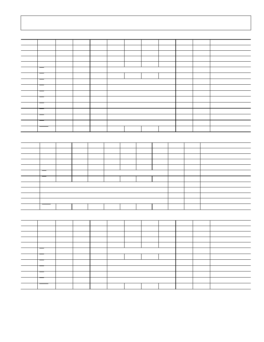
ADV7188
Rev. 0 | Page 65 of 112
Table 82. Gemstar 2× Data, Half-Byte Mode
Byte D[9] D[8] D[7] D[6] D[5] D[4] D[3] D[2] D[1] D[0] Description
0 0 0 0 0 0 0 0 0 0 0 Fixed
preamble
1 1 1 1 1 1 1 1 1 1 1 Fixed
preamble
2 1 1 1 1 1 1 1 1 1 1 Fixed
preamble
3 0 1 0 1 0 0 0 0 0 0 DID
4
EP
EP EF 1
line[3:0]
0 0 SDID
5
EP
EP
0 0 0 0 1 0 0 0 Data
count
6
EP
EP 0 0
Gemstar word1[7:4]
0 0 User data-words
7
EP
EP 0 0
Gemstar word1[3:0]
0 0 User
data-words
8
EP
EP 0 0
Gemstar word2[7:4]
0 0 User
data-words
9
EP
EP 0 0
Gemstar word2[3:0]
0 0 User
data-words
10
EP
EP 0 0
Gemstar word3[7:4]
0 0 User
data-words
11
EP
EP 0 0
Gemstar word3[3:0]
0 0 User
data-words
12
EP
EP 0 0
Gemstar word4[7:4]
0 0 User
data-words
13
EP
EP 0 0
Gemstar word4[3:0]
0 0 User
data-words
14
CS[8]
CS[8] CS[7] CS[6] CS[5] CS[4] CS[3] CS[2] CS[1] CS[0] Checksum
Table 83. Gemstar 2× Data, Full-Byte Mode
Byte D[9] D[8] D[7] D[6] D[5] D[4] D[3] D[2] D[1] D[0] Description
0 0 0 0 0 0 0 0 0 0 0 Fixed
preamble
1 1 1 1 1 1 1 1 1 1 1 Fixed
preamble
2 1 1 1 1 1 1 1 1 1 1 Fixed
preamble
3 0 1 0 1 0 0 0 0 0 0 DID
4
EP
EP EF 1
line[3:0]
0 0 SDID
5
EP
EP
0 0 0 0 0 1 0 0 Data
count
6
Gemstar
word1[7:0]
0 0 User
data-words
7
Gemstar
word2[7:0]
0 0 User
data-words
8
Gemstar
word3[7:0]
0 0 User
data-words
9
Gemstar
word4[7:0]
0 0 User
data-words
10
CS[8]
CS[8] CS[7] CS[6] CS[5] CS[4] CS[3] CS[2] CS[1] CS[0] Checksum
Table 84. Gemstar 1× Data, Half-Byte Mode
Byte D[9] D[8] D[7] D[6] D[5] D[4] D[3] D[2] D[1] D[0] Description
0 0 0 0 0 0 0 0 0 0 0 Fixed
preamble
1 1 1 1 1 1 1 1 1 1 1 Fixed
preamble
2 1 1 1 1 1 1 1 1 1 1 Fixed
preamble
3 0 1 0 1 0 0 0 0 0 0 DID
4
EP
EP EF 0
line[3:0]
0 0 SDID
5
EP
EP
0 0 0 0 0 1 0 0 Data
count
6
EP
EP 0 0
Gemstar word1[7:4]
0 0 User data-words
7
EP
EP 0 0
Gemstar word1[3:0]
0 0 User
data-words
8
EP
EP 0 0
Gemstar word2[7:4]
0 0 User
data-words
9
EP
EP 0 0
Gemstar word2[3:0]
0 0 User
data-words
10
CS[8]
CS[8] CS[7] CS[6] CS[5] CS[4] CS[3] CS[2] CS[1] CS[0] Checksum
ADV7188
Rev. 0 | Page 66 of 112
Table 85. Gemstar 1× Data, Full-Byte Mode
Byte D[9] D[8] D[7] D[6] D[5] D[4] D[3] D[2] D[1] D[0] Description
0 0 0 0 0 0 0 0 0 0 0 Fixed
preamble
1 1 1 1 1 1 1 1 1 1 1 Fixed
preamble
2 1 1 1 1 1 1 1 1 1 1 Fixed
preamble
3 0 1 0 1 0 0 0 0 0 0 DID
4
EP
EP EF 0
line[3:0]
0 0 SDID
5
EP
EP
0 0 0 0 0 1 0 0 Data
count
6
Gemstar
word1[7:0]
0 0 User
data-words
7
Gemstar
word2[7:0]
0 0 User
data-words
8 1 0 0 0 0 0 0 0 0 0 UDW
padding
0x200
9 1 0 0 0 0 0 0 0 0 0 UDW
padding
0x200
10
CS[8]
CS[8] CS[7] CS[6] CS[5] CS[4] CS[3] CS[2] CS[1] CS[0] Checksum
Table 86. NTSC CCAP Data, Half-Byte Mode
Byte D[9] D[8] D[7] D[6] D[5] D[4] D[3] D[2] D[1] D[0] Description
0 0 0 0 0 0 0 0 0 0 0 Fixed
preamble
1 1 1 1 1 1 1 1 1 1 1 Fixed
preamble
2 1 1 1 1 1 1 1 1 1 1 Fixed
preamble
3 0 1 0 1 0 0 0 0 0 0 DID
4
EP
EP EF 0 1 0 1 1 0 0 SDID
5
EP
EP
0 0 0 0 0 1 0 0 Data
count
6
EP
EP 0 0
CCAP word1[7:4]
0 0 User data-words
7
EP
EP 0 0
CCAP word1[3:0]
0 0 User
data-words
8
EP
EP 0 0
CCAP word2[7:4]
0 0 User
data-words
9
EP
EP 0 0
CCAP word2[3:0]
0 0 User
data-words
10
CS[8]
CS[8] CS[7] CS[6] CS[5] CS[4] CS[3] CS[2] CS[1] CS[0] Checksum
Table 87. NTSC CCAP Data, Full-Byte Mode
Byte
D[9] D[8] D[7] D[6] D[5] D[4] D[3] D[2] D[1] D[0] Description
0 0 0 0 0 0 0 0 0 0 0 Fixed
preamble
1 1 1 1 1 1 1 1 1 1 1 Fixed
preamble
2 1 1 1 1 1 1 1 1 1 1 Fixed
preamble
3 0 1 0 1 0 0 0 0 0 0 DID
4
EP
EP EF 0 1 0 1 1 0 0 SDID
5
EP
EP
0 0 0 0 0 1 0 0 Data
count
6
CCAP word1[7:0]
0
0
User data-words
7
CCAP word2[7:0]
0
0
User data-words
8 1 0 0 0 0 0 0 0 0 0 UDW
padding
0x200
9 1 0 0 0 0 0 0 0 0 0 UDW
padding
0x200
10
CS[8]
CS[8] CS[7] CS[6] CS[5] CS[4] CS[3] CS[2] CS[1] CS[0] Checksum
ADV7188
Rev. 0 | Page 67 of 112
Table 88. PAL CCAP Data, Half-Byte Mode
Byte D[9] D[8] D[7] D[6] D[5] D[4] D[3] D[2] D[1] D[0] Description
0 0 0 0 0 0 0 0 0 0 0 Fixed
preamble
1 1 1 1 1 1 1 1 1 1 1 Fixed
preamble
2 1 1 1 1 1 1 1 1 1 1 Fixed
preamble
3 0 1 0 1 0 0 0 0 0 0 DID
4
EP
EP EF 0 1 0 1 0 0 0 SDID
5
EP
EP
0 0 0 0 0 1 0 0 Data
count
6
EP
EP 0 0
CCAP word1[7:4]
0 0 User data-words
7
EP
EP 0 0
CCAP word1[3:0]
0 0 User
data-words
8
EP
EP 0 0
CCAP word2[7:4]
0 0 User
data-words
9
EP
EP 0 0
CCAP word2[3:0]
0 0 User
data-words
10
CS[8]
CS[8] CS[7] CS[6] CS[5] CS[4] CS[3] CS[2] CS[1] CS[0] Checksum
Table 89. PAL CCAP Data, Full-Byte Mode
Byte D[9] D[8] D[7] D[6] D[5] D[4] D[3] D[2] D[1] D[0] Description
0 0 0 0 0 0 0 0 0 0 0 Fixed
preamble
1 1 1 1 1 1 1 1 1 1 1 Fixed
preamble
2 1 1 1 1 1 1 1 1 1 1 Fixed
preamble
3 0 1 0 1 0 0 0 0 0 0 DID
4
EP
EP EF 0 1 0 1 0 0 0 SDID
5
EP
EP
0 0 0 0 0 1 0 0 Data
Count
6
CCAP
word1[7:0]
0 0 User
data-words
7
CCAP
word2[7:0]
0 0 User
data-words
8 1 0 0 0 0 0 0 0 0 0 UDW
padding
200h
9 1 0 0 0 0 0 0 0 0 0 UDW
padding
200h
10
CS[8]
CS[8] CS[7] CS[6] CS[5] CS[4] CS[3] CS[2] CS[1] CS[0] Checksum
NTSC CCAP Data
Half-byte output mode is selected by setting CDECAD = 0, the
full-byte mode is enabled by CDECAD = 1. See the GDECAD
Gemstar Decode Ancillary Data Format, Address 0x4C [0]
section. The data packet formats are shown in Table 86 and
Table 87. Only closed caption data can be embedded in the
output data stream.
NTSC closed caption data is sliced on Line 21d on even and
odd fields. The corresponding enable bit has to be set high. See
the GDECEL[15:0] Gemstar Decoding Even Lines,
Address 0x48 [7:0]; Address 0x49 [7:0] and the GDECOL[15:0]
Gemstar Decoding Odd Lines, Address 0x4A [7:0]; Address
0x4B [7:0] sections.
PAL CCAP Data
Half-byte output mode is selected by setting CDECAD = 0,
full-byte output mode is selected by setting CDECAD = 1. See
the GDECAD Gemstar Decode Ancillary Data Format,
Address 0x4C [0] section. Table 88 and Table 89 list the bytes of
the data packet.
PAL closed caption data is sliced from Line 22 and Line 335.
The corresponding enable bits have to be set.
Only closed caption data can be embedded in the output data
stream. See the GDECEL[15:0] Gemstar Decoding Even Lines,
Address 0x48 [7:0]; Address 0x49 [7:0] and the GDECOL[15:0]
Gemstar Decoding Odd Lines, Address 0x4A [7:0]; Address
0x4B [7:0] sections.
GDECEL[15:0] Gemstar Decoding Even Lines,
Address 0x48 [7:0]; Address 0x49 [7:0]
The 16 bits of the GDECEL[15:0] are interpreted as a collection
of 16 individual line decode enable signals. Each bit refers to a
line of video in an even field. Setting the bit enables the decoder
block trying to find Gemstar or closed caption-compatible data
on that particular line. Setting the bit to 0 prevents the decoder
from trying to retrieve data. See Table 90 and Table 91.
To retrieve closed caption data services on NTSC (Line 284),
GDECEL[11] must be set.
To retrieve closed caption data services on PAL (Line 335),
GDECEL[14] must be set.
The default value of GDECEL[15:0] is 0x0000. This setting
instructs the decoder not to attempt to decode Gemstar or
CCAP data from any line in the even field. The User should
only enable Gemstar slicing on lines where VBI data is expected.

ADV7188
Rev. 0 | Page 68 of 112
Table 90. NTSC Line Enable Bits and Corresponding Line
Numbering
Line[3:0]
Line Number
(ITU-R BT.470)
Enable Bit
Comment
0 10
GDECOL[0]
Gemstar
1 11
GDECOL[1]
Gemstar
2 12
GDECOL[2]
Gemstar
3 13
GDECOL[3]
Gemstar
4 14
GDECOL[4]
Gemstar
5 15
GDECOL[5]
Gemstar
6 16
GDECOL[6]
Gemstar
7 17
GDECOL[7]
Gemstar
8 18
GDECOL[8]
Gemstar
9 19
GDECOL[9]
Gemstar
10 20
GDECOL[10]
Gemstar
11 21
GDECOL[11]
Gemstar or
closed caption
12 22
GDECOL[12]
Gemstar
13 23
GDECOL[13]
Gemstar
14 24
GDECOL[14]
Gemstar
15 25
GDECOL[15]
Gemstar
0 273
(10) GDECEL[0]
Gemstar
1 274
(11) GDECEL[1]
Gemstar
2 275
(12) GDECEL[2]
Gemstar
3 276
(13) GDECEL[3]
Gemstar
4 277
(14) GDECEL[4]
Gemstar
5 278
(15) GDECEL[5]
Gemstar
6 279
(16) GDECEL[6]
Gemstar
7 280
(17) GDECEL[7]
Gemstar
8 281
(18) GDECEL[8]
Gemstar
9 282
(19) GDECEL[9]
Gemstar
10 283
(20) GDECEL[10]
Gemstar
11 284
(21) GDECEL[11]
Gemstar or
closed caption
12 285
(22) GDECEL[12]
Gemstar
13 286
(23) GDECEL[13]
Gemstar
14 287
(24) GDECEL[14]
Gemstar
15 288
(25) GDECEL[15]
Gemstar
GDECOL[15:0] Gemstar Decoding Odd Lines, Address 0x4A
[7:0]; Address 0x4B [7:0]
The 16 bits of the GDECOL[15:0] form a collection of 16
individual line decode enable signals. See Table 90 and Table 91.
To retrieve closed caption data services on NTSC (Line 21),
GDECOL[11] must be set.
To retrieve closed caption data services on PAL (Line 22),
GDECOL[14] must be set.
The default value of GDEC0L[15:0] is 0x0000. This setting
instructs the decoder not to attempt to decode Gemstar or
CCAP data from any line in the odd field. The user should only
enable Gemstar slicing on lines where VBI data is expected.
GDECAD Gemstar Decode Ancillary Data Format,
Address 0x4C [0]
The decoded data from Gemstar-compatible transmissions or
closed caption transmission is inserted into the horizontal
blanking period of the respective line of video. A potential
problem can arise if the retrieved data bytes have the value 0x00
or 0xFF. In an ITU-R BT.656-compatible data stream, those
values are reserved and used only to form a fixed preamble.
The GDECAD bit allows the data to be inserted into the
horizontal blanking period in two ways:
·
Insert all data straight into the data stream, even the reserved
values of 0x00 and 0xFF, if they occur. This may violate the
output data format specification ITU-R BT.1364.
·
Split all data into nibbles and insert the half-bytes over
double the number of cycles in a 4-bit format.
0 (default)--The data is split into half-bytes and inserted.
1--The data is output straight in 8-bit format.

ADV7188
Rev. 0 | Page 69 of 112
Table 91. PAL Line Enable Bits and
Corresponding Line Numbering
Line[3:0]
Line Number
(ITU-R BT.470)
Enable Bit
Comment
12 8
GDECOL[0]
Not
valid
13 9
GDECOL[1]
Not
valid
14 10
GDECOL[2]
Not
valid
15 11
GDECOL[3]
Not
valid
0 12
GDECOL[4]
Not
valid
1 13
GDECOL[5]
Not
valid
2 14
GDECOL[6]
Not
valid
3 15
GDECOL[7]
Not
valid
4 16
GDECOL[8]
Not
valid
5 17
GDECOL[9]
Not
valid
6 18
GDECOL[10]
Not
valid
7 19
GDECOL[11]
Not
valid
8 20
GDECOL[12]
Not
valid
9 21
GDECOL[13]
Not
valid
10 22
GDECOL[14]
Closed
caption
11 23
GDECOL[15]
Not
valid
12
321 (8)
GDECEL[0]
Not valid
13
322 (9)
GDECEL[1]
Not valid
14
323 (10)
GDECEL[2]
Not valid
15
324 (11)
GDECEL[3]
Not valid
0
325 (12)
GDECEL[4]
Not valid
1
326 (13)
GDECEL[5]
Not valid
2
327 (14)
GDECEL[6]
Not valid
3
328 (15)
GDECEL[7]
Not valid
4
329 (16)
GDECEL[8]
Not valid
5
330 (17)
GDECEL[9]
Not valid
6
331 (18)
GDECEL[10]
Not valid
7
332 (19)
GDECEL[11]
Not valid
8
333 (20)
GDECEL[12]
Not valid
9
334 (21)
GDECEL[13]
Not valid
10
335 (22)
GDECEL[14]
Closed caption
11
336 (23)
GDECEL[15]
Not valid
Letterbox Detection
Incoming video signals may conform to different aspect ratios
(16:9 wide screen or 4:3 standard). For certain transmissions in
the wide screen format, a digital sequence (WSS) is transmitted
with the video signal. If a WSS sequence is provided, the aspect
ratio of the video can be derived from the digitally decoded bits
WSS contains.
In the absence of a WSS sequence, letterbox detection may be
used to find wide screen signals. The detection algorithm
examines the active video content of lines at the start and end of
a field. If black lines are detected, this may indicate that the
currently shown picture is in wide screen format.
The active video content (luminance magnitude) over a line of
video is summed together. At the end of a line, this accumulated
value is compared with a threshold and a decision is made as to
whether or not a particular line is black. The threshold value
needed may depend on the type of input signal; some control is
provided via LB_TH[4:0].
Detection at the Start of a Field
The ADV7188 expects a section of at least six consecutive black
lines of video at the top of a field. Once those lines are detected,
register LB_LCT[7:0] reports back the number of black lines
that were actually found. By default, the ADV7188 starts
looking for those black lines in sync with the beginning of
active video, for example, straight after the last VBI video line.
LB_SL[3:0] allows the user to set the start of letterbox detection
from the beginning of a frame on a line-by-line basis. The
detection window closes in the middle of the field.
Detection at the End of a Field
The ADV7188 expects at least six continuous lines of black
video at the bottom of a field before reporting the number of
lines actually found via the LB_LCB[7:0] value. The activity
window for letterbox detection (end of field) starts in the middle
of an active field. Its end is programmable via LB_EL[3:0].
Detection at the Midrange
Some transmissions of wide screen video include subtitles
within the lower black box. If the ADV7188 finds at least two
black lines followed by some more nonblack video, for example,
the subtitle, followed by the remainder of the bottom black
block, it reports a midcount via LB_LCM[7:0]. If no subtitles are
found, LB_LCM[7:0] reports the same number as LB_LCB[7:0].
There is a 2-field delay in the reporting of any line count
parameters.
There is no letterbox detected bit. Read the LB_LCT[7:0] and
LB_LCB[7:0] register values to conclude whether or not the
letterbox-type video is present in software.
LB_LCT[7:0] Letterbox Line Count Top, Address 0x9B [7:0];
LB_LCM[7:0] Letterbox Line Count Mid, Address 0x9C [7:0];
LB_LCB[7:0] Letterbox Line Count Bottom, Address 0x9D [7:0]
Table 92. LB_LCx Access Information
1
Signal Name
Address
LB_LCT[7:0] 0x9B
LB_LCM[7:0] 0x9C
LB_LCB[7:0] 0x9D
1
This register is a readback register; default value does not apply.
ADV7188
Rev. 0 | Page 70 of 112
LB_TH[4:0] Letterbox Threshold Control, Address 0xDC [4:0]
Table 93. LB_TH Function
LB_TH[4:0] Description
01100
(default)
Default threshold for detection of black lines.
01101 to
10000
Increase threshold (need larger active video
content before identifying nonblack lines).
00000 to
01011
Decrease threshold (even small noise levels can
cause the detection of nonblack lines).
LB_SL [3:0] Letterbox Start Line, Address 0xDD [7:4]
The LB_SL[3:0] bits are set at 0100 by default. For an NTSC
signal this window is from Line 23 to Line 286.
By changing the bits to 0101, the detection window starts on
Line 24 and ends on Line 287.
LB_EL[3:0] Letterbox End Line, Address 0xDD [3:0]
The LB_EL[3:0] bits are set at 1101 by default. This means that
letterbox detection window ends with the last active video line.
For an NTSC signal, this window is from Line 262 to Line 525.
By changing the bits to 1100, the detection window starts on
Line 261 and ends on Line 254.
IF Compensation Filter
IFFILTSEL[2:0] IF Filter Select Address 0xF8 [2:0]
The IFFILTSEL[2:0] register allows the user to compensate for
SAW filter characteristics on a composite input as would be
observed on tuner outputs. Figure 42 and Figure 43 show IF
filter compensation for NTSC and PAL.
The options for this feature are as follows:
·
Bypass mode (default)
·
NTSC--consists of three filter characteristics
·
PAL--consists of three filter characteristics
05478-046
FREQUENCY (MHz)
2.0
4.0
3.5
3.0
2.5
5.0
4.5
12
10
8
6
4
2
0
2
4
6
AM
PLITUDE (dB)
Figure 42. NTSC IF Compensation Filter Responses
05478-047
FREQUENCY (MHz)
3.0
5.0
4.5
4.0
3.5
6.0
5.5
8
6
4
2
0
2
4
6
AMP
LITUDE
(dB)
Figure 43. PAL IF Compensation Filter Responses
See Table 101 for programming details.
I
2
C Interrupt System
The ADV7188 has a comprehensive interrupt register set. This
map is located in the User Sub Map. See Table 103 for details of
the interrupt register map. Figure 46. describes how to access
this map.
Interrupt Request Output Operation
When an interrupt event occurs, the interrupt pin INTRQ
goes low with a programmable duration given by
INTRQ_DUR_SEL[1:0]
INTRQ_DURSEL[1:0], Interrupt Duration Select
Address 0x40 [7:6] (User Sub Map)
Table 94. INTRQ_DUR_SEL
INTRQ_DURSEL[1:0] Description
00 (default)
3 XTAL periods.
01
15 XTAL periods.
10
63 XTAL periods.
11
Active until cleared.
When the active-until-cleared interrupt duration is selected,
and the event that caused the interrupt is no longer in force, the
interrupt persists until it is masked or cleared.
For example, if the ADV7188 loses lock, an interrupt is generated
and the INTRQ pin goes low. If the ADV7188 returns to the
locked state, INTRQ
continues to drive low until the SD_LOCK
bit is either masked or cleared.
Interrupt Drive Level
The ADV7188 resets with open drain enabled and all interrupts
masked off. Therefore INTRQ is in a high impedance state after
reset. 01 or 10 has to be written to INTRQ_OP_SEL[1:0] for a
logic level to be driven out from the INTRQ pin.

ADV7188
Rev. 0 | Page 71 of 112
It is also possible to write to a register in the ADV7188 that
manually asserts the INTRQ pin. This bit is MPU_STIM_INTRQ.
INTRQ_OP_SEL[1:0], Interrupt Duration Select
Address 0x40 [1:0] (User Sub Map)
Table 95. INTRQ_OP_SEL
INTRQ_OP_SEL[1:0] Description
00 (default)
Open drain.
01
Drive low when active.
10
Drive high when active.
11 Reserved.
Multiple Interrupt Events
If interrupt event 1 occurs and then interrupt event 2 occurs
before the system controller has cleared or masked interrupt
event 1, the ADV7188 does not generate a second interrupt
signal. The system controller should check all unmasked
interrupt status bits since more than one may be active.
Macrovision Interrupt Selection Bits
The user can select between pseudo sync pulse and color stripe
detection as follows:
MV_INTRQ_SEL[1:0], Macrovision Interrupt Selection Bits
Address 0x40 [5:4] (User Sub Map)
Table 96. MV_INTRQ_SEL
MV_INTRQ_SEL
[1:0] Description
00 Reserved.
01 (default)
Pseudo sync only.
10
Color stripe only.
11
Either pseudo sync or color stripe.
Additional information relating to the interrupt system is
detailed in Table 103.
.
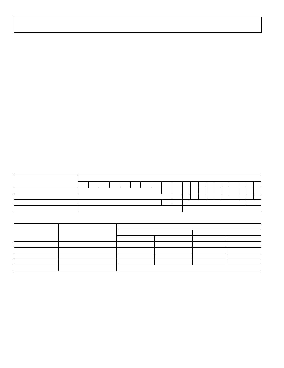
ADV7188
Rev. 0 | Page 72 of 112
PIXEL PORT CONFIGURATION
The ADV7188 has a very flexible pixel port that can be config-
ured in a variety of formats to accommodate downstream ICs.
Table 97 and Table 98 summarize the various functions that the
ADV7188 pins can have in different modes of operation.
The ordering of components, for example, Cr vs. Cb, CHA/B/C,
can be changed. Refer to the SWPC Swap Pixel Cr/Cb, Address
0x27 [7] section. Table 97 indicates the default positions for the
Cr/Cb components.
OF_SEL[3:0] Output Format Selection, Address 0x03 [5:2]
The modes in which the ADV7188 pixel port can be configured
are under the control of OF_SEL[3:0]. See Table 98 for details.
The default LLC frequency output on the LLC1 pin is approxi-
mately 27 MHz. For modes that operate with a nominal data
rate of 13.5 MHz (0001, 0010), the clock frequency on the LLC1
pin stays at the higher rate of 27 MHz. For information on
outputting the nominal 13.5 MHz clock on the LLC1 pin, see
the LLC_PAD_SEL[2:0] LLC1 Output Selection, Address 0x8F
[6:4] section.
SWPC Swap Pixel Cr/Cb, Address 0x27 [7]
0 (default)--No swapping is allowed.
1--The Cr and Cb values can be swapped.
LLC_PAD_SEL[2:0] LLC1 Output Selection, Address 0x8F [6:4]
The following I
2
C write allows the user to select between LLC1
(nominally at 27 MHz) and LLC2 (nominally at 13.5 MHz).
The LLC2 signal is useful for LLC2-compatible wide bus (16-/20-
bit) output modes. See the OF_SEL[3:0] Output Format Selection,
Address 0x03 [5:2] section for additional information. The LLC2
signal and data on the data bus are synchronized. By default, the
rising edge of LLC1/LLC2 is aligned with the Y data; the falling
edge occurs when the data bus holds C data. The polarity of the
clock, and therefore the Y/C assignments to the clock edges, can be
altered by using the Polarity LLC pin.
000 (default)--The output is nominally 27 MHz LLC on the
LLC1 pin.
101--The output is nominally 13.5 MHz LLC on the LLC1 pin.
Table 97. P19P0 Output/Input Pin Mapping
Data Port Pins P[19:0]
Processor, Format, and Mode
19 18 17 16 15 14 13 12 11 10 9 8 7 6 5 4 3 2 1 0
Video
Out,
8-Bit,
4:2:2
YCrCb[7:0]OUT
Video
Out,
10-Bit,
4:2:2
YCrCb[9:0]OUT
Video Out, 16-Bit, 4:2:2
Y[7:0]OUT
CrCb[7:0] OUT
Video Out, 20-Bit, 4:2:2
Y[9:0]OUT
CrCb[9:0] OUT
Table 98. Standard Definition Pixel Port Modes
Pixel Port Pins P[19:0]
P[19:10]
P9[9:0]
OF_SEL[3:0] Format
P[19:12] P[11:10] P[9:2] P[1:0]
0000
10-Bit at LLC1 4:2:2
YCrCb[9:2]
YCrCb[1:0]
Three-State
Three-State
0001
20-Bit at LLC2 4:2:2
Y[9:2]
Y[1:0]
CrCb[9:2]
CrCb[1:0]
0010
16-Bit at LLC2 4:2:2
Y[7:0]
Three-State
CrCb[7:0]
Three-State
0011 (default)
8-Bit at LLC1 4:2:2
YCrCb[7:0]
Three-State
Three-State
Three-State
0110-1111
Reserved
Reserved. Do not use.
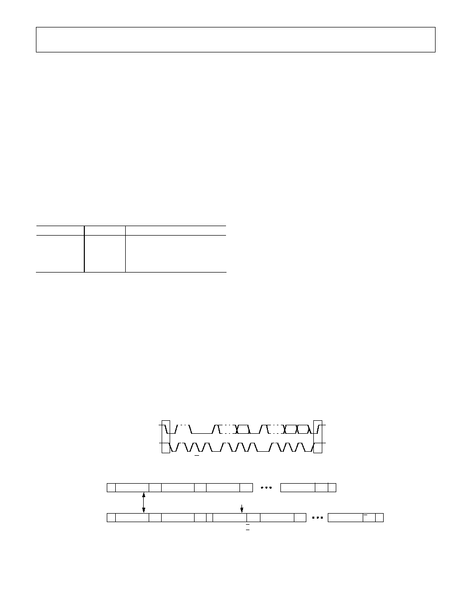
ADV7188
Rev. 0 | Page 73 of 112
MPU PORT DESCRIPTION
The ADV7188 supports a 2-wire (I
2
C-compatible) serial inter-
face. Two inputs, serial data (SDA) and serial clock (SCLK),
carry information between the ADV7188 and the system I
2
C
master controller. Each slave device is recognized by a unique
address. The ADV7188's I
2
C port allows the user to set up and
configure the decoder and to read back captured VBI data. The
ADV7188 has four possible slave addresses for both read and
write operations, depending on the logic level on the ALSB pin.
These four unique addresses are shown in Table 99. The
ADV7188's ALSB pin controls Bit 1 of the slave address. By
altering the ALSB, it is possible to control two ADV7188s in an
application without having a conflict with the same slave
address. The LSB (Bit 0) sets either a read or write operation.
Logic 1 corresponds to a read operation; Logic 0 corresponds to
a write operation.
Table 99. I
2
C Address
ALSB R/W
Slave
Address
0 0
0x40
0 1
0x41
1 0
0x42
1 1
0x43
To control the device on the bus, a specific protocol must be
followed. First, the master initiates a data transfer by
establishing a start condition, which is defined by a high-to-low
transition on SDA while SCLK remains high. This indicates that
an address/data stream follows. All peripherals respond to the
start condition and shift the next eight bits (7-bit address +
R/W bit). The bits are transferred from MSB down to LSB. The
peripheral that recognizes the transmitted address responds by
pulling the data line low during the ninth clock pulse; this is
known as an acknowledge bit. All other devices withdraw from
the bus at this point and maintain an idle condition. The idle
condition is where the device monitors the SDA and SCLK
lines, waiting for the start condition and the correct transmitted
address.
The R/W bit determines the direction of the data. Logic 0 on
the LSB of the first byte means the master writes information to
the peripheral. Logic 1 on the LSB of the first byte means the
master reads information from the peripheral.
The ADV7188 acts as a standard slave device on the bus. The
data on the SDA pin is eight bits long, supporting the 7-bit
addresses plus the R/W bit. The ADV7188 has 249 subaddresses
to enable access to the internal registers. It therefore interprets
the first byte as the device address and the second byte as the
starting subaddress. The subaddresses auto-increment, allowing
data to be written to or read from the starting subaddress. A
data transfer is always terminated by a stop condition. The user
can also access any unique subaddress register on a one-by-one
basis without updating all the registers.
Stop and start conditions can be detected at any stage during the
data transfer. If these conditions are asserted out of sequence with
normal read and write operations, they cause an immediate
jump to the idle condition. During a given SCLK high period,
the user should issue only one start condition, one stop condition,
or a single stop condition followed by a single start condition. If
an invalid subaddress is issued by the user, the ADV7188 does
not issue an acknowledge and returns to the idle condition.
If in autoincrement mode the highest subaddress is exceeded,
the following action is taken:
1.
In read mode, the highest subaddress register contents
continue to be output until the master device issues a no
acknowledge. This indicates the end of a read. In a no
acknowledge condition, the SDA line is not pulled low on
the ninth pulse.
2.
In write mode, the data for the invalid byte is not loaded
into any subaddress register, a no acknowledge is issued by
the ADV7188, and the part returns to the idle condition.
05478-049
SDATA
SCLOCK
START ADDR
ACK
ACK
DATA
ACK
STOP
SUBADDRESS
17
17
8
9
8
9
17
8
9
S
P
R/W
Figure 44. Bus Data Transfer
05478-050
S
WRITE
SEQUENCE
SLAVE ADDR A(S)
SUB ADDR
A(S)
DATA
A(S)
DATA
A(S) P
S
READ
SEQUENCE
SLAVE ADDR
SLAVE ADDR
A(S)
SUB ADDR
A(S) S
A(S)
DATA
A(M)
DATA
A(M) P
S = START BIT
P = STOP BIT
A(S) = ACKNOWLEDGE BY SLAVE
A(M) = ACKNOWLEDGE BY MASTER
A(S) = NO-ACKNOWLEDGE BY SLAVE
A(M) = NO-ACKNOWLEDGE BY MASTER
LSB = 1
LSB = 0
Figure 45. Read and Write Sequence
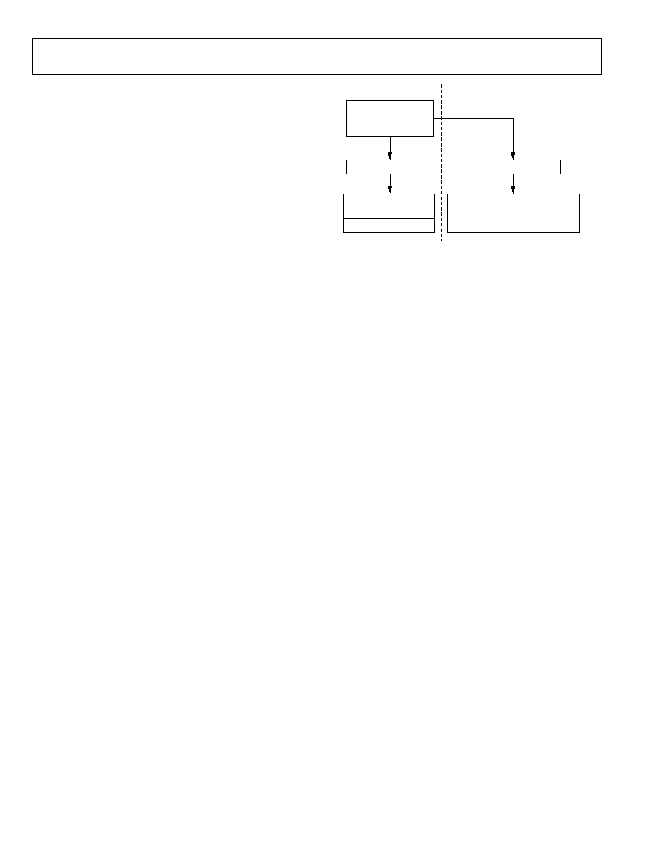
ADV7188
Rev. 0 | Page 74 of 112
REGISTER ACCESSES
The MPU can write to or read from most of the ADV7188's
registers, excepting the registers that are read only or write only.
The subaddress register determines which register the next read
or write operation accesses. All communications with the part
through the bus start with an access to the subaddress register.
A read/write operation is then performed from/to the target
address, which then increments to the next address until a stop
command on the bus is performed.
REGISTER PROGRAMMING
The I
2
C Register Maps section describes each register in terms
of its configuration. After the part has been accessed over the
bus and a read/write operation is selected, the subaddress is set
up. The subaddress register determines to/from which register
the operation takes place. Table 102 and Table 103 list the
various operations under the control of the subaddress register.
As can be seen in Figure 46, the registers in the ADV7188 are
arranged into two maps: the User Map (enabled by default) and
the User Sub Map. The User Sub Map has controls for the
interrupt and VDP functionality on the ADV7188 and the User
Map controls everything else.
The User Map and the User Sub Map consist of a common
space from address 0x00 to 0x3F. Depending on how Bit 5 in
register 0x0E (SUB_USR_EN) is set, the register map then splits
in two sections.
SUB_USR_EN, Address 0x0E [5]
This bit splits the register map at register 0x40.
0 (default)--The register map does not split and the User Map
is enabled.
1--The register map splits and the User Sub Map is enabled.
COMMON I
2
C SPACE
ADDRESS 0x00
0x3F
ADDRESS 0x0E BIT 5 = 0b
ADDRESS 0x0E BIT 5 = 1b
I
2
C SPACE
ADDRESS 0x40
0xFF
I
2
C SPACE
ADDRESS 0x40
0x9C
USER MAP
USER SUB MAP
NORMAL REGISTER SPACE
INTERRUPT AND VDP REGISTER SPACE
05478-048
Figure 46. Register Access --User Map and User Sub Map
I
2
C SEQUENCER
An I
2
C sequencer is used when a parameter exceeds eight bits,
and is therefore distributed over two or more I
2
C registers, for
example, HSB [11:0].
When such a parameter is changed using two or more I
2
C write
operations, the parameter may hold an invalid value for the
time between the first and last I
2
C being completed. In other
words, the top bits of the parameter may already hold the new
value while the remaining bits of the parameter still hold the
previous value.
To avoid this problem, the I
2
C sequencer holds the already
updated bits of the parameter in local memory; all bits of the
parameter are updated together once the last register write
operation has completed.
The correct operation of the I
2
C sequencer relies on the
following:
·
All I
2
C registers for the parameter in question must be
written to in order of ascending addresses. For example, for
HSB[10:0], write to Address 0x34 first, followed by 0x35.
·
No other I
2
C taking place between the two (or more) I
2
C
writes for the sequence. For example, for HSB[10:0], write
to Address 0x34 first immediately followed by 0x35.

ADV7188
Rev. 0 | Page 75 of 112
I
2
C REGISTER MAPS
USER MAP
The collective name for the registers in Table 100 below is the User Map.
Table 100. User Map Register Details
Address
Reset
Dec Hex Register Name
RW 7
6
5
4
3
2
1
0
Value
(Hex)
0 00 Input
Control
RW
VID_SEL.3
VID_SEL.2 VID_SEL.1 VID_SEL.0 INSEL.3 INSEL.2 INSEL.1 INSEL.0 00000000 00
1
01 Video Selection
RW
ENHSPLL
BETACAM
ENVSPROC
11001000 C8
3 03 Output
Control
RW
VBI_EN
TOD
OF_SEL.3
OF_SEL.2 OF_SEL.1 OF_SEL.0
SD_DUP_AV
00001100 0C
4 04
Extended Output
Control
RW BT656-4
TIM_OE
BL_C_VBI
EN_SFL_PIN
RANGE
01xx0101 45
7 07 Autodetect
Enable RW
AD_SEC525_EN
AD_SECAM_EN AD_N443_EN AD_P60_EN
AD_PALN_EN AD_PALM_EN AD_NTSC_EN AD_PAL_EN 01111111 7F
8 08 Contrast
RW
CON.7
CON.6
CON.5 CON.4 CON.3 CON.2 CON.1 CON.0 10000000 80
10
0A
Brightness RW
BRI.7 BRI.6 BRI.5
BRI.4 BRI.3 BRI.2 BRI.1 BRI.0
00000000 00
11 0B Hue
RW
HUE.7
HUE.6
HUE.5
HUE.4 HUE.3 HUE.2 HUE.1 HUE.0
00000000 00
12 0C Default
Value
Y
RW
DEF_Y.5
DEF_Y.4 DEF_Y.3 DEF_Y.2 DEF_Y.1 DEF_Y.0
DEF_VAL_AUTO
_EN
DEF_VAL_EN 00110110 36
13 0D Default
Value
C
RW
DEF_C.7 DEF_C.6 DEF_C.5
DEF_C.4 DEF_C.3 DEF_C.2 DEF_C.1 DEF_C.0
01111100 7C
14
0E
ADI
Control
SUB_USR_EN
00000000 00
15 0F
Power Management RW RES
PWRDN
PDBP
FB_PWRDN
00000000 00
16 10 Status
1
R COL_KILL
AD_RESULT.2 AD_RESULT.1 AD_RESULT.0 FOLLOW_PW FSC_LOCK LOST_LOCK IN_LOCK ---
---
18 12 Status 2
R
FSC NSTD
LL NSTD
MV AGC DET
MV PS DET
MVCS T3
MVCS DET
---
---
19 13 Status 3
R
PAL_SW_LOCK INTERLACE
STD FLD LEN FREE_RUN_ACT CVBS SD_OP_50Hz GEMD
INST_HLOCK ---
---
19 13
Analogue Control
Internal
W
XTAL_TTL_SEL
00000000 00
20 14
Analogue Clamp
Control
RW
CCLEN
00010010 12
21 15
Digital Clamp
Control 1
RW
DCT.1
DCT.0
0000xxxx 00
23 17
Shaping Filter
Control
RW CSFM.2
CSFM.1
CSFM.0
YSFM.4
YSFM.3 YSFM.2 YSFM.1 YSFM.0 00000001 01
24 18
Shaping Filter
Control 2
RW WYSFMOVR
WYSFM.4 WYSFM.3 WYSFM.2 WYSFM.1 WYSFM.0
10010011 93
25 19 Comb Filter Control RW
NSFSEL.1 NSFSEL.0 PSFSEL.1 PSFSEL.0
11110001 F1
29 1D ADI Control 2
RW TRI_LLC
EN28XTAL
00000xxx 00
39 27 Pixel Delay Control
RW SWPC
AUTO_PDC_EN CTA.2 CTA.1 CTA.0
LTA.1 LTA.0 01011000 58
43 2B Misc Gain Control
RW
CKE
PW_UPD
11100001 E1
44 2C AGC Mode Control
RW
LAGC.2
LAGC.1
LAGC.0
CAGC.1
CAGC.0
10101110 AE
45 2D
Chroma Gain Control
1
W CAGT.1
CAGT.0
CMG.11
CMG.10
CMG.9
CMG.8
11110100 F4
46 2E
Chroma Gain Control
2 W
CMG.7
CMG.6
CMG.5
CMG.4
CMG.3 CMG.2 CMG.1 CMG.0 00000000 00
47 2F
Luma Gain Control 1 W LAGT.1
LGAT.0
LMG.11
LMG.10
LMG.9
LMG.8
1111xxxx F0
48 30 Luma Gain Control 2 W LMG.7
LMG.6
LMG.5
LMG.4
LMG.3
LMG.2
LMG.1
LMG.0
xxxxxxxx 00
49 31
VSYNC Field Control
1
RW
NEWAVMODE HVSTIM
00010010 12
50 32
VSYNC Field Control
2
RW VSBHO
VSBHE
01000001 41
51 33
VSYNC Field Control
3
RW VSEHO
VSEHE
10000100 84
52 34
HSYNC Position
Control 1
RW
HSB.10
HSB.9
HSB.8
HSE.10
HSE.9
HSE.8
00000000 00
53 35
HSYNC Position
Control 2
RW HSB.7
HSB.6
HSB.5
HSB.4 HSB.3 HSB.2 HSB.1 HSB.0
00000010 02
54 36
HSYNC Position
Control 3
RW HSE.7
HSE.6
HSE.5
HSE.4 HSE.3 HSE.2 HSE.1 HSE.0
00000000 00
55 37 Polarity
RW PHS
PVS
PF
PCLK
00000001 01
56 38 NTSC Comb Control RW CTAPSN.1 CTAPSN.0 CCMN.2 CCMN.1 CCMN.0 YCMN.2 YCMN.1
YCMN.0 10000000 80
57 39 PAL Comb Control
RW CTAPSP.1
CTAPSP.0
CCMP.2 CCMP.1 CCMP.0 YCMP.2 YCMP.1 YCMP.0 11000000 C0
58
3A
ADC
Control
RW
PDN_ADC0 PDN_ADC1 PDN_ADC2 PDN_ADC3 00010001 11
61 3D
Manual Window
Control
RW
CKILLTHR.2
CKILLTHR.1
CKILLTHR.0
01000011 43
65 41 Resample Control
RW
SFL_INV
00000001 01
72 48 Gemstar Ctrl 1
RW GDECEL.15
GDECEL.14
GDECEL.13
GDECEL.12 GDECEL.11 GDECEL.10 GDECEL.9 GDECEL.8 00000000 00

ADV7188
Rev. 0 | Page 76 of 112
Address
Reset
Dec Hex Register Name
RW 7
6
5
4
3
2
1
0
Value
(Hex)
73 49 Gemstar Ctrl 2
RW GDECEL.7
GDECEL.6
GDECEL.5
GDECEL.4 GDECEL.3 GDECEL.2 GDECEL.1 GDECEL.0
00000000 00
74 4A Gemstar Ctrl 3
RW GDECOL.15
GDECOL.14
GDECOL.13
GDECOL.12 GDECOL.11 GDECOL.10 GDECOL.9 GDECOL.8 00000000 00
75 4B Gemstar Ctrl 4
RW GDECOL.7
GDECOL.6
GDECOL.5
GDECOL.4 GDECOL.3 GDECOL.2 GDECOL.1 GDECOL.0
00000000 00
76 4C Gemstar Ctrl 5
RW
GDECAD
xxxx0000 00
77 4D CTI DNR Ctrl 1
RW
DNR_EN
CTI_AB.1 CTI_AB.0 CTI_AB_EN CTI_EN 11101111 EF
78 4E CTI DNR Ctrl 2
RW CTI_C_TH.7
CTI_C_TH.6
CTI_C_TH.5
CTI_C_TH.4 CTI_C_TH.3 CTI_C_TH.2 CTI_C_TH.1 CTI_C_TH.0
00001000 08
80 50 CTI DNR Ctrl 4
RW DNR_TH.7
DNR_TH.6
DNR_TH.5
DNR_TH.4 DNR_TH.3 DNR_TH.2 DNR_TH.1 DNR_TH.0
00001000 08
81 51 Lock
Count
RW
FSCLE
SRLS
COL.2
COL.1
COL.0
CIL.2
CIL.1
CIL.0
00100100 24
143 8F
Free Run Line
Length 1
W
LLC_PAD_
SEL_MAN
LLC_PAD_
SEL.1
LLC_PAD_
SEL.0
00000000 00
153 99 CCAP 1
R CCAP1.7
CCAP1.6
CCAP1.5
CCAP1.4 CCAP1.3 CCAP1.2 CCAP1.1 CCAP1.0
--- ---
154 9A CCAP 2
R CCAP2.7
CCAP2.6
CCAP2.5
CCAP2.4 CCAP2.3 CCAP2.2 CCAP2.1 CCAP2.0
--- ---
155 9B Letterbox 1
R LB_LCT.7 LB_LCT.6 LB_LCT.5
LB_LCT.4 LB_LCT.3 LB_LCT.2 LB_LCT.1 LB_LCT.0 --- ---
156 9C Letterbox 2
R LB_LCM.7 LB_LCM.6 LB_LCM.5
LB_LCM.4 LB_LCM.3 LB_LCM.2 LB_LCM.1 LB_LCM.0 --- ---
157 9D Letterbox 3
R LB_LCB.7 LB_LCB.6 LB_LCB.5
LB_LCB.4 LB_LCB.3 LB_LCB.2 LB_LCB.1 LB_LCB.0 --- ---
195 C3 ADC Switch 1
RW ADC1_SW.3
ADC1_SW.2
ADC1_SW.1
ADC1_SW.0 ADC0_SW.3 ADC0_SW.2 ADC0_SW.1 ADC0_SW.0
xxxxxxxx
00
196 C4 ADC Switch 2
RW ADC_SW_MAN
ADC2_SW.3
ADC2_SW.2
ADC2_SW.1
ADC2_SW.0
0xxxxxxx 00
220 DC Letterbox Control 1
RW
LB_TH.4
LB_TH.3
LB_TH.2
LB_TH.1
LB_TH.0
10101100 AC
221 DD Letterbox Control 2
RW LB_SL.3 LB_SL.2 LB_SL.1
LB_SL.0 LB_EL.3 LB_EL.2 LB_EL.1 LB_EL.0 01001100 4C
222 DE ST Noise Readback 1 R
ST_NOISE_VLD ST_NOISE.10 ST_NOISE.9 ST_NOISE.8 ---
---
223 DF ST Noise Readback 2 R
ST_NOISE.7
ST_NOISE.6
ST_NOISE.5
ST_NOISE.4 ST_NOISE.3 ST_NOISE.2 ST_NOISE.1 ST_NOISE.0
---
---
225 E1 SD Offset Cb
RW SD_OFF_CB.7
SD_OFF_CB.6
SD_OFF_CB.5 SD_OFF_CB.4 SD_OFF_CB.3 SD_OFF_CB.2 SD_OFF_CB.1 SD_OFF_CB.0 10000000 80
226 E2 SD Offset Cr
RW SD_OFF_CR.7
SD_OFF_CR.6 SD_OFF_CR.5 SD_OFF_CR.4 SD_OFF_CR.3 SD_OFF_CR.2 SD_OFF_CR.1 SD_OFF_CR.0 10000000 80
227 E3 SD Saturation CB
RW SD_SAT_CB.7
SD_SAT_CB.6
SD_SAT_CB.5 SD_SAT_CB.4 SD_SAT_CB.3 SD_SAT_CB.2 SD_SAT_CB.1 SD_SAT_CB.0 10000000 80
228 E4 SD Saturation Cr
RW SD_SAT_CR.7
SD_SAT_CR.6
SD_SAT_CR.5 SD_SAT_CR.4 SD_SAT_CR.3 SD_SAT_CR.2 SD_SAT_CR.1 SD_SAT_CR.0 10000000 80
229 E5 NTSC V bit begin
RW NVBEGDELO NVBEGDELE NVBEGSIGN NVBEG.4
NVBEG.3 NVBEG.2 NVBEG.1 NVBEG.0 00100101 25
230 E6 NTSC V bit end
RW NVENDDELO
NVENDDELE
NVENDSIGN NVEND.4
NVEND.3
NVEND.2 NVEND.1 NVEND.0 00000100 04
231 E7 NTSC F bit toggle
RW NFTOGDELO NFTOGDELE NFTOGSIGN NFTOG.4
NFTOG.3 NFTOG.2 NFTOG.1 NFTOG.0 01100011 63
232 E8 PAL V bit begin
RW PVBEGDELO
PVBEGDELE
PVBEGSIGN PVBEG.4
PVBEG.3
PVBEG.2 PVBEG.1 PVBEG.0 01100101 65
233 E9 PAL V bit end
RW PVENDDELO
PVENDDELE
PVENDSIGN PVEND.4
PVEND.3
PVEND.2
PVEND.1
PVEND.0
00010100 14
234 EA PAL F bit toggle
RW PFTOGDELO
PFTOGDELE
PFTOGSIGN PFTOG.4
PFTOG.3
PFTOG.2 PFTOG.1 PFTOG.0 01100011 63
235 EB Vblank Control 1
RW NVBIOLCM.1
NVBIOLCM.0 NVBIELCM.1 NVBIELCM.0 PVBIOLCM.1 PVBIOLCM.0 PVBIELCM.1 PVBIELCM.0 01010101 55
236 EC Vblank Control 2
RW NVBIOCCM.1
NVBIOCCM.0
NVBIECCM.1
NVBIECCM.0 PVBIOCCM.1 PVBIOCCM.0 PVBIECCM.1 PVBIECCM.0 01010101 55
237 ED FB_STATUS
R FB_STATUS.3 FB_STATUS.2
FB_STATUS.1 FB_STATUS.0
---
---
237 ED FB_CONTROL1
W
FB_INV CVBS_RGB_SEL FB_MODE.1
FB_MODE.0
00010000 10
238 EE FB_CONTROL 2
RW FB_CSC_MAN
MAN_ALPHA_
VAL.6
MAN_ALPHA_
VAL.5
MAN_ALPHA_
VAL.4
MAN_ALPHA_
VAL.3
MAN_ALPHA_
VAL.2
MAN_ALPHA_
VAL.1
MAN_ALPHA_
VAL.0
00000000 00
239 EF FB_CONTROL 3
RW
FB_SP_
ADJUST.3
FB_SP_
ADJUST.2
FB_SP_
ADJUST.1
FB_SP_
ADJUST.0
CNTR_
ENABLE
FB_EDGE_
SHAPE.2
FB_EDGE_
SHAPE.1
FB_EDGE_
SHAPE.0 01001010 4A
240 F0
FB_CONTROL 4
RW
FB_DELAY.3 FB_DELAY.2 FB_DELAY.1 FB_DELAY.0 01000100 44
241 F1 FB_CONTROL 5
RW CNTR_LEVEL.1 CNTR_LEVEL.0 FB_LEVEL.1 FB_LEVEL.0 CNTR_MODE.1 CNTR_MODE.0
RGB_IP_SEL
00001100 0C
243 F3 AFE_CONTROL 1
RW ADC3_SW.3
ADC3_SW.2
ADC3_SW.1 ADC3_SW.0 AA_FILT_EN.3
AA_FILT_EN.2
AA_FILT_EN.1 AA_FILT_EN.0 00000000 00
244 F4
Drive Strength
RW
DR_STR
DR_STR.0
DR_STR_C DR_STR_C.0
DR_STR_S DR_STR_S.0
xx010101 15
248 F8
IF Comp Control
RW
IFFILTSEL.2
IFFILTSEL.1
IFFILTSEL.0
00000000 00
249 F9
VS Mode Control
RW
VS_COAST_
MODE.1
VS_COAST_
MODE.0
EXTEND_VS_
MIN_FREQ
EXTEND_VS_
MAX_FREQ 00000000 00
251 FB Peaking Control
RW
PEAKING_
GAIN.7
PEAKING_
GAIN.6
PEAKING_
GAIN.5
PEAKING_
GAIN.4
PEAKING_
GAIN.3
PEAKING_
GAIN.2
PEAKING_
GAIN.1
PEAKING_
GAIN.0 01000000 40
252 FC Coring Threshold 2
RW DNR_TH_2.7
DNR_TH_2.6
DNR_TH_2.5
DNR_TH_2.4 DNR_TH_2.3 DNR_TH_2.2 DNR_TH_2.1 DNR_TH_2.0
00000100 04
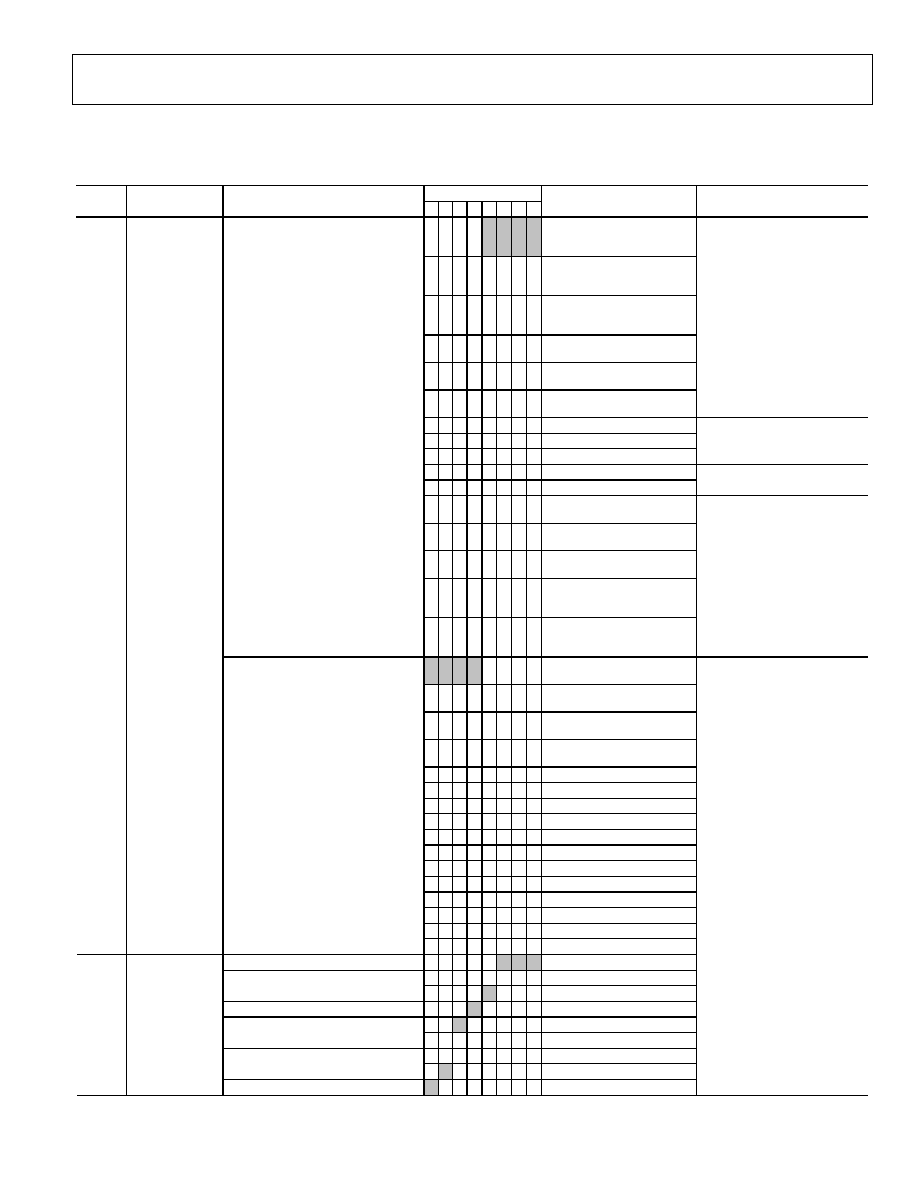
ADV7188
Rev. 0 | Page 77 of 112
Table 101 provides a detailed description of the registers located in the User Map.
Table 101. User Map Detailed Description
Bit
Address
Register
Bit Description
7 6 5 4 3 2 1 0 Comments Notes
0 0 0 0 CVBS in on AIN1, SCART: G on
AIN6/AIN9, B on AIN4/AIN7, R on
AIN5/AIN8
0 0 0 1 CVBS in on AIN2, SCART: G on
AIN6/AIN9, B on AIN4/AIN7, R on
AIN5/AIN8
0 0 1 0 CVBS in on AIN3, SCART: G on
AIN6/AIN9, B on AIN4/AIN7, R on
AIN5/AIN8
0 0 1 1 CVBS in on AIN4, SCART: G on
AIN9, B on AIN7, R on AIN8
0 1 0 0 CVBS in on AIN5, SCART: G on
AIN9, B on AIN7, R on AIN8
0 1 0 1 CVBS in on AIN6, SCART: G on
AIN9, B on AIN7, R on AIN8
Composite and SCART RGB (RGB
analog input options selectable via
RGB_IP_SEL)
0 1 1 0 Y on AIN1, C on AIN4
0 1 1 1 Y on AIN2, C on AIN5
1 0 0 0 Y on AIN3, C on AIN6
S-Video
1 0 0 1 Y on AIN1, Pb on AIN4, Pr on AIN5
0x00
Input Control
1 0 1 0 Y on AIN2, Pb on AIN3, Pr on AIN6
YpbPr
1 0 1 1 CVBS in on AIN7, SCART: G on
AIN6, B on AIN4, R on AIN5
1 1 0 0 CVBS in on AIN8, SCART: G on
AIN6, B on AIN4, R on AIN5
1 1 0 1 CVBS in on AIN9, SCART: G on
AIN6, B on AIN4, R on AIN5
1 1 1 0 CVBS in on AIN10, SCART: G on
AIN6 / AIN9, B on AIN4 / AIN7, R on
AIN5 / AIN8
INSEL [3:0]. The INSEL bits allow the user to
select an input channel and the input format.
1 1 1 1 CVBS in on AIN11, SCART: G on
AIN6 / AIN9, B on AIN4 / AIN7, R on
AIN5 / AIN8
Composite & SCART RGB (RGB analog
input options selectable via
RGB_IP_SEL)
0 0 0 0 Auto-detect
PAL
(BGHID),
NTSC
(without pedestal), SECAM
0 0 0 1 Auto-detect PAL (BGHID), NTSC
(M) (with pedestal), SECAM
0 0 1 0 Auto-detect PAL (N), NTSC (M)
(without pedestal), SECAM
0 0 1 1 Auto-detect PAL (N), NTSC (M)
(with pedestal), SECAM
0 1 0 0 NTSC(J)
VID_SEL [3:0]. The VID_SEL bits allow the user
to select the input video standard.
0 1 0 1 NTSC(M)
0 1 1 0 PAL 60
0 1 1 1 NTSC 4.43
1 0 0 0 PAL BGHID
1 0 0 1 PAL N (BGHID without pedestal)
1 0 1 0 PAL M (without pedestal)
1 0 1 1 PAL M
1 1 0 0 PAL combination N
1 1 0 1 PAL combination N
1 1 1 0 SECAM (with pedestal)
1 1 1 1 SECAM (with pedestal)
Reserved.
0 0 0 Set to default
0
Disable VSYNC processor
ENVSPROC
1 Enable
VSYNC
processor
Reserved.
0 Set
to
default
0
Standard video input
BETACAM
1
Betacam input enable
0
Disable HSYNC processor
ENHSPLL
1
Enable HSYNC processor
0x01 Video
Selection
Reserved.
1 Set
to
default
ADV7188
Rev. 0 | Page 78 of 112
Bit
Address
Register
Bit Description
7 6 5 4 3 2 1 0 Comments Notes
0 AV codes to suit 8-bit interleaved
data output
SD_DUP_AV. Duplicates the AV codes from
the luma into the chroma path.
1 AV codes duplicated (for 16-bit
interfaces)
Reserved.
0
Set as default
0 0 0 0
Reserved
0 0 0 1
Reserved
0 0 1 0
16-bit @ LLC1 4:2:2
0 0 1 1
8-bit @ LLC1 4:2:2 ITU-R BT.656
0 1 0 0
Not used
0 1 0 1
Not used
0 1 1 0
Not used
0 1 1 1
Not used
1 0 0 0
Not used
1 0 0 1
Not used
1 0 1 0
Not used
1 0 1 1
Not used
1 1 0 0
Not used
1 1 0 1
Not used
1 1 1 0
Not used
OF_SEL [3:0]. Allows the user to choose from
a set of output formats.
1 1 1 1
Not used
0 Output
pins
enabled
TOD. Three-state output drivers. This bit
allows the user to three-state the output
drivers: P[19:0], HS, VS, FIELD, and SFL.
1 Drivers
three-stated
See also TIM_OE and TRI_LLC
0 All
lines
filtered
and
scaled
0x03 Output
Control
VBI_EN. Allows VBI data (Lines 1 to 21) to be
passed through with only a minimum
amount of filtering performed.
1 Only
active
video
region
filtered
0 16 < Y < 235, 16 < C < 240
ITU-R BT.656
RANGE. Allows the user to select the range of
output values. Can be BT656 compliant, or
can fill the whole accessible number range.
1 1 < Y < 254, 1 < C < 254
Extended range
0
SFL output is disabled
EN_SFL_PIN
1
SFL information output on the SFL
pin
SFL output enables connecting
encoder and decoder directly
0 Decode
and
output
color
BL_C_VBI. Blank chroma during VBI. If set,
enables data in the VBI region to be passed
through the decoder undistorted.
1
Blank Cr and Cb
During VBI
0 HS,
VS,
F
three-stated
TIM_OE. Timing signals output enable.
1
HS, VS, F forced active
Controlled by TOD
Reserved.
x x
Reserved.
1
0
BT656-3-complatible
0x04 Extended
Output
Control
BT656-4. Allows the user to select
an output mode-compatible with
ITU- R BT656-3/4.
1
BT656-4-compatible
0 Disable
AD_PAL_EN. PAL B/G/I/H autodetect enable.
1 Enable
0
Disable
AD_NTSC_EN. NTSC autodetect enable.
1 Enable
0
Disable
AD_PALM_EN. PAL M autodetect enable.
1 Enable
0
Disable
AD_PALN_EN. PAL N autodetect enable.
1 Enable
0
Disable
AD_P60_EN. PAL 60 autodetect enable.
1
Enable
0
Disable
AD_N443_EN. NTSC443 autodetect enable.
1
Enable
0
Disable
AD_SECAM_EN. SECAM autodetect enable.
1
Enable
0
Disable
0x07 AutodetectEnable
AD_SEC525_EN. SECAM 525 autodetect
enable.
1
Enable
0x08
Contrast Register
CON[7:0]. Contrast adjust. This is the user
control for contrast adjustment.
1 0 0 0 0 0 0 0 Luma gain = 1
0x00 Gain = 0;
0x80 Gain = 1;
0xFF Gain = 2
0x09 Reserved
Reserved.
1 0 0 0 0 0 0 0
0x0A
Brightness Register
BRI[7:0]. This register controls the brightness
of the video signal.
0 0 0 0 0 0 0 0
0x00 = 0mV
0x7F = +204mV
ADV7188
Rev. 0 | Page 79 of 112
Bit
Address
Register
Bit Description
7 6 5 4 3 2 1 0 Comments Notes
0x80 = -204mV
0x0B
Hue Register
HUE[7:0]. This register contains the value for
the color hue adjustment.
0 0 0 0 0 0 0 0
Hue range = 90° to +90°
0 Free-run mode dependent on
DEF_VAL_AUTO_EN
DEF_VAL_EN. Default value enable.
1 Force free-run mode on and
output blue screen
0 Disable
free-run
mode
DEF_VAL_AUTO_EN. Default value.
1
Enable automatic free-run mode
(blue screen)
When lock is lost, free-run mode can
be enabled to output stable timing,
clock, and a set color.
0 0 1 1 0 1
0x0C Default
Value
Y
DEF_Y[5:0]. Default value Y. This register
holds the Y default value.
Y[7:0] = {DEF_Y[5:0],0, 0}
Default Y value output in free-run
mode.
0 1 1 1 1 1 0 0
0x0D Default
Value
C DEF_C[7:0].
Default value C. The Cr and Cb
default values are defined in this register.
Cr[7:0] = DEF_C[7:4],0, 0, 0, 0}
Cb[7:0] = DEF_C[3:0], 0, 0, 0, 0}
Default Cb/Cr value output in free-run
mode. Default values give blue screen
output.
Reserved.
0 0 0 0 0 Set as default
0
Access User Map
SUB_USR_EN. Enables the user to access the
User Sub Map
1
Access User Sub Map
See Figure 46
0x0E ADI
Control
Reserved.
0 0
Set as default
Reserved.
0 Set to default
0
FB input operational
FB_PWRDN
1
FB input in power save mode
0 Chip
power-down
controlled
by
pin
PDBP. Power-down bit priority selects
between PWRDN bit or pin.
1 Bit
has
priority
(pin
disregarded)
Reserved.
0 0 Set
to
default
0
System functional
PWRDN. Power-down places the decoder in a
full power-down mode.
1 Powered
down
See
PDBP,
0x0F
Bit
2
Reserved.
0 Set
to
default
0
Normal operation
0x0F Power
Management
RES. Chip Reset loads all I
2
C bits with default
values.
1 Start
reset
sequence
Executing
reset
takes
approx.
2
ms.
Self-clearing.
IN_LOCK
x In lock (right now) = 1
LOST_LOCK
x
Lost
lock
(since
last
read)
=
1
FSC_LOCK
x
Fsc
lock
(right
now)
=
1
FOLLOW_PW
x
Peak white AGC mode active = 1
Provides information about the
internal status of the decoder.
0 0 0
NTSM-MJ
0 0 1 NTSC-443
0 1 0
PAL-M
0 1 1
PAL-60
1 0 0
PAL-BGHID
1 0 1
SECAM
1 1 0
PAL combination N
AD_RESULT[2:0]. Autodetection result
reports the standard of the Input video.
1 1 1 SECAM
525
Detected standard
0x10
Status Register 1
(Read Only)
COL_KILL
x
Color kill is active = 1
Color kill
0x11
IDENT (Read Only)
IDENT[7:0] Provides identification on the
revision of the part.
x x x x x x x x
MVCS DET
x MV color striping detected
1 = Detected
MVCS T3
x
MV color striping type
0 = Type 2; 1 = Type 3
MV_PS DET
x
MV pseudo Sync detected
1 = Detected
MV_AGC DET
x
MV AGC pulses detected
1 = Detected
LL_NSTD
x Nonstandard
line
length
1
=
Detected
FSC_NSTD
x Fsc
frequency
nonstandard
1
=
Detected
0x12
Status Register 2
(Read Only)
Reserved.
x x
INST_HLOCK
x 1
=
horizontal
lock
achieved
Unfiltered
GEMD
x
1 = Gemstar data detected
When GEMD bit goes HIGH, it will
remain HIGH until end of active video
lines in that field.
SD_OP_50HZ
x
SD field rate detect
0 = SD 60 Hz detected;
1 = SD 50 Hz detected
CVBS
x
Result of CVBS/YC autodetection
0 = Y/C; 1 = CVBS
FREE_RUN_ACT
x
1 = Free-run mode active
Blue screen output
STD FLD_LEN
x
1 = Field length standard
Correct field length found
0x13
Status Register 3
(Read only)
INTERLACED
x
1 = Interlaced video detected
Field sequence found
ADV7188
Rev. 0 | Page 80 of 112
Bit
Address
Register
Bit Description
7 6 5 4 3 2 1 0 Comments Notes
PAL_SW_LOCK
x
1 = Swinging burst detected
Reliable swinging burst sequence
Reserved.
0 0
0
Crystal used to derive
28.63636 MHz clock
XTAL_TTL_SEL
1 External
TTL
level
clock
supplied
0x13 Analogue
Control
Internal (Write Only)
Reserved.
0 0 0 0 0
Reserved.
0 0 1 0 Set to default
0 Current
sources
switched
off
CCLEN. Current clamp enable allows the user
to switch off the current sources in the
analog front.
1 Current
sources
enabled
0x14 Analog
Clamp
Control
Reserved.
0 0 0 Set
to
default
Reserved.
0 x x x x Set to default
0 0
Slow (TC = 1 sec)
0 1
Medium (TC = 0.5 sec)
1 0
Fast (TC = 0.1 sec)
DCT[1:0]. Digital clamp timing determines
the time constant of the digital fine clamp
circuitry.
1 1
TC dependent on video
0x15 Digital
Clamp
Control 1
Reserved.
0 Set
to
default
0 0 0 0 0 Auto wide notch for poor quality
sources or wide-band filter with
Comb for good quality input
0 0 0 0 1 Auto narrow notch for poor
quality sources or wideband filter
with comb for good quality input
Decoder selects optimum Y-shaping
filter depending on CVBS quality.
0 0 0 1 0 SVHS 1
0 0 0 1 1 SVHS 2
0 0 1 0 0 SVHS 3
0 0 1 0 1 SVHS 4
0 0 1 1 0 SVHS 5
0 0 1 1 1 SVHS 6
0 1 0 0 0 SVHS 7
0 1 0 0 1 SVHS 8
0 1 0 1 0 SVHS 9
0 1 0 1 1 SVHS 10
0 1 1 0 0 SVHS 11
0 1 1 0 1 SVHS 12
0 1 1 1 0 SVHS 13
0 1 1 1 1 SVHS 14
1 0 0 0 0 SVHS 15
1 0 0 0 1 SVHS 16
1 0 0 1 0 SVHS 17
0x17 Shaping
Filter
Control
1 0 0 1 1 SVHS 18 (CCIR601)
1 0 1 0 0 PAL NN1
1 0 1 0 1 PAL NN2
1 0 1 1 0 PAL NN3
1 0 1 1 1 PAL WN 1
1 1 0 0 0 PAL WN 2
1 1 0 0 1 NTSC NN1
1 1 0 1 0 NTSC NN2
1 1 0 1 1 NTSC NN3
1 1 1 0 0 NTSC WN1
1 1 1 0 1 NTSC WN2
1 1 1 1 0 NTSC WN3
YSFM[4:0]. Selects Y-shaping filter mode
when in CVBS only mode.
Allows the user to select a wide range of low-
pass and notch filters.
If either auto mode is selected, the decoder
selects the optimum Y filter depending on
the CVBS video source quality (good vs. bad).
1 1 1 1 1 Reserved
If one of these modes is selected, the
decoder does not change filter modes.
Depending on video quality, a fixed
filter response (the one selected) is
used for good and bad quality video.
0x17
Shaping Filter
0 0 0 Auto
selection
15
MHz
Control (cont.)
0 0 1 Auto selection 2.17 MHz
Automatically selects a C filter based
on video standard and quality.
0 1 0 SH1
0 1 1 SH2
1 0 0 SH3
1 0 1 SH4
1 1 0 SH5
CSFM[2:0].
C-shaping filter mode allows the selection
from a range of low-pass chrominance filters.
If either auto mode is selected, the decoder
selects the optimum C filter depending on
the CVBS video source quality (good vs. bad).
Non-auto settings force a C filter for all
standards and quality of CVBS video.
1 1 1 Wideband mode
Selects a C filter for all video standards
and for good and bad video.
0 0 0 0 0 Reserved. Do not use.
0 0 0 0 1 Reserved. Do not use.
0 0 0 1 0 SVHS 1
0 0 0 1 1 SVHS 2
0x18 Shaping
Filter
Control 2
WYSFM[4:0]. Wideband Y-shaping filter
mode allows the user to select which Y-
shaping filter is used for the Y component of
Y/C, YPbPr, B/W input signals; it is also used
when a good quality input CVBS signal is
detected. For all other inputs, the Y-shaping
0 0 1 0 0 SVHS 3
ADV7188
Rev. 0 | Page 81 of 112
Bit
Address
Register
Bit Description
7 6 5 4 3 2 1 0 Comments Notes
0 0 1 0 1 SVHS 4
0 0 1 1 0 SVHS 5
0 0 1 1 1 SVHS 6
0 1 0 0 0 SVHS 7
0 1 0 0 1 SVHS 8
0 1 0 1 0 SVHS 9
0 1 0 1 1 SVHS 10
0 1 1 0 0 SVHS 11
0 1 1 0 1 SVHS 12
0 1 1 1 0 SVHS 13
0 1 1 1 1 SVHS 14
1 0 0 0 0 SVHS 15
1 0 0 0 1 SVHS 16
1 0 0 1 0 SVHS 17
1 0 0 1 1 SVHS 18 (CCIR 601)
1 0 1 0 0 Reserved. Do not use.
~ ~ ~ ~ ~ Reserved. Do not use.
filter chosen is controlled by YSFM[4:0].
1 1 1 1 1 Reserved. Do not use.
Reserved.
0 0 Set
to
default
0 Auto
selection
of
best
filter
WYSFMOVR. Enables the use of automatic
WYSFN filter.
1 Manual
select
filter
using
WYSFM[4:0]
0 0 Narrow
0 1 Medium
1 0 Wide
PSFSEL[1:0]. Controls the signal bandwidth
that is fed to the comb filters (PAL).
1 1 Widest
0 0 Narrow
0 1
Medium
1 0
Medium
NSFSEL[1:0]. Controls the signal bandwidth
that is fed to the comb filters (NTSC).
1 1
Wide
0x19
Comb Filter Control
Reserved.
1 1 1 1 Set
as
default
Reserved.
0 0 0 x x x Set to default
0
Use 27 MHz crystal
EN28XTAL
1 Use
28.63636
MHz
crystal
0
LLC pin active
0x1D
ADI Control 2
TRI_LLC
1
LLC pin three-stated
0 0 No Delay
1 0 Luma
1
clk
(37
nS)
delayed
1 0 Luma
2
clk
(74
nS)
early
LTA[1:0]. Luma timing adjust allows the user
to specify a timing difference between
chroma and luma samples.
1 1 Luma
1
clk
(37
nS)
early
CVBS mode LTA[1:0] = 00b
S-Video mode LTA[1:0]= 01b
YPrPb mode LTA[1:0] = 01b
Reserved.
0 Set
to
Zero
0 0 0 Not
valid
setting
0 0 1 Chroma
+
2
pixels
(early)
0 1 0
Chroma + 1 pixel (early)
0 1 1 No
delay
1 0 0
Chroma - 1 pixel (late)
1 0 1 Chroma
-
2
pixels
(late)
1 1 0 Chroma
-
3
pixels
(late)
CTA[2:0]. Chroma timing adjust allows a
specified timing difference between the
luma and chroma samples.
1 1 1 Not
valid
setting
CVBS mode CTA[2:0] = 011b
S-Video mode CTA[2:0] = 101b
YPrPb mode CTA[2:0] = 110b
0
Use values in LTA[1:0] and
CTA[2:0] for delaying
luma/chroma
AUTO_PDC_EN. Automatically programs the
LTA/CTA values to align luma and chroma at
the output for all modes of operation.
1
LTA and CTA values determined
automatically
0
No Swapping
0x27
Pixel Delay Control
SWPC. Allows the Cr and Cb samples to be
swapped.
1
Swap the Cr and Cb O/P samples
0 Update once per video line
PW_UPD. Peak white update determines the
rate of gain.
1 Update once per field
Peak white must be enabled. See
LAGC[2:0]
Reserved.
1 0 0 0 0
Set to default
0 Color
kill
disabled
CKE. Color kill enable allows the color kill
function to be switched on and off.
1 Color
kill
enabled
For SECAM color kill, threshold is set at
8%. See CKILLTHR[2:0]
0x2B
Misc Gain Control
Reserved.
1 Set
to
default
ADV7188
Rev. 0 | Page 82 of 112
Bit
Address
Register
Bit Description
7 6 5 4 3 2 1 0 Comments Notes
0 0 Manual
fixed
gain
Use
CMG[11:0]
0 1 Use
luma
gain
for
chroma
1 0 Automatic gain
Based on color burst
CAGC[1:0]. Chroma automatic gain control
selects the basic mode of operation for the
AGC in the chroma path.
1 1 Freeze
chroma
gain
Reserved.
1 1 Set
to
1
0 0 0 Manual
fixed
gain
Use
LMG[11:0]
0 0 1
AGC Peak white algorithm off
Blank level to sync tip
0 1 0
AGC Peak white algorithm on
Blank level to sync tip
0 1 1
Reserved
1 0 0
Reserved
1 0 1
Reserved
1 1 0
Reserved
LAGC[2:0]. Luma automatic gain control
selects the mode of operation for the gain
control in the luma path.
1 1 1 Freeze
gain
0x2C
AGC Mode Control
Reserved.
1
Set to 1
CMG[11:8]. Chroma manual gain can be used
to program a desired manual chroma gain.
Reading back from this register in AGC mode
gives the current gain.
0 1 0 0
CAGC[1:0] settings decide in which
mode CMG[11:0] operates
Reserved.
1 1 Set
to
1
0 0
Slow (TC = 2 s)
0 1
Medium (TC = 1 s)
1 0
Fast (TC = 0.2 s)
0x2D Chroma
Gain
Control 1
CAGT[1:0]. Chroma automatic gain timing
allows adjustment of the chroma AGC
tracking speed.
1 1
Adaptive
Has an effect only if CAGC[1:0] is set to
auto gain (10)
0x2E Chroma
Gain
Control 2
CMG[7:0]. Chroma manual gain lower 8 bits.
See CMG[11:8] for description.
0 0 0 0 0 0 0 0 CMG[11:0] = 750d; gain is 1 in
NTSC
CMG[11:0] = 741d; gain is 1 in PAL
Min value is 0d (G = 60 dB)
Max value is 3750 (G = 5)
LMG[11:8]. Luma manual gain can be used to
program a desired manual chroma gain, or to
read back the actual gain value used.
x x x x LAGC[1:0] settings decide in which
mode LMG[11:0] operates
Reserved.
1 1 Set
to
1
0 0
Slow (TC = 2 s)
0 1
Medium (TC = 1 s)
1 0
Fast (TC = 0.2 s)
0x2F
Luma Gain Control 1
LAGT[1:0]. Luma automatic gain timing
allows adjustment of the luma AGC tracking
speed.
1 1
Adaptive
Only has an effect if LAGC[1:0] is set to
auto gain (001, 010, 011,or 100)
0x30
Luma Gain Control 2 LMG[7:0]. Luma manual gain can be used to
program a desired manual chroma gain or
read back the actual used gain value.
x x x x x x x x LMG[11:0] = 1128 dec; gain is 1 in
NTSC LMG[11:0] = 1222d; gain is 1
in PAL
Min value NTSC 1024 (G = 0.90) PAL (G
= 0.84)
Max value NTSC 4095 (G = 3.63),
PAL = 4095 (G = 3.35)
Reserved.
0 1 0 Set to default
0
Start of line relative to HSE
HSE = HSYNC end
HVSTIM. Selects where within a line of video
the VS signal is asserted.
1
Start of line relative to HSB
HSB = HSYNC begin
0 EAV/SAV
codes
generated
to
suit
ADI encoders
NEWAVMODE. Sets the EAV/SAV mode.
1
Manual VS/Field position
controlled by Registers 0x32, 0x33,
and 0xE50xEA
0x31
VS and FIELD
Control 1
Reserved.
0 0 0 Set
to
default
Reserved.
0 0 0 0 0 1 Set to default
0
VS goes high in the middle of the
line (even field)
VSBHE
1
VS changes state at the start of the
line (even field)
0
VS goes high in the middle of the
line (odd field)
0x32
VSYNC Field Control
2
VSBHO
1
VS changes state at the start of the
line (odd field)
NEWAVMODE bit must be set high.
Reserved.
0 0 0 1 0 0 Set to default
0
VS goes low in the middle of the
line (even field)
VSEHE
1
VS changes state at the start of the
line (even field)
0
VS goes low in the middle of the
line (odd field)
0x33
VSYNC Field Control
3
VSEHO
1
VS changes state at the start of the
line odd field
NEWAVMODE bit must be set high.
ADV7188
Rev. 0 | Page 83 of 112
Bit
Address
Register
Bit Description
7 6 5 4 3 2 1 0 Comments Notes
HSE[10:8]. HS end allows the positioning of
the HS output within the video line.
0 0 0 HS output ends HSE[10:0] pixels
after the falling edge of HSYNC
Using HSB and HSE the user can
program the position and length of
the output HSYNC
Reserved.
0 Set
to
0
HSB[10:8]. HS begin allows the positioning of
the HS output within the video line.
0 0 0 HS
output
starts
HSB[10:0]
pixels
after the falling edge of HSYNC
0x34
HS Position Control
1
Reserved.
0
Set to 0
0x35
HS Position Control
2
HSB[7:0]. See above, using HSB[10:0] and
HSE[10:0], the user can program the position
and length of HS output signal.
0 0 0 0 0 0 1 0
0x36
HS Position Control
3
HSE[7:0]. See above.
0 0 0 0 0 0 0 0
0 Invert polarity
PCLK. Sets the polarity of LLC1.
1 Normal polarity as per the timing
diagrams
Reserved.
0 0
Set to 0
0 Active high
PF. Sets the FIELD polarity.
1
Active low
Reserved.
0 Set
to
0
0
Active high
PVS. Sets the VS Polarity.
1
Active low
Reserved.
0
Set to 0
0
Active high
0x37 Polarity
PHS. Sets HS Polarity.
1
Active low
0 0 0 Adaptive 3-line, 3-tap luma
1 0 0 Use low-pass notch
1 0 1 Fixed luma comb (2-line)
Top lines of memory
1 1 0 Fixed luma comb (3-Line)
All lines of memory
YCMN[2:0]. Luma Comb Mode, NTSC.
1 1 1 Fixed luma comb (2-line)
Bottom lines of memory
0 0 0
3-line adaptive for CTAPSN = 01
4-line adaptive for CTAPSN = 10
5-line adaptive for CTAPSN = 11
1 0 0 Disable chroma comb
1 0 1
Fixed 2-line for CTAPSN = 01
Fixed 3-line for CTAPSN = 10
Fixed 4-line for CTAPSN = 11
Top lines of memory
1 1 0
Fixed 3-line for CTAPSN = 01
Fixed 4-line for CTAPSN = 10
Fixed 5-line for CTAPSN = 11
All lines of memory
CCMN[2:0]. Chroma Comb Mode, NTSC.
1 1 1
Fixed 2-line for CTAPSN = 01
Fixed 3-line for CTAPSN = 10
Fixed 4-line for CTAPSN = 11
Bottom lines of memory
0 0
Not used
0 1
Adapts 3 lines 2 lines
1 0
Adapts 5 lines 3 lines
0x38
NTSC Comb Control
CTAPSN[1:0]. Chroma Comb Taps, NTSC.
1 1
Adapts 5 lines 4 lines
0 0 0 Adaptive 5-line, 3-tap luma comb
1 0 0 Use low-pass notch
1 1 0 Fixed luma comb
Top lines of memory
1 1 0 Fixed luma comb (5-line)
All lines of memory
YCMP[2:0]. Luma Comb mode, PAL.
1 1 1 Fixed luma comb (3-line)
Bottom lines of memory
0 0 0
3-line adaptive for CTAPSP = 01
4-line adaptive for CTAPSP = 10
5-line adaptive for CTAPSP = 11
1 0 0 Disable chroma comb
1 0 1
Fixed 2-line for CTAPSP = 01
Fixed 3-line for CTAPSP = 10
Fixed 4-line for CTAPSP = 11
Top lines of memory
1 1 0
Fixed 3-line for CTAPSP = 01
Fixed 4-line for CTAPSP = 10
Fixed 5-line for CTAPSP = 11
All lines of memory
CCMP[2:0]. Chroma Comb mode, PAL.
1 1 1
Fixed 2-line for CTAPSP = 01
Fixed 3-line for CTAPSP = 10
Fixed 4-line for CTAPSP = 11
Bottom lines of memory
0 0
Not used
0x39
PAL Comb Control
CTAPSP[1:0]. Chroma comb taps, PAL.
0 1
Adapts 5-lines 2 lines (2 taps)
ADV7188
Rev. 0 | Page 84 of 112
Bit
Address
Register
Bit Description
7 6 5 4 3 2 1 0 Comments Notes
1 0
Adapts 5 lines 3 lines (3 taps)
1 1
Adapts 5 lines 4 lines (4 taps)
0 ADC3 normal operation
PWRDN_ADC_3. Enables power-down of
ADC3.
1 Power down ADC3
0
ADC2 normal operation
PWRDN_ADC_2. Enables power-down of
ADC2.
1 Power
down
ADC2
0 ADC1
normal
operation
PWRDN_ADC_1. Enables power-down of
ADC1.
1 Power
down
ADC1
0 ADC0
normal
operation
PWRDN_ADC_0. Enables power-down of
ADC0.
1 Power
down
ADC0
0x3A ADC
Control
Reserved.
0 0 0 1 Set
as
default
Reserved.
0 0 1 1 Set to default
0 0 0
Kill at 0.5%
0 0 1
Kill at 1.5%
0 1 0
Kill at 2.5%
0 1 1
Kill at 4%
1 0 0 Kill
at
8.5%
1 0 1
Kill at 16%
1 1 0
Kill at 32%
CKILLTHR[2:0].
1 1 1
Reserved
CKE = 1 enables the color kill function
and must be enabled for
CKILLTHR[2:0] to take effect.
0x3D Manual
Window
Control
Reserved.
0 Set
to
default
Reserved.
0 0 0 0 0 1 Set to default
0
SFL compatible with
ADV7190/ADV7191/ ADV7194
encoders
SFL_INV. Controls the behavior of the PAL
switch bit.
1
SFL compatible with
ADV717x/ADV7173x encoders
0x41 Resample
Control
Reserved.
0 Set
to
default
0x48
Gemstar Control 1
GDECEL[15:8]. See the Comments column.
0 0 0 0 0 0 0 0
0x49
Gemstar Control 2
GDECEL[7:0]. See above.
0 0 0 0 0 0 0 0
GDECEL[15:0]. 16 individual
enable bits that select the lines of
video (even field Lines 1025) that
the decoder checks for Gemstar-
compatible data.
LSB = Line 10; MSB = Line 25
Default = Do not check for Gemstar-
compatible data on any lines [1025]
in even fields
0x4A
Gemstar Control 3
GDECOL[15:8]. See the Comments column.
0 0 0 0 0 0 0 0
0x4B
Gemstar Control 4
GDECOL[7:0]. See above.
0 0 0 0 0 0 0 0
GDECOL[15:0]. 16 individual
enable bits that select the lines of
video (odd field Lines 1025) that
the decoder checks for Gemstar-
compatible data.
LSB = Line 10; MSB = Line 25
Default = Do not check for Gemstar-
compatible data on any lines [1025]
in odd fields
0 Split data into half byte
To avoid 00/FF code.
GDECAD. Controls the manner in which
decoded Gemstar data is inserted into the
horizontal blanking period.
1 Output in straight 8-bit format
0x4C
Gemstar Control 5
Reserved.
x x x x 0 0 0 Undefined
0 Disable CTI
CTI_EN. CTI enable
1 Enable CTI
0 Disable
CTI
alpha
blender
CTI_AB_EN. Enables the mixing of the
transient improved chroma with the original
signal.
1
Enable CTI alpha blender
0 0
Sharpest mixing
0 1
Sharp mixing
1 0
Smooth
CTI_AB[1:0]. Controls the behavior of the
alpha-blend circuitry.
1 1 Smoothest
Reserved.
0 Set
to
default
0
Bypass the DNR block
DNR_EN. Enable or bypass the DNR block.
1 Enable
the
DNR
block
0x4D
CTI DNR Control 1
Reserved.
1 1 Set
to
default
0x4E
CTI DNR Control 2
CTI_CTH[7:0]. Specifies how big the
amplitude step must be to be steepened by
the CTI block.
0 0 0 0 1 0 0 0 Set to 0x04 for A/V input; set to
0x0A for tuner input
0x50
CTI DNR Control 4
DNR_TH[7:0]. Specifies the maximum edge
that is interpreted as noise and is therefore
blanked.
0 0 0 0 1 0 0 0
0 0 0 1 line of video
0 0 1 2 lines of video
0 1 0 5 lines of video
0x51
Lock Count
CIL[2:0]. Count-into-lock determines the
number of lines the system must remain in
lock before showing a locked status.
0 1 1 10
lines
of
video
ADV7188
Rev. 0 | Page 85 of 112
Bit
Address
Register
Bit Description
7 6 5 4 3 2 1 0 Comments Notes
1 0 0 100 lines of video
1 0 1 500
lines
of
video
1 1 0 1000 lines of video
1 1 1 100000
lines
of
video
0 0 0 1
line
of
video
0 0 1 2
lines
of
video
0 1 0 5
lines
of
video
0 1 1 10
lines
of
video
1 0 0 100
lines
of
video
1 0 1 500
lines
of
video
1 1 0 1000
lines
of
video
COL[2:0]. Count-out-of-lock determines the
number of lines the system must remain out-
of-lock before showing a lost-locked status.
1 1 1 100000
lines
of
video
0 Over
field
with
vertical
info
SRLS. Select raw lock signal. Selects the
determination of the lock status.
1
Line-to-line evaluation
0
Lock status set only by horizontal
lock
FSCLE. Fsc lock enable.
1
Lock status set by horizontal lock
and subcarrier lock.
0 0 INSEL selects Analog I/P Muxing
0 1 CVBS AIN11
1 0 S-Video Y on AIN10 and C on
AIN12
SDM_SEL[1:0]
1 1 CVBS/S-Video
autodetect
CVBS on AIN11
Y on AIN11
C on AIN12
0x69 Config
1
Reserved.
0 0 0 0 0 x
Reserved.
0 0 0 0 Set to default
0 0 0 LLC1
(nominal
27
MHz)
selected
out on LLC1 pin
LLC_PAD_SEL [2:0]. Enables manual selection
of clock for LLC1 pin.
1 0 1 LLC2
(nominally
13.5
MHz)
selected out on LLC1 pin
For 16-bit 4:2:2 out, OF_SEL[3:0] =
0010
0x8F
Free Run Line
Length 1
Reserved.
0 Set
to
default
0x99
CCAP1 (Read Only)
CCAP1[7:0]. Closed caption data register.
x x x x
x
x
x
x
CCAP1[7] contains parity bit for
byte 0
Only for use with VBI System 2
0x9A
CCAP2 (Read Only)
CCAP2[7:0]. Closed caption data register.
x x x x
x
x
x
x
CCAP2[7] contains parity bit for
byte 0
Only for use with VBI System 2
0x9B Letterbox
1
(Read
Only)
LB_LCT[7:0]. Letterbox data register.
x x x x
x
x
x
x
Reports the number of black lines
detected at the top of active
video.
0x9C Letterbox
2
(Read
Only)
LB_LCM[7:0]. Letterbox data register.
x x x x
x
x
x
x
Reports the number of black lines
detected in the bottom half of
active video if subtitles are
detected.
0x9D Letterbox
3
(Read
Only)
LB_LCB[7:0]. Letterbox data register.
x x x x
x
x
x
x
Reports the number of black lines
detected at the bottom of active
video.
This feature examines the active video
at the start and at the end of each
field. It enables format detection even
if the video is not accompanied by a
CGMS or WSS sequence.
0 0 0 0 No connection
0 0 0 1 AIN1
0 0 1 0 AIN2
0 0 1 1 AIN3
0 1 0 0 AIN4
0 1 0 1 AIN5
0 1 1 0 AIN6
0 1 1 1 No connection
1 0 0 0 No connection
1 0 0 1 AIN7
1 0 1 0 AIN8
1 0 1 1 AIN9
1 1 0 0 AIN10
1 1 0 1 AIN11
1 1 1 0 AIN12
0xC3
ADC SWITCH 1
ADC0_SW[3:0]. Manual muxing control for
ADC0.
1 1 1 1 No connection
SETADC_SW_MAN_EN = 1
0xC3
ADC SWITCH 1
ADC1_SW[3:0]. Manual muxing control for
0 0 0 0
No connection
SETADC_SW_MAN_EN = 1
ADV7188
Rev. 0 | Page 86 of 112
Bit
Address
Register
Bit Description
7 6 5 4 3 2 1 0 Comments Notes
0 0 0 1 No connection
0 0 1 0 No connection
0 0 1 1 AIN3
0 1 0 0 AIN4
0 1 0 1 AIN5
0 1 1 0 AIN6
0 1 1 1 No connection
1 0 0 0 No connection
1 0 0 1 No connection
1 0 1 0 No connection
1 0 1 1 AIN9
1 1 0 0 AIN10
1 1 0 1 AIN11
1 1 1 0 AIN12
(cont.) ADC1.
1 1 1 1 No connection
0 0 0 0 No connection
0 0 0 1 No connection
0 0 1 0 AIN2
0 0 1 1 No connection
0 1 0 0 No connection
0 1 0 1 AIN5
0 1 1 0 AIN6
0 1 1 1 No connection
1 0 0 0 No connection
1 0 0 1 No connection
1 0 1 0 AIN8
1 0 1 1 No connection
1 1 0 0 No connection
1 1 0 1 AIN11
1 1 1 0 AIN12
ADC2_SW[3:0]. Manual muxing control for
ADC2.
1 1 1 1 No connection
SETADC_SW_MAN_EN = 1
Reserved.
x x x
0
Disable
0xC4
ADC SWITCH 2
ADC_SW_MAN_EN. Enables manual setting
of the input signal muxing.
1
Enable
LB_TH [4:0]. Sets the threshold value that
determines if a line is black.
0 1 1 0 0 Default threshold for the
detection of black lines.
0xDC
Letterbox Control 1
Reserved.
1 0 1
Set as default
LB_EL[3:0]. Programs the end line of the
activity window for LB detection (end of
field).
1 1 0 0 LB detection ends with the last
line of active video on a field,
1100b: 262/525.
0xDD
Letterbox Control 2
LB_SL[3:0]. Programs the start line of the
activity window for LB detection (start of
field).
0 1 0 0 Letterbox
detection
aligned
with
the start of active video,
0100b: 23/286 NTSC.
ST_NOISE[10:0]
Sync
Tip
noise
Measurement
ST_NOISE[10:8]
x x x
ST_NOISE_VLD
x
1
=
ST_NOISE[10:0]
measurement
is
valid
0 = ST_NOISE[10:0] measurement is
invalid
0xDE
ST Noise Readback 1
(Read Only)
Reserved.
x x x x
0xDF
ST Noise Readback 2
(Read Only)
ST_NOISE[7:0] See ST_NOISE[10:0] above
x x x x x x x x
0xE1
SD Offset Cb
SD_OFF_CB [7:0]. Adjusts the hue by
selecting the offset for the Cb channel.
1 0 0 0 0 0 0 0
0xE2
SD Offset Cr
SD_OFF_CR [7:0]. Adjusts the hue by
selecting the offset for the Cr channel.
1 0 0 0 0 0 0 0
0xE3
SD Saturation Cb
SD_SAT_CB [7:0]. Adjusts the saturation of
the picture by affecting gain on the Cb
channel.
1 0 0 0 0 0 0 0 Chroma gain = 0 dB
0xE4
SD Saturation Cr
SD_SAT_CR [7:0]. Adjusts the saturation of
the picture by affecting gain on the Cr
channel.
1 0 0 0 0 0 0 0 Chroma gain = 0 dB
NVBEG[4:0]. How many lines after l
COUNT
rollover to set V high.
0 0 1 0 1 NTSC default (BT.656)
0xE5
NTSC V Bit Begin
NVBEGSIGN
0 Set
to
low
when
manual
ADV7188
Rev. 0 | Page 87 of 112
Bit
Address
Register
Bit Description
7 6 5 4 3 2 1 0 Comments Notes
programming
1 Not
suitable
for
user
programming
0
No delay
NVBEGDELE. Delay V bit going high by one
line relative to NVBEG (even field).
1
Additional delay by 1 line
0
No delay
NVBEGDELO. Delay V bit going high by one
line relative to NVBEG (odd field).
1
Additional delay by 1 line
NVEND[4:0]. How many lines after l
COUNT
rollover to set V low.
0 0 1 0 0 NTSC default (BT.656)
0
Set to low when manual
programming
NVENDSIGN
1 Not
suitable
for
user
programming
0
No delay
NVENDDELE. Delay V bit going low by one
line relative to NVEND (even field).
1
Additional delay by 1 line
0
No delay
0xE6
NTSC V Bit End
NVENDDELO. Delay V bit going low by one
line relative to NVEND (odd field).
1
Additional delay by 1 line
NFTOG[4:0]. How many lines after l
COUNT
rollover to toggle F signal.
0 0 0 1 1 NTSC default
0
Set to low when manual
programming
NFTOGSIGN
1 Not
suitable
for
user
programming
0
No delay
NFTOGDELE. Delay F transition by one line
relative to NFTOG (even field).
1
Additional delay by 1 line
0
No delay
0xE7
NTSC F Bit Toggle
NFTOGDELO. Delay F transition by one line
relative to NFTOG (odd field).
1
Additional delay by 1 line
PVBEG[4:0]. How many lines after l
COUNT
rollover to set V high.
0 0 1 0 1 PAL default (BT.656)
0
Set to low when manual
programming
PVBEGSIGN
1 Not
suitable
for
user
programming
0
No delay
PVBEGDELE. Delay V bit going high by one
line relative to PVBEG (even field).
1
Additional delay by 1 line
0
No delay
0xE8
PAL V Bit Begin
PVBEGDELO. Delay V bit going high by one
line relative to PVBEG (odd field).
1
Additional delay by 1 line
PVEND[4:0]. How many lines after l
COUNT
rollover to set V low.
1 0 1 0 0 PAL default (BT.656)
0
Set to low when manual
programming
PVENDSIGN
1 Not
suitable
for
user
programming
0
No delay
PVENDDELE. Delay V bit going low by one
line relative to PVEND (even field).
1
Additional delay by 1 line
0
No delay
0xE9
PAL V Bit End
PVENDDELO. Delay V bit going low by one
line relative to PVEND (odd field).
1
Additional delay by 1 line
PFTOG[4:0]. How many lines after l
COUNT
rollover to toggle F signal.
0 0 0 1 1 PAL default (BT.656)
0
Set to low when manual
programming
PFTOGSIGN
1 Not
suitable
for
user
programming
0
No delay
PFTOGDELE. Delay F transition by one line
relative to PFTOG (even field).
1
Additional delay by 1 line
0
No delay
0xEA
PAL F Bit Toggle
PFTOGDELO. Delay F transition by one line
relative to PFTOG (odd field).
1
Additional delay by 1 line
0 0 VBI ends 1 line earlier (line 335)
0 1 ITU-R BT.470 compliant (Line 336)
1 0 VBI ends 1 line later (line 337)
PVBIELCM[1:0]. PAL VBI even field line
control.
1 1 VBI ends 2 lines later (line 338)
Controls position of first active (comb
filtered) line after VBI on even field in
PAL
0 0
VBI ends 1 line earlier (line 22)
0 1
ITU-R BT.470 compliant (Line 23)
1 0
VBI ends 1 line later (line 24)
0xEB
V Blank Control 1
PVBIOLCM[1:0]. PAL VBI odd field line control.
1 1
VBI ends 2 lines later (line 25)
Controls position of first active (comb
filtered) line after VBI on odd field in
PAL
ADV7188
Rev. 0 | Page 88 of 112
Bit
Address
Register
Bit Description
7 6 5 4 3 2 1 0 Comments Notes
0 0
VBI ends 1 line earlier (line 282)
0 1 ITU-R
BT.470
compliant
(Line
283)
1 0
VBI ends 1 line later (line 284)
NVBIELCM[1:0]. NTSC VBI even field line
control.
1 1
VBI ends 2 lines later (line 285)
Controls position of first active (comb
filtered) line after VBI on even field in
NTSC
0 0 VBI
ends
1
line
earlier
(line
20)
0 1
ITU-R BT.470 compliant (Line 21)
1 0 VBI
ends
1
line
later
(line
22)
PVBIOLCM[1:0]. NTSC VBI odd field line
control.
1 1
VBI ends 2 lines later (line 23)
Controls position of first active (comb
filtered) line after VBI on odd field in
NTSC
0 0 Color
output
beginning
line
335
0 1 ITU-R BT.470 compliant color
output beginning Line 336
1 0 Color
output
beginning
line
337
PVBIECCM[1:0]. PAL VBI even field color
control.
1 1 Color
output
beginning
line
338
Controls the position of first line that
outputs color after VBI on even field in
PAL
0 0 Color
output
beginning
line
22
0 1
ITU-R BT.470 compliant color
output beginning Line 23
1 0 Color
output
beginning
line
24
PVBIOCCM[1:0]. PAL VBI odd field color
control.
1 1 Color
output
beginning
line
25
Controls the position of first line that
outputs color after VBI on odd field in
PAL
0 0
Color output beginning line 282
0 1 ITU-R
BT.470
compliant
color
output beginning Line 283
1 0
VBI ends 1 line later (line 284)
NVBIECCM[1:0]. NTSC VBI even field color
control.
1 1
Color output beginning line 285
Controls the position of first line that
outputs color after VBI on even field in
NTSC
0 0
Color output beginning line 20
0 1
ITU-R BT.470 compliant color
output beginning Line 21
1 0
Color output beginning line 22
0xEC
V Blank Control 2
NVBIOCCM[1:0]. NTSC VBI odd field color
control.
1 1
Color output beginning line 23
Controls the position of first line that
outputs color after VBI on odd field in
NTSC
Reserved.
x x x x
FB_STATUS[3:0]. Provides information about
the status of the FB pin.
FB_STATUS[0]
x
FB_RISE, 1 = there has been a
rising edge on FB pin since last I
2
C
read
Self-clearing bit
FB_STATUS[1]
x
FB_FALL, 1 = there has been a
falling edge on FB pin since last I
2
C
read
Self-clearing bit
FB_STATUS[2]
x
FB_STAT, Instantaneous value of
FB signal at time of I
2
C read
0xED FB_STATUS
(Read
Only)
FB_STATUS[3]
x FB_HIGH,
Indicates
that
the
FB
signal has gone high since the last
I
2
C read
Self-clearing bit
0 0 Static switch mode full RGB or
full CVBS data
0 1 Fixed
alpha
blending,
See
MAN_ALPHA_VAL[6:0]
1 0 Dynamic
switching
(fast
mux)
1 1 Dynamic
switching
with
edge
enhancement
0 CVBS source
1 RGB
source
Selects either CVBS or RGB to be O/P
0 FB
pin
active
high
1
FB pin active low
0xED FB_CONTROL
1,
(Write Only)
FB_MODE[1:0]. Selects FB mode
0 0 0 1
MAN_ALPHA_VAL[6:0]. Determines in what
proportion the video from the CVBS source
and the RGB source are blended.
0 0 0 0 0 0 0
0 Automatic
configuration
of
the
CSC for SCART support
0xEE FB_CONTROL
2
FB_CSC_MAN
1
Enable manual programming of
CSC
CSC is used to convert RGB portion of
SCART signal to YCrCb
0 0 0
0 0 1
0 1 0
0 1 1
FB_EDGE_SHAPE[2:0]
1 0 0
Improves picture transition for high
speed fast blank switching
0xEF FB_CONTROL
3
CNTR_ENABLE
0 Contrast
reduction
mode
disabled
ADV7188
Rev. 0 | Page 89 of 112
Bit
Address
Register
Bit Description
7 6 5 4 3 2 1 0 Comments Notes
FB signal interpreted as Bi-level
signal
1 Contrast
reduction
mode
enabled
FB signal interpreted as Tri-level
signal
FB_SP_ADJUST
0 1 0 0 Adjusts
FB
timing
in
reference
to
the sampling clock
Each LSB corresponds to 1/8 of a clock
cycle
FB_DELAY[3:0]
0 1 0 0 Delay on FB signal in 28.63636
MHz clock cycles
0xF0 FB_CONTROL
4
Reserved.
0 1 0 0
0 SD RGB input for FB on AIN7, AIN8
and AIN9
RGB_IP_SEL
1 SD RGB input for FB on AIN4, AIN5
and AIN6
Reserved.
0
Set to Zero
0 0
25%
0 1
50%
1 0
75%
CNTR_MODE[1:0]. Allows adjustment of
contrast level in the contrast reduction box.
1 1 100%
0 0
CNTR_ENABLE = 0, FB threshold =
1.4 V
CNTR_ENABLE 1, FB threshold =
1.6 V
0 1
CNTR_ENABLE = 0, FB threshold =
1.6 V
CNTR_ENABLE 1, FB threshold =
1.8 V
1 0
CNTR_ENABLE = 0, FB threshold =
1.8 V
CNTR_ENABLE 1, FB threshold =
2 V
FB_LEVEL[1:0]. Controls reference level for
fast blank comparator.
1 1
CNTR_ENABLE = 0, FB threshold =
2 V
CNTR_ENABLE 1, FB threshold =
Not Used
0 0 0.4
V
contrast
reduction
threshold
0 1 0.6
V
contrast
reduction
threshold
1 0 0.8
V
contrast
reduction
threshold
CNTR_ENABLE = 1
0xF1 FB_CONTROL
5
CNTR_LEVEL[1:0]. Controls reference level for
contrast reduction comparator.
1 1
Not used
0 Disables the internal anti-aliasing
filter on Channel 0
AA_FILT_EN[0]
1 Enables
the
internal
anti-aliasing
filter on Channel 0
0
Disables the internal anti-aliasing
filter on Channel 1
AA_FILT_EN[1]
1 Enables
the
internal
anti-aliasing
filter on Channel 1
0 Disables
the
internal
anti-aliasing
filter on Channel 2
AA_FILT_EN[2]
1 Enables
the
internal
anti-aliasing
filter on Channel 2
0 Disables
the
internal
anti-aliasing
filter on Channel 3
AA_FILT_EN[3]
1 Enables
the
internal
anti-aliasing
filter on Channel 3
0 0 0 0 No
connection
0 0 0 1 No connection
0 0 1 0 No connection
0 0 1 1 No connection
0 1 0 0 AIN4
0 1 0 1 No connection
0 1 1 0 No connection
0 1 1 1 No connection
1 0 0 0 No connection
1 0 0 1 AIN7
1 0 1 0 No connection
0xF3 AFE_CONTROL
1
ADC3_SW[3:0]
1 0 1 1 No connection
ADV7188
Rev. 0 | Page 90 of 112
Bit
Address
Register
Bit Description
7 6 5 4 3 2 1 0 Comments Notes
1 1 0 0 No connection
1 1 0 1 No connection
1 1 1 0 No connection
1 1 1 1 No connection
0 0 Reserved
0 1 Medium-low drive strength (2x)
1 0 Medium-high
drive
strength
(3x)
DR_STR_S[1:0]. Selects the drive strength for
the sync output signals.
1 1 High drive strength (4x)
0 0
Reserved
0 1 Medium-low
drive
strength
(2x)
1 0 Medium-high
drive
strength
(3x)
DR_STR_C[1:0]. Selects the drive strength for
the clock output signal.
1 1
High drive strength (4x)
0 0
Reserved
0 1 Medium-low
drive
strength
(2x)
1 0
Medium-high drive strength (3x)
DR_STR[1:0]. Selects the drive strength for
the data output signals. Can be increased or
decreased for EMC or crosstalk reasons.
1 1
High drive strength (4x)
0xF4 Drive
Strength
Reserved.
x x
No delay
0 0 0 Bypass mode
0dB
2 MHz
5 MHz
0 0 1 -3 dB
+2 dB
0 1 0 -6 dB
+3.5 dB
0 1 1 -10 dB
+5 dB
NTSC Filters
1 0 0 Reserved
3 MHz
6 MHz
1 0 1 -2 dB
+2 dB
1 1 0 -5 dB
+3 dB
IFFILTSEL[2:0] IF filter selection for PAL and
NTSC
1 1 1 -7 dB
+5 dB
PAL Filters
0xF8
IF Comp Control
Reserved.
0 0 0 0 0
0 Limit maximum VSYNC frequency
to 66.25 Hz (475 lines/frame)
EXTEND_VS_MAX_FREQ
1 Limit maximum VSYNC frequency
to 70.09 Hz (449 lines/frame)
0
Limit minimum VSYNC frequency
to 42.75 Hz (731 lines/frame)
EXTEND_VS_MIN_FREQ
1 Limit
minimum
VSYNC
frequency
to 39.51 Hz (791 lines/frame)
0 0 Auto
coast
mode
0 1
50 Hz coast mode
1 0
60 Hz coast mode
VS_COAST_MODE[1:0]
1 1
Reserved
This value sets up the output coast
frequency.
0xF9
VS Mode Control
Reserved.
0 0 0 0
0xFB Peaking
Control PEAKING_GAIN[7:0]
0 1 0 0 0 0 0 0 Increases/decreases the gain for
high frequency portions of the
video signal
0xFC
Coring Threshold 2
DNR_TH2[7:0]
0 0 0 0 0 1 0 0 Specifies the max. edge that is
interpreted as noise and therefore
blanked

ADV7188
Rev. 0 | Page 91 of 112
USER SUB MAP
The collective name for the subaddress registers in Table 102 is User Sub Map. To access the User Sub Map, SUB_USR_EN in Register
Address 0x0E (User Map) must be programmed to 1.
Table 102. User Sub Map Register Details
Address
Reset
Dec Hex Register Name
RW 7
6
5
4
3
2
1
0
Value
(Hex)
64 40
Interrupt
Configuration 0
RW
INTRQ_DUR_
SEL.1
INTRQ_DUR_
SEL.0
MV_INTRQ_
SEL.1
MV_INTRQ_
SEL.0
MPU_STIM_I
NTRQ INTRQ_OP_SEL.1
INTRQ_OP_SEL.0
0001x000
10
66
42 Interrupt Status 1 R
MV_PS_CS_Q
SD_FR_
HNG_Q
SD_UNLOCK_Q
SD_LOCK_Q
---
---
67
43 Interrupt Clear 1
W
MV_PS_CS_CLR
SD_FR_
CHNG_CLR
SD_UNLOCK_CLR
SD_LOCK_CLR
x0000000
00
68
44 Interrupt Mask 1
RW
MV_PS_CS_MSKB
SD_FR_CHNG_
MSKB
SD_UNLOCK_
MSKB SD_LOCK_MSKB
x0000000
00
69
45 Raw Status 2
R
MPU_STIM_I
NTRQ
EVEN_FIELD
CCAPD
---
---
70
46 Interrupt Status 2 R
MPU_STIM_I
NTRQ_Q
SD_FIELD_
CHNGD_Q
GEMD_Q
CCAPD_Q
---
---
71
47 Interrupt Clear 2
W
MPU_STIM_
INTRQ_CLR
SD_FIELD_
CHNGD_CLR
GEMD_CLR
CCAPD_CLR
0xx00000
00
72
48 Interrupt Mask 2
RW
MPU_STIM_
INTRQ_MSKB
SD_FIELD_
CHNGD_MSKB
GEMD_MSKB
CCAPD_MSKB 0xx00000
00
73
49 Raw Status 3
R
SCM_LOCK
SD_H_LOCK
SD_V_LOCK
SD_OP_50Hz
---
---
74
4A Interrupt Status 3 R
PAL_SW_LK_
CHNG_Q
SCM_LOCK_
CHNG_Q SD_AD_CHNG_Q
SD_H_LOCK_
CHNG_Q
SD_V_LOCK_
CHNG_Q SD_OP_CHNG_Q
---
---
75
4B Interrupt Clear 3
W
PAL_SW_LK_
CHNG_CLR
SCM_LOCK_C
HNG_CLR
SD_AD_CHNG_
CLR
SD_H_LOCK_
CHNG_CLR
SD_V_LOCK_
CHNG_CLR
SD_OP_
CHNG_CLR xx000000
00
76
4C Interrupt Mask 3
RW
PAL_SW_LK_
CHNG_MSKB
SCM_LOCK_
CHNG_MSKB
SD_AD_CHNG_
MSKB
SD_H_LOCK_
CHNG_MSKB
SD_V_LOCK_
CHNG_MSKB
SD_OP_
CHNG_MSKB xx000000
00
78
4E
Interrupt Status 4 R
VDP_VITC_Q
VDP_GS_VPS_
PDC_UTC_
CHNG_Q
VDP_
CGMS_WSS_
CHNGD_Q
VDP_CCAPD_Q
---
---
79
4F
Interrupt Clear 4
W
VDP_VITC_CLR
VDP_GS_VPS_
PDC_UTC_
CHNG_CLR
VDP_CGMS_WSS_
CHNGD_CLR
VDP_CCAPD_CLR
00x0x0x0 00
80
50 Interrupt Mask 4
RW
VDP_VITC_MSKB
VDP_GS_VPS_
PDC_UTC_
CHNG_MSKB
VDP_CGMS_WSS_
CHNGD_MSKB
VDP_CCAPD_
MSKB
00x0x0x0 00
96
60 VDP_Config_1
RW
WST_PKT_
DECOD_
DISABLE
VDP_TTXT_TYPE_
MAN_ENABLE
VDP_TTXT_TYPE_
MAN.1
VDP_TTXT_
TYPE_MAN.0
10001000 88
97
61 VDP_Config_2
RW
AUTO_DETECT_
GS_TYPE
0001xx00 10
98 62
VDP_ADF_
Config_1 RW
ADF_ENABLE
ADF_MODE.1
ADF_MODE.0
ADF_DID.4 ADF_DID.3 ADF_DID.2 ADF_DID.1 ADF_DID.0 00010101
15
99 63
VDP_ADF_
Config_2 RW
DUPLICATE
ADF
ADF_SDID.5
ADF_SDID.4
ADF_SDID.3 ADF_SDID.2 ADF_SDID.1 ADF_SDID.0 0x101010
2A
100 64 VDP_LINE_00E
RW MAN_LINE_PGM
VBI_DATA_
P318.3
VBI_DATA_
P318.2
VBI_DATA_
P318.1
VBI_DATA_
P318.0 0xxx0000
00
101 65
VDP_LINE_00F
RW
VBI_DATA_
P6_N23.3
VBI_DATA_P6_
N23.2
VBI_DATA_P6_
N23.1
VBI_DATA_P6_
N23.0
VBI_DATA_P319_
N286.3
VBI_DATA_P319_
N286.2
VBI_DATA_P319_
N286.1
VBI_DATA_P319_
N286.0 00000000
00
102 66
VDP_LINE_010
RW
VBI_DATA_
P7_N24.3
VBI_DATA_P7_
N24.2
VBI_DATA_P7_
N24.1
VBI_DATA_P7_
N24.0
VBI_DATA_P320_
N287.3
VBI_DATA_P320_
N287.2
VBI_DATA_P320_
N287.1
VBI_DATA_P320_
N287.0 00000000
00
103 67
VDP_LINE_011
RW
VBI_DATA_
P8_N25.3
VBI_DATA_P8_
N25.2
VBI_DATA_P8_
N25.1
VBI_DATA_P8_
N25.0
VBI_DATA_P321_
N288.3
VBI_DATA_P321_
N288.2
VBI_DATA_P321_
N288.1
VBI_DATA_P321_
N288.0
00000000 00
104 68
VDP_LINE_012
RW
VBI_DATA_
P9.3
VBI_DATA_P9.2 VBI_DATA_P9.1 VBI_DATA_P9.0
VBI_DATA_
P322.3
VBI_DATA_P322.2
VBI_DATA_
P322.1
VBI_DATA_P322.0 00000000 00
105 69
VDP_LINE_013
RW
VBI_DATA_
P10.3 VBI_DATA_P10.2
VBI_DATA_P10.1
VBI_DATA_P10.0
VBI_DATA_P323.3
VBI_DATA_P323.2
VBI_DATA_
P323.1 VBI_DATA_P323.0
00000000
00
106 6A
VDP_LINE_014
RW
VBI_DATA_
P11.3 VBI_DATA_P11.2
VBI_DATA_P11.1
VBI_DATA_P11.0
VBI_DATA_P324_
N272.3
VBI_DATA_P324_
N272.2
VBI_DATA_P324_
N272.1
VBI_DATA_P324_
N272.0 00000000
00
107 6B
VDP_LINE_015
RW
VBI_DATA_
P12_N10.3
VBI_DATA_P12_
N10.2
VBI_DATA_P12_
N10.1
VBI_DATA_P12_
N10.0
VBI_DATA_P325_
N273.3
VBI_DATA_P325_
N273.2
VBI_DATA_P325_
N273.1
VBI_DATA_P325_
N273.0 00000000
00
108 6C
VDP_LINE_016
RW
VBI_DATA_
P13_N11.3
VBI_DATA_P13_
N11.2
VBI_DATA_P13_
N11.1
VBI_DATA_P13_
N11.0
VBI_DATA_P326_
N274.3
VBI_DATA_P326_
N274.2
VBI_DATA_P326_
N274.1
VBI_DATA_P326_
N274.0 00000000
00
109 6D
VDP_LINE_017
RW
VBI_DATA_
P14_N12.3
VBI_DATA_P14_
N12.2
VBI_DATA_P14_
N12.1
VBI_DATA_P14_
N12.0
VBI_DATA_P327_
N275.3
VBI_DATA_P327_
N275.2
VBI_DATA_P327_
N275.1
VBI_DATA_P327_
N275.0 00000000
00
110 6E
VDP_LINE_018
RW
VBI_DATA_
P15_N13.3
VBI_DATA_P15_
N13.2
VBI_DATA_P15_
N13.1
VBI_DATA_P15_
N13.0
VBI_DATA_P328_
N276.3
VBI_DATA_P328_
N276.2
VBI_DATA_P328_
N276.1
VBI_DATA_P328_
N276.0
00000000 00
111 6F
VDP_LINE_019
RW
VBI_DATA_
P16_N14.3
VBI_DATA_P16_
N14.2
VBI_DATA_P16_
N14.1
VBI_DATA_P16_
N14.0
VBI_DATA_P329_
N277.3
VBI_DATA_P329_
N277.2
VBI_DATA_P329_
N277.1
VBI_DATA_P329_
N277.0
00000000 00
112 70
VDP_LINE_01A
RW
VBI_DATA_
P17_N15.3
VBI_DATA_P17_
N15.2
VBI_DATA_P17_
N15.1
VBI_DATA_P17_
N15.0
VBI_DATA_P330_
N278.3
VBI_DATA_P330_
N278.2
VBI_DATA_P330_
N278.1
VBI_DATA_P330_
N278.0 00000000
00
113 71
VDP_LINE_01B
RW
VBI_DATA_
P18_N16.3
VBI_DATA_P18_
N16.2
VBI_DATA_P18_
N16.1
VBI_DATA_P18_
N16.0
VBI_DATA_P331_
N279.3
VBI_DATA_P331_
N279.2
VBI_DATA_P331_
N279.1
VBI_DATA_P331_
N279.0
00000000 00
114 72
VDP_LINE_01C
RW
VBI_DATA_
P19_N17.3
VBI_DATA_P19_
N17.2
VBI_DATA_P19_
N17.1
VBI_DATA_P19_
N17.0
VBI_DATA_P332_
N280.3
VBI_DATA_P332_
N280.2
VBI_DATA_P332_
N280.1
VBI_DATA_
P332_N280.0 00000000
00

ADV7188
Rev. 0 | Page 92 of 112
Address
Reset
Dec Hex Register Name
RW 7
6
5
4
3
2
1
0
Value
(Hex)
115 73
VDP_LINE_01D
RW
VBI_DATA_
P20_N18.3
VBI_DATA_P20_
N18.2
VBI_DATA_P20_
N18.1
VBI_DATA_P20_
N18.0
VBI_DATA_P333_
N281.3
VBI_DATA_P333_
N281.2
VBI_DATA_P333_
N281.1
VBI_DATA_
P333_N281.0
00000000 00
116 74
VDP_LINE_01E
RW
VBI_DATA_
P21_N19.3
VBI_DATA_P21_
N19.2
VBI_DATA_P21_
N19.1
VBI_DATA_P21_
N19.0
VBI_DATA_P334_
N282.3
VBI_DATA_P334_
N282.2
VBI_DATA_P334_
N282.1
VBI_DATA_
P334_N282.0 00000000
00
117 75
VDP_LINE_01F
RW
VBI_DATA_
P22_N20.3
VBI_DATA_P22_
N20.2
VBI_DATA_P22_
N20.1
VBI_DATA_P22_
N20.0
VBI_DATA_P335_
N283.3
VBI_DATA_P335_
N283.2
VBI_DATA_P335_
N283.1
VBI_DATA_
P335_N283.0 00000000
00
118 76
VDP_LINE_020
RW
VBI_DATA_
P23_N21.3
VBI_DATA_P23_
N21.2
VBI_DATA_P23_
N21.1
VBI_DATA_P23_
N21.0
VBI_DATA_P336_
N284.3
VBI_DATA_P336_
N284.2
VBI_DATA_P336_
N284.1
VBI_DATA_
P336_N284.0 00000000
00
119 77
VDP_LINE_021
RW
VBI_DATA_
P24_N22.3
VBI_DATA_P24_
N22.2
VBI_DATA_P24_
N22.1
VBI_DATA_P24_
N22.0
VBI_DATA_P337_
N285.3
VBI_DATA_P337_
N285.2
VBI_DATA_P337_
N285.1
VBI_DATA_
P337_N285.0 00000000
00
120 78
VDP_STATUS_
CLEAR W
VITC_CLEAR
GS_PDC_VPS_
UTC_CLEAR
CGMS_WSS_
CLEAR
CC_CLEAR
00000000
00
120 78
VDP_STATUS
R TTXT_AVL
VITC_AVL
GS_DATA_TYPE
GS_PDC_VPS_
UTC_AVL
CGMS_WSS_AVL
CC_EVEN_FIELD
CC_AVL
---
---
121 79
VDP_CCAP_
DATA_0
R CCAP_BYTE_1.7 CCAP_BYTE_1.6 CCAP_BYTE_1.5 CCAP_BYTE_1.4 CCAP_BYTE_1.3 CCAP_BYTE_1.2 CCAP_BYTE_1.1
CCAP_
BYTE_1.0
--- ---
122 7A
VDP_CCAP_
DATA_1 R
CCAP_BYTE_2.7
CCAP_BYTE_2.6
CCAP_BYTE_2.5
CCAP_BYTE_2.4
CCAP_BYTE_2.3
CCAP_BYTE_2.2
CCAP_BYTE_2.1
CCAP_
BYTE_2.0 ---
---
125 7D
CGMS_WSS_
DATA_0 R
zero
zero
zero
zero
CGMS_CRC.5
CGMS_CRC.4
CGMS_CRC.3
CGMS_
CRC.2 ---
---
126 7E
CGMS_WSS_
DATA_1 R
CGMS_CRC.1
CGMS_CRC.0
CGMS_WSS.13 CGMS_WSS.12 CGMS_WSS.11 CGMS_WSS.10 CGMS_WSS.9
CGMS_
WSS.8 ---
---
127 7F
CGMS_WSS_
DATA_2 R
CGMS_WSS.7
CGMS_WSS.6
CGMS_WSS.5
CGMS_WSS.4 CGMS_WSS.3 CGMS_WSS.2 CGMS_WSS.1
CGMS_
WSS.0 ---
---
132 84
VDP_GS_VPS_
PDC_UTC_0 R
GS_VPS_PDC_
UTC_BYTE_0.7
GS_VPS_PDC_
UTC_BYTE_0.6
GS_VPS_PDC_
UTC_BYTE_0.5
GS_VPS_PDC_
UTC_BYTE_0.4
GS_VPS_PDC_
UTC_BYTE_0.3
GS_VPS_PDC_
UTC_BYTE_0.2
GS_VPS_PDC_
UTC_BYTE_0.1
GS_VPS_PDC_
UTC_BYTE_0.0 ---
---
133 85
VDP_GS_VPS_
PDC_UTC_1 R
GS_VPS_PDC_
UTC_BYTE_1.7
GS_VPS_PDC_
UTC_BYTE_1.6
GS_VPS_PDC_
UTC_BYTE_1.5
GS_VPS_PDC_
UTC_BYTE_1.4
GS_VPS_PDC_
UTC_BYTE_1.3
GS_VPS_PDC_
UTC_BYTE_1.2
GS_VPS_PDC_
UTC_BYTE_1.1
GS_VPS_PDC_
UTC_BYTE_1.0 ---
---
134 86
VDP_GS_VPS_
PDC_UTC_2
R
GS_VPS_PDC_
UTC_BYTE_2.7
GS_VPS_PDC_
UTC_BYTE_2.6
GS_VPS_PDC_
UTC_BYTE_2.5
GS_VPS_PDC_
UTC_BYTE_2.4
GS_VPS_PDC_
UTC_BYTE_2.3
GS_VPS_PDC_
UTC_BYTE_2.2
GS_VPS_PDC_
UTC_BYTE_2.1
GS_VPS_PDC_
UTC_BYTE_2.0
--- ---
135 87
VDP_GS_VPS_
PDC_UTC_3 R
GS_VPS_PDC_
UTC_BYTE_3.7
GS_VPS_PDC_
UTC_BYTE_3.6
GS_VPS_PDC_
UTC_BYTE_3.5
GS_VPS_PDC_
UTC_BYTE_3.4
GS_VPS_PDC_
UTC_BYTE_3.3
GS_VPS_PDC_
UTC_BYTE_3.2
GS_VPS_PDC_
UTC_BYTE_3.1
GS_VPS_PDC_
UTC_BYTE_3.0 ---
---
136 88
VDP_VPS_PDC_
UTC_4 R
VPS_PDC_UTC_
BYTE_4.7
VPS_PDC_UTC_
BYTE_4.6
VPS_PDC_UTC_
BYTE_4.5
VPS_PDC_UTC_
BYTE_4.4
VPS_PDC_UTC_
BYTE_4.3
VPS_PDC_UTC_
BYTE_4.2
VPS_PDC_UTC_
BYTE_4.1
VPS_PDC_
UTC_BYTE_4.0 ---
---
137 89
VDP_VPS_PDC_
UTC_5 R
VPS_PDC_UTC_
BYTE_5.7
VPS_PDC_UTC_
BYTE_5.6
VPS_PDC_UTC_
BYTE_5.5
VPS_PDC_UTC_
BYTE_5.4
VPS_PDC_UTC_
BYTE_5.3
VPS_PDC_UTC_
BYTE_5.2
VPS_PDC_UTC_
BYTE_5.1
VPS_PDC_
UTC_BYTE_5.0 ---
---
138 8A
VDP_VPS_PDC_
UTC_6 R
VPS_PDC_UTC_
BYTE_6.7
VPS_PDC_UTC_
BYTE_6.6
VPS_PDC_UTC_
BYTE_6.5
VPS_PDC_UTC_
BYTE_6.4
VPS_PDC_UTC_
BYTE_6.3
VPS_PDC_UTC_
BYTE_6.2
VPS_PDC_UTC_
BYTE_6.1
VPS_PDC_
UTC_BYTE_6.0 ---
---
139 8B
VDP_VPS_PDC_
UTC_7 R
VPS_PDC_UTC_
BYTE_7.7
VPS_PDC_UTC_
BYTE_7.6
VPS_PDC_UTC_
BYTE_7.5
VPS_PDC_UTC_
BYTE_7.4
VPS_PDC_UTC_
BYTE_7.3
VPS_PDC_UTC_
BYTE_7.2
VPS_PDC_UTC_
BYTE_7.1
VPS_PDC_
UTC_BYTE_7.0 ---
---
140 8C
VDP_VPS_PDC_
UTC_8 R
VPS_PDC_UTC_
BYTE_8.7
VPS_PDC_UTC_
BYTE_8.6
VPS_PDC_UTC_
BYTE_8.5
VPS_PDC_UTC_
BYTE_8.4
VPS_PDC_UTC_
BYTE_8.3
VPS_PDC_UTC_
BYTE_8.2
VPS_PDC_UTC_
BYTE_8.1
VPS_PDC_
UTC_BYTE_8.0 ---
---
141 8D
VDP_VPS_PDC_
UTC_9
R
VPS_PDC_UTC_
BYTE_9.7
VPS_PDC_UTC_
BYTE_9.6
VPS_PDC_UTC_
BYTE_9.5
VPS_PDC_UTC_
BYTE_9.4
VPS_PDC_UTC_
BYTE_9.3
VPS_PDC_UTC_
BYTE_9.2
VPS_PDC_UTC_
BYTE_9.1
VPS_PDC_
UTC_BYTE_9.0
--- ---
142 8E
VDP_VPS_PDC_
UTC_10
R
VPS_PDC_UTC_
BYTE_10.7
VPS_PDC_UTC_
BYTE_10.6
VPS_PDC_UTC_
BYTE_10.5
VPS_PDC_UTC_
BYTE_10.4
VPS_PDC_UTC_
BYTE_10.3
VPS_PDC_UTC_
BYTE_10.2
VPS_PDC_UTC_
BYTE_10.1
VPS_PDC_
UTC_BYTE_10.0
--- ---
143 8F
VDP_VPS_PDC_
UTC_11 R
VPS_PDC_UTC_
BYTE_11.7
VPS_PDC_UTC_
BYTE_11.6
VPS_PDC_UTC_
BYTE_11.5
VPS_PDC_UTC_
BYTE_11.4
VPS_PDC_UTC_
BYTE_11.3
VPS_PDC_UTC_
BYTE_11.2
VPS_PDC_UTC_
BYTE_11.1
VPS_PDC_
UTC_BYTE_11.0 ---
---
144 90
VDP_VPS_PDC_
UTC_12 R
VPS_PDC_UTC_
BYTE_12.7
VPS_PDC_UTC_
BYTE_12.6
VPS_PDC_UTC_
BYTE_12.5
VPS_PDC_UTC_
BYTE_12.4
VPS_PDC_UTC_
BYTE_12.3
VPS_PDC_UTC_
BYTE_12.2
VPS_PDC_UTC_
BYTE_12.1
VPS_PDC_
UTC_BYTE_12.0 ---
---
146 92
VDP_VITC_
DATA_0 R
VITC_DATA_1.7
VITC_DATA_1.6
VITC_DATA_1.5 VITC_DATA_1.4 VITC_DATA_1.3 VITC_DATA_1.2 VITC_DATA_1.1 VITC_DATA_1.0 ---
---
147 93
VDP_VITC_
DATA_1 R
VITC_DATA_2.7
VITC_DATA_2.6
VITC_DATA_2.5 VITC_DATA_2.4 VITC_DATA_2.3 VITC_DATA_2.2 VITC_DATA_2.1 VITC_DATA_2.0 ---
---
148 94
VDP_VITC_
DATA_2 R
VITC_DATA_3.7
VITC_DATA_3.6
VITC_DATA_3.5 VITC_DATA_3.4 VITC_DATA_3.3 VITC_DATA_3.2 VITC_DATA_3.1 VITC_DATA_3.0 ---
---
149 95
VDP_VITC_
DATA_3
R VITC_DATA_4.7 VITC_DATA_4.6 VITC_DATA_4.5 VITC_DATA_4.4 VITC_DATA_4.3 VITC_DATA_4.2 VITC_DATA_4.1 VITC_DATA_4.0 ---
---
150 96
VDP_VITC_
DATA_4
R VITC_DATA_5.7 VITC_DATA_5.6 VITC_DATA_5.5 VITC_DATA_5.4 VITC_DATA_5.3 VITC_DATA_5.2 VITC_DATA_5.1 VITC_DATA_5.0 ---
---
151 97
VDP_VITC_
DATA_5 R
VITC_DATA_6.7
VITC_DATA_6.6
VITC_DATA_6.5 VITC_DATA_6.4 VITC_DATA_6.3 VITC_DATA_6.2 VITC_DATA_6.1 VITC_DATA_6.0 ---
---
152 98
VDP_VITC_
DATA_6 R
VITC_DATA_7.7
VITC_DATA_7.6
VITC_DATA_7.5 VITC_DATA_7.4 VITC_DATA_7.3 VITC_DATA_7.2 VITC_DATA_7.1 VITC_DATA_7.0 ---
---
153 99
VDP_VITC_
DATA_7 R
VITC_DATA_8.7
VITC_DATA_8.6
VITC_DATA_8.5 VITC_DATA_8.4 VITC_DATA_8.3 VITC_DATA_8.2 VITC_DATA_8.1 VITC_DATA_8.0 ---
---
154 9A
VDP_VITC_
DATA_8 R
VITC_DATA_9.7
VITC_DATA_9.6
VITC_DATA_9.5 VITC_DATA_9.4 VITC_DATA_9.3 VITC_DATA_9.2 VITC_DATA_9.1 VITC_DATA_9.0 ---
---
155 9B
VDP_VITC_
CALC_CRC R
VITC_CRC.7
VITC_CRC.6 VITC_CRC.5 VITC_CRC.4 VITC_CRC.3 VITC_CRC.2 VITC_CRC.1 VITC_CRC.0 --- ---
156 9C
VDP_
OUTPUT_SEL
RW
I2C_GS_VPS_
PDC_UTC.1
I2C_GS_VPS_
PDC_UTC.0
GS_VPS_PDC_
UTC_CB_
CHANGE
WSS_CGMS_
CB_CHANGE
00110000 30
ADV7188
Rev. 0 | Page 93 of 112
Table 103 provides a detailed description of the registers located in the User Sub Map.
Table 103. User Sub Map Detailed Description
User Sub Map
Bit
Address Register
Bit
Description
7 6 5 4 3 2 1 0 Comments
Notes
0 0 Open drain
0 1 Drive low when active
1 0 Drive high when active
INTRQ_OP_SEL[1:0]. Interrupt Drive Level
Select
1 1 Reserved
0
Manual interrupt mode disabled
MPU_STIM_INTRQ[1:0]. Manual Interrupt
Set Mode
1 Manual
interrupt
mode
enabled
Reserved
x
Not used
0 0
Reserved
0 1 Pseudo
sync
only
1 0 Color
stripe
only
MV_INTRQ_SEL[1:0]. Macrovision
Interrupt Select
1 1
Pseudo sync or color stripe
0 0 3 XTAL periods
0 1
15 XTAL periods
1 0
63 XTAL periods
0x40
Interrupt Configuration 1
INTRQ_DUR_SEL[1:0]. Interrupt duration
Select
1 1 Active
until
cleared
0 No change
SD_LOCK_Q
1 SD
input
has
caused
the
decoder
to
go from an unlocked state to a
locked state
0
No change
SD_UNLOCK_Q
1 SD
input
has
caused
the
decoder
to
go from a locked state to an
unlocked state
Reserved
x
Reserved
x
Reserved
x
0 No
Change
SD_FR_CHNG_Q
1
Denotes a change in the free-run
status
0 No
Change
MV_PS_CS_Q
1 Pseudo
sync/color
striping
detected.
See Reg 0x40 MV_INTRQ_SEL[1:0]
for selection
0x42
Interrupt Status 1
(Read Only)
Reserved
x
These bits can be cleared or
masked in Registers 0x43 and
0x44, respectively.
0 Do not clear
SD_LOCK_CLR
1 Clears
SD_LOCK_Q
bit
0
Do not clear
SD_UNLOCK_CLR
1 Clears
SD_UNLOCK_Q
bit
Reserved
0
Not used
Reserved
0 Not used
Reserved
0 Not used
0 Do
not
clear
SD_FR_CHNG_CLR
1 Clears
SD_FR_CHNG_Q
bit
0 Do
not
clear
MV_PS_CS_CLR
1
Clears
MV_PS_CS_Q
bit
0x43
Interrupt Clear 1
(Write Only)
Reserved
x
Not used
0 Masks SD_LOCK_Q bit
SD_LOCK_MSKB
1 Unmasks SD_LOCK_Q bit
0 Masks
SD_UNLOCK_Q
bit
SD_UNLOCK_MSKB
1
Unmasks SD_UNLOCK_Q bit
Reserved
0 Not used
Reserved
0 Not used
Reserved
0 Not used
0 Masks
SD_FR_CHNG_Q
bit
SD_FR_CHNG_MSKB
1 Unmasks
SD_FR_CHNG_Q
bit
0 Masks
MV_PS_CS_Q
bit
MV_PS_CS_MSKB
1 Unmasks
MV_PS_CS_Q
bit
0x44 Interrupt
Mask
1
(Read/Write)
Reserved
x
Not used
0x45
Raw Status 2 (Read Only)
CCAPD
0 No CCAPD data detected
These bits are status bits only.
ADV7188
Rev. 0 | Page 94 of 112
User Sub Map
Bit
Address Register
Bit
Description
7 6 5 4 3 2 1 0 Comments
Notes
1 CCAPD data detected
Reserved
x x x
0 Current
SD
Field
is
Odd
Numbered
EVEN_FIELD
1 Current
SD
Field
is
Even
Numbered
Reserved
x x
0
MPU_STIM_INT = 0
MPU_STIM_INTRQ
1
MPU_STIM_INT = 1
They cannot be cleared or
masked. Register 0x46 is used
for this purpose.
0 Closed captioning not detected in
the input video signal
CCAPD_Q
1 Closed captioning data detected in
the video input signal
0 Gemstar
data
not
detected
in
the
input video signal
GEMD_Q
1 Gemstar
data
detected
in
the
input
video signal
Reserved
x x
0
SD signal has not changed Field
from ODD to Even or vice versa
SD_FIELD_CHNGD_Q
1
SD signal has changed Field from
ODD to Even or vice versa
Reserved
x
Not used
Reserved
x
Not used
0 Manual
interrupt
not
Set
0x46 Interrupt
Status
2
(Read Only)
MPU_STIM_INTRQ_Q
1
Manual interrupt Set
These bits can be cleared or
masked by registers 0x47 and
0x48, respectively.
Note that interrupt in register
0x46 for the CCAP, Gemstar,
CGMS and WSS data is using
the Mode 1 data slicer.
0 Do not clear
CCAPD_CLR
1 Clears
CCAPD_Q
bit
0
Do not clear
GEMD_CLR
1
Clears GEMD_Q bit
Reserved
0 0
0 Do not Clear
SD_FIELD_CHNGD_CLR
1 Clears
SD_FIELD_CHNGD_Q
bit
Reserved
x
Not used
Reserved
x
Not used
0
Do not clear
0x47
Interrupt Clear 2
(Write Only)
MPU_STIM_INTRQ_CLR
1 Clears
MPU_STIM_INTRQ_Q
bit
Note that interrupt in register
0x46 for the CCAP, Gemstar,
CGMS and WSS data is using
the Mode 1 data slicer.
0 Masks CCAPD_Q bit
CCAPD_MSKB
1 Unmasks CCAPD_Q bit
0 Masks
GEMD_Q
bit
GEMD_MSKB
1
Unmasks GEMD_Q bit
Reserved
0 0
Masks CGMS_CHNGD_Q bit
0 Masks
SD_FIELD_CHNGD_Q
bit
SD_FIELD_CHNGD_MSKB
1 Unmasks
SD_FIELD_CHNGD_Q
bit
Reserved
0 Not used
Reserved
0 Not used
0 Masks
MPU_STIM_INTRQ_Q
bit
0x48 Interrupt
Mask
2
(Read/Write)
MPU_STIM_INTRQ_MSKB
1 Unmasks
MPU_STIM_INTRQ_Q
bit
Note that interrupt in register
0x46 for the CCAP, Gemstar,
CGMS and WSS data is using
the Mode 1 data slicer.
0 SD 60 Hz signal output
SD_OP_50Hz. SD 60/50Hz frame rate at
output
1 SD 50 Hz signal output
0
SD vertical sync lock not established
SD_V_LOCK
1
SD vertical sync lock established
0 SD
horizontal
sync
lock
not
established
SD_H_LOCK
1 SD
horizontal
sync
lock
established
Reserved
x
Not used
0 SECAM
lock
not
established
SCM_LOCK
1 SECAM
lock
established
Reserved
x
Not used
Reserved
x
Not used
0x49
Raw Status 3
(Read Only)
Reserved
x
Not used
These bits are status bits only.
They cannot be cleared or
masked. Register 0x4A is used
for this purpose.
0 No Change in SD signal standard
detected at the output
0x4A
Interrupt Status 3
(Read Only)
SD_OP_CHNG_Q. SD 60/50 Hz frame rate
at output
1 A Change in SD signal standard is
detected at the output
These bits can be cleared and
masked by Registers 0x4B and
0x4C, respectively.
ADV7188
Rev. 0 | Page 95 of 112
User Sub Map
Bit
Address Register
Bit
Description
7 6 5 4 3 2 1 0 Comments
Notes
0
No change in SD vertical sync lock
status
SD_V_LOCK_CHNG_Q
1 SD
vertical
sync
lock
status
has
changed
0 No
change
in
SD
horizontal
sync
lock status
SD_H_LOCK_CHNG_Q
1
SD horizontal sync lock status has
changed
x No
change
in
AD_RESULT[2:0]
bits
in
Status Register 1
SD_AD_CHNG_Q. SD autodetect changed
AD_RESULT[2:0] bits in Status
Register 1 have changed
0 No
change
in
SECAM
Lock
status
SCM_LOCK_CHNG_Q. SECAM Lock
1 SECAM
lock
status
has
changed
x
No change in PAL swinging burst
lock status
PAL_SW_LK_CHNG_Q
PAL
swinging
burst
lock
status
has
changed
Reserved
x
Not used
Reserved
x
Not used
0 Do not clear
SD_OP_CHNG_CLR
1 Clears SD_OP_CHNG_Q bit
0
Do not clear
SD_V_LOCK_CHNG_CLR
1 Clears
SD_V_LOCK_CHNG_Q
bit
0
Do not clear
SD_H_LOCK_CHNG_CLR
1 Clears
SD_H_LOCK_CHNG_Q
bit
0
Do not clear
SD_AD_CHNG_CLR
1 Clears
SD_AD_CHNG_Q
bit
0 Do
not
clear
SCM_LOCK_CHNG_CLR
1 Clears
SCM_LOCK_CHNG_Q
bit
0 Do
not
clear
PAL_SW_LK_CHNG_CLR
1 Clears
PAL_SW_LK_CHNG_Q
bit
Reserved
x
Not used
0x4B
Interrupt Clear 3
(Write Only)
Reserved
x
Not used
0 Masks SD_OP_CHNG_Q bit
SD_OP_CHNG_MSKB
1 Unmasks SD_OP_CHNG_Q bit
0
Masks SD_V_LOCK_CHNG_Q bit
SD_V_LOCK_CHNG_ MSKB
1 Unmasks
SD_V_LOCK_CHNG_Q
bit
0
Masks SD_H_LOCK_CHNG_Q bit
SD_H_LOCK_CHNG_ MSKB
1 Unmasks
SD_H_LOCK_CHNG_Q
bit
0
Masks SD_AD_CHNG_Q bit
SD_AD_CHNG_ MSKB
1 Unmasks
SD_AD_CHNG_Q
bit
0 Masks
SCM_LOCK_CHNG_Q
bit
SCM_LOCK_CHNG_ MSKB
1 Unmasks
SCM_LOCK_CHNG_Q
bit
0 Masks
PAL_SW_LK_CHNG_Q
bit
PAL_SW_LK_CHNG_ MSKB
1 Unmasks
PAL_SW_LK_CHNG_Q
bit
Reserved
x
Not used
0x4C Interrupt
Mask
2
(Read/Write)
Reserved
x
Not used
0 Closed captioning not detected
VDP_CCAPD_Q
1 Closed captioning detected
Reserved
x
0
CGMS/WSS data is not changed/not
available
VDP_CGMS_WSS_CHNGD_Q. See 0x9C,
Bit 4of User Sub Map to determine
whether interrupt is issued for a change in
detected data or for when data is
detected regardless of content.
1
CGMS/WSS data is
changed/available
Reserved
x
0 Gemstar/PDC/VPS/UTC
data
is
not
changed/available
VDP_GS_VPS_PDC_UTC_CHNG_Q. See
0x9C, Bit 5of User Sub Map to determine
whether interrupt is issued for a change in
detected data or for when data is
detected regardless of content.
1 Gemstar/PDC/VPS/UTC
data
is
changed/available
Reserved
x
0
VITC data is not available in the VDP
0x4E Interrupt
Status
4
(Read Only)
VDP_VITC_Q
1
VITC data is available in the VDP
These bits can be cleared and
masked by Registers 0x4F and
0x50, respectively.
Note that interrupt in register
0x4E for the CCAP, Gemstar,
CGMS, WSS,VPS,PDC, UTC and
VITC data is using the VDP data
slicer.
ADV7188
Rev. 0 | Page 96 of 112
User Sub Map
Bit
Address Register
Bit
Description
7 6 5 4 3 2 1 0 Comments
Notes
Reserved
x
0 Do not clear
VDP_CCAPD_CLR
1 Clears
VDP_CCAPD_Q
Reserved
x
0
Do not clear
VDP_CGMS_WSS_CHNGD_CLR
1 Clears
VDP_CGMS_WSS_CHNGD_Q
Reserved
x
0
Do not clear
VDP_GS_VPS_PDC_UTC_
CHNG_CLR
1
Clears
VDP_GS_VPS_PDC_UTC_CHNG_Q
Reserved
x
0
Do not clear
VDP_VITC_CLR
1 Clears
VDP_VITC_Q
0x4F
Interrupt Clear 4
(Write Only)
Reserved
x
Note that interrupt in register
0x4E for the CCAP, Gemstar,
CGMS, WSS,VPS,PDC, UTC and
VITC data is using the VDP data
slicer.
0 Masks VDP_CCAPD_Q
VDP_CCAPD_MSKB
1 Unmasks VDP_CCAP_D_Q
Reserved
x
0 Masks
VDP_CGMS_WSS_CHNGD_Q
VDP_CGMS_WSS_CHNGD_MSKB
1 Unmasks
VDP_CGMS_WSS_CHNGD_Q
Reserved
x
0 Masks
VDP_GS_VPS_PDC_UTC_CHNG_Q
VDP_GS_VPS_PDC_UTC_
CHNG_MSKB
1 Unmasks
VDP_GS_VPS_PDC_UTC_CHNG_Q
Reserved
x
0 Masks
VDP_VITC_Q
VDP_VITC_MSKB
1 Unmasks
VDP_VITC_Q
0x50 Interrupt
Mask
4
Reserved
x
Note that interrupt in register
0x4E for the CCAP, Gemstar,
CGMS, WSS,VPS,PDC, UTC and
VITC data is using the VDP data
slicer.
0 0 PAL: teletext-ITU-BT.653-625/50-A
NTSC: Reserved
0 1 PAL:
teletext-ITU-BT.653-625/50-B
(WST)
NTSC: teletext-ITU-BT.653-525/60-B
1 0 PAL:
teletext-ITU-BT.653-625/50-C
NTSC: teletext-ITU-BT.653-525/60-C
OR EIA516 (NABTS)
VDP_TTXT_TYPE_MAN[1:0]
1 1 PAL:
teletext-ITU-BT.653-625/50-D
NTSC: teletext-ITU-BT.653-525/60-D
0
User programming of teletext type
disabled
VDP_TTXT_TYPE_MAN_ENABLE
1 User
programming
of
teletext
type
enabled
0
Enable hamming decoding of WST
packets
WST_PKT_DECOD_DISABLE
1
Disable hamming decoding of WST
packets
0x60 VDP_Config_1
Reserved
1 0 0 0
Reserved
x x 0 0
0 Disable
autodetection
of
Gemstar
type
AUTO_DETECT_GS_TYPE
1
Enable autodetection of Gemstar
type
0x61 VDP_Config_2
Reserved
0 0 0
ADF_DID[4:0]
1 0 1 0 1 User specified DID sent in the
ancillary data stream with VDP
decoded data
0 0 Nibble
mode
0 1 Byte
mode,
no
code
restrictions
1 0 Byte
mode
with
0x00
and
0xFF
prevented
ADF_MODE[1:0]
1 1 Reserved
0x62 VDP_ADF_Config_1
ADF_ENABLE
0 Disable
insertion
of
VBI
decoded
data into ancillary 656 stream
ADV7188
Rev. 0 | Page 97 of 112
User Sub Map
Bit
Address Register
Bit
Description
7 6 5 4 3 2 1 0 Comments
Notes
1 Enable
insertion
of
VBI
decoded
data into ancillary 656 stream
ADF_SDID[5:0]
1 0 1 0 1 0 User specified SDID sent in the
ancillary data stream with VDP
decoded data
Reserved
x
0 Ancillary
data
packet
is
spread
across the Y and C data streams
0x63 VDP_ADF_Config_2
DUPLICATE_ADF
1 Ancillary
data
packet
is
duplicated
on the Y and C data streams
VBI_DATA_P318[3:0]
0 0 0 0 Sets VBI standard to be decoded
from line 318 (PAL). NTSC N/A
Reserved
0 0 0
MAN_LINE_PGM
0 Decode
default
standards
on
the
lines indicated in Table 64.
0x64 VDP_LINE_00E
1 Manually
program
the
VBI
standard
to be decoded on each line. See
Table 65.
If set to 1, all VBI_DATA_Px_Ny
bits must set as desired
VBI_DATA_P319_N286[3:0]
0 0 0 0 Sets VBI standard to be decoded
from line 319 (PAL), 286 (NTSC)
0x65 VDP_LINE_00F
VBI_DATA_P6_N23[3:0]
0 0 0 0
Sets VBI standard to be decoded
from line 6 (PAL), 23 (NTSC)
MAN_LINE_PGM must be set
to 1 for these bits to be
effective
VBI_DATA_P320_N287[3:0]
0 0 0 0 Sets VBI standard to be decoded
from line 320 (PAL), 287 (NTSC)
0x66 VDP_LINE_010
VBI_DATA_P7_N24[3:0]
0 0 0 0
Sets VBI standard to be decoded
from line 7 (PAL), 24 (NTSC)
MAN_LINE_PGM must be set
to 1 for these bits to be
effective
VBI_DATA_P321_N288[3:0]
0 0 0 0 Sets VBI standard to be decoded
from line 321 (PAL), 288 (NTSC)
0x67 VDP_LINE_011
VBI_DATA_P8_N25[3:0]
0 0 0 0
Sets VBI standard to be decoded
from line 8 (PAL), 25 (NTSC)
MAN_LINE_PGM must be set
to 1 for these bits to be
effective
VBI_DATA_P322[3:0]
0 0 0 0 Sets VBI standard to be decoded
from line 322 (PAL), NTSC N/A
0x68 VDP_LINE_012
VBI_DATA_P9[3:0]
0 0 0 0
Sets VBI standard to be decoded
from line 9 (PAL), NTSC N/A
MAN_LINE_PGM must be set
to 1 for these bits to be
effective
VBI_DATA_P323[3:0]
0 0 0 0 Sets VBI standard to be decoded
from line 323 (PAL), NTSC N/A
0x69 VDP_LINE_013
VBI_DATA_P10[3:0]
0 0 0 0
Sets VBI standard to be decoded
from line 10 (PAL), NTSC N/A
MAN_LINE_PGM must be set
to 1 for these bits to be
effective
VBI_DATA_P324_N272[3:0]
0 0 0 0 Sets VBI standard to be decoded
from line 324 (PAL), 272 (NTSC)
0x6A VDP_LINE_014
VBI_DATA_P11[3:0]
0 0 0 0
Sets VBI standard to be decoded
from line 11 (PAL), NTSC N/A
MAN_LINE_PGM must be set
to 1 for these bits to be
effective
VBI_DATA_P325_N273[3:0]
0 0 0 0 Sets VBI standard to be decoded
from line 325 (PAL), 273(NTSC)
0x6B VDP_LINE_015
VBI_DATA_P12_N10[3:0]
0 0 0 0
Sets VBI standard to be decoded
from line 12 (PAL), 10 (NTSC)
MAN_LINE_PGM must be set
to 1 for these bits to be
effective
VBI_DATA_P326_N274[3:0]
0 0 0 0 Sets VBI standard to be decoded
from line 326 (PAL), 274 (NTSC)
0x6C VDP_LINE_016
VBI_DATA_P13_N11[3:0]
0 0 0 0
Sets VBI standard to be decoded
from line 13 (PAL), 11 (NTSC)
MAN_LINE_PGM must be set
to 1 for these bits to be
effective
VBI_DATA_P327_N275[3:0]
0 0 0 0 Sets VBI standard to be decoded
from line 327 (PAL), 275 (NTSC)
0x6D VDP_LINE_017
VBI_DATA_P14_N12[3:0]
0 0 0 0
Sets VBI standard to be decoded
from line 14 (PAL), 12 (NTSC)
MAN_LINE_PGM must be set
to 1 for these bits to be
effective
VBI_DATA_P328_N276[3:0]
0 0 0 0 Sets VBI standard to be decoded
from line 328 (PAL), 276 (NTSC)
0x6E VDP_LINE_018
VBI_DATA_P15_N13[3:0]
0 0 0 0
Sets VBI standard to be decoded
from line 15 (PAL), 13 (NTSC)
MAN_LINE_PGM must be set
to 1 for these bits to be
effective
VBI_DATA_P329_N277[3:0]
0 0 0 0 Sets VBI standard to be decoded
from line 329 (PAL), 277 (NTSC)
0x6F VDP_LINE_019
VBI_DATA_P16_N14[3:0]
0 0 0 0
Sets VBI standard to be decoded
from line 16 (PAL), 14 (NTSC)
MAN_LINE_PGM must be set
to 1 for these bits to be
effective
VBI_DATA_P330_N278[3:0]
0 0 0 0 Sets VBI standard to be decoded
from line 330 (PAL), 278 (NTSC)
0x70 VDP_LINE_01A
VBI_DATA_P17_N15[3:0]
0 0 0 0
Sets VBI standard to be decoded
from line 17 (PAL), 15 (NTSC)
MAN_LINE_PGM must be set
to 1 for these bits to be
effective
0x71 VDP_LINE_01B
VBI_DATA_P331_N279[3:0]
0 0 0 0 Sets VBI standard to be decoded
from line 331 (PAL), 279 (NTSC)
MAN_LINE_PGM must be set
to 1 for these bits to be
ADV7188
Rev. 0 | Page 98 of 112
User Sub Map
Bit
Address Register
Bit
Description
7 6 5 4 3 2 1 0 Comments
Notes
VBI_DATA_P18_N16[3:0]
0 0 0 0
Sets VBI standard to be decoded
from line 18 (PAL), 16 (NTSC)
effective
VBI_DATA_P332_N280[3:0]
0 0 0 0 Sets VBI standard to be decoded
from line 332 (PAL), 280 (NTSC)
0x72 VDP_LINE_01C
VBI_DATA_P19_N17[3:0]
0 0 0 0
Sets VBI standard to be decoded
from line 19 (PAL), 17 (NTSC)
MAN_LINE_PGM must be set
to 1 for these bits to be
effective
VBI_DATA_P333_N281[3:0]
0 0 0 0 Sets VBI standard to be decoded
from line 333 (PAL), 281 (NTSC)
0x73 VDP_LINE_01D
VBI_DATA_P20_N18[3:0]
0 0 0 0
Sets VBI standard to be decoded
from line 20 (PAL), 18 (NTSC)
MAN_LINE_PGM must be set
to 1 for these bits to be
effective
VBI_DATA_P334_N282[3:0]
0 0 0 0 Sets VBI standard to be decoded
from line 334 (PAL), 282 (NTSC)
0x74 VDP_LINE_01E
VBI_DATA_P21_N19[3:0]
0 0 0 0
Sets VBI standard to be decoded
from line 21 (PAL), 19 (NTSC)
MAN_LINE_PGM must be set
to 1 for these bits to be
effective
VBI_DATA_P335_N283[3:0]
0 0 0 0 Sets VBI standard to be decoded
from line 335 (PAL), 283 (NTSC)
0x75 VDP_LINE_01F
VBI_DATA_P22_N20[3:0]
0 0 0 0
Sets VBI standard to be decoded
from line 22 (PAL), 20 (NTSC)
MAN_LINE_PGM must be set
to 1 for these bits to be
effective
VBI_DATA_P336_N284[3:0]
0 0 0 0 Sets VBI standard to be decoded
from line 336 (PAL), 284 (NTSC)
0x76 VDP_LINE_020
VBI_DATA_P23_N21[3:0]
0 0 0 0
Sets VBI standard to be decoded
from line 23 (PAL), 21 (NTSC)
MAN_LINE_PGM must be set
to 1 for these bits to be
effective
VBI_DATA_P337_N285[3:0]
0 0 0 0 Sets VBI standard to be decoded
from line 337 (PAL), 285 (NTSC)
0x77 VDP_LINE_021
VBI_DATA_P24_N22[3:0]
0 0 0 0
Sets VBI standard to be decoded
from line 24 (PAL), 22 (NTSC)
MAN_LINE_PGM must be set
to 1 for these bits to be
effective
0 Closed captioning not detected
CC_AVL
1 Closed captioning detected
CC_CLEAR resets the CC_AVL
bit
0
Closed captioning decoded from
odd field
CC_EVEN_FIELD
1
Closed captioning decoded from
even field
0
CGMS/WSS not detected
CGMS_WSS_AVL
1
CGMS/WSS detected
CGMS_WSS_CLEAR resets the
CGMS_WSS_AVL bit
Reserved
0
0 VPS
not
detected
GS_PDC_VPS_UTC_AVL
1
VPS detected
GS_PDC_VPS_UTC_CLEAR
resets the
GS_PDC_VPS_UTC_AVL bit
0 Gemstar
1x
detected
GS_DATA_TYPE
1 Gemstar
2x
detected
0
VITC not detected
VITC_AVL
1
VITC detected
VITC_CLEAR resets the
VITC_AVL bit
0 Teletext
not
detected
0x78 VDP_STATUS
(Read
Only)
TTXT_AVL
1 Teletext
detected
0 Do not re-initialize the CCAP
registers
CC_CLEAR
1 Re-initializes
the
CCAP
readback
registers
This is a self-clearing bit
Reserved
0
0
Do not re-initialize the CGMS/WSS
registers
CGMS_WSS_CLEAR
1 Re-initializes
the
CGMS/WSS
readback registers
This is a self-clearing bit
Reserved
0
0
Do not re-initialize the GS/PDC/VPS/
UTC registers
GS_PDC_VPS_UTC_CLEAR
1 Refreshes
the
GS/PDC/VPS/UTC
readback registers
This is a self-clearing bit
Reserved
0
0
Do not re-initialize the VITC registers
VITC_CLEAR
1 Re-initializes
the
VITC
readback
registers
This is a self-clearing bit
0x78 VDP_STATUS_CLEAR
(Write Only)
Reserved
0
0x79 VDP_CCAP_DATA_0
(Read
Only)
CCAP_BYTE_1[7:0]
x x x x x x x x
Decoded Byte 1 of CCAP
0x7A VDP_CCAP_DATA_1
(Read
Only)
CCAP_BYTE_2[7:0]
x x x x x x x x
Decoded Byte 2 of CCAP
ADV7188
Rev. 0 | Page 99 of 112
User Sub Map
Bit
Address Register
Bit
Description
7 6 5 4 3 2 1 0 Comments
Notes
CGMS_CRC[5:2]
x x x x Decoded CRC sequence for CGMS
0x7D VDP_CGMS_WSS_DATA_0
(Read Only)
Reserved
0 0 0 0
CGMS_WSS[13:8]
x x x x x x Decoded CGMS/WSS data
0x7E VDP_CGMS_WSS_DATA_1
(Read Only)
CGMS_CRC[1:0]
x x
Decoded CRC sequence for CGMS
0x7F VDP_CGMS_WSS_DATA_2
(Read Only)
CGMS_WSS[7:0]
x x x x x x x x Decoded CGMS/WSS data
0x84 VDP_GS_VPS_PDC_UTC_0
(Read Only)
GS_VPS_PDC_UTC_BYTE_0[7:0] x x x x x x x x
Decoded
Gemstar/VPS/PDC/UTC
data
0x85 VDP_GS_VPS_PDC_UTC_1
(Read Only)
GS_VPS_PDC_UTC_BYTE_1[7:0] x x x x x x x x
Decoded
Gemstar/VPS/PDC/UTC
data
0x86 VDP_GS_VPS_PDC_UTC_2
(Read Only)
GS_VPS_PDC_UTC_BYTE_2[7:0] x x x x x x x x
Decoded
Gemstar/VPS/PDC/UTC
data
0x87 VDP_GS_VPS_PDC_UTC_3
(Read Only)
GS_VPS_PDC_UTC_BYTE_3[7:0] x x x x x x x x
Decoded
Gemstar/VPS/PDC/UTC
data
0x88 VDP_VPS_PDC_UTC_4
(Read Only)
VPS_PDC_UTC_BYTE_4[7:0]
x x x x x x x x Decoded VPS/PDC/UTC data
0x89 VDP_VPS_PDC_UTC_5
(Read Only)
VPS_PDC_UTC_BYTE_5[7:0]
x x x x x x x x Decoded VPS/PDC/UTC data
0x8A VDP_VPS_PDC_UTC_6
(Read Only)
VPS_PDC_UTC_BYTE_6[7:0]
x x x x x x x x Decoded VPS/PDC/UTC data
0x8B VDP_VPS_PDC_UTC_7
(Read Only)
VPS_PDC_UTC_BYTE_7[7:0]
x x x x x x x x Decoded VPS/PDC/UTC data
0x8C VDP_VPS_PDC_UTC_8
(Read Only)
VPS_PDC_UTC_BYTE_8[7:0]
x x x x x x x x Decoded VPS/PDC/UTC data
0x8D VDP_VPS_PDC_UTC_9
(Read Only)
VPS_PDC_UTC_BYTE_9[7:0]
x x x x x x x x Decoded VPS/PDC/UTC data
0x8E VDP_VPS_PDC_UTC_10
(Read Only)
VPS_PDC_UTC_BYTE_10[7:0]
x x x x x x x x Decoded VPS/PDC/UTC data
0x8F VDP_VPS_PDC_UTC_11
(Read Only)
VPS_PDC_UTC_BYTE_11[7:0]
x x x x x x x x Decoded VPS/PDC/UTC data
0x90 VDP_VPS_PDC_UTC_12
(Read Only)
VPS_PDC_UTC_BYTE_12[7:0]
x x x x x x x x Decoded VPS/PDC/UTC data
0x92 VDP_VITC_DATA_0
(Read Only)
VITC_DATA_0[7:0] x x x x x x x x
Decoded
VITC
data
0x93 VDP_VITC_DATA_1
(Read Only)
VITC_DATA_1[7:0] x x x x x x x x
Decoded
VITC
data
0x94 VDP_VITC_DATA_2
(Read Only)
VITC_DATA_2[7:0] x x x x x x x x
Decoded
VITC
data
0x95 VDP_VITC_DATA_3
(Read Only)
VITC_DATA_3[7:0] x x x x x x x x
Decoded
VITC
data
0x96 VDP_VITC_DATA_4
(Read Only)
VITC_DATA_4[7:0] x x x x x x x x
Decoded
VITC
data
0x97 VDP_VITC_DATA_5
(Read Only)
VITC_DATA_5[7:0] x x x x x x x x
Decoded
VITC
data
0x98 VDP_VITC_DATA_6
(Read Only)
VITC_DATA_6[7:0] x x x x x x x x
Decoded
VITC
data
0x99 VDP_VITC_DATA_7
(Read Only)
VITC_DATA_7[7:0] x x x x x x x x
Decoded
VITC
data
0x9A VDP_VITC_DATA_8
(Read Only)
VITC_DATA_8[7:0] x x x x x x x x
Decoded
VITC
data
0x9B VDP_VITC_CALC_CRC
(Read Only)
VITC_CRC[7:0]
x x x x x x x x
Decoded VITC CRC data
Reserved
0 0 0 0
0 Disable
content-based
updating
of
CGMS and WSS data
WSS_CGMS_CB_CHANGE
1
Enable content-based updating of
CGMS and WSS data
0 Disable
content-based
updating
of
Gemstar, VPS, PDC and UTC data
GS_VPS_PDC_UTC_CB_CHANGE
1
Enable content-based updating of
Gemstar, VPS, PDC and UTC data
The AVAILABLE bit shows the
availability of data only when
its content changes
0 0 Gemstar
1x/2x
0 1
VPS
1 0
PDC
0x9C VDP_OUTPUT_SEL
I2C_GS_VPS_PDC_UTC[1:0]
1 1
UTC
Standard expected to be
decoded

ADV7188
Rev. 0 | Page 100 of 112
I
2
C PROGRAMMING EXAMPLES
Note: These scripts are applicable to a system with the analog inputs arranged as shown in Figure 50. The input selection registers change
in accordance with how the PCB is laid out.
MODE 1 CVBS INPUT
Composite video on AIN10. All standards are supported through autodetect, 10-bit, 4:2:2, ITU-R BT.656 output on P19P10.
Table 104. Mode 1 CVBS Input
Register Address
Register Value
Notes
0x00
0x0E
CVBS on AIN 10.
0x03
0x00
10 bit enable.
0x17
0x41
Set CSFM to SH1.
0x19
0xFA
Split filter control.
0x1D
0x47
Enable 28.63636 MHz crystal mode.
0x3A
0x17
Power down ADC1, ADC2 and ADC3.
0x3B 0x71
Recommended
setting.
0x3D
0xA2
MWE enable manual window, color kill threshold to 2.
0x3E 0x6A
BLM
optimization.
0x3F 0xA0
BGB
optimization.
0xF3
0x01
Enable antialias filter on ADC0.
0xF9
0x03
Set maximum v lock range.
0x0E 0x80
Recommended
setting.
0x52 0x46
Recommended
setting.
0x54 0x00
Recommended
setting.
0x7F 0xFF
Recommended
setting.
0x81 0x30
Recommended
setting.
0x90 0xC9
Recommended
setting.
0x91 0x40
Recommended
setting.
0x92 0x3C
Recommended
setting.
0x93 0xCA
Recommended
setting.
0x94 0xD5
Recommended
setting.
0xB1 0xFF
Recommended
setting.
0xB6 0x08
Recommended
setting.
0xC0 0x9A
Recommended
setting.
0xCF 0x50
Recommended
setting.
0xD0 0x4E
Recommended
setting.
0xD1 0xB9
Recommended
setting.
0xD6 0xDD
Recommended
setting.
0xD7 0xE2
Recommended
setting.
0xE5 0x51
Recommended
setting.
0x0E 0x00
Recommended
setting.

ADV7188
Rev. 0 | Page 101 of 112
MODE 2 S-VIDEO INPUT
Y on AIN2 and C on AIN3. All standards are supported through autodetect, 10-bit, ITU-R BT.656 output on P19P10.
Table 105. Mode 2 S-Video Input
Register Address
Register Value
Notes
0x03
0x00
10 bit mode.
0x1D
0x47
Enable 28.63636 MHz crystal mode
0x3A
0x13
Power down ADC2 and ADC3.
0x3B 0x71
Recommended
setting.
0x3D
0xA2
MWE enable manual window, color kill threshold to 2.
0x3E 0x6A
BLM
optimization.
0x3F 0xA0
BGB
optimization.
0x69
0x03
Set SDM_SEL to 03 for YC/CVBS auto AIN11, AIN12.
0xC3
0x32
Manually mux Y signal on AIN2 to ADC0 and C signal on AIN3 to ADC1.
0xC4
0xFF
Manual mux enable.
0xF3 0x03
Enable
anti-alias
filter on ADC0 and ADC1.
0xF9
0x03
Set maximum v lock range.
0x0E 0x80
Recommended
setting.
0x52 0x46
Recommended
setting.
0x54 0x00
Recommended
setting.
0x7F 0xFF
Recommended
setting.
0x81 0x30
Recommended
setting.
0x90 0xC9
Recommended
setting.
0x91 0x40
Recommended
setting.
0x92 0x3C
Recommended
setting.
0x93 0xCA
Recommended
setting.
0x94 0xD5
Recommended
setting.
0xB1 0xFF
Recommended
setting.
0xB6 0x08
Recommended
setting.
0xC0 0x9A
Recommended
setting.
0xCF 0x50
Recommended
setting.
0xD0 0x4E
Recommended
setting.
0xD1 0xB9
Recommended
setting.
0xD6 0xDD
Recommended
setting.
0xD7 0xE2
Recommended
setting.
0xE5 0x51
Recommended
setting.
0x0E 0x00
Recommended
setting.

ADV7188
Rev. 0 | Page 102 of 112
MODE 3 525I/625I YPRPB INPUT
Y on AIN6, Pr on AIN4, and Pb on AIN5. All standards are supported through autodetect, 10-bit, ITU-R BT.656 output on P19P10.
Table 106. Mode 3 YPrPb Input 525i/625i
Register Address
Register Value
Notes
0x8D 0x83
Recommended
setting.
0x00
0x09
Set YPrPb mode. Note: Writes below to registers 0xC3 and 0xC4; overrides INSEL YPrPb setting.
0x03
0x00
10 bit mode.
0x1D
0x47
Enable 28.63636 MHz crystal mode.
0x27
0x98
Swap Cr and Cb, Y/C delay correction.
0x3A
0x11
Power down ADC3.
0x3B 0x71
Recommended
setting.
0x3D
0xA2
MWE enable manual window, color kill threshold to 2.
0x3E 0x6A
BLM
optimization.
0x3F 0xA0
BGB
optimization.
0xB4 0xF9
Recommended
setting.
0xB5 0x00
Recommended
setting.
0xC3
0x46
Manually mux Y signal on AIN6 to ADC0, Pr signal on AIN4 to ADC1
0xC4
0xB5
Manual mux enable, Pb signal on AIN5 to ADC2.
0xF3
0x07
Enable anti-alias filter on ADC0, ADC1 and ADC2.
0xF9
0x03
Set maximum v lock range.
0x0E 0x80
Recommended
setting.
0x52 0x46
Recommended
setting.
0x54 0x00
Recommended
setting.
0x7F 0xFF
Recommended
setting.
0x81 0x30
Recommended
setting.
0x90 0xC9
Recommended
setting.
0x91 0x40
Recommended
setting.
0x92 0x3C
Recommended
setting.
0x93 0xCA
Recommended
setting.
0x94 0xD5
Recommended
setting.
0x7E 0x73
Recommended
setting.
0xB1 0xFF
Recommended
setting.
0xB6 0x08
Recommended
setting.
0xC0 0x9A
Recommended
setting.
0xCF 0x50
Recommended
setting.
0xD0 0x4E
Recommended
setting.
0xD1 0xB9
Recommended
setting.
0xD6 0xDD
Recommended
setting.
0xE5 0x51
Recommended
setting.
0x0E 0x00
Recommended
setting.

ADV7188
Rev. 0 | Page 103 of 112
MODE 4 SCART--S-VIDEO OR CVBS AUTODETECT
Y / CVBS Input on AIN11, C INPUT on AIN12. 10-bit, ITU-R BT.656 output on P19 to P10.
Table 107. Mode 4 SCART CVBS / S-Video Autodetect on AIN 11/ AIN12
Register Address
Register Value
Notes
0x03
0x00
10 bit mode
0x1D
0x47
Enable 28.63636 MHz crystal mode.
0x3A
0x13
Power down ADC2 and ADC3
0x3B 0x71
Recommended
Setting
0x3D
0xA2
MWE enable manual window, color kill threshold to 2.
0x3E 0x6A
BLM
optimization.
0x3F 0xA0
BGB
optimization.
0x69
0x03
Set SDM_SEL to 03 for YC/CVBS auto AIN11, AIN12.
0xF3 0x03
Enable
anti-alias
filter on ADC0 and ADC1.
0xF9
0x03
Set maximum v lock range.
0x0E 0x80
Recommended
setting.
0x52 0x46
Recommended
setting.
0x54 0x00
Recommended
setting.
0x7F 0xFF
Recommended
setting.
0x81 0x30
Recommended
setting.
0x90 0xC9
Recommended
setting.
0x91 0x40
Recommended
setting.
0x92 0x3C
Recommended
setting.
0x93 0xCA
Recommended
setting.
0x94 0xD5
Recommended
setting.
0xB1 0xFF
Recommended
setting.
0xB6 0x08
Recommended
setting.
0xC0 0x9A
Recommended
setting.
0xCF 0x50
Recommended
setting.
0xD0 0x4E
Recommended
setting.
0xD1 0xB9
Recommended
setting.
0xD6 0xDD
Recommended
setting.
0xD7 0xE2
Recommended
setting.
0xE5 0x51
Recommended
setting.
0x0E 0x00
Recommended
setting.

ADV7188
Rev. 0 | Page 104 of 112
MODE 5 SCART FAST BLANK--CVBS & RGB
CVBS input on AIN11, B INPUT on AIN7, R INPUT on AIN8, and G INPUT on AIN9. 10-bit, ITU-R BT.656 output on P19P10.
Table 108. Mode 5 SCART CVBS / S-Video Autodetect on AIN 11/ AIN12
Register Address
Register Value
Notes
0x00
0x0F
CVBS on AIN11.
0x03
0x00
10 bit mode.
0x17
0x41
Set CSFM to SH1.
0x19
0xFA
Split filter control.
0x1D
0x47
Enable 28.63636 MHz crystal mode.
0x3A
0x10
Power up all four ADCs.
0x3B 0x71
Recommended
setting.
0x3D
0xA2
MWE enable manual window, color kill threshold to 2.
0x3E 0x6A
BLM
optimization.
0x3F 0xA0
BGB
optimization.
0x4D 0xEE
Disable
CTI
0x67 0x01
Format
422.
0x73
0xD0
Manual gain channels A, B, C.
0x74
0x04
Manual gain channels A, B, C.
0x75
0x01
Manual gain channels A, B, C.
0x76
0x00
Manual gain channels A, B, C.
0x77 0x04
Manual
offsets
A
to 64d, B and C to 512d.
0x78 0x08
Manual
offsets
A
to 64d, B and C to 512d.
0x79 0x02
Manual
offsets
A
to 64d, B and C to 512d.
0x7A 0x00
Manual
offsets
A to 64d, B and C to 512d.
0xC5 0x00
Recommended
write.
0xED
0x12
Enable dynamic fast blank mode.
0xF3
0x0F
Enable anti-alias filter on all ADCs.
0xF9
0x03
Set maximum v lock range.
0x0E 0x80
Recommended
setting.
0x49 0x01
Recommended
setting.
0x52 0x46
Recommended
setting.
0x54 0x00
Recommended
setting.
0x7F 0xFF
Recommended
setting.
0x81 0x30
Recommended
setting.
0x90 0xC9
Recommended
setting.
0x91 0x40
Recommended
setting.
0x92 0x3C
Recommended
setting.
0x93 0xCA
Recommended
setting.
0x94 0xD5
Recommended
setting.
0xB1 0xFF
Recommended
setting.
0xB6 0x08
Recommended
setting.
0xC0 0x9A
Recommended
setting.
0xCF 0x50
Recommended
setting.
0xD0 0x4E
Recommended
setting.
0xD1 0xB9
Recommended
setting.
0xD6 0xDD
Recommended
setting.
0xD7 0xE2
Recommended
setting.
0xE5 0x51
Recommended
setting.
0x0E 0x00
Recommended
setting.

ADV7188
Rev. 0 | Page 105 of 112
MODE 6 SCART RGB INPUT (STATIC FAST BLANK)--CVBS AND RGB
CVBS Input on AIN11, B INPUT on AIN7, R INPUT on AIN8, G INPUT on AIN9. 10-bit, ITU-R BT.656 output on P19P8.
Table 109. Mode 6 SCART CVBS / S-Video Autodetect on AIN 11/ AIN12
Register Address
Register Value
Notes
0x00
0x0F
CVBS on AIN11.
0x03
0x00
10 bit mode.
0x1D
0x47
Enable 28.63636 MHz crystal mode.
0x3A
0x10
Power up all four ADCs.
0x3B 0x71
Recommended
setting.
0x3D
0xA2
MWE enable manual window, color kill threshold to 2.
0x3E 0x6A
BLM
optimization.
0x3F 0xA0
BGB
optimization.
0x4D 0xEE
Disable
CTI.
0x67 0x01
Format
422.
0x73
0xD0
Manual gain channels A, B, C.
0x74
0x04
Manual gain channels A, B, C.
0x75
0x01
Manual gain channels A, B, C.
0x76
0x00
Manual gain channels A, B, C.
0x77 0x04
Manual
offsets
A
to 64d, B and C to 512d.
0x78 0x08
Manual
offsets
A
to 64d, B and C to 512d.
0x79 0x02
Manual
offsets
A
to 64d, B and C to 512d.
0x7A 0x00
Manual
offsets
A to 64d, B and C to 512d.
0x93 0x78
Clamp
optimization
0x94 0x23
Clamp
optimization
0x95 0x11
Clamp
optimization
0x96 0xC0
Clamp
optimization
0xC5 0x00
Recommended
write.
0xED
0xC4
Enable static switching mode and select RGB input.
0xF3
0x0F
Enable anti-alias filter on all ADCs.
0xF9
0x03
Set maximum v lock range.
0x0E 0x80
Recommended
setting.
0x52 0x46
Recommended
setting.
0x54 0x00
Recommended
setting.
0x7F 0xFF
Recommended
setting.
0x81 0x30
Recommended
setting.
0x90 0xC9
Recommended
setting.
0x91 0x40
Recommended
setting.
0x92 0x3C
Recommended
setting.
0x93 0xCA
Recommended
setting.
0x94 0xD5
Recommended
setting.
0xB1 0xFF
Recommended
setting.
0xB6 0x08
Recommended
setting.
0xC0 0x9A
Recommended
setting.
0xCF 0x50
Recommended
setting.
0xD0 0x4E
Recommended
setting.
0xD1 0xB9
Recommended
setting.
0xD6 0xDD
Recommended
setting.
0xD7 0xE2
Recommended
setting.
0xE5 0x51
Recommended
setting.
0x0E 0x00
Recommended
setting.
ADV7188
Rev. 0 | Page 106 of 112
PCB LAYOUT RECOMMENDATIONS
The ADV7188 is a high precision, high speed mixed-signal
device. To achieve the maximum performance from the part, it
is important to have a well laid out PCB board. The following is
a guide for designing a board using the ADV7188.
ANALOG INTERFACE INPUTS
Care should be taken when routing the inputs on the PCB.
Track lengths should be kept to a minimum, and 75 trace
impedances should be used when possible. Trace impedances
other than 75 increase the chance of reflections.
POWER SUPPLY DECOUPLING
It is recommended to decouple each power supply pin with
0.1 F and 10 nF capacitors. The fundamental idea is to have a
decoupling capacitor within about 0.5 cm of each power pin.
Also, avoid placing the capacitor on the opposite side of the PC
board from the ADV7188, as doing so interposes resistive vias
in the path. The decoupling capacitors should be located
between the power plane and the power pin. Current should
flow from the power plane to the capacitor to the power pin. Do
not make the power connection between the capacitor and the
power pin. Placing a via underneath the 100 nF capacitor pads,
down to the power plane, is generally the best approach (see
Figure 47).
05478-051
VDD
GND
10nF
100nF
VIA TO SUPPLY
VIA TO GND
Figure 47. Recommended Power Supply Decoupling
It is particularly important to maintain low noise and good
stability of PVDD. Careful attention must be paid to regulation,
filtering, and decoupling. It is highly desirable to provide
separate regulated supplies for each of the analog circuitry
groups (AVDD, DVDD, DVDDIO, and PVDD).
Some graphic controllers use substantially different levels of
power when active (during active picture time) and when idle
(during horizontal and vertical sync periods). This can result in
a measurable change in the voltage supplied to the analog supply
regulator, which can, in turn, produce changes in the regulated
analog supply voltage. This can be mitigated by regulating the
analog supply, or at least PVDD, from a different, cleaner, power
source, for example, from a 12 V supply.
It is also recommended to use a single ground plane for the
entire board. This ground plane should have a space between
the analog and digital sections of the PCB (see Figure 48).
05478-052
ANALOG
SECTION
DIGITAL
SECTION
ADV7188
Figure 48. PCB Ground Layout
Experience has repeatedly shown that the noise performance is
the same or better with a single ground plane. Using multiple
ground planes can be detrimental because each separate ground
plane is smaller, and long ground loops can result.
In some cases, using separate ground planes is unavoidable. For
those cases, it is recommended to place a single ground plane
under the ADV7188. The location of the split should be under the
ADV7188. For this case, it is even more important to place
components wisely because the current loops are much longer
(current takes the path of least resistance). An example of a current
loop: power plane to ADV7188 to digital output trace to digital
data receiver to digital ground plane to analog ground plane.
PLL
Place the PLL loop filter components as close as possible to the
ELPF pin. Do not place any digital or other high frequency
traces near these components. Use the values suggested in
Figure 50with tolerances of 10% or less.
DIGITAL OUTPUTS (BOTH DATA AND CLOCKS)
Try to minimize the trace length that the digital outputs have to
drive. Longer traces have higher capacitance, which requires
more current, which causes more internal digital noise. Shorter
traces reduce the possibility of reflections.
Adding a 30 to 50 series resistor can suppress reflections,
reduce EMI, and reduce the current spikes inside the ADV7188.
If series resistors are used, place them as close as possible to the
ADV7188 pins. However, try not to add vias or extra length to
the output trace to make the resistors closer.
If possible, limit the capacitance that each of the digital outputs
drives to less than 15 pF. This can easily be accomplished by
keeping traces short and by connecting the outputs to only one
device. Loading the outputs with excessive capacitance increases
the current transients inside the ADV7188, creating more
digital noise on its power supplies.

ADV7188
Rev. 0 | Page 107 of 112
DIGITAL INPUTS
The digital inputs on the ADV7188 are designed to work with
3.3 V signals, and are not tolerant of 5 V signals. Extra compo-
nents are needed if 5 V logic signals are required to be applied
to the decoder.
XTAL AND LOAD CAPACITOR VALUES SELECTION
Figure 49 shows an example reference clock circuit for the
ADV7188. Special care must be taken when using a crystal
circuit to generate the reference clock for the ADV7188. Small
variations in reference clock frequency may cause autodetection
issues and impair the ADV7188 performance.
C1 = 47pF
C2 = 47pF
XTAL
28.63636MHz
05478-054
R = 1M
Figure 49 Crystal Circuit
Use the following guidelines to ensure correct operation:
·
Use the correct, 28.63636 MHz, frequency crystal.
Tolerance should be 50 ppm or better.
·
User a parallel-resonant crystal.
·
Know the C
load
for the crystal part selected. The values of
the C1 and C2 capacitors must be calculated using this C
load
value.
To find C1 and C2, use the following formula:
C = 2(C
load
- C
stray
) - C
pg
where C
stray
is usually 2 pF to 3 pF, depending on board traces,
and C
pg
(pin-to-ground capacitance) is 4 pF for the ADV7188.
Example:
C
load
= 30 pF. C1 = 50 pF, C2 = 50 pF (in this case 47 pF is the
nearest real-life cap value to 50 pF).
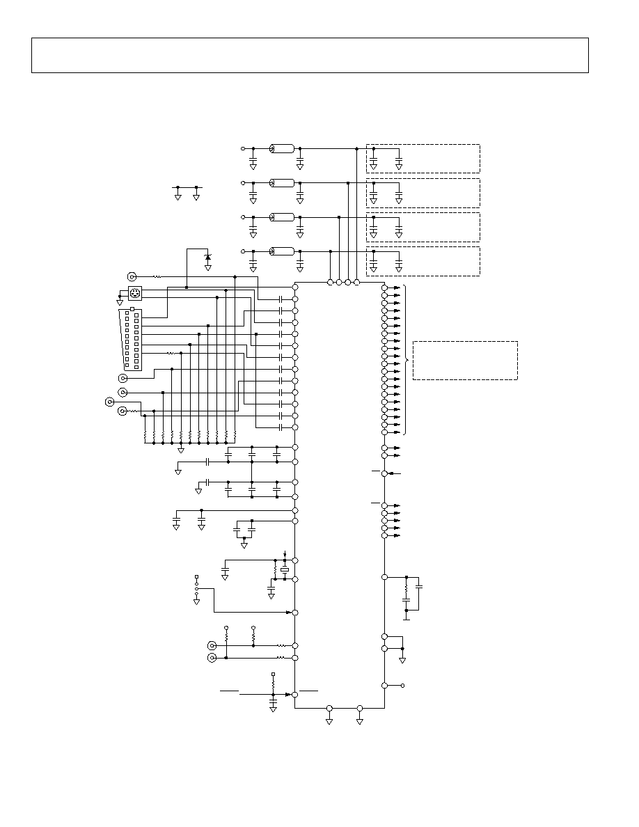
ADV7188
Rev. 0 | Page 108 of 112
TYPICAL CIRCUIT CONNECTION
An example of how to connect the ADV7188 video decoder is shown in Figure 50. For a detailed schematic diagram for the ADV7188,
refer to the ADV7188 evaluation note, which can be obtained from a local ADI representative.
P0
P1
P2
P3
P4
P5
P6
P7
P8
P9
P10
P11
INT
INTERRUPT O/P
P12
SFL
SFL O/P
P13
HS
HS O/P
P14
VS
VS O/P
LLC1
27MHz OUTPUT CLOCK
P15
P16
P17
P18
P19
FIELD
FIELD O/P
LLC2
OE
13.5MHz OUTPUT CLOCK
OUTPUT ENABLE I/P
PVDD
ELPF
10nF
82nF
1.7k
DGND
AGND
DGND
AGND
MULTIFORMAT PIXEL PORT
P19P10 10-BIT
ITU-R BT.656 PIXEL DATA @ 27MHz
P9P0 Cb AND Cr 20-BIT
ITU-R BT.656 PIXEL DATA @ 13.5MHz
P19P10 Y 20-BIT
ITU-R BT.656 PIXEL DATA @ 13.5MHz
0.1
F
DGND
0.01
F
DGND
33
F
DGND
10
F
DGND
FERRITE BEAD
DVDDIO
(3.3V)
POWER SUPPLY
DECOUPLING FOR
EACH POWER PIN
0.1
F
AGND
0.01
F
AGND
33
F
AGND
10
F
AGND
FERRITE BEAD
PVDD
(1.8V)
POWER SUPPLY
DECOUPLING FOR
EACH POWER PIN
0.1
F
AGND
0.01
F
AGND
33
F
AGND
10
F
AGND
FERRITE BEAD
AVDD
(3.3V)
POWER SUPPLY
DECOUPLING FOR
EACH POWER PIN
0.1
F
DGND
0.01
F
DGND
33
F
DGND
10
F
DGND
FERRITE BEAD
DVDD
(1.8V)
POWER SUPPLY
DECOUPLING FOR
EACH POWER PIN
AGND DGND
DVDDI
O
PVDD
AVDD
DVDD
FB
100nF
AIN1
100nF
AIN7
100nF
AIN2
100nF
AIN8
100nF
AIN3
100nF
AIN4
100nF
AIN5
100nF
AIN11
100nF
AIN9
100nF
AIN10
100nF
AIN6
100nF
AIN12
56
75
75
75
75
75
56
75
75
56
75
Pr
Pb
Y
CVBS0
CVBS1
S-VIDEO
Y
C
19
AGND
F_BLNK
BLUE
RED/C
GREEN
CVBS/Y 19
19
AGND
2k
2k
+
CAPY1
CAPY2
AGND
1nF
0.1
F
10
F
0.1
F
+
CAPC1
CAPC2
CML
AGND
1nF
0.1
F
10
F
0.1
F
DGND
DVDDIO
100nF
+
10
F
0.1
F
REFOUT
AGND
0.1
F
10
F
+
XTAL
47pF
1
DGND
XTAL1
ALSB
47pF
1
DGND
DVDDIO
SELECT I
2
C
ADDRESS
DVSS
MPU INTERFACE
CONTROL LINES
SCLK
SDA
100
100
DVDDIO DVDDIO
4.7k
RESET
RESET
05478-053
ADV7188
28.6363MHz
1M
1
LOAD CAP VALUES
ARE DEPENDENT ON
CRYSTAL ATTRIBUTES.
3.3V
TEST6
TEST7
TEST8
AGND
DVDDIO
Figure 50. Typical Connection Diagram
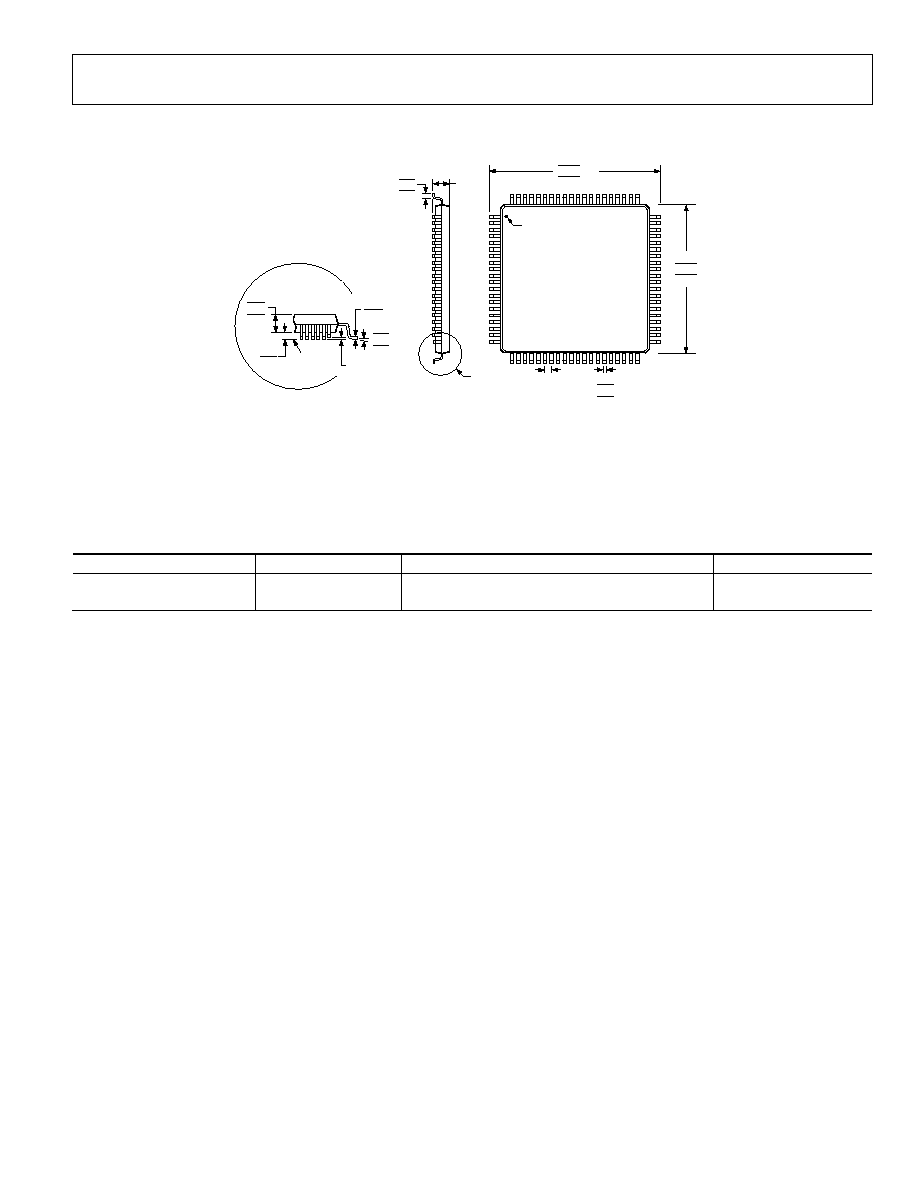
ADV7188
Rev. 0 | Page 109 of 112
OUTLINE DIMENSIONS
COMPLIANT TO JEDEC STANDARDS MS-026-BEC
1.45
1.40
1.35
0.15
0.05
0.20
0.09
0.10 MAX
COPLANARITY
VIEW A
ROTATED 90° CCW
SEATING
PLANE
7°
3.5°
0°
61
60
1
80
20
41
21
40
VIEW A
1.60
MAX
0.75
0.60
0.45
16.20
16.00 SQ
15.80
14.20
14.00 SQ
13.80
0.65
BSC
LEAD PITCH
0.38
0.32
0.22
TOP VIEW
(PINS DOWN)
PIN 1
Figure 51. 80-Lead Low Profile Quad Flat Package [LQFP]
(ST-80-2)
Dimensions shown in millimeters
ORDERING GUIDE
Model
1
Temperature Range
Package Description
Package Option
ADV7188BSTZ
2
40°C to +85°C
80-Lead Low Profile Quad Flat Package (LQFP)
ST-80-2
EVAL-ADV7188EB
Evaluation
Board
1
The ADV7188 is a Pb-free, environmentally friendly product. It is manufactured using the most up-to-date materials and processes. The coating on the leads of each
device is 100% pure Sn electroplate. The device is suitable for Pb-free applications, and is able to withstand surface-mount soldering at up to 255°C (±5°C). In addition,
it is backward-compatible with conventional SnPb soldering processes. This means that the electroplated Sn coating can be soldered with SnPb solder pastes at
conventional reflow temperatures of 220°C to 235°C.
2
Z = Pb-free part.

ADV7188
Rev. 0 | Page 110 of 112
NOTES

ADV7188
Rev. 0 | Page 111 of 112
NOTES

ADV7188
Rev. 0 | Page 112 of 112
NOTES
Purchase of licensed I
2
C components of Analog Devices or one of its sublicensed Associated Companies conveys a license for the purchaser under the Philips I
2
C Patent
Rights to use these components in an I
2
C system, provided that the system conforms to the I
2
C Standard Specification as defined by Philips.
© 2005 Analog Devices, Inc. All rights reserved. Trademarks and
registered trademarks are the property of their respective owners.
D0
547807/05(0)
Document Outline
- þÿ
- þÿ
- þÿ
- þÿ
- þÿ
- þÿ
- þÿ
- þÿ
- þÿ
- þÿ
- þÿ
- þÿ
- þÿ
- þÿ
- þÿ
- þÿ
- þÿ
- þÿ
- þÿ
- þÿ
- þÿ
- þÿ
- þÿ
- þÿ
- þÿ
- þÿ
- þÿ
- þÿ
- þÿ
- þÿ
- þÿ
- þÿ
- þÿ
- þÿ
- þÿ
- þÿ
- þÿ
- þÿ
- þÿ
- þÿ
- þÿ
- þÿ
- þÿ