 | ÐлекÑÑоннÑй компоненÑ: ADV7192K | СкаÑаÑÑ:  PDF PDF  ZIP ZIP |
/home/web/htmldatasheet/RUSSIAN/html/ad/211098
REV. A
Information furnished by Analog Devices is believed to be accurate and
reliable. However, no responsibility is assumed by Analog Devices for its
use, nor for any infringements of patents or other rights of third parties
which may result from its use. No license is granted by implication or
otherwise under any patent or patent rights of Analog Devices.
a
ADV7192
One Technology Way, P.O. Box 9106, Norwood, MA 02062-9106, U.S.A.
Tel: 781/329-4700
World Wide Web Site: http://www.analog.com
Fax: 781/326-8703
© Analog Devices, Inc., 2000
Video Encoder with Six 10-Bit DACs, 54 MHz
Oversampling and Progressive Scan Inputs
FEATURES
Six High-Quality 10-Bit Video DACs
10-Bit Internal Digital Video Processing
Multistandard Video Input
Multistandard Video Output
4 Oversampling with Internal 54 MHz PLL
Programmable Video Control Includes:
Digital Noise Reduction
Gamma Correction
Black Burst
LUMA Delay
CHROMA Delay
Multiple Luma and Chroma Filters
Luma SSAFTM (Super Subalias Filter)
Average Brightness Detection
Field Counter
Macrovision Rev. 7.1
CGMS (Copy Generation Management System)
WSS (Wide Screen Signaling)
Closed Captioning Support.
Teletext Insertion Port (PAL-WST)
2-Wire Serial MPU Interface (I
2
C
®
-Compatible
and Fast I
2
C)
I
2
C Interface
Supply Voltage 5 V and 3.3 V Operation
80-Lead LQFP Package
SSAF is a trademark of Analog Devices Inc.
This device is protected by U.S. patent numbers 4631603, 4577216 and 4819098 and other intellectual property rights.
ITU-R and CCIR are used interchangeably in this document (ITU-R has replaced CCIR recommendations).
I
2
C is a registered trademark of Philips Corporation.
Throughout the document YUV refers to digital or analog component video.
APPLICATIONS
DVD Playback Systems
PC Video/Multimedia Playback Systems
Progressive Scan Playback Systems
GENERAL DESCRIPTION
The ADV7192 is part of the new generation of video encoders
from Analog Devices. The device builds on the performance of
previous video encoders and provides new features like interfac-
ing progressive scan devices, Digital Noise Reduction, Gamma
Correction, 4
×
Oversampling and 54 MHz operation, Average
Brightness Detection, Black Burst Signal Generation, Chroma
Delay, an additional Chroma Filter, and other features.
The ADV7192 supports NTSC-M, NTSC-N (Japan), PAL N,
PAL M, PAL-B/D/G/H/I and PAL-60 standards. Input standards
supported include ITU-R.BT656 4:2:2 YCrCb in 8-bit or 16-bit
format and 3
×
10-Bit YCrCb progressive scan format.
The ADV7192 can output Composite Video (CVBS), S-Video
(Y/C), Component YUV
or RGB and analog progressive scan in
YPrPb format. The analog component output is also compatible
with Betacam, MII, and SMPTE/EBU N10 levels, SMPTE
170 M NTSC, and ITUR.BT 470 PAL.
Please see Detailed Description of Features for more informa-
tion about the ADV7192.
SIMPLIFIED FUNCTIONAL BLOCK DIAGRAM
I
2
C INTERFACE
CHROMA
LPF
10-BIT
DAC
10-BIT
DAC
10-BIT
DAC
10-BIT
DAC
10-BIT
DAC
10-BIT
DAC
2
OVERSAMPLING
4
OVERSAMPLING
OR
ADV7192
SSAF
LPF
LUMA
LPF
COMPOSITE VIDEO
Y [S-VIDEO]
C [S-VIDEO]
RGB
YUV
YPrPb
TV SCREEN
OR
PROGRESSIVE
SCAN DISPLAY
COLOR CONTROL
DNR
GAMMA
CORRECTION
VBI
TELETEXT
CLOSED CAPTION
CGMS/WSS
DEMUX
AND
YCrCb-
TO-
YUV
MATRIX
PLL
AND
54MHz
VIDEO
INPUT
PROCESSING
VIDEO
OUTPUT
PROCESSING
VIDEO
SIGNAL
PROCESSING
ANALOG
OUTPUT
27MHz
CLOCK
ITUR.BT
656/601
8-BIT YCrCb
IN 4:2:2 FORMAT
DIGITAL
INPUT

ADV7192
2
REV. A
CONTENTS
FEATURES . . . . . . . . . . . . . . . . . . . . . . . . . . . . . . . . . . . . . 1
APPLICATIONS . . . . . . . . . . . . . . . . . . . . . . . . . . . . . . . . . 1
GENERAL DESCRIPTION . . . . . . . . . . . . . . . . . . . . . . . . . 1
SIMPLIFIED FUNCTIONAL BLOCK DIAGRAM . . . . . . 1
SPECIFICATIONS
Static Performance 5 V . . . . . . . . . . . . . . . . . . . . . . . . . . . 3
Static Performance 3.3 V . . . . . . . . . . . . . . . . . . . . . . . . . . 4
Dynamic Specifications 5 V . . . . . . . . . . . . . . . . . . . . . . . . 5
Dynamic Specifications 3.3 V . . . . . . . . . . . . . . . . . . . . . . . 5
Timing Characteristics 5 V . . . . . . . . . . . . . . . . . . . . . . . . 6
Timing Characteristics 3.3 V . . . . . . . . . . . . . . . . . . . . . . . 7
ABSOLUTE MAXIMUM RATINGS . . . . . . . . . . . . . . . . . 9
PIN CONFIGURATION . . . . . . . . . . . . . . . . . . . . . . . . . . . 9
ORDERING GUIDE . . . . . . . . . . . . . . . . . . . . . . . . . . . . . . 9
PACKAGE THERMAL PERFORMANCE . . . . . . . . . . . . . 9
PIN FUNCTION DESCRIPTIONS . . . . . . . . . . . . . . . . . 10
DETAILED DESCRIPTION OF FEATURES . . . . . . . . . 11
GENERAL DESCRIPTION . . . . . . . . . . . . . . . . . . . . . . . . 11
DATA PATH DESCRIPTION . . . . . . . . . . . . . . . . . . . . . 12
INTERNAL FILTER RESPONSE . . . . . . . . . . . . . . . . . . . 13
FEATURES: FUNCTIONAL DESCRIPTION . . . . . . . . . 17
BLACK BURST OUTPUT . . . . . . . . . . . . . . . . . . . . . . . . 17
BRIGHTNESS DETECT . . . . . . . . . . . . . . . . . . . . . . . . . . 17
CHROMA/LUMA DELAY . . . . . . . . . . . . . . . . . . . . . . . . 17
CLAMP OUTPUT . . . . . . . . . . . . . . . . . . . . . . . . . . . . . . . 17
CSO, HSO, AND VSO OUTPUTS . . . . . . . . . . . . . . . . . . 17
COLOR BAR GENERATION . . . . . . . . . . . . . . . . . . . . . . 17
COLOR BURST SIGNAL CONTROL . . . . . . . . . . . . . . . 17
COLOR CONTROLS . . . . . . . . . . . . . . . . . . . . . . . . . . . . 17
CHROMINANCE CONTROL . . . . . . . . . . . . . . . . . . . . . 17
UNDERSHOOT LIMITER . . . . . . . . . . . . . . . . . . . . . . . . 18
DIGITAL NOISE REDUCTION . . . . . . . . . . . . . . . . . . . . 18
DOUBLE BUFFERING . . . . . . . . . . . . . . . . . . . . . . . . . . . 18
GAMMA CORRECTION CONTROL . . . . . . . . . . . . . . . 18
NTSC PEDESTAL CONTROL . . . . . . . . . . . . . . . . . . . . . 18
POWER-ON
RESET . . . . . . . . . . . . . . . . . . . . . . . . . . . . . 18
PROGRESSIVE SCAN INPUT . . . . . . . . . . . . . . . . . . . . . 18
REAL-TIME CONTROL, SUBCARRIER RESET, AND
TIMING RESET . . . . . . . . . . . . . . . . . . . . . . . . . . . . . . . 19
SCH PHASE MODE . . . . . . . . . . . . . . . . . . . . . . . . . . . . . 19
SLEEP MODE . . . . . . . . . . . . . . . . . . . . . . . . . . . . . . . . . . 19
SQUARE PIXEL MODE . . . . . . . . . . . . . . . . . . . . . . . . . . 19
VERTICAL BLANKING DATA INSERTION
AND
BLANK INPUT . . . . . . . . . . . . . . . . . . . . . . . . . . . 19
YUV LEVELS . . . . . . . . . . . . . . . . . . . . . . . . . . . . . . . . . . . 20
16-BIT INTERFACE . . . . . . . . . . . . . . . . . . . . . . . . . . . . . 20
4
× OVERSAMPLING AND INTERNAL PLL . . . . . . . . . 20
VIDEO TIMING DESCRIPTION . . . . . . . . . . . . . . . . . . . 20
RESET SEQUENCE . . . . . . . . . . . . . . . . . . . . . . . . . . . . . 20
MPU PORT DESCRIPTION . . . . . . . . . . . . . . . . . . . . . . . 28
REGISTER ACCESSES . . . . . . . . . . . . . . . . . . . . . . . . . . . 29
REGISTER PROGRAMMING . . . . . . . . . . . . . . . . . . . . . 29
MODE REGISTERS 09 . . . . . . . . . . . . . . . . . . . . . . . 3035
TIMING REGISTERS 01 . . . . . . . . . . . . . . . . . . . . . . . . 36
SUBCARRIER FREQUENCY AND
PHASE REGISTERS . . . . . . . . . . . . . . . . . . . . . . . . . . . 37
CLOSED CAPTIONING REGISTERS . . . . . . . . . . . . . . . 37
NTSC PEDESTAL/PAL TELETEXT CONTROL
REGISTERS . . . . . . . . . . . . . . . . . . . . . . . . . . . . . . . . . . 37
TELETEXT REQUEST CONTROL REGISTER . . . . . . 38
CGMS_WSS REGISTERS . . . . . . . . . . . . . . . . . . . . . . . . . 38
CONTRAST CONTROL REGISTER . . . . . . . . . . . . . . . . 39
COLOR CONTROL REGISTERS . . . . . . . . . . . . . . . . . . 39
CC1 AND CC2 BIT DESCRIPTIONS . . . . . . . . . . . . . . . 39
HUE ADJUST CONTROL REGISTER (HCR) . . . . . . . . 40
HCR BIT DESCRIPTION . . . . . . . . . . . . . . . . . . . . . . . . . 40
BRIGHTNESS CONTROL REGISTER (BCR) . . . . . . . . 40
BCR BIT DESCRIPTION . . . . . . . . . . . . . . . . . . . . . . . . . 40
SHARPNESS RESPONSE REGISTER (PR) . . . . . . . . . . . 41
PR BIT DESCRIPTION . . . . . . . . . . . . . . . . . . . . . . . . . . 41
DNR REGISTERS . . . . . . . . . . . . . . . . . . . . . . . . . . . . . . . 41
DNR BIT DESCRIPTIONS . . . . . . . . . . . . . . . . . . . . . . . . 41
GAMMA CORRECTION REGISTERS . . . . . . . . . . . . . . 43
BRIGHTNESS DETECT REGISTER . . . . . . . . . . . . . . . . 44
OUTPUT CLOCK REGISTER . . . . . . . . . . . . . . . . . . . . . 44
OCR BIT DESCRIPTIONS . . . . . . . . . . . . . . . . . . . . . . . . 44
APPENDIX 1
Board Design and Layout Considerations . . . . . . . . . . . . 45
APPENDIX 2
Closed Captioning . . . . . . . . . . . . . . . . . . . . . . . . . . . . . . 47
APPENDIX 3
Copy Generation Management System (CGMS) . . . . . . . 48
APPENDIX 4
Wide Screen Signaling . . . . . . . . . . . . . . . . . . . . . . . . . . . 49
APPENDIX 5
Teletext Insertion . . . . . . . . . . . . . . . . . . . . . . . . . . . . . . . 50
APPENDIX 6
Optional Output Filter . . . . . . . . . . . . . . . . . . . . . . . . . . . 51
APPENDIX 7
DAC Buffering . . . . . . . . . . . . . . . . . . . . . . . . . . . . . . . . . 52
APPENDIX 8
Recommended Register Values . . . . . . . . . . . . . . . . . . . . 53
APPENDIX 9
NTSC Waveforms (With Pedestal) . . . . . . . . . . . . . . . . . 57
NTSC Waveforms (Without Pedestal) . . . . . . . . . . . . . . . 58
PAL Waveforms . . . . . . . . . . . . . . . . . . . . . . . . . . . . . . . . 59
Video Measurement Plots . . . . . . . . . . . . . . . . . . . . . . . . 60
UV Waveforms . . . . . . . . . . . . . . . . . . . . . . . . . . . . . . . . . 64
Output Waveforms . . . . . . . . . . . . . . . . . . . . . . . . . . . . . . 65
APPENDIX 10
Vector Plots . . . . . . . . . . . . . . . . . . . . . . . . . . . . . . . . . . . 68
OUTLINE DIMENSIONS . . . . . . . . . . . . . . . . . . . . . . . . . 69

3
REV. A
ADV7192
5 V SPECIFICATIONS
1
Parameter
Min
Typ
Max
Unit
Test Conditions
STATIC PERFORMANCE
Resolution (Each DAC)
10
Bits
Accuracy (Each DAC)
Integral Nonlinearity
3
1.0
LSB
Differential Nonlinearity
3
1.0
LSB
Guaranteed Monotonic
DIGITAL INPUTS
Input High Voltage, V
INH
2.0
V
Input Low Voltage, V
INL
0.8
V
Input Current, I
IN
0
±1
µA
V
IN
= 0.4 V or 2.4 V
Input Capacitance, C
IN
6
10
pF
Input Leakage Current
4
1
µA
Input Leakage Current
5
200
µA
DIGITAL OUTPUTS
Output High Voltage, V
OH
2.4
V
I
SOURCE
= 400
µA
Output Low Voltage, V
OL
0.8
0.4
V
I
SINK
= 3.2 mA
Three-State Leakage Current
6
10
µA
Three-State Leakage Current
7
200
µA
Three-State Output Capacitance
6
10
pF
ANALOG OUTPUTS
Output Current (Max)
4.125
4.33
4.625
mA
R
L
= 300
Output Current (Min)
2.16
mA
R
L
= 600
R
SET1,
R
SET2
= 2400
DAC-to-DAC Matching
3
0.4
2.5
%
Output Compliance, V
OC
0
1.4
V
Output Impedance, R
OUT
100
k
Output Capacitance, C
OUT
6
pF
I
OUT
= 0 mA
VOLTAGE REFERENCE
Reference Range, V
REF
8
1.112
1.235
1.359
V
POWER REQUIREMENTS
V
AA
4.75
5.0
5.25
V
Normal Power Mode
I
DAC
(Max)
9
29
35
mA
I
CCT
(2
× Oversampling)
10, 11
80
120
mA
I
CCT
(4
× Oversampling)
10, 11
120
170
mA
I
PLL
6
10
mA
Sleep Mode
I
DAC
0.01
µA
I
CCT
85
µA
NOTES
1
All measurements are made in 4
× Oversampling Mode unless otherwise specified.
2
Temperature range T
MIN
to T
MAX
: 0
°C to 70°C.
3
Guaranteed by characterization.
4
For all inputs but PAL_NTSC and ALSB.
5
For PAL_NTSC and ALSB inputs.
6
For all outputs but
VSO/TTX/CLAMP.
7
For
VSO/TTX/CLAMP output.
8
Measurement made in 2
× Oversampling Mode.
9
I
DAC
is the total current required to supply all DACs including the V
REF
Circuitry.
10
All six DACs ON.
11
I
CCT
or the circuit current, is the continuous current required to drive the digital core without I
PLL
.
Specifications subject to change without notice.
(V
AA
= 5 V, V
REF
= 1.235 V, R
SET1,2
= 1200
unless otherwise noted. All specifications T
MIN
to T
MAX
2
unless otherwise noted.)
SPECIFICATIONS

4
REV. A
ADV7192SPECIFICATIONS
3.3 V SPECIFICATIONS
1
Parameter
Min
Typ
Max
Unit
Test Conditions
STATIC PERFORMANCE
Resolution (Each DAC)
10
Bits
Accuracy (Each DAC)
Integral Nonlinearity
1.0
LSB
Differential Nonlinearity
1.0
LSB
Guaranteed Monotonic
DIGITAL INPUTS
Input High Voltage, V
INH
2
V
Input Low Voltage, V
INL
0.8
V
Input Leakage Current
3
1
µA
Input Leakage Current
4
200
µA
Input Current, I
IN
±1
µA
V
IN
= 0.4 V or 2.4 V
Input Capacitance, C
IN
6
10
pF
DIGITAL OUTPUTS
Output High Voltage, V
OH
2.4
V
I
SOURCE
= 400
µA
Output Low Voltage, V
OL
0.4
V
I
SINK
= 3.2 mA
Three-State Leakage Current
5
10
µA
Three-State Leakage Current
6
200
µA
Three-State Output Capacitance
6
10
pF
ANALOG OUTPUTS
Output Current (Max)
4.125
4.33
4.625
mA
R
L
= 300
Output Current (Min)
2.16
mA
R
L
= 600
, R
SET1,2
= 2400
DAC-to-DAC Matching
0.4
2.5
%
Output Compliance, V
OC
1.4
V
Output Impedance, R
OUT
100
k
Output Capacitance, C
OUT
6
pF
I
OUT
= 0 mA
VOLTAGE REFERENCE
Reference Range, V
REF
7
1.235
V
I
VREFOUT
= 20
µA
POWER REQUIREMENTS
V
AA
3.15
3.3
3.6
V
Normal Power Mode
I
DAC
(Max)
8
29
mA
I
CCT
(2
× Oversampling)
9, 10
42
54
mA
I
CCT
(4
× Oversampling)
9, 10
68
86
mA
I
PLL
6
mA
Sleep Mode
I
DAC
10
0.01
µA
I
CCT
85
µA
NOTES
1
All measurements are made in 4
× Oversampling Mode unless otherwise specified and are guaranteed by characterization. In 2 × Oversampling Mode, power require-
ment for the ADV7192 is typically 3.0 V.
2
Temperature range T
MIN
to T
MAX
: 0
°C to 70°C.
3
For all inputs but PAL_NTSC and ALSB.
4
For PAL_NTSC and ALSB inputs.
5
For all outputs but
VSO/TTX/CLAMP.
6
For
VSO/TTX/CLAMP output.
7
Measurement made in 2
× Oversampling Mode.
8
I
DAC
is the total current required to supply all DACs including the V
REF
Circuitry.
9
All six DACs ON.
10
I
CCT
or the circuit current, is the continuous current required to drive the digital core without I
PLL
.
Specifications subject to change without notice.
(V
AA
= 3.3 V,
V
REF
= 1.235 V, R
SET1,2
= 1200 unless otherwise noted. All specifications T
MIN
to T
MAX
2
unless otherwise noted.)

5
REV. A
ADV7192
5 V DYNAMICSPECIFICATIONS
1
Parameter
Min
Typ
Max
Unit
Test Conditions
Hue Accuracy
0.5
Degrees
Color Saturation Accuracy
0.7
%
Chroma Nonlinear Gain
0.7
0.9
±%
Referenced to 40 IRE
Chroma Nonlinear Phase
0.5
±Degrees
Chroma/Luma Intermod
0.1
±%
Chroma/Luma Gain Ineq
1.7
±%
Chroma/Luma Delay Ineq
2.2
ns
Luminance Nonlinearity
0.6
0.7
±%
Chroma AM Noise
82
dB
Chroma PM Noise
72
dB
Differential Gain
3
0.1
(0.4)
0.3 (0.5)
%
Differential Phase
3
0.4
(0.15)
0.5 (0.3)
Degrees
SNR (Pedestal)
3
78.5 (78)
dB rms
RMS
78
(78)
dB p-p
Peak Periodic
SNR (Ramp)
3
61.7 (61.7)
dB rms
RMS
62
(63)
dB p-p
Peak Periodic
NOTES
1
All measurements are made in 4
× Oversampling Mode unless otherwise specified and are guaranteed by characterization.
2
Temperature range T
MIN
to T
MAX
: 0
°C to 70°C.
3
Values in parentheses apply to 2
× Oversampling Mode.
Specifications subject to change without notice.
3.3 V DYNAMICSPECIFICATIONS
1
Parameter
Min
Typ
Max
Unit
Test Conditions
Hue Accuracy
0.5
Degrees
Color Saturation Accuracy
0.8
%
Luminance Nonlinearity
0.6
±%
Chroma AM Noise
83
dB
Chroma PM Noise
71
dB
Chroma Nonlinear Gain
0.7
±%
Referenced to 40 IRE
Chroma Nonlinear Phase
0.5
±Degrees
Chroma/Luma Intermod
0.1
±%
Differential Gain
3
0.2
(0.5)
%
Differential Phase
3
0.5
(0.2)
Degrees
SNR (Pedestal)
3
78.5 (78)
dB rms
RMS
78
(78)
dB p-p
Peak Periodic
SNR (Ramp)
3
62.3 (62)
dB rms
RMS
61
(62.5)
dB p-p
Peak Periodic
NOTES
1
All measurements are made in 4
× Oversampling Mode unless otherwise specified and are guaranteed by characterization.
2
Temperature range T
MIN
to T
MAX
: 0
°C to 70°C.
3
Values in parentheses apply to 2
× Oversampling Mode.
Specifications subject to change without notice.
(V
AA
= 5 V 250 mV, V
REF
= 1.235 V, R
SET1,2
= 1200
unless otherwise noted. All
specifications T
MIN
to T
MAX
2
unless otherwise noted.)
(V
AA
= 3.3 V
150 mV, V
REF
= 1.235 V, R
SET1,2
= 1200
unless otherwise noted. All
specifications T
MIN
to T
MAX
2
unless otherwise noted.)

ADV7192
6
REV. A
5 V TIMING CHARACTERISTICS
Parameter
Min
Typ
Max
Unit
Test Conditions
MPU PORT
2
SCLOCK Frequency
0
400
kHz
SCLOCK High Pulsewidth, t
1
0.6
µs
SCLOCK Low Pulsewidth, t
2
1.3
µs
Hold Time (Start Condition), t
3
0.6
µs
After This Period the First Clock Is Generated
Setup Time (Start Condition), t
4
0.6
µs
Relevant for Repeated Start Condition
Data Setup Time, t
5
100
ns
SDATA, SCLOCK Rise Time, t
6
300
ns
SDATA, SCLOCK Fall Time, t
7
300
ns
Setup Time (Stop Condition), t
8
0.6
µs
ANALOG OUTPUTS
2
Analog Output Delay
8
ns
DAC Analog Output Skew
0.1
ns
CLOCK CONTROL AND PIXEL
PORT
3
f
CLOCK
27
MHz
Clock High Time, t
9
8
2
ns
Clock Low Time, t
10
8
3
ns
Data Setup Time, t
11
6
2.5
ns
Data Hold Time, t
12
5
2.0
ns
Control Setup Time, t
11
6
ns
Control Hold Time, t
12
4
ns
Digital Output Access Time, t
13
13
ns
Digital Output Hold Time, t
14
12
ns
Pipeline Delay, t
15
(2
× Oversampling)
57
Clock Cycles
Pipeline Delay, t
15
(4
× Oversampling)
67
Clock Cycles
TELETEXT PORT
4
Digital Output Access Time, t
16
11
ns
Data Setup Time, t
17
3
ns
Data Hold Time, t
18
6
ns
RESET CONTROL
RESET Low Time
3
20
ns
PLL
2
PLL Output Frequency
54
MHz
NOTES
1
Temperature range T
MIN
to T
MAX
: 0
°C to 70°C.
2
Guaranteed by characterization.
3
Pixel Port consists of:
Data: P7P0, Y0/P8Y7/P15 Pixel Inputs
Control:
HSYNC, VSYNC, BLANK
Clock: CLKIN
4
Teletext Port consists of:
Digital Output: TTXREQ
Data: TTX
Specifications subject to change without notice.
(V
AA
= 5 V 250 mV, V
REF
= 1.235 V, R
SET1,2
= 1200 V unless otherwise noted. All
specifications T
MIN
to T
MAX
1
unless otherwise noted.)

ADV7192
7
REV. A
3.3 V TIMING CHARACTERISTICS
Parameter
Min
Typ
Max
Unit
Test Conditions
MPU PORT
SCLOCK Frequency
0
400
kHz
SCLOCK High Pulsewidth, t
1
0.6
µs
SCLOCK Low Pulsewidth, t
2
1.3
µs
Hold Time (Start Condition), t
3
0.6
µs
After This Period the First Clock Is Generated
Setup Time (Start Condition), t
4
0.6
µs
Relevant for Repeated Start Condition
Data Setup Time, t
5
100
ns
SDATA, SCLOCK Rise Time, t
6
300
ns
SDATA, SCLOCK Fall Time, t
7
300
ns
Setup Time (Stop Condition), t
8
0.6
2
µs
ANALOG OUTPUTS
Analog Output Delay
8
ns
DAC Analog Output Skew
0.1
ns
CLOCK CONTROL AND PIXEL
PORT
3
f
CLOCK
27
MHz
Clock High Time, t
9
8
2
ns
Clock Low Time, t
10
8
3
ns
Data Setup Time, t
11
6
4
ns
Data Hold Time, t
12
4
2.0
ns
Control Setup Time, t
11
2, 5
ns
Control Hold Time, t
12
3
ns
Digital Output Access Time, t
13
13
ns
Digital Output Hold Time, t
14
12
ns
Pipeline Delay, t
15
(2
× Oversampling)
37
Clock Cycles
TELETEXT PORT
4
Digital Output Access Time, t
16
11
ns
Data Setup Time, t
17
3
ns
Data Hold Time, t
18
6
ns
RESET CONTROL
RESET Low Time
3
20
ns
PLL
PLL Output Frequency
54
MHz
NOTES
1
Temperature range T
MIN
to T
MAX
: 0
°C to 70°C.
2
Guaranteed by characterization.
3
Pixel Port consists of:
Data: P7P0, Y0/P8Y7/P15 Pixel Inputs
Control:
HSYNC, VSYNC, BLANK
Clock: CLKIN
4
Teletext Port consists of:
Digital Output: TTXREQ
Data: TTX
Specifications subject to change without notice.
(V
AA
= 3.3 V 150 mV, V
REF
= 1.235 V, R
SET1,2
= 1200
unless otherwise noted. All
specifications T
MIN
to T
MAX
1
unless otherwise noted.)
2
ADV7192
8
REV. A
t
3
t
2
t
6
t
1
t
7
t
5
t
3
t
4
t
8
SDA
SCL
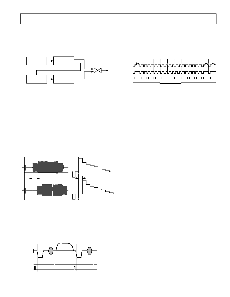
Figure 1. MPU Port Timing Diagram
t
9
t
11
CLOCK
PIXEL INPUT
DATA
t
10
t
12
HSYNC,
VSYNC,
BLANK
Cb
Y
Cr
Y
Cb
Y
HSYNC,
VSYNC,
BLANK,
CSO_HSO,
VSO, CLAMP
t
13
t
14
CONTROL
I/PS
CONTROL
O/PS
Figure 2. Pixel and Control Data Timing Diagram
t
16
t
17
t
18
TTXREQ
CLOCK
TTX
4 CLOCK
CYCLES
4 CLOCK
CYCLES
4 CLOCK
CYCLES
3 CLOCK
CYCLES
4 CLOCK
CYCLES
Figure 3. Teletext Timing Diagram
t
9
t
10
t
12
Y0
Y1
Y2
Y3
Y4
Y5
Cb0
Cb1
Cb2
Cb3
Cb4
Cb5
Cr0
Cr1
Cr2
Cr3
Cr4
Cr5
t
11
CLOCK
Y0Y9
INCLUDING
SYNC
INFORMATION
Cb0Cb9
Cr0Cr9
PROGRESSIVE
SCAN INPUT
Figure 4. Progressive Scan Input Timing
ADV7192
9
REV. A
ABSOLUTE MAXIMUM RATINGS
1
V
AA
to GND . . . . . . . . . . . . . . . . . . . . . . . . . . . . . . . . . . . 7 V
Voltage on any Digital Input Pin . . GND 0.5 V to V
AA
+ 0.5 V
Storage Temperature (T
S
) . . . . . . . . . . . . . . 65
°C to +150°C
Junction Temperature (T
J
) . . . . . . . . . . . . . . . . . . . . . . 150
°C
Body Temperature (Soldering, 10 secs) . . . . . . . . . . . . . 220
°C
Analog Outputs to GND
2
. . . . . . . . . . . . GND 0.5 V to V
AA
NOTES
1
Stresses above those listed under Absolute Maximum Ratings may cause perma-
nent damage to the device. This is a stress rating only; functional operation of the
device at these or any other conditions above those listed in the operational sections
of this specification is not implied. Exposure to absolute maximum rating condi-
tions for extended periods may affect device reliability.
2
Analog Output Short Circuit to any Power Supply or Common can be of an
indefinite duration.
PACKAGE THERMAL PERFORMANCE
The 80-lead package is used for this device. The junction-to-
ambient (
JA
) thermal resistance in still air on a four-layer PCB
is 24.7
°C.
To reduce power consumption when using this part the user
can run the part on a 3.3 V supply, turn off any unused DACs.
The user must at all times stay below the maximum junction
temperature of 110
°C. The following equation shows how to
calculate this junction temperature:
Junction Temperature = (V
AA
× (I
DAC
+ I
CCT
))
×
JA
+ 70
°C T
AMB
I
DAC
= 10 mA + (sum of the average currents consumed by
each powered-on DAC)
Average current consumed by each powered-on DAC =
(V
REF
× K )/R
SET
V
REF
= 1.235 V
K = 4.2146
ORDERING GUIDE
Model
Temperature Range
Package Description
Package Option
ADV7192KST
0
°C to 70°C
80-Lead Quad Flatpack
ST-80
CAUTION
ESD (electrostatic discharge) sensitive device. Electrostatic charges as high as 4000 V readily
accumulate on the human body and test equipment and can discharge without detection. Although
the ADV7192 features proprietary ESD protection circuitry, permanent damage may occur on
devices subjected to high-energy electrostatic discharges. Therefore, proper ESD precautions are
recommended to avoid performance degradation or loss of functionality.
WARNING!
ESD SENSITIVE DEVICE
PIN CONFIGURATION
NC = NO CONNECT
P0
P1
P2
P3
P4
P5
P6
P7
NC
NC
Y[0]/P8
Y[1]/P9
Y[2]/P10
Y[3]/P11
Y[4]/P12
Y[5]/P13
Y[6]/P14
Y[7]/P15
Y[8]
Y[9]
V
REF
COMP 1
DAC A
DAC B
V
AA
AGND
DAC C
DAC D
AGND
V
AA
DAC E
DAC F
COMP 2
R
SET2
DGND
RESET
PAL_NTSC
R
SET1
ALSB
SCRESET/RTC/TR
DGND
HSYNC
VSYNC
BLANK
TTXREQ
DGND
V
DD
AGND
V
AA
SCL
SDA
CLKIN
CLKOUT
V
DD
Cb[4]
Cb[5]
Cb[6]
Cb[7]
Cb[8]
Cb[9]
80 79 78 77 76
71 70 69 68 67 66 65
75 74 73 72
64 63 62 61
1
2
3
4
5
6
7
8
9
10
11
13
14
15
16
12
17
18
20
19
21 22 23 24 25 26 27 28 29 30 31 32 33 34 35 36 37 38 39 40
PIN 1
IDENTIFIER
TOP VIEW
(Not to Scale)
60
59
58
57
56
55
54
53
52
51
50
49
48
47
46
45
44
43
42
41
DGND
V
DD
Cb[3]
DGND
VSO
/
TTX
/
CLAMP
CSO_HSO
Cb[2]
Cb[1]
Cb[0]
Cr[9]
Cr[8]
Cr[7]
Cr[6]
Cr[5]
V
DD
Cr[4]
Cr[3]
Cr[2]
Cr[1]
Cr[0]
ADV7192
LQFP

ADV7192
10
REV. A
PIN FUNCTION DESCRIPTIONS
Pin
Input/
No.
Mnemonic
Output
Function
1, 2
NC
No Connect.
310
P0P7
I
8-Bit 4:2:2 Multiplexed YCrCb Pixel Port. The LSB of the input data is set up on Pin P0
(Pin Number 3).
1118
Y0/P8Y7/P15
I
16-Bit 4:2:2 Multiplexed YCrCb Pixel Port (Bits 815). 1
× 10-Bit Progressive Scan Input for
Ydata (Bits 07).
19, 20
Y8Y9
1
× 10-Bit Progressive Scan Input Is Ydata (Bits 8 and 9).
21, 34, 68, 79
V
DD
P
Digital Power Supply (3.3 V to 5 V).
22, 33, 43, 69,
DGND
G
Digital Ground.
80
23
HSYNC
I/O
HSYNC (Modes 1, 2, and 3) Control Signal. This pin may be configured to be an output
(Master Mode) or an input (Slave Mode) and accept Sync Signals.
24
VSYNC
I/O
VSYNC Control Signal. This pin may be configured as an output (Master Mode) or as an
input (Slave Mode) and accept
VSYNC as a Control Signal.
25
BLANK
I/O
Video Blanking Control Signal. This signal is optional. For further information see
Vertical Blanking and Data Insertion Blanking Input section.
2631, 7578
Cb4Cb9, Cb0Cb3
I
1
× 10-Bit Progressive Scan Input Port for Cb Data.
32
TTXREQ
O
Teletext Data Request Output Signal, used to control teletext data transfer.
35, 49, 52
AGND
G
Analog Ground.
36
CLKIN
I
TTL Clock Input. Requires a stable 27 MHz reference clock for standard operation.
Alternatively, a 24.5454 MHz (NTSC) or 29.5 MHz (PAL) can be used for square pixel
operation.
37
CLKOUT
O
Clock Output Pin.
38, 48, 53
V
AA
P
Analog Power Supply (3.3 V to 5 V).
39
SCL
I
MPU Port Serial Interface Clock Input.
40
SDA
I/O
MPU Port Serial Data Input/Output.
41
SCRESET/
I
Multifunctional Input: Real Time Control (RTC) input, Timing Reset input, Subcarrier
RTC/TR
Reset input.
42
ALSB
I
TTL Address Input. This signal sets up the LSB of the MPU address.
44
R
SET2
I
A 1200
resistor connected from this pin to AGND is used to control full-scale amplitudes
of the Video Signals from the DAC D, E, F.
45
COMP 2
O
Compensation Pin for DACs D, E, and F. Connect a 0.1
µF Capacitor from COMP2
to V
AA
.
46
DAC F
O
S-Video C/Pr/V/RED Analog Output. This DAC is capable of providing 4.33 mA output.
47
DAC E
O
S-Video Y/Pb/U/BLUE Analog Output. This DAC is capable of providing 4.33 mA output.
50
DAC D
O
Composite/Y (Progressive Scan)/Y/Green Analog Output. This DAC is capable of providing
4.33 mA output.
51
DAC C
O
S-Video C/Pr/V/RED Analog Output. This DAC is capable of providing 4.33 mA output.
54
DAC B
O
S-Video Y/Pb/U/BLUE Analog Output. This DAC is capable of providing 4.33 mA output.
55
DAC A
O
Composite/Y(Progressive Scan)/Y/Green Analog Output. This DAC is capable of providing
4.33 mA output.
56
COMP 1
O
Compensation Pin for DACs A, B, and C. Connect a 0.1
µF Capacitor from COMP1 to V
AA
.
57
V
REF
I/O
Voltage Reference Input for DACs or Voltage Reference Output (1.235 V). An external
V
REF
cannot be used in 4
× Oversampling Mode.
58
R
SET1
I
A 1200
resistor connected from this pin to AGND is used to control full-scale amplitudes
of the Video Signals from the DAC A, B, C.
59
PAL_NTSC
I
Input signal to select PAL or NTSC mode of operation, pin set to Logic 1 selects PAL.
60
RESET
I
The input resets the on-chip timing generator and sets the ADV7192 into default mode.
See Appendix 8 for Default Register settings.
61
CSO_HSO
O
Dual function
CSO or HSO Output Sync Signal at TTL Level.
62
VSO/TTX/CLAMP
I/O
Multifunctional Pin.
VSO Output Sync Signal at TTL level. Teletext Data Input pin.
CLAMP TTL output signals can be used to drive external circuitry to enable clamping
of all video signals.
6367, 7074
Cr0Cr4, Cr5Cr9
I
1
× 10-Bit Progressive Scan Input Port for Cr Data.
ADV7192
11
REV. A
DETAILED DESCRIPTION OF FEATURES
Clocking:
Single 27 MHz Clock Required to Run the Device
4 Oversampling with Internal 54 MHz PLL
Square Pixel Operation
Advanced Power Management
Programmable Video Control Features:
Digital Noise Reduction
Black Burst Signal Generation
Pedestal Level
Hue, Brightness, Contrast, and Saturation
Clamping Output Signal
VBI (Vertical Blanking Interval)
Subcarrier Frequency and Phase
LUMA Delay
CHROMA Delay
Gamma Correction
Luma And Chroma Filters
Luma SSAF (Super Subalias Filter)
Average Brightness Detection
Field Counter
Interlaced/Noninterlaced Operation
Complete On-Chip Video Timing Generator
Programmable Multimode Master/Slave Operation
Macrovision Rev 7.1
CGMS (Copy Generation Management System)
WSS (Wide Screen Signaling)
Closed Captioning Support
Teletext Insertion Port (PAL-WST)
2-Wire Serial MPU Interface
(I
2
C-Compatible and Fast I
2
C)
I
2
C Registers Synchronized to VSYNC
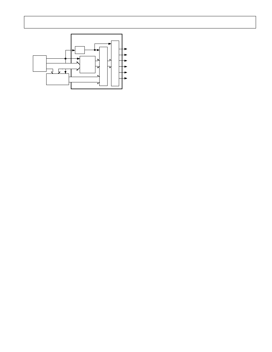
GENERAL DESCRIPTION
The ADV7192 is an integrated Digital Video Encoder that
converts digital CCIR-601/656 4:2:2 8-bit or 16-bit component
video data into a standard analog baseband television signal
compatible with worldwide standards. Additionally, it is possible
I
N
T
E
R
P
O
L
A
T
O
R
MODULATOR
AND
HUE CONTROL
BRIGHTNESS
CONTROL
AND
ADD SYNC
AND
INTERPOLATOR
SATURATION
CONTROL
AND
ADD BURST
AND
INTERPOLATOR
PROGRAMMABLE
LUMA FILTER
AND
SHARPNESS
FILTER
PROGRAMMABLE
CHROMA
FILTER
SIN/COS
DDS
BLOCK
REAL-TIME
CONTROL
CIRCUIT
SCRESET/RTC/TR
I
N
T
E
R
P
O
L
A
T
O
R
M
U
L
T
I
P
L
E
X
E
R
YUV-TO-RGB
MATRIX
AND
YUV LEVEL
CONTROL
BLOCK
Y0Y9
Cb0Cb9
Cr0Cr9
10-BIT
DAC
10-BIT
DAC
10-BIT
DAC
DAC
CONTROL
BLOCK
10-BIT
DAC
10-BIT
DAC
10-BIT
DAC
DAC
CONTROL
BLOCK
DAC A
DAC B
DAC C
V
REF
R
SET2
COMP2
DAC D
DAC F
DAC E
R
SET1
COMP1
DNR
AND
GAMMA
CORRECTION
10
10
10
V
U
Y
YCrCb-
TO-
YUV
MATRIX
10
10
10
V
U
Y
PLL
DEMUX
10 10
10
TELETEXT
INSERTION
BLOCK
VIDEO TIMING
GENERATOR
CGMS/WSS
AND
CLOSED CAPTIONING
CONTROL
I
2
C MPU PORT
ALSB
SDA
SCL
PAL_NTSC
VSO/CLAMP
CSO_HSO
HSYNC
VSYNC
BLANK
RESET
TTX
TTXREQ
P0
P15
CLKIN
CLKOUT
ADV7192
Figure 5. Detailed Functional Block Diagram
to input video data in 3 10-bit YCrCb progressive scan format
to facilitate interfacing devices such as progressive scan systems.
Six DACs are available on the ADV7192, each of which is capable
of providing 4.33 mA of current. In addition to the composite
output signal there is the facility to output S-Video (Y/C Video),
RGB Video and YUV Video. All YUV formats (SMPTE/EBU
N10, MII or Betacam) are supported.
The on-board SSAF (Super Subalias Filter) with extended lumi-
nance frequency response and sharp stopband attenuation
enables studio quality video playback on modern TVs, giving
optimal horizontal line resolution. An additional sharpness
control feature allows high-frequency enhancement on the
luminance signal.
SUBTRACT SIGNAL IN THRESHOLD
RANGE FROM ORIGINAL SIGNAL
FILTER OUTPUT
>THRESHOLD?
FILTER OUTPUT<
THRESHOLD
INPUT FILTER
BLOCK
MAIN SIGNAL PATH
NOISE SIGNAL PATH
Y DATA
INPUT
DNR OUT
ADD SIGNAL ABOVE THRESHOLD
RANGE TO ORIGINAL SIGNAL
DNR CONTROL
BLOCK SIZE CONTROL
BORDER AREA
BLOCK OFFSET
GAIN
CORING GAIN DATA
CORING GAIN BORDER
DNR SHARPNESS MODE
FILTER OUTPUT
<THRESHOLD?
FILTER OUTPUT>
THRESHOLD
INPUT FILTER
BLOCK
MAIN SIGNAL PATH
NOISE SIGNAL PATH
Y DATA
INPUT
DNR OUT
DNR CONTROL
BLOCK SIZE CONTROL
BORDER AREA
BLOCK OFFSET
GAIN
CORING GAIN DATA
CORING GAIN BORDER
DNR MODE
Figure 6. Block Diagram for DNR Mode and DNR Sharpness
Mode
ADV7192
12
REV. A
Digital Noise Reduction allows improved picture quality in remov-
ing low amplitude, high frequency noise. Figure 6 shows the DNR
functionality in the two modes available.
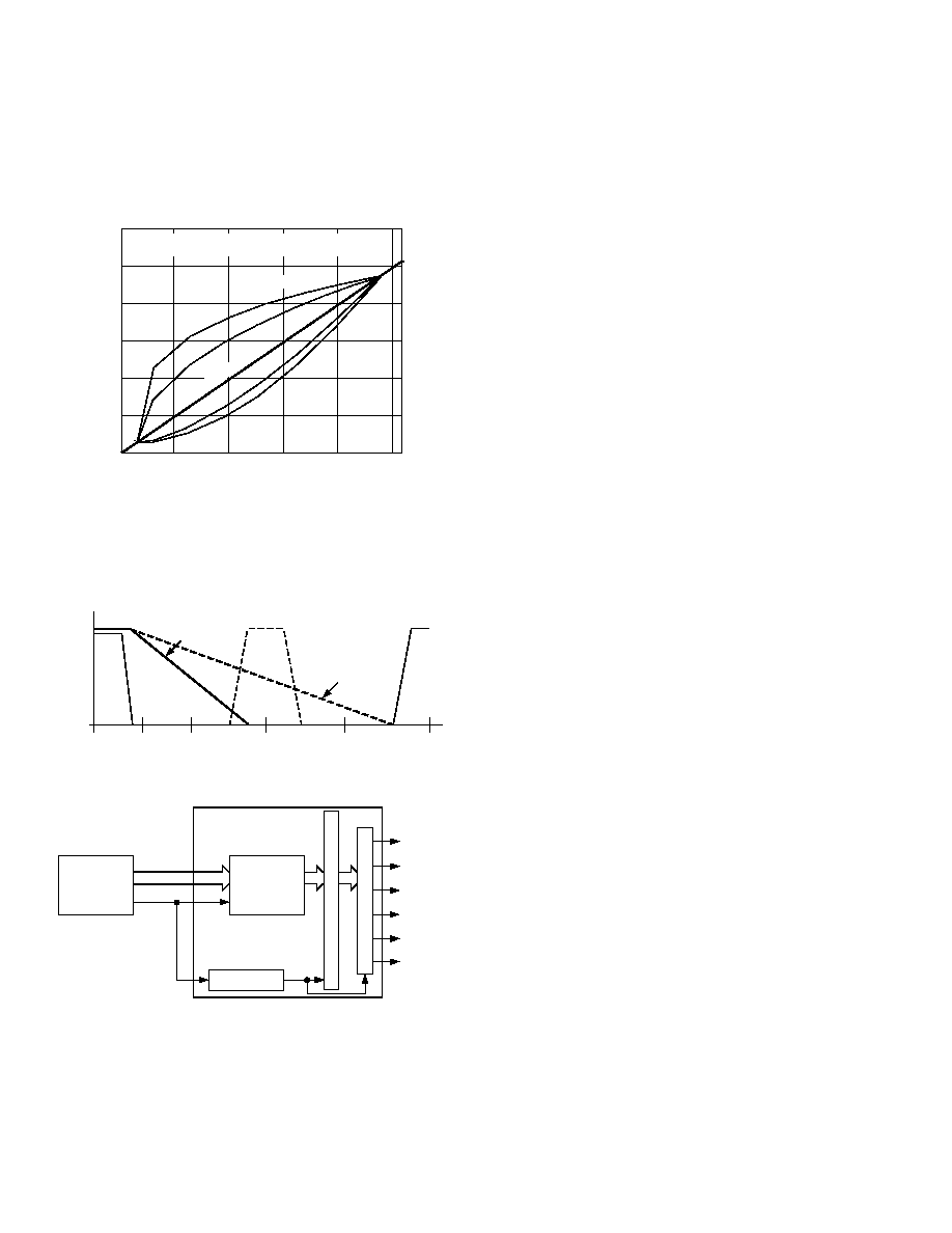
Programmable gamma correction is also available. The figure below
shows the response of different gamma values to a ramp signal.
250
200
150
100
50
0
300
SIGNAL OUTPUTS
SIGNAL INPUT
0.5
GAMMA CORRECTION BLOCK OUTPUT
TO A RAMP INPUT FOR VARIOUS GAMMA VALUES
GAMMA-CORRECTED AMPLITUDE
0
50
100
150
200
250
LOCATION
0.3
1.5
1.8
Figure 7. Signal Input (Ramp) and Selectable Gamma
Output Curves
The device is driven by a 27 MHz clock. Data can be output at
27 MHz or 54 MHz (on-board PLL) when 4 oversampling is
enabled. Also, the output filter requirements in 4 oversampling
and 2 oversampling differ, as can be seen in Figure 8.
30dB
0dB
6.75MHz
13.5MHz
27.0MHz
40.5MHz
54.0MHz
2 FILTER
REQUIREMENTS
4 FILTER
REQUIREMENTS
Figure 8. Output Filter Requirements in 4
× Oversampling
Mode
ENCODER
CORE
2
I
N
T
E
R
P
O
L
A
T
I
O
N
6
D
A
C
O
U
T
P
U
T
S
54MHz
OUTPUT
RATE
ADV7192
PLL
54MHz
MPEG2
PIXEL BUS
27MHz
Figure 9. PLL and 4
× Oversampling Block Diagram
The ADV7192 also supports both PAL and NTSC square pixel
operation. In this case the encoder requires a 24.5454 MHz Clock
for NTSC or 29.5 MHz Clock for PAL square pixel mode opera-
tion. All internal timing is generated on-chip.
An advanced power management circuit enables optimal control
of power consumption in normal operating modes or sleep modes.
The Output Video Frames are synchronized with the incoming
data Timing Reference Codes. Optionally, the Encoder accepts
(and can generate)
HSYNC, VSYNC, and FIELD timing signals.
These timing signals can be adjusted to change pulsewidth and
position while the part is in master mode.
HSO/CSO and VSO TTL outputs are also available and are timed
to the analog output video.
A separate teletext port enables the user to directly input teletext
data during the vertical blanking interval.
The ADV7192 also incorporates WSS and CGMS-A data control
generation.
The ADV7192 modes are set up over a 2-wire serial bidirectional
port (I
2
C-compatible) with two slave addresses, and the device
is register-compatible with the ADV7172.
The ADV7192 is packaged in an 80-lead LQFP package.
DATA PATH DESCRIPTION
For PAL B, D, G, H, I, M, N, and NTSCM, N modes, YCrCb
4:2:2 data is input via the CCIR-656/601-compatible Pixel Port
at a 27 MHz Data Rate. The Pixel Data is demultiplexed to form
three data paths. Y typically has a range of 16 to 235, Cr and Cb
typically have a range of 128 112; however, it is possible to
input data from 1 to 254 on both Y, Cb, and Cr. The ADV7192
supports PAL (B, D, G, H, I, N, M) and NTSCM, N (with
and without Pedestal) and PAL60 standards.
Digital noise reduction can be applied to the Y signal. Pro-
grammable gamma correction can also be applied to the Y
signal if required.
The Y data can be manipulated for contrast control and a setup
level can be added for brightness control. The Cr, Cb data can
be scaled to achieve color saturation control. All settings become
effective at the start of the next field when double buffering is
enabled.
The appropriate sync, blank, and burst levels are added to the
YCrCb data. Macrovision antitaping, closed-captioning and
teletext levels are also added to Y and the resultant data is inter-
polated to 54 MHz (4 Oversampling Mode). The interpolated
data is filtered and scaled by three digital FIR filters.
The U and V signals are modulated by the appropriate Subcarrier
Sine/Cosine waveforms and a phase offset may be added onto
the color subcarrier during active video to allow hue adjustment.
The resulting U and V signals are added together to make up
the Chrominance signal. The Luma (Y) signal can be delayed
by up to six clock cycles (at 27 MHz) and the Chroma signal
can be delayed by up to eight clock cycles (at 27 MHz).
The Luma and Chroma signals are added together to make up
the Composite Video Signal. All timing signals are controlled.
The YCrCb data is also used to generate RGB data with appropri-
ate sync and blank levels. The YUV levels are scaled to output
the suitable SMPTE/EBU N10, MII, or Betacam levels.
Each DAC can be individually powered off if not required. A
complete description of DAC output configurations is given in
the Mode Register 2 section.
Video output levels are illustrated in Appendix 9.
ADV7192
13
REV. A
Table I. Luminance Internal Filter Specifications (4 Oversampling)
Passband
3 dB Bandwidth
2
Filter Type
Filter Selection
Ripple
1
(dB)
(MHz)
MR04 MR03 MR02
Low-Pass (NTSC)
0
0
0
0.16
4.24
Low-Pass (PAL)
0
0
1
0.1
4.81
Notch (NTSC)
0
1
0
0.09
2.3/4.9/6.6
Notch (PAL)
0
1
1
0.1
3.1/5.6/6.4
Extended (SSAF)
1
0
0
0.04
6.45
CIF
1
0
1
0.127
3.02
QCIF
1
1
0
Monotonic
1.5
NOTES
1
Passband Ripple is defined as the fluctuations from the 0 dB response in the passband, measured in (dB). The
passband is defined to have 0fc frequency limits for a low-pass filter, 0f1 and f2infinity for a notch filter,
where fc, f1, f2 are the 3 dB points.
2
3 dB bandwidth refers to the 3 dB cutoff frequency.
Table II. Chrominance Internal Filter Specifications (4 Oversampling)
Passband
3 dB Bandwidth
2
Filter Type
Filter Selection
Ripple
1
(dB)
(MHz)
MR07 MR06 MR05
1.3 MHz Low-Pass
0
0
0
0.09
1.395
0.65 MHz Low-Pass
0
0
1
Monotonic
0.65
1.0 MHz Low-Pass
0
1
0
Monotonic
1.0
2.0 MHz Low-Pass
0
1
1
0.048
2.2
3.0 MHz Low-Pass
1
1
1
Monotonic
3.2
CIF
1
0
1
Monotonic
0.65
QCIF
1
1
0
Monotonic
0.5
NOTES
1
Passband Ripple is defined as the fluctuations from the 0 dB response in the passband, measured in (dB). The
passband is defined to have 0fc frequency limits for a low-pass filter, 0f1 and f2infinity for a notch filter,
where fc, f1, f2 are the 3 dB points.
2
3 dB bandwidth refers to the 3 dB cutoff frequency.
When to used to interface progressive scan systems, the ADV7192
allows to input YCrCb signals in Progressive Scan format
(3
10-bit) before these signals are routed to the interpolation
filters and the DACs.
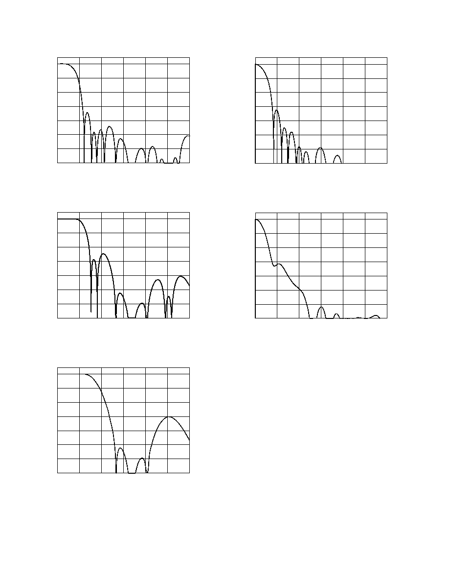
INTERNAL FILTER RESPONSE
The Y Filter supports several different frequency responses
including two low-pass responses, two notch responses, an
Extended (SSAF) response with or without gain boost/attenuation,
a CIF response, and a QCIF response. The UV filters support
several different frequency responses including five low-pass
responses, a CIF response, and a QCIF response, as can be seen in
the following figures. All filter plots show the 4 Oversampling
responses.
In Extended Mode there is the option of 12 responses in the range
from 4 dB to +4 dB. The desired response can be chosen by the
user by programming the correct value via the I
2
C. The variation
of frequency responses can be seen in the Tables I and II. For
more detailed filter plots refer to Analog Devices' Application
Note AN-562.
0
20
0
50
60
30
10
2
4
10
12
6
8
70
40
FREQUENCY MHz
MAGNITUDE
dB
TPC 1. NTSC Low-Pass Luma Filter
0
20
0
50
60
30
10
2
4
10
12
6
8
70
40
FREQUENCY MHz
MAGNITUDE
dB
TPC 2. PAL Low-Pass Luma Filter
0
20
0
50
60
30
10
2
4
10
12
6
8
70
40
MAGNITUDE
dB
FREQUENCY MHz
TPC 3. NTSC Notch Luma Filter
0
20
0
50
60
30
10
2
4
10
12
6
8
70
40
MAGNITUDE
dB
FREQUENCY MHz
TPC 4. PAL Notch Luma Filter
0
20
0
50
60
30
10
2
4
10
12
6
8
70
40
MAGNITUDE
dB
FREQUENCY MHz
TPC 5. Extended Mode (SSAF) Luma Filter
4
0
0
8
6
2
2
1
2
6
7
3
5
12
4
MAGNITUDE
dB
FREQUENCY MHz
10
4
TPC 6. Extended SSAF Luma Filter and Programmable
Gain/Attenuation Showing +4 dB/12 dB Range
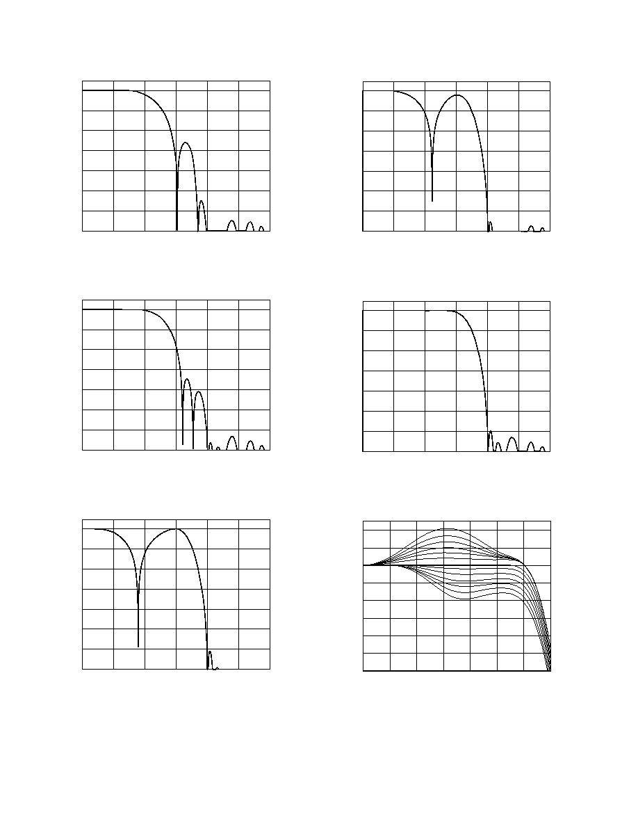
ADV7192Typical Performance Characteristics
14
REV. A
ADV7192
15
REV. A
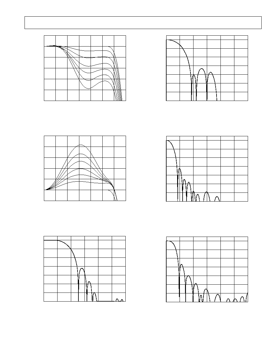
1
0
4
3
1
0
1
2
6
7
3
5
5
2
MAGNITUDE
dB
FREQUENCY MHz
4
TPC 7. Extended SSAF and Programmable Attenuation,
Showing Range 0 dB/4 dB
5
0
0
1
3
4
1
2
6
7
3
5
1
2
MAGNITUDE
dB
FREQUENCY MHz
4
TPC 8. Extended SSAF and Programmable Gain, Showing
Range 0 dB/+4 dB
0
20
0
50
60
30
10
2
4
10
12
6
8
70
40
MAGNITUDE
dB
FREQUENCY MHz
TPC 9. Luma CIF Filter
0
20
0
50
60
30
10
2
4
10
12
6
8
70
40
MAGNITUDE
dB
FREQUENCY MHz
TPC 10. Luma QCIF Filter
0
20
0
50
60
30
10
2
4
10
12
6
8
70
40
MAGNITUDE
dB
FREQUENCY MHz
TPC 11. Chroma 0.65 MHz Low-Pass Filter
0
20
0
50
60
30
10
2
4
10
12
6
8
70
40
MAGNITUDE
dB
FREQUENCY MHz
TPC 12. Chroma 1.0 MHz Low-Pass Filter
ADV7192
16
REV. A
0
20
0
50
60
30
10
2
4
10
12
6
8
70
40
MAGNITUDE
dB
FREQUENCY MHz
TPC 13. Chroma 1.3 MHz Low-Pass Filter
0
20
0
50
60
30
10
2
4
10
12
6
8
70
40
MAGNITUDE
dB
FREQUENCY MHz
TPC 14. Chroma 2 MHz Low-Pass Filter
0
20
0
50
60
30
10
2
4
10
12
6
8
70
40
MAGNITUDE
dB
FREQUENCY MHz
TPC 15. Chroma 3 MHz Low-Pass Filter
0
20
0
50
60
30
10
2
4
10
12
6
8
70
40
MAGNITUDE
dB
FREQUENCY MHz
TPC 16. Chroma CIF Filter
0
20
0
50
60
30
10
2
4
10
12
6
8
70
40
MAGNITUDE
dB
FREQUENCY MHz
TPC 17. Chroma QCIF Filter
ADV7192
17
REV. A
FEATURES: FUNCTIONAL DESCRIPTION
BLACK BURST OUTPUT
It is possible to output a black burst signal from two DACs. This
signal output is very useful for professional video equipment
since it enables two video sources to be locked together. (Mode
Register 9.)
BLACK BURST OUTPUT
CVBS
CVBS
DIGITAL DATA
GENERATOR
ADV7192
DIGITAL DATA
GENERATOR
ADV7192
Figure 10. Possible Application for the Black Burst Output
Signal
BRIGHTNESS DETECT
This feature is used to monitor the average brightness of the
incoming Y video signal on a field by field basis. The information
is read from the I
2
C and based on this information the color
saturation, contrast and brightness controls can be adjusted (for
example to compensate for very dark pictures). (Brightness Detect
Register.)
CHROMA/LUMA DELAY
The luminance data can be delayed by maximum of six clock
cycles. Additionally the Chroma can be delayed by a maximum
of eight clock cycles (one clock cycle at 27 MHz). (Timing Reg-
ister 0 and Mode Register 9.)
CHROMA DELAY
LUMA DELAY
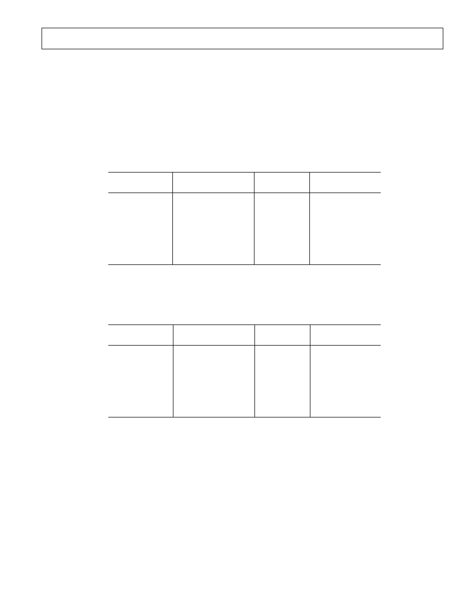
Figure 11. Chroma Delay Figure 12. Luma Delay
CLAMP OUTPUT
The ADV7192 has a programmable clamp TTL output signal.
This clamp signal is programmable to the front and back porch.
The clamp signal can be varied by one to three clock cycles in a
positive and negative direction from the default position.
(Mode Register 5, Mode Register 7.)
CVBS
OUTPUT PIN
CLAMP
OUTPUT PIN
MR57 = 1
MR57 = 0
CLAMP O/P SIGNALS
Figure 13. Clamp Output Timing
CSO, HSO, AND VSO OUTPUTS
The ADV7192 supports three output timing signals,
CSO
(composite sync signal),
HSO (Horizontal Sync Signal) and
VSO (Vertical Sync Signal). These output TTL signals are aligned
with the analog video outputs. See Figure 14 for an example
of these waveforms. (Mode Register 7.)
OUTPUT
VIDEO
525
1
2
3
4
5
6
7
8
9
10
1119
EXAMPLE:- NTSC
CSO
HSO
VSO
Figure 14.
CSO, HSO, VSO Timing Diagram
COLOR BAR GENERATION
The ADV7192 can be configured to generate 100/7.5/75/7.5
color bars for NTSC or 100/0/75/0 color bars for PAL. (Mode
Register 4.)
COLOR BURST SIGNAL CONTROL
The burst information can be switched on and off the composite
and chroma video output. (Mode Register 4.)
COLOR CONTROLS
The ADV7192 allows the user to control the brightness, contrast,
hue and saturation of the color. The control registers may be
double-buffered, meaning that any modification to the registers
will be done outside the active video region and, therefore, changes
made will not be visible during active video.
Contrast Control
Contrast adjustment is achieved by scaling the Y input data by a
factor programmed by the user. This factor allows the data to be
scaled between 0% and 150%. (Contrast Control Register.)
Brightness Control
The brightness is controlled by adding a programmable setup level
onto the scaled Y data. This brightness level may be added onto
the Y data. For NTSC with pedestal, the setup can vary from
0 IRE to 22.5 IRE. For NTSC without pedestal and PAL, the
setup can vary from 7.5 IRE to +15 IRE. (Brightness Control
Register.)
Color Saturation
Color adjustment is achieved by scaling the Cr and Cb input
data by a factor programmed by the user. This factor allows the
data to be scaled between 0% and 200%. (U Scale Register and
V Scale Register.)
Hue Adjust Control
The hue adjustment is achieved on the composite and chroma
outputs by adding a phase offset onto the color subcarrier in the
active video but leaving the color burst unmodified, i.e., only
the phase between the video and the colorburst is modified and
hence the hue is shifted. The ADV7192 provides a range of
± 22° in increments of 0.17578125°. (Hue Adjust Register.)
CHROMINANCE CONTROL
The color information can be switched on and off the com-
posite, chroma and color component video outputs. (Mode
Register 4.)
ADV7192
18
REV. A
UNDERSHOOT LIMITER
A limiter is placed after the digital filters. This prevents any
synchronization problems for TVs. The level of undershoot is
programmable between 1.5 IRE, 6 IRE, 11 IRE when oper-
ating in 4
× Oversampling Mode. In 2× Oversampling Mode the
limits are 7.5 IRE and 0 IRE. (Mode Register 9 and Timing
Register 0.)
DIGITAL NOISE REDUCTION
DNR is applied to the Y data only. A filter block selects the
high frequency, low amplitude components of the incoming
signal (DNR Input Select). The absolute value of the filter output
is compared to a programmable threshold value (DNR Thresh-
old Control). There are two DNR modes available: DNR Mode
and DNR Sharpness Mode.
In DNR Mode, if the absolute value of the filter output is smaller
than the threshold, it is assumed to be noise. A programmable
amount (Coring Gain Control) of this noise signal will be sub-
tracted from the original signal.
In DNR Sharpness Mode, if the absolute value of the filter output
is less than the programmed threshold, it is assumed to be noise,
as before. Otherwise, if the level exceeds the threshold, now
being identified as a valid signal, a fraction of the signal (Coring
Gain Control) will be added to the original signal in order to boost
high frequency components and to sharpen the video image.
In MPEG systems it is common to process the video information
in blocks of 8
× 8 pixels for MPEG2 systems, or 16 × 16 pixels
for MPEG1 systems ('Block Size Control'). DNR can be applied
to the resulting block transition areas that are known to contain
noise. Generally the block transition area contains two pixels. It
is possible to define this area to contain four pixels (Border Area
Control).
It is also possible to compensate for variable block positioning or
differences in YCrCb pixel timing with the use of the Block Offset
Control. (Mode Register 8, DNR Registers 02.)
DOUBLE BUFFERING
Double buffering can be enabled or disabled on the following
registers: Closed Captioning Registers, Brightness Control Reg-
ister, V-Scale, U-Scale Contrast Control Register, Hue Adjust
Register, Macrovision Registers, and the Gamma Curve Select
bit. These registers are updated once per field on the falling
edge of the
VSYNC signal. Double Buffering improves the overall
performance of the ADV7192, since modifications to register
settings will not be made during active video, but take effect on
the start of the active video. (Mode Register 8.)
GAMMA CORRECTION CONTROL
Gamma correction may be performed on the luma data. The
user has the choice to use either of two different gamma curves,
A or B. At any one time one of these curves is operational if
gamma correction is enabled. Gamma correction allows the
mapping of the luma data to a user-defined function. (Mode
Register 8, Gamma Correction Registers 013.)
NTSC PEDESTAL CONTROL
In NTSC mode it is possible to have the pedestal signal gener-
ated on the output video signal. (Mode Register 2.)
POWER-ON
RESET
After power-up, it is necessary to execute a
RESET operation. A
reset occurs on the falling edge of a high-to-low transition on the
RESET pin. This initializes the pixel port such that the data on
the pixel inputs pins is ignored. See Appendix 8 for the register
settings after
RESET is applied.
PROGRESSIVE SCAN INPUT
It is possible to input data to the ADV7192 in progressive scan
format. For this purpose the input pins Y0/P8Y7/P15, Y8Y9,
Cr0Cr9 and Cb0Cb9 accept 10-bit Y data, 10-bit Cb data
and 10-bit Cr data. The data is clocked into the part at 27 MHz.
The data is then filtered and sinc corrected in an 2 Interpo-
lation filter and then output to three video DACs at 54 MHz
(to interface to a progressive scan monitor).
FREQUENCY MHz
0
0
30
5
AMPLITUDE
dB
10
15
20
25
10
20
30
50
60
40
70
Figure 15. Plot of the Interpolation Filter for the Y Data
FREQUENCY MHz
0
0
30
5
AMPLITUDE
dB
10
15
20
25
10
20
30
50
60
40
70
Figure 16. Plot of the Interpolation Filter for the CrCb Data
It is assumed that there is no color space conversion or any other
such operation to be performed on the incoming data. Thus if
these DAC outputs are to drive a TV, all relevant timing and
synchronization data should be contained in the incoming digital
Y data. An FPGA can be used to achieve this,
The block diagram below shows a possible configuration for
progressive scan mode using the ADV7192.
ADV7192
19
REV. A
27MHz
54MHz
6
D
A
C
O
U
T
P
U
T
S
ENCODER
ADV7192
MPEG2
PLL
ENCODER
CORE
PIXEL BUS
I
N
T
E
R
P
O
L
A
T
I
O
N
2
PROGRESSIVE
SCAN
DECODER
30-BIT INTERFACE
Figure 17. Block Diagram Using the ADV7192 in Progres-
sive Scan Mode
The progressive scan decoder deinterlaces the data from the
MPEG2 decoder. This now means that there are 525 video lines
per field in NTSC mode and 625 video lines per field in PAL
mode. The duration of the video line is now 32
µs.
It is important to note that the data from the MPEG2 decoder
is in 4:2:2 format. The data output from the progressive scan
decoder is in 4:4:4 format. Thus it is assumed that some form of
interpolation on the color component data is performed in the
progressive scan decoder IC. (Mode Register 8.)
REAL-TIME CONTROL, SUBCARRIER RESET, AND
TIMING RESET
Together with the SCRESET/RTC/TR pin and Mode Register 4
(Genlock Control), the ADV7192 can be used in (a) Timing
Reset Mode, (b) Subcarrier Phase Reset Mode or (c) RTC Mode.
(a) A TIMING RESET is achieved in holding this pin high. In
this state the horizontal and vertical counters will remain reset.
On releasing this pin (set to low), the internal counters will
commence counting again. The minimum time the pin has
to be held high is 37 ns (1 clock cycle at 27 MHz), otherwise
the reset signal might not be recognized.
(b) The SUBCARRIER PHASE will reset to that of Field 0 at
the start of the following field when a low to high transition
occurs on this input pin.
(c) In RTC MODE, the ADV7192 can be used to lock to an
external video source.
The real-time control mode allows the ADV7192 to auto-
matically alter the subcarrier frequency to compensate for line
length variations. When the part is connected to a device
that outputs a digital datastream in the RTC format (such as
a ADV7185 video decoder, see Figure 21), the part will
automatically change to the compensated subcarrier frequency
on a line-by-line basis. This digital datastream is 67 bits
wide and the subcarrier is contained in Bits 0 to 21. Each bit
is two clock cycles long. 00Hex should be written into all four
Subcarrier Frequency registers when using this mode. (Mode
Register 4.)
SCH PHASE MODE
The SCH phase is configured in default mode to reset every
four (NTSC) or eight (PAL) fields to avoid an accumulation of
SCH phase error over time. In an ideal system, zero SCH phase
error would be maintained forever, but in reality, this is impos-
sible to achieve due to clock frequency variations. This effect is
reduced by the use of a 32-bit DDS, which generates this SCH.
Resetting the SCH phase every four or eight fields avoids the
accumulation of SCH phase error, and results in very minor SCH
phase jumps at the start of the four or eight field sequence.
Resetting the SCH phase should not be done if the video source
does not have stable timing or the ADV7192 is configured in RTC
mode. Under these conditions (unstable video) the Subcarrier
Phase Reset should be enabled but no reset applied. In this
configuration the SCH Phase will never be reset; this means that
the output video will now track the unstable input video. The Sub-
carrier Phase Reset when applied will reset the SCH phase to Field
0 at the start of the next field (e.g., Subcarrier Phase Reset applied
in Field 5 (PAL) on the start of the next field SCH phase will be
reset to Field 0). (Mode Register 4.)
SLEEP MODE
If, after
RESET, the SCRESET/RTC/TR and NTSC_PAL pins
are both set high, the ADV7192 will power up in Sleep Mode to
facilitate low power consumption before all registers have been
initialized.
If Power-up in Sleep Mode is disabled, Sleep Mode control
passes to the Sleep Mode control in Mode Register 2 (i.e., con-
trol via I
2
C). (Mode Register 2 and Mode Register 6.)
SQUARE PIXEL MODE
The ADV7192 can be used to operate in square pixel mode. For
NTSC operation an input clock of 24.5454 MHz is required.
Alternatively, for PAL operation, an input clock of 29.5 MHz
is required. The internal timing logic adjusts accordingly for
square pixel mode operation. Square pixel mode is not available
in 4
× Oversampling mode. (Mode Register 2.)
VERTICAL BLANKING DATA INSERTION AND
BLANK
INPUT
It is possible to allow encoding of incoming YCbCr data on
those lines of VBI that do not have line sync or pre-/post-equal-
ization pulses . This mode of operation is called Partial Blanking. It
allows the insertion of any VBI data (Opened VBI) into the
encoded output waveform, this data is present in digitized
incoming YCbCr data stream (e.g., WSS data, CGMS, VPS
etc.). Alternatively the entire VBI may be blanked (no VBI data
inserted) on these lines. VBI is available in all timing modes.
It is possible to allow control over the
BLANK signal using
Timing Register 0. When the
BLANK input is enabled (TR03 =
0 and input pin tied low), the
BLANK input can be used to
input externally generated blank signals in Slave Mode 1, 2, or
3. When the
BLANK input is disabled (TR03 = 1 and input pin
tied low or tied high) the
BLANK input is not used and the
ADV7192 automatically blanks all normally blank lines as per
CCIR-624. (Timing Register 0.)
ADV7192
20
REV. A
YUV LEVELS
This functionality allows the ADV7192 to output SMPTE levels
or Betacam levels on the Y output when configured in PAL or
NTSC mode.
Sync
Video
Betacam
286 mV
714 mV
SMPTE
300 mV
700 mV
MII
300 mV
700 mV
As the data path is branched at the output of the filters, the luma
signal relating to the CVBS or S-Video Y/C output is unaltered.
Only the Y output of the YCrCb outputs is scaled. This control
allows color component levels to have a peak-peak amplitude of
700 mV, 1000 mV or the default values of 934 mV in NTSC and
700 mV in PAL. (Mode Register 5.)
16-BIT INTERFACE
It is possible to input data in 16-bit format. In this case, the
interface only operates if the data is accompanied by separate
HSYNC/VSYNC/BLANK signals. Sixteen-bit mode is not
available in Slave Mode 0 since EAV/SAV timing codes are
used. (Mode Register 8.)
4 OVERSAMPLING AND INTERNAL PLL
It is possible to operate all six DACs at 27 MHz (2
× Oversam-
pling) or 54 MHz (4
× Oversampling).
The ADV7192 is supplied with a 27 MHz clock synced with the
incoming data. Two options are available: to run the device
throughout at 27 MHz or to enable the PLL. In the latter case,
even if the incoming data runs at 27 MHz, 4
× Oversampling and
the internal PLL will output the data at 54 MHz.
NOTE
In 4
× Oversampling Mode the requirements for the optional
output filters are different from those in 2
× Oversampling. (Mode
Register 1, Mode Register 6.) See Appendix 6.
ENCODER
CORE
2
I
N
T
E
R
P
O
L
A
T
I
O
N
6
D
A
C
O
U
T
P
U
T
S
54MHz
OUTPUT
ENCODE
ADV7192
PLL
54MHz
MPEG2
PIXEL BUS
27MHz
Figure 18. PLL and 4
× Oversampling Block Diagram
30dB
0dB
6.75MHz
13.5MHz
27.0MHz
40.5MHz
54.0MHz
2 FILTER
REQUIREMENTS
4 FILTER
REQUIREMENTS
Figure 19. Output Filter Requirements in 2
× and 4× Over-
sampling Mode
VIDEO TIMING DESCRIPTION
The ADV7192 is intended to interface to off-the-shelf MPEG1
and MPEG2 Decoders. As a consequence, the ADV7192 accepts
4:2:2 YCrCb Pixel Data via a CCIR-656 Pixel Port and has
several Video Timing Modes of operation that allow it to be
configured as either System Master Video Timing Generator or
a Slave to the System Video Timing Generator. The ADV7192
generates all of the required horizontal and vertical timing periods
and levels for the analog video outputs.
The ADV7192 calculates the width and placement of analog
sync pulses, blanking levels, and color burst envelopes. Color
bursts are disabled on appropriate lines and serration and equal-
ization pulses are inserted where required.
In addition the ADV7192 supports a PAL or NTSC square pixel
operation. The part requires an input pixel clock of 24.5454 MHz
for NTSC square pixel operation and an input pixel clock of
29.5 MHz for PAL square pixel operation. The internal horizontal
line counters place the various video waveform sections in the cor-
rect location for the new clock frequencies.
The ADV7192 has four distinct Master and four distinct Slave
timing configurations. Timing Control is established with
the bidirectional
HSYNC, BLANK and VSYNC pins. Tim-
ing Register 1 can also be used to vary the timing pulsewidths
and where they occur in relation to each other. (Mode Regis-
ter 2, Timing Register 0, 1.)
RESET SEQUENCE
When
RESET becomes active the ADV7192 reverts to the default
output configuration (see Appendix 8 for register settings). The
ADV7192 internal timing is under the control of the logic level
on the NTSC_PAL pin.
When
RESET is released Y, Cr, Cb values corresponding to a
black screen are input to the ADV7192. Output timing signals
are still suppressed at this stage. DACs A, B, C are switched off
and DACs D, E, F are switched on.
When the user requires valid data, Pixel Data Valid Control is
enabled (MR26 = 1) to allow the valid pixel data to pass through
the encoder. Digital output timing signals become active and the
encoder timing is now under the control of the Timing Regis-
ters. If at this stage, the user wishes to select a different video
standard to that on the NTSC_PAL pin, Standard I
2
C Control
should be enabled (MR25 = 1) and the video standard required
is selected by programming Mode Register 0 (Output Video Stan-
dard Selection). Figure 20 illustrates the
RESET sequence timing.
ADV7192
21
REV. A
XXXXXXX
XXXXXXX
XXXXXXX
XXXXXXX
XXXXXXX
XXXXXXX
XXXXXXX
OFF
0
DIGITAL TIMING SIGNALS SUPPRESSED
TIMING ACTIVE
1
VALID VIDEO
VALID VIDEO
VALID VIDEO
BLACK VALUE
BLACK VALUE WITH SYNC
RESET
DAC D,
DAC E
DAC F
DAC A,
DAC B,
DAC C
MR26
PIXEL_DATA_VALID
DIGITAL TIMING
Figure 20.
RESET Sequence Timing Diagram
COMPOSITE
VIDEO
e.g., VCR
OR CABLE
CLOCK
GREEN/COMPOSITE/Y
BLUE/LUMA/U
ADV7192
P7P0
SCRESET/RTC/TR
VIDEO
DECODER
ADV7185
LCC1
P19P12
RED/CHROMA/V
GREEN/COMPOSITE/Y
BLUE/LUMA/U
RED/CHROMA/V
H/L TRANSITION
COUNT START
LOW
128
RTC
TIME SLOT: 01
14
67 68
NOT USED IN
ADV7192
19
VALID
SAMPLE
INVALID
SAMPLE
F
SC
PLL INCREMENT
1
8/LINE
LOCKED CLOCK
5 BITS
RESERVED
SEQUENCE
BIT
2
RESET
BIT
3
RESERVED
4 BITS
RESERVED
21
0
13
14 BITS
RESERVED
0
NOTES:
1
F
SC
PLL INCREMENT IS 22 BITS LONG, VALUE LOADED INTO ADV7192 FSC DDS REGISTER IS F
SC
PLL INCREMENTS
BITS 21:0 PLUS BITS 0:9 OF SUBCARRIER FREQUENCY REGISTERS. ALL ZEROS SHOULD BE WRITTEN TO THE
SUBCARRIER FREQUENCY REGISTERS OF THE ADV7192.
2
SEQUENCE BIT
PAL: 0 = LINE NORMAL, 1 = LINE INVERTED
NTSC: 0 = NO CHANGE
3
RESET BIT
RESET ADV7192's DDS
GLL
Figure 21. RTC Timing and Connections
ADV7192
22
REV. A
Mode 0 (CCIR656): Slave Option
(Timing Register 0 TR0 = X X X X X 0 0 0)
The ADV7192 is controlled by the SAV (Start Active Video) and EAV (End Active Video) Time Codes in the Pixel Data. All timing
information is transmitted using a 4-byte Synchronization Pattern. A synchronization pattern is sent immediately before and after each line
during active picture and retrace. Mode 0 is illustrated in Figure 22. The
HSYNC, VSYNC and BLANK (if not used) pins should be
tied high during this mode. Blank output is available.
Y
C
r Y
F
F
0
0
0
0
X
Y
8
0
1
0
8
0
1
0
F
F
0
0
F
F
A
B
A
B
A
B
8
0
1
0
8
0
1
0
F
F
0
0
0
0
X
Y
C
b Y
C
r
C
b
Y
C
b
Y
C
r
EAV CODE
SAV CODE
ANCILLARY DATA
(HANC)
4 CLOCK
4 CLOCK
268 CLOCK
1440 CLOCK
4 CLOCK
4 CLOCK
280 CLOCK
1440 CLOCK
END OF ACTIVE
VIDEO LINE
START OF ACTIVE
VIDEO LINE
ANALOG
VIDEO
INPUT PIXELS
NTSC/PAL M SYSTEM
(525 LlNES/60Hz)
PAL SYSTEM
(625 LINES/50Hz)
Y
Figure 22. Timing Mode 0, Slave Mode
Mode 0 (CCIR656): Master Option
(Timing Register 0 TR0 = X X X X X 0 0 1)
The ADV7192 generates H, V, and F signals required for the SAV (Start Active Video) and EAV (End Active Video) Time Codes in the
CCIR656 standard. The H bit is output on the
HSYNC pin, the V bit is output on the BLANK pin and the F bit is output on the
VSYNC pin. Mode 0 is illustrated in Figure 23 (NTSC) and Figure 24 (PAL). The H, V, and F transitions relative to the video waveform
are illustrated in Figure 25.
522
523
524
525
1
2
3
4
5
6
7
8
9
10
11
20
21
22
DISPLAY
DISPLAY
VERTICAL BLANK
ODD FIELD
EVEN FIELD
H
V
F
260
261
262
263
264
265
266
267
268
269
270
271
272
273
274
283
284
285
ODD FIELD
EVEN FIELD
DISPLAY
DISPLAY
VERTICAL BLANK
H
V
F
Figure 23. Timing Mode 0, NTSC Master Mode
ADV7192
23
REV. A
622
623
624
625
1
2
3
4
5
6
7
21
22
23
DISPLAY
DISPLAY
VERTICAL BLANK
H
V
F
ODD FIELD
EVEN FIELD
309
310
311
312
314
315
316
317
318
319
320
334
335
336
313
DISPLAY
DISPLAY
VERTICAL BLANK
H
V
F
ODD FIELD
EVEN FIELD
Figure 24. Timing Mode 0, PAL Master Mode
ANALOG
VIDEO
H
F
V
Figure 25. Timing Mode 0 Data Transitions, Master Mode
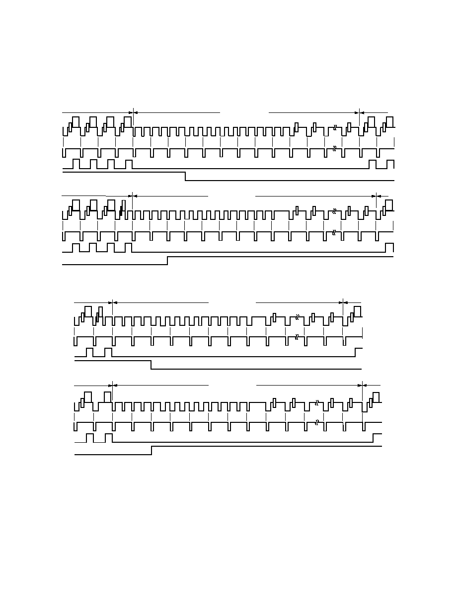
ADV7192
24
REV. A
Mode 1: Slave Option
HSYNC, BLANK, FIELD
(Timing Register 0 TR0 = X X X X X 0 1 0)
In this mode the ADV7192 accepts Horizontal SYNC and Odd/ Even FIELD signals. A transition of the FIELD input when
HSYNC
is low indicates a new frame, i.e., Vertical Retrace. The
BLANK signal is optional. When the BLANK input is disabled the ADV7192
automatically blanks all normally blank lines as per CCIR-624. Mode 1 is illustrated in Figure 26 (NTSC) and Figure 27 (PAL).
260
261
262
263
264
265
266
267
268
269
270
271
272
273
274
283
284
285
ODD FIELD
EVEN FIELD
DISPLAY
DISPLAY
VERTICAL BLANK
HSYNC
BLANK
FIELD
522
523
524
525
1
2
3
4
5
6
7
8
9
10
11
20
21
22
DISPLAY
DISPLAY
VERTICAL BLANK
ODD FIELD
EVEN FIELD
HSYNC
BLANK
FIELD
Figure 26. Timing Mode 1, NTSC
622
623
624
625
1
2
3
4
5
6
7
21
22
23
DISPLAY
VERTICAL BLANK
ODD FIELD
EVEN FIELD
HSYNC
BLANK
FIELD
DISPLAY
309
310
311
312
313
314
315
316
317
318
319
334
335
336
320
DISPLAY
VERTICAL BLANK
ODD FIELD
EVEN FIELD
HSYNC
BLANK
FIELD
DISPLAY
Figure 27. Timing Mode 1, PAL
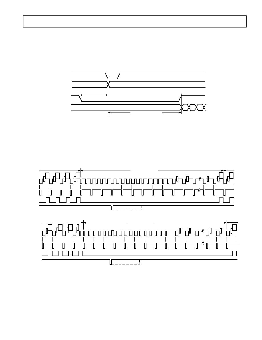
ADV7192
25
REV. A
Mode 1: Master Option
HSYNC, BLANK, FIELD
(Timing Register 0 TR0 = X X X X X 0 1 1)
In this mode the ADV7192 can generate Horizontal SYNC and Odd/Even FIELD signals. A transition of the FIELD input when
HSYNC is low indicates a new frame i.e., Vertical Retrace. The BLANK signal is optional. When the BLANK input is disabled the
ADV7192 automatically blanks all normally blank lines as per CCIR-624. Pixel data is latched on the rising clock edge following the
timing signal transitions. Mode 1 is illustrated in Figure 26 (NTSC) and Figure 27 (PAL). Figure 28 illustrates the
HSYNC, BLANK and
FIELD for an odd or even field transition relative to the pixel data.
FIELD
PIXEL
DATA
PAL = 12 CLOCK/2
NTSC = 16 CLOCK/2
Cb
Y
Cr
Y
HSYNC
BLANK
PAL = 132 CLOCK/2
NTSC = 122 CLOCK/2
Figure 28. Timing Mode 1 Odd/Even Field Transitions Master/Slave
Mode 2: Slave Option
HSYNC, VSYNC, BLANK
(Timing Register 0 TR0 = X X X X X 1 0 0)
In this mode the ADV7192 accepts Horizontal and Vertical SYNC signals. A coincident low transition of both
HSYNC and VSYNC
inputs indicates the start of an Odd Field. A
VSYNC low transition when HSYNC is high indicates the start of an Even Field.
The
BLANK signal is optional. When the BLANK input is disabled the ADV7192 automatically blanks all normally blank lines
as per CCIR-624. Mode 2 is illustrated in Figure 29 (NTSC) and Figure 30 (PAL).
522
523
524
525
1
2
3
4
5
6
7
8
9
10
11
20
21
22
DISPLAY
DISPLAY
VERTICAL BLANK
ODD FIELD
EVEN FIELD
HSYNC
BLANK
VSYNC
260
261
262
263
264
265
266
267
268
269
270
271
272
273
274
283
284
285
ODD FIELD
EVEN FIELD
DISPLAY
DISPLAY
VERTICAL BLANK
HSYNC
BLANK
VSYNC
Figure 29. Timing Mode 2, NTSC
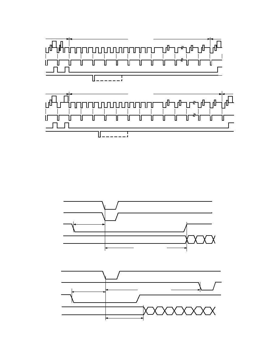
ADV7192
26
REV. A
622
623
624
625
1
2
3
4
5
6
7
21
22
23
DISPLAY
VERTICAL BLANK
ODD FIELD
EVEN FIELD
HSYNC
BLANK
VSYNC
DISPLAY
309
310
311
312
313
314
315
316
317
318
319
334
335
336
320
DISPLAY
VERTICAL BLANK
ODD FIELD
EVEN FIELD
HSYNC
BLANK
DISPLAY
VSYNC
Figure 30. Timing Mode 2, PAL
Mode 2: Master Option
HSYNC, VSYNC, BLANK
(Timing Register 0 TR0 = X X X X X 1 0 1)
In this mode the ADV7192 can generate Horizontal and Vertical SYNC signals. A coincident low transition of both
HSYNC and
VSYNC inputs indicates the start of an Odd Field. A VSYNC low transition when HSYNC is high indicates the start of an Even
Field. The
BLANK signal is optional. When the BLANK input is disabled the ADV7192 automatically blanks all normally blank lines as
per CCIR-624. Mode 2 is illustrated in Figure 29 (NTSC) and Figure 30 (PAL). Figure 31 illustrates the
HSYNC, BLANK and
VSYNC for an even-to-odd field transition relative to the pixel data. Figure 32 illustrates the HSYNC, BLANK and VSYNC for
an odd-to-even field transition relative to the pixel data.
PAL = 12 CLOCK/2
NTSC = 16 CLOCK/2
HSYNC
VSYNC
BLANK
PIXEL
DATA
PAL = 132 CLOCK/2
NTSC = 122 CLOCK/2
Cb
Y
Cr
Y
Figure 31. Timing Mode 2, Even-to-Odd Field Transition Master/Slave
PAL = 864 CLOCK/2
NTSC = 858 CLOCK/2
PAL = 132 CLOCK/2
NTSC = 122 CLOCK/2
HSYNC
VSYNC
BLANK
PIXEL
DATA
PAL = 12 CLOCK/2
NTSC = 16 CLOCK/2
Cb
Y
Cr
Y
Cb
Figure 32. Timing Mode 2, Odd-to-Even Field Transition Master/Slave
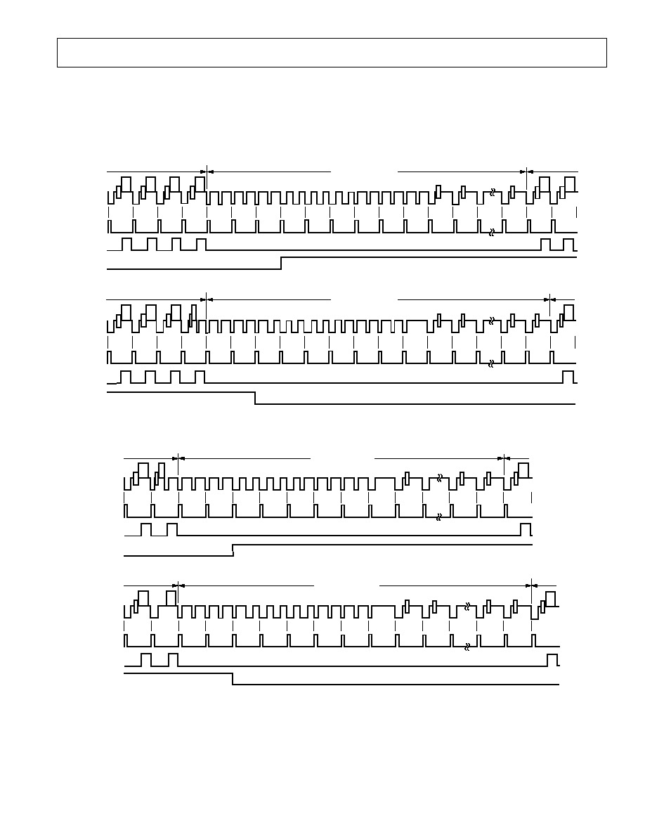
ADV7192
27
REV. A
Mode 3: Master/Slave Option HSYNC, BLANK, FIELD
(Timing Register 0 TR0 = X X X X X 1 1 0 or X X X X X 1 1 1)
In this mode the ADV7192 accepts or generates Horizontal SYNC and Odd/Even FIELD signals. A transition of the FIELD input when
HSYNC is high indicates a new frame i.e., Vertical Retrace. The BLANK signal is optional. When the BLANK input is disabled the
ADV7192 automatically blanks all normally blank lines as per CCIR-624. Mode 3 is illustrated in Figure 33 (NTSC) and
Figure 34 (PAL).
260
261
262
263
264
265
266
267
268
269
270
271
272
273
274
283
284
285
ODD FIELD
EVEN FIELD
DISPLAY
DISPLAY
VERTICAL BLANK
HSYNC
BLANK
FIELD
522
523
524
525
1
2
3
4
5
6
7
8
9
10
11
20
21
22
DISPLAY
DISPLAY
VERTICAL BLANK
ODD FIELD
EVEN FIELD
HSYNC
BLANK
FIELD
Figure 33. Timing Mode 3, NTSC
622
623
624
625
1
2
3
4
5
6
7
21
22
23
DISPLAY
VERTICAL BLANK
ODD FIELD
EVEN FIELD
HSYNC
BLANK
FIELD
DISPLAY
309
310
311
312
313
314
315
316
317
318
319
334
335
336
320
DISPLAY
VERTICAL BLANK
ODD FIELD
EVEN FIELD
HSYNC
BLANK
FIELD
DISPLAY
Figure 34. Timing Mode 3, PAL
ADV7192
28
REV. A
MPU PORT DESCRIPTION
The ADV7192 support a two-wire serial (I
2
C-compatible)
microprocessor bus driving multiple peripherals. Two inputs,
Serial Data (SDA) and Serial Clock (SCL), carry information
between any device connected to the bus. Each slave device is
recognized by a unique address. The ADV7192 has four possible
slave addresses for both read and write operations. These are
unique addresses for each device and are illustrated in Figure 35
and Figure 37. The LSB sets either a read or write operation.
Logic Level 1 corresponds to a read operation while Logic Level
0 corresponds to a write operation. A1 is set by setting the ALSB
pin of the ADV7192 to Logic Level 0 or Logic Level 1. When
ALSB is set to 0, there is greater input bandwidth on the I
2
C
lines, which allows high speed data transfers on this bus. When
ALSB is set to 1, there is reduced input bandwidth on the I
2
C
lines, which means that pulses of less than 50 ns will not pass
into the I
2
C internal controller. This mode is recommended for
noisy systems.
1
X
1
0
1
0
1
A1
ADDRESS
CONTROL
SETUP BY
ALSB
READ/WRITE
CONTROL
0
WRITE
1
READ
Figure 35. Slave Address
To control the various devices on the bus the following protocol
must be followed. First, the master initiates a data transfer by
establishing a start condition, defined by a high-to-low transition
on SDA while SCL remains high. This indicates that an address/
data stream will follow. All peripherals respond to the start con-
dition and shift the next eight bits (7-bit address + R/
W bit). The
bits are transferred from MSB down to LSB. The peripheral that
recognizes the transmitted address responds by pulling the data
line low during the ninth clock pulse. This is known as an acknowl-
edge bit. All other devices withdraw from the bus at this point
and maintain an idle condition. The idle condition is where
the device monitors the SDA and SCL lines waiting for the
start condition and the correct transmitted address. The R/
W bit
determines the direction of the data.
A Logic 0 on the LSB of the first byte means that the master
will write information to the peripheral. A Logic 1 on the LSB
of the first byte means that the master will read information
from the peripheral.
DATA
A(S)
S
SLAVE ADDR A(S)
SUB ADDR
A(S)
LSB = 0
LSB = 1
DATA
A(S) P
S
SLAVE ADDR A(S)
SUB ADDR
A(S) S
SLAVE ADDR
A(S)
DATA
A(M)
A(M)
DATA
P
WRITE
SEQUENCE
READ
SEQUENCE
A(S) = NO ACKNOWLEDGE BY SLAVE
A(M) = NO ACKNOWLEDGE BY MASTER
A(S) = ACKNOWLEDGE BY SLAVE
A(M) = ACKNOWLEDGE BY MASTER
S = START BIT
P = STOP BIT
Figure 37. Write and Read Sequences
The ADV7192 acts as a standard slave device on the bus. The
data on the SDA pin is eight bits long supporting the 7-bit
addresses plus the R/
W bit. It interprets the first byte as the device
address and the second byte as the starting subaddress. The
subaddresses autoincrement allowing data to be written to or read
from the starting subaddress. A data transfer is always terminated
by a stop condition. The user can also access any unique subaddress
register on a one-by-one basis without having to update all the
registers. There is one exception. The Subcarrier Frequency
Registers should be updated in sequence, starting with Subcarrier
Frequency Register 0. The autoincrement function should be
then used to increment and access Subcarrier Frequency Registers
1, 2, and 3. The Subcarrier Frequency Registers should not be
accessed independently.
Stop and start conditions can be detected at any stage during
the data transfer. If these conditions are asserted out of sequence
with normal read and write operations, then, these cause an
immediate jump to the idle condition. During a given SCL high
period the user should issue only one start condition, one stop
condition, or a single stop condition followed by a single start
condition. If an invalid subaddress is issued by the user, the
ADV7192 will not issue an acknowledge and will return to the
idle condition. If, in autoincrement mode, the user exceeds the
highest subaddress, then the following action will be taken:
1. In Read Mode, the highest subaddress register contents
will continue to be output until the master device issues
a no-acknowledge. This indicates the end of a read. A
no-acknowledge condition is where the SDA line is not pulled
low on the ninth pulse.
2. In Write Mode, the data for the invalid byte will be not be
loaded into any subaddress register, a no-acknowledge will
be issued by the ADV7192 and the part will return to the
idle condition.
8
9
1 7
8
9
1 7
8
9
P
S
START ADDR R/
W ACK SUBADDRESS ACK
DATA
ACK
STOP
SDATA
SCLOCK
1 7
Figure 36. Bus Data Transfer
Figure 36 illustrates an example of data transfer for a read
sequence and the start and stop conditions.
Figure 37 shows bus write and read sequences.
ADV7192
29
REV. A
REGISTER ACCESSES
The MPU can write to or read from all of the registers of the
ADV7192 with the exception of the Subaddress Registers which
are write only registers. The Subaddress Register determines
which register the next read or write operation accesses. All com-
munications with the part through the bus start with an access
to the Subaddress Register. Then a read/write operation is per-
formed from/to the target address which then increments to
the next address until a stop command on the bus is performed.
REGISTER PROGRAMMING
The following section describes each register. All registers can
be read from as well as written to.
ADDRESS
SR6
SR5
SR4
SR3
SR2
SR1
SR0
00H
0
0
0
0
0
0
0
MODE REGISTER 0
01H
0
0
0
0
0
0
1
MODE REGISTER 1
02H
0
0
0
0
0
1
0
MODE REGISTER 2
03H
0
0
0
0
0
1
1
MODE REGISTER 3
04H
0
0
0
0
1
0
0
MODE REGISTER 4
05H
0
0
0
0
1
0
1
MODE REGISTER 5
06H
0
0
0
0
1
1
0
MODE REGISTER 6
07H
0
0
0
0
1
1
1
MODE REGISTER 7
08H
0
0
0
1
0
0
0
MODE REGISTER 8
09H
0
0
0
1
0
0
1
MODE REGISTER 9
0AH
0
0
0
1
0
1
0
TIMING REGISTER 0
0BH
0
0
0
1
0
1
1
TIMING REGISTER 1
0CH
0
0
0
1
1
0
0
SUBCARRIER FREQUENCY REGISTER 0
0DH
0
0
0
1
1
0
1
SUBCARRIER FREQUENCY REGISTER 1
0EH
0
0
0
1
1
1
0
SUBCARRIER FREQUENCY REGISTER 2
0FH
0
0
0
1
1
1
1
SUBCARRIER FREQUENCY REGISTER 3
10H
0
0
1
0
0
0
0
SUBCARRIER PHASE REGISTER
11H
0
0
1
0
0
0
1
CLOSED CAPTIONING EXTENDED DATA BYTE 0
12H
0
0
1
0
0
1
0
CLOSED CAPTIONING EXTENDED DATA BYTE 1
13H
0
0
1
0
0
1
1
CLOSED CAPTIONING DATA BYTE 0
14H
0
0
1
0
1
0
0
CLOSED CAPTIONING DATA BYTE 1
15H
0
0
1
0
1
0
1
NTSC PEDESTAL/TELETEXT CONTROL REGISTER 0
16H
0
0
1
0
1
1
0
NTSC PEDESTAL/TELETEXT CONTROL REGISTER 1
17H
0
0
1
0
1
1
1
NTSC PEDESTAL/TELETEXT CONTROL REGISTER 2
18H
0
0
1
1
0
0
0
NTSC PEDESTAL/TELETEXT CONTROL REGISTER 3
19H
0
0
1
1
0
0
1
CGMS/WSS 0
1AH
0
0
1
1
0
1
0
CGMS/WSS 1
1BH
0
0
1
1
0
1
1
CGMS/WSS 2
1CH
0
0
1
1
1
0
0
TELETEXT REQUEST CONTROL REGISTER
1DH
0
0
1
1
1
0
1
CONTRAST CONTROL REGISTER
1EH
0
0
1
1
1
1
0
U SCALE REGISTER
1FH
0
0
1
1
1
1
1
V SCALE REGISTER
20H
0
1
0
0
0
0
0
HUE ADJUST CONTROL REGISTER
21H
0
1
0
0
0
0
1
BRIGHTNESS CONTROL REGISTER
22H
0
1
0
0
0
1
0
SHARPNESS RESPONSE REGISTER
23H
0
1
0
0
0
1
1
DNR REGISTER 0
24H
0
1
0
0
1
0
0
DNR REGISTER 1
25H
0
1
0
0
1
0
1
DNR REGISTER 2
26H
0
1
0
0
1
1
0
GAMMA CORRECTION REGISTER 0
27H
0
1
0
0
1
1
1
GAMMA CORRECTION REGISTER 1
28H
0
1
0
1
0
0
0
GAMMA CORRECTION REGISTER 2
29H
0
1
0
1
0
0
1
GAMMA CORRECTION REGISTER 3
2AH
0
1
0
1
0
1
0
GAMMA CORRECTION REGISTER 4
2BH
0
1
0
1
0
1
1
GAMMA CORRECTION REGISTER 5
2CH
0
1
0
1
1
0
0
GAMMA CORRECTION REGISTER 6
2DH
0
1
0
1
1
0
1
GAMMA CORRECTION REGISTER 7
2EH
0
1
0
1
1
1
0
GAMMA CORRECTION REGISTER 8
2FH
0
1
0
1
1
1
1
GAMMA CORRECTION REGISTER 9
30H
0
1
1
0
0
0
0
GAMMA CORRECTION REGISTER 10
31H
0
1
1
0
0
0
1
GAMMA CORRECTION REGISTER 11
32H
0
1
1
0
0
1
0
GAMMA CORRECTION REGISTER 12
33H
0
1
1
0
0
1
1
GAMMA CORRECTION REGISTER 13
34H
0
1
1
0
1
0
0
BRIGHTNESS DETECT REGISTER
35H
0
1
1
0
1
0
1
OUTPUT CLOCK REGISTER
36H
0
1
1
0
1
1
0
RESERVED
37H
0
1
1
0
1
1
1
RESERVED
38H
0
1
1
1
0
0
0
RESERVED
39H
0
1
1
1
0
0
1
RESERVED
3AH
0
1
1
1
0
1
0
MACROVISION REGISTER
3BH
0
1
1
1
0
1
1
MACROVISION REGISTER
3CH
0
1
1
1
1
0
0
MACROVISION REGISTER
3DH
0
1
1
1
1
0
1
MACROVISION REGISTER
3EH
0
1
1
1
1
1
0
MACROVISION REGISTER
3FH
1
1
1
1
1
1
1
MACROVISION REGISTER
40H
1
0
0
0
0
0
0
MACROVISION REGISTER
41H
1
0
0
0
0
0
1
MACROVISION REGISTER
42H
1
0
0
0
0
1
0
MACROVISION REGISTER
43H
1
0
0
0
0
1
1
MACROVISION REGISTER
44H
1
0
0
0
1
0
0
MACROVISION REGISTER
45H
1
0
0
0
1
0
1
MACROVISION REGISTER
46H
1
0
0
0
1
1
0
MACROVISION REGISTER
47H
1
0
0
1
1
1
1
MACROVISION REGISTER
48H
1
0
0
1
0
1
0
MACROVISION REGISTER
49H
1
0
0
1
0
0
1
MACROVISION REGISTER
4AH
1
0
0
1
0
0
0
MACROVISION REGISTER
4BH
1
0
0
1
0
1
1
MACROVISION REGISTER
ADV7192 SUBADDRESS REGISTER
SR7
SR6
SR5
SR4
SR3
SR2
SR1
SR0
SR7
ZERO SHOULD
BE WRITTEN
HERE
Figure 38. Subaddress Register for the ADV7192
Subaddress Register (SR7SR0)
The Communications Register is an eight bit write-only register.
After the part has been accessed over the bus and a read/write
operation is selected, the subaddress is set up. The Subaddress Reg-
ister determines to/from which register the operation takes place.
Figure 38 shows the various operations under the control of the
Subaddress Register 0 should always be written to SR7.
Register Select (SR6SR0)
These bits are set up to point to the required starting address.
ADV7192
30
REV. A
MODE REGISTER 0
MR0 (MR07MR00)
(Address (SR4SR0) = 00H)
Figure 39 shows the various operations under the control of
Mode Register 0.
MR0 BIT DESCRIPTION
Output Video Standard Selection Control (MR00MR01)
These bits are used to set up the encoder mode. The ADV7192
can be set up to output NTSC, PAL (B, D, G, H, I), PAL M or
PAL N standard video.
Luminance Filter Select (MR02MR04)
These bits specify which luma filter is to be selected. The filter
selection is made independent of whether PAL or NTSC is
selected.
Chrominance Filter Select (MR05MR07)
These bits select the chrominance filter. A low-pass filter can be
selected with a choice of cutoff frequencies (0.65 MHz, 1.0 MHz,
1.3 MHz, 2 MHz, or 3 MHz) along with a choice of CIF or
QCIF filters.
MODE REGISTER 1
MR1 (MR17MR10)
(Address (SR4SR0) = 01H)
Figure 40 shows the various operations under the control of
Mode Register 1.
MR1 BIT DESCRIPTION
DAC Control (MR10MR15)
Bits MR15MR10 can be used to power-down the DACs. This are
used to reduce the power consumption of the ADV7192 or if any
of the DACs are not required in the application.
4
Oversampling Control (MR16)
To enable 4
× Oversampling this bit has to be set to 1. When
enabled, the data is output at a frequency of 54 MHz.
Note that PLL Enable Control has to be enabled (MR61 = 0) in
4
× Oversampling mode. An external V
REF
is not recommended
in that mode.
Reserved (MR17)
A Logical 0 must be written to this bit.
MR07
MR06
MR05
MR04
MR03
MR02
MR01
MR00
CHROMA FILTER SELECT
0 0 0 1.3 MHz LOW-PASS FILTER
0 0 1 0.65 MHz LOW-PASS FILTER
0 1 0 1.0 MHz LOW-PASS FILTER
0 1 1 2.0 MHz LOW-PASS FILTER
1 0 0 RESERVED
1 0 1 CIF
1 1 0 QCIF
1 1 1 3.0 MHz LOW-PASS FILTER
MR07 MR06 MR05
MR04 MR03 MR02
LUMA FILTER SELECT
0 0 0 LOW-PASS FILTER (NTSC)
0 0 1 LOW-PASS FILTER (PAL)
0 1 0 NOTCH FILTER (NTSC)
0 1 1 NOTCH FILTER (PAL)
1 0 0 EXTENDED MODE
1 0 1 CIF
1 1 0 QCIF
1 1 1 RESERVED
MR01 MR00
0 0 NTSC
0 1 PAL (B, D, G, H, I)
1 0 PAL (M)
1 1 PAL (N)
OUTPUT VIDEO
STANDARD SELECTION
Figure 39. Mode Register 0, MR0
MR17
MR16
MR15
MR14
MR13
MR12
MR11
MR10
DAC A
DAC CONTROL
0
POWER-DOWN
1
NORMAL
MR15
DAC C
DAC CONTROL
0
POWER-DOWN
1
NORMAL
MR13
DAC E
DAC CONTROL
0
POWER-DOWN
1
NORMAL
MR11
4 OVERSAMPLING
CONTROL
0
2 OVERSAMPLING
1
4 OVERSAMPLING
MR16
DAC B
DAC CONTROL
0
POWER-DOWN
1
NORMAL
MR14
DAC D
DAC CONTROL
0
POWER-DOWN
1
NORMAL
MR12
DAC F
DAC CONTROL
0
POWER-DOWN
1
NORMAL
MR10
MR17
ZERO MUST
BE WRITTEN
TO THIS BIT
Figure 40. Mode Register 1, MR1
ADV7192
31
REV. A
MODE REGISTER 2
MR2 (MR27MR20)
(Address (SR4SR0) = 02H)
Mode Register 2 is an 8-bit-wide register.
Figure 41 shows the various operations under the control of Mode
Register 2.
MR2 BIT DESCRIPTION--RGB/YUV Control (MR20)
This bit enables the output from the DACs to be set to YUV or
RGB output video standard.
DAC Output Control (MR21)
This bit controls the output from DACs A, B, and C. When this
bit is set to 1, Composite, Luma and Chroma Signals are output
from DACs A, B, and C (respectively). When this bit is set to 0,
RGB or YUV may be output from these DACs.
SCART Enable Control (MR22)
This bit is used to switch the DAC outputs from SCART to a
EUROSCART configuration. A complete table of all DAC out-
put configurations is shown below.
Pedestal Control (MR23)
This bit specifies whether a pedestal is to be generated on the
NTSC composite video signal. This bit is invalid when the device
is configured in PAL mode.
Square Pixel Control (MR24)
This bit is used to set up square pixel mode. This is available in
Slave Mode only. For NTSC, a 24.54 MHz clock must be sup-
plied. For PAL, a 29.5 MHz clock must be supplied. Square
pixel operation is not available in 4
× Oversampling mode.
Standard I
2
C Control (MR25)
This bit controls the video standard used by the ADV7192.
When this bit is set to 1 the video standard is as programmed in
Mode Register 0 (Output Video Standard Selection). When it is
set to 0, the ADV7192 is forced into the standard selected by
the NTSC_PAL pin. When NTSC_PAL is low, the standard is
NTSC, when the NTSC_PAL pin is high, the standard is PAL.
Pixel Data Valid Control (MR26)
After resetting the device this bit has the value 0 and the pixel
data input to the encoder is blanked such that a black screen is
output from the DACs. The ADV7192 will be set to Master Mode
timing. When this bit is set to 1 by the user (via the I
2
C), pixel
data passes to the pins and the encoder reverts to the timing mode
defined by Timing Register 0.
Sleep Mode Control (MR27)
When this bit is set (1), Sleep Mode is enabled. With this mode
enabled, the ADV7192 current consumption is reduced to typi-
cally 0.1
µA. The I
2
C registers can be written to and read from
when the ADV7192 is in Sleep Mode.
When the device is in Sleep Mode and 0 is written to MR27, the
ADV7192 will come out of Sleep Mode and resume normal
operation. Also, if a
RESET is applied during Sleep Mode the
ADV7192 will come out of Sleep Mode and resume normal
operation.
For this to operate Power up in Sleep Mode control has to be
enabled (MR60 is set to a Logic 0), otherwise Sleep Mode is
controlled by the PAL_NTSC and SCRESET/RTC/TR pins.
MR27
MR26
MR25
MR24
MR23
MR22
MR21
MR20
RGB/YUV
CONTROL
0
RGB OUTPUT
1
YUV OUTPUT
MR20
SCART ENABLE
CONTROL
0
DISABLE
1
ENABLE
MR22
SQUARE PIXEL
CONTROL
0
DISABLE
1
ENABLE
MR24
PIXEL DATA
VALID CONTROL
0
DISABLE
1
ENABLE
MR26
DAC OUTPUT
CONTROL
0
RGB/YUV/COMP
1
COMP/LUMA/CHROMA
MR21
PEDESTAL
CONTROL
0
PEDESTAL OFF
1
PEDESTAL ON
MR23
STANDARD I
2
C
CONTROL
0
DISABLE
1
ENABLE
MR25
SLEEP MODE
CONTROL
0
DISABLE
1
ENABLE
MR27
Figure 41. Mode Register 2, MR2
Table III. DAC Output Configuration
MR22
MR21
MR20
DAC A
DAC B
DAC C
DAC D
DAC E
DAC F
0
0
0
G (Y)
B (Pb)
R (Pr)
CVBS
LUMA
CHROMA
0
0
1
Y (Y)
U (Pb)
V (Pr)
CVBS
LUMA
CHROMA
0
1
0
CVBS
LUMA
CHROMA
G (Y)
B (Pb)
R (Pr)
0
1
1
CVBS
LUMA
CHROMA
Y (Y)
U (Pb)
V (Pr)
1
0
0
CVBS
B (Pb)
R (Pr)
G (Y)
LUMA
CHROMA
1
0
1
CVBS
U (Pb)
V (Pr)
Y (Y)
LUMA
CHROMA
1
1
0
CVBS
LUMA
CHROMA
G (Y)
B (Pb)
R (Pr)
1
1
1
CVBS
LUMA
CHROMA
Y (Y)
U (Pb)
V (Pr)
NOTE
In Progressive Scan Mode (MR80 = 1) the DAC output configuration is stated in the brackets.

ADV7192
32
REV. A
MODE REGISTER 3
MR3 (MR37MR30)
(Address (SR4SR0) = 03H)
Mode Register 3 is an 8-bit-wide register. Figure 42 shows the
various operations under the control of Mode Register 3.
MR3 BIT DESCRIPTION
Revision Code (MR30MR31)
This bit is read only and indicates the revision of the device.
VBI Open (MR32)
This bit determines whether or not data in the Vertical Blanking
Interval (VBI) is output to the analog outputs or blanked. Note
that this condition is also valid in Timing Slave Mode 0. For
further information see Vertical Blanking Data Insertion and
BLANK Input section.
Teletext Enable (MR33)
This bit must be set to 1 to enable teletext data insertion on the
TTX pin. Note: TTX functionality is shared with
VSO and
CLAMP on Pin 62. CLAMP/
VSO Select (MR77) and TTX
Input/CLAMP
VSO Output (MR76) have to be set accordingly.
Teletext Bit Request Mode Control (MR34)
This bit enables switching of the teletext request signal from a
continuous high signal (MR34 = 0) to a bitwise request signal
(MR34 = 1).
Closed Captioning Field Selection (MR35MR36)
These bits control the fields that closed captioning data is dis-
played on, closed captioning information can be displayed on
an odd field, even field or both fields.
Reserved (MR37)
A Logic 0 must be written to this bit.
MODE REGISTER 4
MR4 (MR47MR40)
(Address (SR4SR0) = 04H)
Mode Register 4 is an 8-bit-wide register. Figure 43 shows the
various operations under the control of Mode Register 4.
MR4 BIT DESCRIPTION
VSYNC_3H Control (MR40)
When this bit is enabled (1) in Slave Mode, it is possible to
drive the
VSYNC input low for 2.5 lines in PAL mode and
three lines in NTSC mode. When this bit is enabled in Master
Mode the ADV7192 outputs an active low
VSYNC signal for three
lines in NTSC mode and 2.5 lines in PAL mode.
Genlock Control (MR41MR42)
These bits control the Genlock feature and timing reset of the
ADV7192. Setting MR41 and MR42 to Logic 0 disables the
SCRESET/RTC/TR pin and allows the ADV7192 to operate
in normal mode.
1. By setting MR41 to zero and MR42 to one, a timing reset is
applied, resetting the horizontal and vertical counters. This
has the effect of resetting the Field Count to Field 0.
If the SCRESET/RTC/TR pin is held high, the counters
will remain reset. Once the pin is released the counters will
commence counting again. For correct counter reset, the
SCRESET/RTC/TR pin has to remain high for at least
37 ns (one clock cycle at 27 MHz).
2. If MR41 is set to one and MR42 is set to zero, the SCRESET/
RTC/TR pin is configured as a subcarrier reset input and
the subcarrier phase will reset to Field 0 whenever a low-to-
high transition is detected on the SCRESET/RTC/TR pin
(SCH phase resets at the start of the next field).
3. If MR41 is set to one and MR42 is set to one, the SCRESET/
RTC/TR pin is configured as a real time control input and
the ADV7192 can be used to lock to an external video source
working in RTC mode. See Real-Time Control, Subcarrier
Reset and Timing Reset section.
Active Video Line Duration (MR43)
This bit switches between two active video line durations. A zero
selects CCIR Rec. 601 (720 pixels PAL/NTSC) and a one
selects ITU-R BT. 470 standard for active video duration (710
pixels NTSC, 702 pixels PAL).
Chrominance Control (MR44)
This bit enables the color information to be switched on and off
the chroma, composite and color component outputs.
Burst Control (MR45)
This bit enables the color burst to be switched on and off the
chroma and composite outputs.
Color Bar Control (MR46)
This bit can be used to generate and output an internal color
bar test pattern. The color bar configuration is 100/7.5/75/7.5
for NTSC and 100/0/75/0 for PAL. It is important to note that
when color bars are enabled the ADV7192 is configured in a
Master Timing mode. The output pins
VSYNC, HSYNC and
BLANK are three-state during color bar mode.
Interlaced Mode Control (MR47)
This bit is used to setup the output to interlaced or noninter-
laced mode.
MR37
ZERO MUST BE
WRITTEN TO
THIS BIT
MR37
MR36
MR35
MR34
MR33
MR32
MR31
MR30
MR31 MR30
RESERVED FOR
REVISION CODE
VBI OPEN
0
DISABLE
1
ENABLE
MR32
TTX BIT REQUEST
MODE CONTROL
0
DISABLE
1
ENABLE
MR34
TELETEXT
ENABLE
0
DISABLE
1
ENABLE
MR33
CLOSED CAPTIONING
FIELD SELECTION
MR36 MR35
0 0 NO DATA OUT
0
1
ODD FIELD ONLY
1
0
EVEN FIELD ONLY
1
1
DATA OUT
(BOTH FIELDS)
Figure 42. Mode Register 3, MR3
ADV7192
33
REV. A
MODE REGISTER 5
MR5 (MR57MR50)
(Address (SR4SR0) = 05H)
Mode Register 5 is a 8-bit-wide register. Figure 44 shows the
various operations under the control of Mode Register 5.
MR5 BIT DESCRIPTION
Y-Level Control (MR50)
This bit controls the component Y output level on the ADV7192
If this bit is set (0), the encoder outputs Betacam levels when
configured in PAL or NTSC mode. If this bit is set (1), the
encoder outputs SMPTE levels when configured in PAL or
NTSC mode.
UV-Levels Control (MR51MR52)
These bits control the component U and V output levels on the
ADV7192. It is possible to have UV levels with a peak-to-peak
amplitude of either 700 mV (MR52 + MR51 = 01) or 1000 mV
(MR52 + MR51 = 10) in NTSC and PAL. It is also possible to
have default values of 934 mV for NTSC and 700 mV for PAL
(MR52 + MR51 = 00).
RGB Sync (MR53)
This bit is used to set up the RGB outputs with the sync infor-
mation encoded on all RGB outputs.
Clamp Delay (MR54MR55)
These bits control the delay or advance of the CLAMP signal in
the front or back porch of the ADV7192. It is possible to delay or
advance the pulse by zero, one, two or three clock cycles.
Note: TTX functionality is shared with
VSO and CLAMP on Pin
62. CLAMP/
VSO Select (MR77) and TTX Input/CLAMPVSO
Output (MR76) have to be set accordingly.
Clamp Delay Direction (MR56)
This bit controls a positive or negative delay in the CLAMP sig-
nal. If this bit is set (1), the delay is negative. If it is set (0), the
delay is positive.
Clamp Position (MR57)
This bit controls the position of the CLAMP signal. If this bit is
set (1), the CLAMP signal is located in the back porch position.
If this bit is set (0), the CLAMP signal is located in the front
porch position.
MR57
MR56
MR55
MR54
MR53
MR52
MR51
MR50
0
POSITIVE
1
NEGATIVE
MR56
CLAMP DELAY
DIRECTION
UV LEVEL CONTROL
MR52 MR51
0 0 DEFAULT LEVELS
0
1
700mV
1
0
1000mV
1
1
RESERVED
0
DISABLE
1
ENABLE
MR53
RGB SYNC
CLAMP
POSITION
0
FRONT PORCH
1
BACK PORCH
MR57
0
DISABLE
1
ENABLE
MR50
Y LEVEL
CONTROL
CLAMP DELAY
MR55 MR54
0 0 NO DELAY
0
1
1 PCLK
1
0
2 PCLK
1
1
3 PCLK
Figure 44. Mode Register 5, MR5
MR47
MR46
MR45
MR44
MR43
MR42
MR41
MR40
0
DISABLE
1
ENABLE
MR46
COLOR BAR
CONTROL
CHROMINANCE
CONTROL
0
ENABLE COLOR
1
DISABLE COLOR
MR44
GENLOCK CONTROL
MR42 MR41
0 0 DISABLE GENLOCK
0
1
ENABLE SUBCARRIER
RESET PIN
1
0
TIMING RESET
1
1
ENABLE RTC PIN
0
DISABLE
1
ENABLE
MR40
VSYNC 3H
CONTROL
BURST
CONTROL
0
ENABLE BURST
1
DISABLE BURST
MR45
ACTIVE VIDEO
LINE DURATION
0
720 PIXELS
1
710 PIXELS/702 PIXELS
MR43
INTERLACE MODE
CONTROL
0
INTERLACED
1
NONINTERLACED
MR47
Figure 43. Mode Register 4, MR4
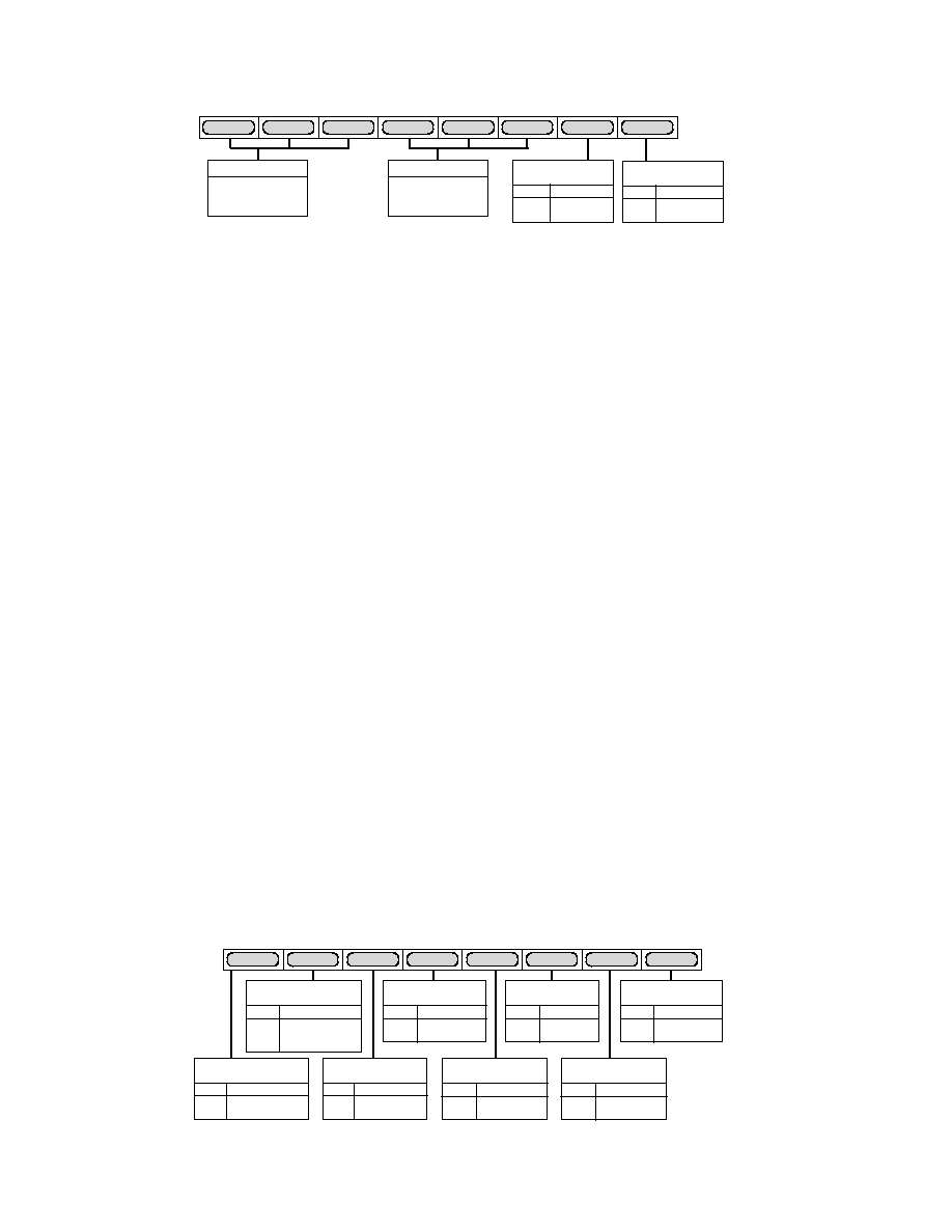
ADV7192
34
REV. A
Mode Register 6
MR6 (MR67MR60)
(Address (SR4SR0) = 06H)
Mode Register 6 is a 8-bit-wide register. Figure 45 shows the
various operations under the control of Mode Register 6.
MR6 BIT DESCRIPTION
Power-Up Sleep Mode Control (MR60)
After
RESET is applied this control is enabled (MR60 = 0) if
both SCRESET/RTC/TR and NTSC_PAL pins are tied high.
The ADV7192 will then power up in Sleep Mode to facilitate
low power consumption before the I
2
C is initialized. When this
control is disabled (MR60 = 1, via the I
2
C) Sleep Mode control
passes to Sleep Mode Control, MR27.
PPL Enable Control (MR61)
The PLL control should be enabled (MR61 = 0 ) when 4
×
Oversampling is enabled (MR16 = 1). When this bit is toggled,
it is also used to reset the PLL.
Reserved (MR62, MR63, MR64)
A Logical 0 must be written to these bits.
Field Counter (MR65, MR66, MR67)
These three bits are read only bits. The field count can be read
back over the I
2
C interface. In NTSC mode the field count goes
from 03, in PAL Mode from 07.
MODE REGISTER 7
MR7 (MR77MR70)
(Address (SR4SR0) = 07H)
Mode Register 7 is a 8-bit-wide register. Figure 46 shows the
various operations under the control of Mode Register 7.
MR7 BIT DESCRIPTION
Color Control Enable (MR70)
This bit is used to enable control of contrast and saturation of
color. If this bit is set (1) color controls are enabled (Contrast
Control Register, U-Scale Register, V-Scale Register). If this bit
is set (0), the color control features are disabled.
Luma Saturation Control (MR71)
When this bit is set (1), the luma signal will be clipped if it reaches
a limit that corresponds to an input luma value of 255 (after
scaling by the Contrast Control Register). This prevents the
chrominance component of the composite video signal being
clipped if the amplitude of the luma is too high. When this bit is
set (0), this control is disabled.
Hue Adjust Control (MR72)
This bit is used to enable hue adjustment on the composite and
chroma output signals of the ADV7192. When this bit is set (1),
the hue of the color is adjusted by the phase offset described in
the Hue Adjust Control Register. When this bit is set (0), hue
adjustment is disabled.
Brightness Enable Control (MR73)
This bit is used to enable brightness control on the ADV7192.
The actual brightness level is programmed in the Brightness
Control Register. This value or set-up level is added to the scaled
Y data. When this bit is set (1), brightness control is enabled.
When this bit is set (0), brightness control is disabled.
Sharpness Filter Enable (MR74)
This bit is used to enable the sharpness control of the luminance
signal on the ADV7192 (Luma Filter Select has to be set to
Extended, MR04MR02 = 100). The various responses of the
filter are determined by the Sharpness Control Register. When this
bit is set (1), the luma response is altered by the amount described
in the Sharpness Control Register. When this bit is set (0), the
sharpness control is disabled. See Internal Filter Response section
for luma signal responses.
CSO_HSO Output Control (MR75)
This bit is used to determine whether
HSO or CSO TTL output
signal is output at the
CSO_HSO pin. If this bit is set (1), the
CSO TTL signal is output. If this bit is set (0), the HSO TTL
signal is output.
TTX Input/CLAMP
VSO Output (MR76)
This bit controls whether Pin 62 is configured as an output or as
an input pin. A 1 selects Pin 62 to be an output for CLAMP or
VSO functionality. A 0 selects this pin as a TTX input pin.
MR77
MR76
MR75
MR74
MR73
MR72
MR71
MR70
0
DISABLE
1
ENABLE
MR74
SHARPNESS FILTER
ENABLE
0
VSO OUTPUT
1
CLAMP OUTPUT
MR77
CLAMP/
VSO
SELECT
0
DISABLE
1
ENABLE
MR70
COLOR CONTROL
ENABLE
CSO_HSO
OUTPUT CONTROL
0
HSO OUT
1
CSO OUT
MR75
0
DISABLE
1
ENABLE
MR72
HUE ADJUST
CONTROL
0
DISABLE
1
ENABLE
MR73
BRIGHTNESS
ENABLE CONTROL
0
DISABLE
1
ENABLE
MR71
LUMA SATURATION
CONTROL
MR76
TTX INPUT/CLAMP
VSO
OUTPUT CONTROL
0
TTX INPUT
1
CLAMP/
VSO
OUTPUT
Figure 46. Mode Register 7, MR7
MR67
MR66
MR65
MR64
MR63
MR62
MR61
MR60
0
ENABLED
1
DISABLED
MR60
POWER-UP SLEEP
MODE CONTROL
0
ENABLED
1
DISABLED
MR61
PLL ENABLE
CONTROL
ZERO MUST
BE WRITTEN
TO THESE BITS
MR64 MR63 MR62
FIELD COUNTER
MR67 MR66 MR65
Figure 45. Mode Register 6, MR6
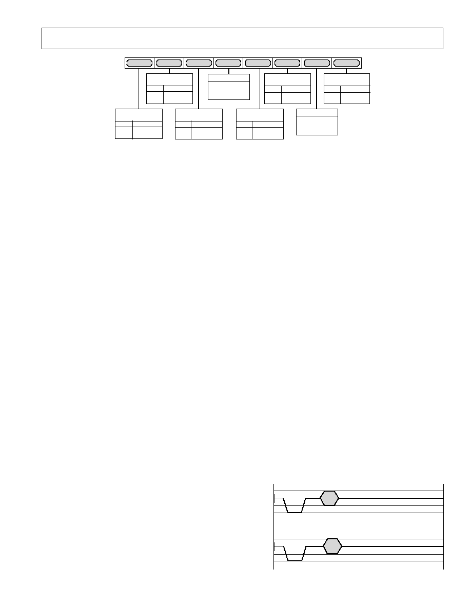
ADV7192
35
REV. A
CLAMP/
VSO Select (MR77)
This bit is used to select the functionality of Pin 62. Setting this
bit to 1 selects CLAMP as the output signal. A 0 selects
VSO
as the output signal. Since this pin is also shared with the TTX
functionality, TTX Input/CLAMP
VSO Output has to be set
accordingly (MR76).
MODE REGISTER 8
MR8 (MR87MR80)
(Address (SR4SR0) = 08H)
Mode Register 8 is an 8-bit-wide register. Figure 47 shows the
various operations under the control of Mode Register 8.
MR8 BIT DESCRIPTION
Progressive Scan Control (MR80)
This control enables the progressive scan inputs on pins
Y(0)/P8Y(7)/P15, Y(8)Y(9), Cr(0)Cr(9), Cb(0)Cb(9). To
enable this control MR80 has to be set to 1. It is assumed that
the incoming Y data contains all necessary sync information.
Note: Simultaneous progressive scan input and 16-bit pixel input
is not possible.
Reserved (MR81)
A 0 must be written to this bit.
Double Buffer Control (MR82)
Double Buffering can be enabled or disabled on the Contrast
Control Register, U Scale Register, V Scale Register, Hue Adjust
Control Register, Closed Captioning Register, Brightness Control
Register, Gamma Curve Select Bit and the Macrovision Regis-
ters. Double Buffer is not available in Master Mode.
16-Bit Pixel Port (MR83)
This bit controls if the ADV7192 is operated in 8-bit or 16-bit
mode. In 8-bit mode the input data will be set up on Pins P0P7.
In 16-bit mode the first eight bits are set up on Pin 310, with
LSB on Pin 3. The second eight bits are set up on Pin 1320.
Reserved (MR84)
A Logic 0 must be written to this bit.
DNR Enable Control (MR85)
To enable the DNR process this bit has to be set to 1. If this bit
is set to other DNR processing is bypassed. For further informa-
tion on DNR controls see DNR Mode Control section.
Gamma Enable Control (MR86)
To enable the programmable gamma correction this bit has to be
set to enabled (MR86 = 1). For further information on Gamma
Correction controls see Gamma Correction Registers section.
Gamma Curve Select Control (MR87)
This bit selects which of the two programmable gamma curves is
to be used. When setting MR87 to 0, the gamma correction curve
selected is Curve A. Otherwise, Curve B is selected. Each curve
will have to be programmed by the user. For further information
on Gamma Correction controls see Gamma Correction Regis-
ters section.
MODE REGISTER 9
MR9 (MR97MR90)
(Address (SR4SR0) = 09H)
Mode Register 9 is an 8-bit-wide register. Figure 49 shows the
various operations under the control of Mode Register 9.
MR9 BIT DESCRIPTION
Undershoot Limiter (MR90MR91)
This control ensures that no luma video data will go below a
programmable level. This prevents any synchronization problems
due to luma signals going below the blanking level. Available
limit levels are 1.5 IRE, 6 IRE, 11 IRE. Note that this facility is
only available in 4
× Oversampling mode (MR16 = 1). When the
device is operated in 2
× Oversampling mode (MR16 = 0) or RGB
output without RGB sync are selected, the minimum luma level is
set in Timing Register 0, TR06 (Min Luma Control).
Black Burst Y DAC (MR92)
It is possible to output a Black Burst signal from the DAC
which is selected to be the Luma DAC (MR22, MR21, MR20).
This signal can be useful for locking two video sources together
using professional video equipment. See also Black Burst Out-
put section.
Black Burst Luma (MR93)
It is possible to output a Black Burst signal from the DAC which
is selected to be the Y-DAC (MR22, MR21, MR20). This signal
can be useful for locking two video sources together using pro-
fessional video equipment. See also Black Burst Output section.
20 IRE
0 IRE
20 IRE
40 IRE
21.5 IRE
0 IRE
21.5 IRE
43 IRE
3.58MHz
COLOR BURST
(9 CYCLES)
4.43MHz
COLOR BURST
(10 CYCLES)
NTSC BLACK BURST SIGNAL
PAL BLACK BURST SIGNAL
Figure 48. Black Burst Signals for PAL and NTSC Standards
ZERO SHOULD
BE WRITTEN
TO THIS BIT
MR84
MR87
MR86
MR85
MR84
MR83
MR82
MR81
MR80
MR83
16-PIXEL
PORT CONTROL
0
DISABLE
1
ENABLE
DNR ENABLE
CONTROL
MR85
0
DISABLE
1
ENABLE
0
DISABLE
1
ENABLE
MR82
DOUBLE BUFFER
CONTROL
0
DISABLE
1
ENABLE
MR86
GAMMA ENABLE
CONTROL
0
CURVE A
1
CURVE B
MR87
GAMMA CURVE
SELECT CONTROL
ZERO SHOULD
BE WRITTEN
TO THIS BIT
MR81
0
DISABLE
1
ENABLE
MR80
PROGRESSIVE
SCAN CONTROL
Figure 47. Mode Register 8, MR8
ADV7192
36
REV. A
Chroma Delay Control (MR94MR95)
The Chroma signal can be delayed by up to 8 clock cycles at
27 MHz using MR9495. For further information see also
Chroma/Luma Delay Section.
TIMING REGISTER 0 (TR07TR00)
(Address (SR4SR0) = 0AH)
Figure 50 shows the various operations under the control of
Timing Register 0. This register can be read from as well as
written to.
TR0 BIT DESCRIPTION
Master/Slave Control (TR00)
This bit controls whether the ADV7192 is in master or slave mode.
Timing Mode Selection (TR01TR02)
These bits control the timing mode of the ADV7192. These
modes are described in more detail in the Video Timing Descrip-
tion section of the data sheet.
BLANK Input Control (TR03)
This bit controls whether the
BLANK input is used to accept
blank signals or whether blank signals are internally generated.
Note: When this input pin is tied high (to 5 V), the input is dis-
abled regardless of the register setting. It, therefore, should be
tied low (to Ground) to allow control over the I
2
C register.
Luma Delay (TR04TR05)
The luma signal can be delayed by up to 222 ns (or six clock
cycles at 27 MHz) using TR04TR05. For further information
see Chroma/Luma Delay section.
Min Luminance Value (TR06)
This bit is used to control the minimum luma output value
by the ADV7192 in 2
× Oversampling mode and 4× Oversampling
mode. When this bit is set to a Logic 1, the luma is limited to
7IRE below the blank level. When this bit is set to (0), the luma
value can be as low as the sync bottom level.
Timing Register Reset (TR07)
Toggling TR07 from low to high and low again resets the inter-
nal timing counters. This bit should be toggled after power-up,
reset or changing to a new timing mode.
TIMING REGISTER 1 (TR17TR10)
(Address (SR4SR0) = 0BH)
Timing Register 1 is a 8-bit-wide register.
Figure 51 shows the various operations under the control of
Timing Register 1. This register can be read from as well written
to. This register can be used to adjust the width and position of
the master mode timing signals.
TR1 BIT DESCRIPTION
HSYNC Width (TR10TR11)
These bits adjust the
HSYNC pulsewidth.
T
PCLK
= one clock cycle at 27 MHz.
HSYNC to VSYNC Delay (TR13TR12)
These bits adjust the position of the
HSYNC output relative to
the VSYNC output.
T
PCLK
= one clock cycle at 27 MHz.
HSYNC to VSYNC Rising Edge Delay (TR14TR15)
When the ADV7192 is in Timing Mode 1, these bits adjust the
position of the HSYNC output relative to the VSYNC output
rising edge.
T
PCLK
= one clock cycle at 27 MHz.
VSYNC Width (TR14TR15)
When the ADV7192 is configured in Timing Mode 2, these bits
adjust the
VSYNC pulsewidth.
T
PCLK
= one clock cycle at 27 MHz.
HSYNC to Pixel Data Adjust (TR16TR17)
This enables the
HSYNC to be adjusted with respect to the
pixel data. This allows the Cr and Cb components to be swapped.
MR97
MR96
MR95
MR94
MR93
MR92
MR91
MR90
ZERO MUST
BE WRITTEN
TO THESE BITS
MR97 MR96
CHROMA
DELAY CONTROL
MR95 MR94
0 0 0ns DELAY
0
1
148ns DELAY
1
0
296ns DELAY
1
1
RESERVED
UNDERSHOOT
LIMITER
MR91 MR90
0 0 DISABLED
0
1
11 IRE
1
0
6 IRE
1
1
1.5 IRE
0
DISABLE
1
ENABLE
MR93
BLACK BURST
LUMA DAC
BLACK BURST
Y DAC
0
DISABLE
1
ENABLE
MR92
Figure 49. Mode Register 9 (MR9)
TR07
TR06
TR05
TR04
TR03
TR02
TR01
TR00
0
LUMA MIN =
SYNC BOTTOM
1
LUMA MIN =
BLANK 7.5 IRE
TR06
MIN LUMINANCE VALUE
0
ENABLE
1
DISABLE
TR03
BLANK INPUT
CONTROL
TIMING
REGISTER RESET
TR07
0
SLAVE TIMING
1
MASTER TIMING
TR00
MASTER / SLAVE
CONTROL
LUMA DELAY
TR05 TR04
0 0 0ns DELAY
0
1
74ns DELAY
1
0
148ns DELAY
1
1
222ns DELAY
TR02 TR01
0 0 MODE 0
0
1
MODE 1
1
0
MODE 2
1
1
MODE 3
TIMING MODE
SELECTION
Figure 50. Timing Register 0
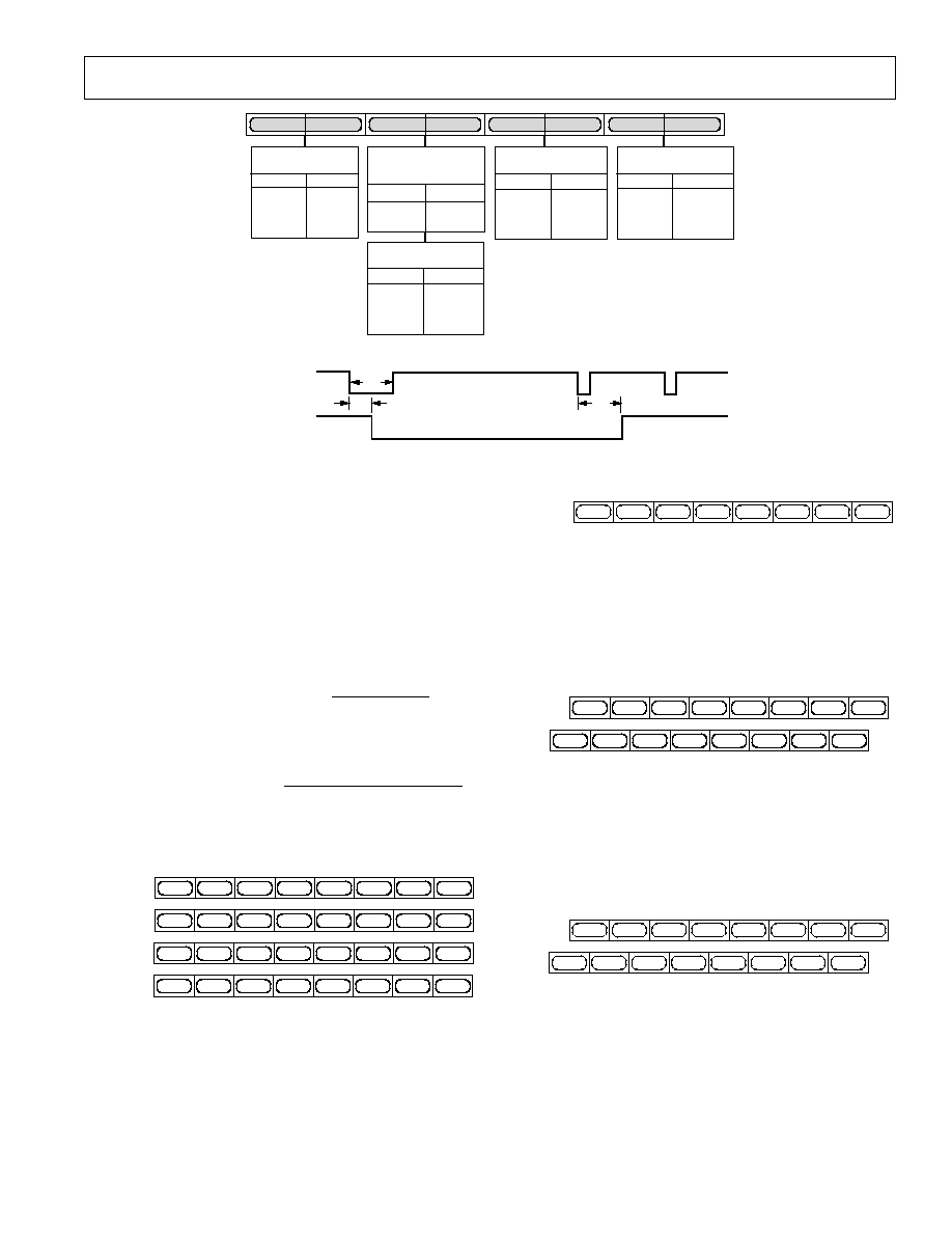
ADV7192
37
REV. A
This adjustment is available in both master and slave timing
modes.
T
PCLK
= one clock cycle at 27 MHz.
SUBCARRIER FREQUENCY REGISTERS 30
(FSC31FSC0) (Address (SR4SR0) = 0CH0FH)
These 8-bit-wide registers are used to set up the Subcarrier Fre-
quency. The value of these registers are calculated by using the
following equation:
Subcarrier Frequency
f
f
SCF
CLK
Register
=
(
)
×
2
1
32
Example: NTSC Mode, f
CLK
= 27 MHz, f
SCF
= 3.5795454 MHz
Subcarrier Frequency alue
V
=
(
)
×
×
×
2
1
3 5795454
10
27
10
32
6
6
.
Subcarrier Register Value = 21F07C16 Hex
Figure 52 shows how the frequency is set up by the four registers.
FSC31
FSC30
FSC29
FSC28
FSC27
FSC26
FSC25
FSC24
SUBCARRIER
FREQUENCY
REG 3
FSC23
FSC22
FSC21
FSC20
FSC19
FSC18
FSC17
FSC16
SUBCARRIER
FREQUENCY
REG 2
SUBCARRIER
FREQUENCY
REG 1
FSC7
FSC6
FSC5
FSC4
FSC3
FSC2
FSC1
FSC0
SUBCARRIER
FREQUENCY
REG 0
FSC15
FSC14
FSC13
FSC12
FSC11
FSC10
FSC9
FSC8
Figure 52. Subcarrier Frequency Registers
SUBCARRIER PHASE REGISTER (FPH7FPH0)
(Address (SR4SR0) = 10H)
This 8-bit-wide register is used to set up the Subcarrier Phase.
Each bit represents 1.41
°. For normal operation this register is
set to 00Hex.
FPH7
FPH6
FPH5
FPH4
FPH3
FPH2
FPH1
FPH0
SUBCARRIER
PHASE
REGISTER
Figure 53. Subcarrier Phase Register
CLOSED CAPTIONING EVEN FIELD
DATA REGISTER 10 (CCD15CCD0)
(Address (SR4SR0) = 1112H)
These 8-bit-wide registers are used to set up the closed captioning
extended data bytes on Even Fields. Figure 54 shows how the
high and low bytes are set up in the registers.
CCD15
CCD14
CCD13
CCD12
CCD11
CCD10
CCD9
CCD8
BYTE 1
CCD7
CCD6
CCD5
CCD4
CCD3
CCD2
CCD1
CCD0
BYTE 0
Figure 54. Closed Captioning Extended Data Register
CLOSED CAPTIONING ODD FIELD
DATA REGISTER 10 (CED15-CED0)
(Subaddress (SR4SR0) = 1314H)
These 8-bit-wide registers are used to set up the closed captioning
data bytes on Odd Fields. Figure 55 shows how the high and low
bytes are set up in the registers.
CED15
CED14
CED13
CED12
CED11
CED10
CED9
CED8
BYTE 1
CED7
CED6
CED5
CED4
CED3
CED2
CED1
CED0
BYTE 0
Figure 55. Closed Captioning Data Register
NTSC PEDESTAL/PAL TELETEXT CONTROL
REGISTERS 30
(PCE150, PCO150)/(TXE150, TXO150)
(Subaddress (SR4SR0) = 1518H)
These 8-bit-wide registers are used to enable the NTSC pedestal/
PAL Teletext on a line-by-line basis in the vertical blanking
interval for both odd and even fields. Figures 56 and 57 show
the four control registers. A Logic 1 in any of the bits of these
TR17
TR16
TR15
TR14
TR13
TR12
TR11
TR10
TR17 TR16
0 0 0 T
PCLK
0
1
1 T
PCLK
1
0
2 T
PCLK
1
1
3 T
PCLK
HSYNC TO PIXEL
DATA ADJUST
TR15 TR14 T
C
0 T
B
1
T
B
+ 32 s
HSYNC TO VSYNC
RISING EDGE DELAY
(MODE 1 ONLY)
TR13 TR12 T
B
0 0 0 T
PCLK
0
1
4 T
PCLK
1
0
8 T
PCLK
1
1
18 T
PCLK
HSYNC TO
VSYNC DELAY
TR11 TR10 T
A
0 0 1 T
PCLK
0
1
4 T
PCLK
1
0
16 T
PCLK
1
1
128 T
PCLK
HSYNC WIDTH
TR15 TR14
0 0 1 T
PCLK
0
1
4 T
PCLK
1
0
16 T
PCLK
1
1
128 T
PCLK
VSYNC WIDTH
(MODE 2 ONLY)
LINE 313
LINE 314
LINE 1
T
B
T
A
T
C
VSYNC
HSYNC
TIMING MODE 1 (MASTER/PAL)
Figure 51. Timing Register 1
ADV7192
38
REV. A
registers has the effect of turning the Pedestal OFF on the equiva-
lent line when used in NTSC. A Logic 1 in any of the bits of
these registers has the effect of turning Teletext ON on the
equivalent line when used in PAL.
PCO7
PCO6
PCO5
PCO4
PCO3
PCO2
PCO1
PCO0
FIELD 1/3
PCO15
PCO14
PCO13
PCO12
PCO11
PCO10
PCO9
PCO8
FIELD 1/3
PCE15
PCE14
PCE13
PCE12
PCE11
PCE10
PCE9
PCE8
PCE7
PCE6
PCE5
PCE4
PCE3
PCE2
PCE1
PCE0
LINE 17 LINE 16
LINE 15
LINE 14
LINE 13
LINE 12
LINE 11
LINE 10
LINE 25 LINE 24
LINE 23
LINE 22
LINE 21 LINE 20
LINE 19
LINE 18
LINE 17 LINE 16
LINE 15
LINE 14
LINE 13
LINE 12
LINE 11
LINE 10
LINE 25 LINE 24
LINE 23
LINE 22
LINE 21 LINE 20
LINE 19
LINE 18
FIELD 2/4
FIELD 2/4
Figure 56. Pedestal Control Registers
TXO7
TXO6
TXO5
TXO4
TXO3
TXO2
TXO1
TXO0
FIELD 1/3
TXO15
TXO14
TXO13
TXO12
TXO11
TXO10
TXO9
TXO8
FIELD 1/3
TXE15
TXE14
TXE13
TXE12
TXE11
TXE10
TXE9
TXE8
TXE7
TXE6
TXE5
TXE4
TXE3
TXE2
TXE1
TXE0
LINE 14 LINE 13
LINE 12
LINE 11
LINE 10
LINE 9
LINE 8
LINE 7
LINE 22 LINE 21
LINE 20
LINE 19
LINE 18 LINE 17
LINE 16
LINE 15
FIELD 2/4
FIELD 2/4
LINE 14 LINE 13
LINE 12
LINE 11
LINE 10
LINE 9
LINE 8
LINE 7
LINE 22 LINE 21
LINE 20
LINE 19
LINE 18 LINE 17
LINE 16
LINE 15
Figure 57. Teletext Control Registers
TELETEXT REQUEST CONTROL REGISTER TC07
(TC07TC00)
(Address (SR4SR0) = 1CH)
Teletext Control Register is an 8-bit-wide register. See Figure 58.
TTXREQ Falling Edge Control (TC00TC03)
These bits control the position of the falling edge of TTXREQ.
It can be programmed from zero clock cycles to a maximum of 15
clock cycles. This controls the active window for Teletext data.
Increasing this value reduces the amount of Teletext bits below the
default of 360. If Bits TC00TC03 are 00Hex when Bits TC04
TC07 are changed then the falling edge of TTREQ will track that
of the rising edge (i.e., the time between the falling and rising
edge remains constant).
PCLK = clock cycle at 27 MHz.
TTXREQ Rising Edge Control (TC04TC07)
These bits control the position of the rising edge of TTXREQ.
It can be programmed from zero clock cycles to a maximum of 15
clock cycles.
PCLK = clock cycle at 27 MHz.
TC07
TC06
TC05
TC04
TC03
TC02
TC01
TC00
TC03 TC02 TC01 TC00
0 0 0
0
0 PCLK
0
0 0 1
1 PCLK
''
'' '' ''
'' PCLK
1
1 1 0
14 PCLK
1
1 1 1
15 PCLK
TTXREQ
FALLING EDGE CONTROL
TC07 TC06 TC05 TC04
0 0 0
0
0 PCLK
0
0 0 1
1 PCLK
''
'' '' ''
'' PCLK
1
1 1 0
14 PCLK
1
1 1 1
15 PCLK
TTXREQ
RISING EDGE CONTROL
Figure 58. Teletext Control Register
CGMS_WSS REGISTER 0 C/W0 (C/W07C/W00)
(Address (SR4SR0) = 19H)
CGMS_WSS register 0 is an 8-bit-wide register. Figure 59 shows
the operations under control of this register.
C/W0 BIT DESCRIPTION
CGMS Data Bits (C/W00C/W03)
These four data bits are the final four bits of CGMS data out-
put stream. Note it is CGMS data ONLY in these bit positions,
i.e., WSS data does not share this location.
CGMS CRC Check Control (C/W04)
When this bit is enabled (1), the last six bits of the CGMS data,
i.e., the CRC check sequence, is internally calculated by the
ADV7192. If this bit is disabled (0) the CRC values in the reg-
ister are output to the CGMS data stream.
CGMS Odd Field Control (C/W05)
When this bit is set (1), CGMS is enabled for odd fields. Note
this is only valid in NTSC mode.
CGMS Even Field Control (C/W06)
When this bit is set (1), CGMS is enabled for even fields. Note
this is only valid in NTSC mode.
WSS Control (C/W07)
When this bit is set (1), wide screen signalling is enabled. Note
this is only valid in PAL mode.
CGMS_WSS REGISTER 1 C/W1 (C/W17C/W10)
(Address (SR4SR0) = 1AH)
CGMS_WSS register 1 is an 8-bit-wide register. Figure 60 shows
the operations under control of this register.
C/W1 BIT DESCRIPTION
CGMS/WSS Data (C/W10C/W15)
These bit locations are shared by CGMS data and WSS data. In
NTSC mode these bits are CGMS data. In PAL mode these bits
are WSS data.
C/W07
C/W06
C/W05
C/W04
C/W03
C/W02
C/W01
C/W00
0
DISABLE
1
ENABLE
C/W07
WSS CONTROL
0
DISABLE
1
ENABLE
C/W05
CGMS ODD FIELD
CONTROL
0
DISABLE
1
ENABLE
C/W06
CGMS EVEN FIELD
CONTROL
0
DISABLE
1
ENABLE
C/W04
CGMS CRC CHECK
CONTROL
C/W03 C/W00
CGMS DATA BITS
Figure 59. CGMS_WSS Register 0
ADV7192
39
REV. A
CGMS Data (C/W16C/W17)
These bits are CGMS data bits only.
C/W17
C/W16
C/W15
C/W14
C/W13
C/W12
C/W11
C/W10
C/W15 C/W10
CGMS/WSS DATA
C/W17 C/W16
CGMS DATA
Figure 60. CGMS_WSS Register 1
CGMS_WSS REGISTER 2
C/W1 (C/W27C/W20)
(Address (SR4SR0) = 1BH)
CGMS_WSS Register 2 is an 8-bit-wide register. Figure 61 shows
the operations under control of this register.
C/W2 BIT DESCRIPTION
CGMS/WSS Data (C/W20C/W27)
These bit locations are shared by CGMS data and WSS data. In
NTSC mode these bits are CGMS data. In PAL mode these bits
are WSS data.
C/W27 C/W20
CGMS/WSS DATA
C/W27
C/W26
C/W25
C/W24
C/W23
C/W22
C/W21
C/W20
Figure 61. CGMS_WSS Register 2
CONTRAST CONTROL REGISTER (CC00CC07)
(Address (SR4SR0) = 1DH)
The contrast control register is an 8-bit-wide register used to
scale the Y output levels. Figure 62 shows the operation under
control of this register.
Y Scale Value (CC00CC07)
These eight bits represent the value required to scale the Y pixel
data from 0.0 to 1.5 of its initial level. The value of these eight
bits is calculated using the following equation:
Y Scale Value = Scale Factor
× 128
Example:
Scale Factor = 1.18
Y Scale Value = 1.18
× 128 = 151.04
Y Scale Value = 151 (rounded to the nearest integer)
Y Scale Value = 10010111
b
Y Scale Value = 97
h
CC07 CC00
Y SCALE VALUE
CC07
CC06
CC05
CC04
CC03
CC02
CC01
CC00
Figure 62. Contrast Control Register
COLOR CONTROL REGISTERS 12 (CC1CC2)
(Address (SR4SR0) = 1EH1FH)
The color control registers are 8-bit-wide registers used to scale
the U and V output levels. Figure 63 shows the operations under
control of these registers.
CC17 CC10
U SCALE VALUE
CC17
CC16
CC15
CC14
CC13
CC12
CC11
CC10
CC27 CC20
V SCALE VALUE
CC27
CC26
CC25
CC24
CC23
CC22
CC21
CC20
Figure 63. Color Control Registers
CC1 BIT DESCRIPTION
U Scale Value (CC10CC17)
These eight bits represent the value required to scale the U level
from 0.0 to 2.0 of its initial level. The value of these eight bits is
calculated using the following equation:
U Scale Value = Scale Factor
× 128
Example:
Scale Factor = 1.18
U Scale Value = 1.18
× 128 = 151.04
U Scale Value = 151 (rounded to the nearest integer)
U Scale Value = 10010111
b
U Scale Value = 97
h
CC2 BIT DESCRIPTION
V Scale Value (CC20CC27)
These eight bits represent the value required to scale the V pixel
data from 0.0 to 2.0 of its initial level. The value of these eight
bits is calculated using the following equation:
V Scale Value = Scale Factor
× 128
Example:
Scale Factor = 1.18
V Scale Value = 1.18
× 128 = 151.04
V Scale Value = 151 (rounded to the nearest integer)
V Scale Value = 10010111
b
V Scale Value = 97
h
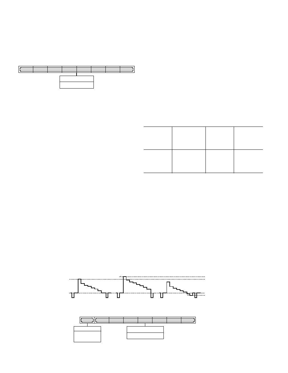
ADV7192
40
REV. A
HUE ADJUST CONTROL REGISTER (HCR)
(Address (SR5SR0) = 20H)
The hue control register is an 8-bit-wide register used to adjust
the hue on the composite and chroma outputs. Figure 64 shows
the operation under control of this register.
HCR7 HCR0
HUE ADJUST VALUE
HCR7
HCR6
HCR5
HCR4
HCR3
HCR2
HCR1
HCR0
Figure 64. Hue Control Register
HCR BIT DESCRIPTION
Hue Adjust Value (HCR0HCR7)
These eight bits represent the value required to vary the hue of
the video data, i.e., the variance in phase of the subcarrier during
active video with respect to the phase of the subcarrier during
the colorburst. The ADV7192 provides a range of
±22.5° incre-
ments of 0.17578125
°. For normal operation (zero adjustment),
this register is set to 80Hex. FFHex and 00Hex represent the
upper and lower limit (respectively) of adjustment attainable.
Hue Adjust [
°] = 0.17578125°
× (HCR
d
128); for positive Hue
Adjust Value
Example:
To adjust the hue by 4
° write 97
h
to the Hue Adjust Control
Register:
(4/0.17578125) + 128 = 151
d
* = 97
h
To adjust the hue by (4
°) write 69
h
to the Hue Adjust Control
Register:
(4/0.17578125) + 128 = 105
d
* = 69
h
*Rounded to the nearest integer.
BRIGHTNESS CONTROL REGISTER (BCR)
(Address (SR5SR0) = 21H)
The brightness control register is an 8-bit-wide register which
allows brightness control. Figure 65 shows the operation under
control of this register.
BCR BIT DESCRIPTION
Brightness Value (BCR0BCR6)
Seven bits of this 8-bit-wide register are used to control the
brightness level. The brightness is controlled by adding a pro-
grammable setup level onto the scaled Y data. This brightness
level can be a positive or negative value.
The programmable brightness levels in NTSC, without pedestal,
and PAL are max 15 IRE and min 7.5 IRE, in NTSC pedestal
max 22.5 IRE and min 0 IRE.
Table IV. Brightness Control Register Value
Setup
Setup
Brightness
Level in
Level in
Setup
Control
NTSC with
NTSC No
Level in
Register
Pedestal
Pedestal
PAL
Value
22.5 IRE
15 IRE
15 IRE
1E
h
15 IRE
7.5 IRE
7.5 IRE
0F
h
7.5 IRE
0 IRE
0 IRE
00
h
0 IRE
7.5 IRE
7.5 IRE
71
h
NOTE
Values in the range from 3F
h
to 44
h
might result in an invalid output signal.
EXAMPLE
1. Standard: NTSC with Pedestal. To add 20 IRE brightness level write 28
h
into the Brightness Control Register:
[Brightness Control Register Value]
h
= [IRE Value
2.015631]
h
= [20 2.015631]
h
= [40.31262]
h
= 28
h
2. Standard: PAL. To add 7 IRE brightness level write 72
h
into the Brightness Control Register:
[|IRE Value| 2.015631]
= [7 2.015631]
= [14.109417] = 0001110
b
[0001110] into two's complement
= 1110010
b
= 72
h
BCR6 BCR0
BRIGHTNESS VALUE
BCR7
ZERO MUST BE
WRITTEN TO
THIS BIT
BCR7
BCR6
BCR5
BCR4
BCR3
BCR2
BCR1
BCR0
100 IRE
0 IRE
+7.5 IRE
7.5 IRE
NTSC WITHOUT PEDESTAL
NO SETUP VALUE
ADDED
POSITIVE SETUP
VALUE ADDED
WRITE TO BRIGHTNESS
CONTROL REGISTER: 12
h
NEGATIVE SETUP
VALUE ADDED
WRITE TO BRIGHTNESS
CONTROL REGISTER: 6E
h
Figure 65. Brightness Control Register
ADV7192
41
REV. A
SHARPNESS RESPONSE REGISTER (PR)
(Address (SR5SR0) = 22H)
The sharpness response register is an 8-bit-wide register. The
four MSBs are set to 0. The four LSBs are written to in order to
select a desired filter response. Figure 66 shows the operation
under control of this register.
PR BIT DESCRIPTION
Sharpness Response Value (PR3PR0)
These four bits are used to select the desired luma filter response. The
option of twelve responses is given supporting a gain boost/
attenuation in the range 4 dB to +4 dB. The value 12 (1100)
written to these four bits corresponds to a boost of +4 dB while
the value 0 (0000) corresponds to 4 dB. For normal operation
these four bits are set to 6 (0110). Note: Luma Filter Select has
to be set to Extended Mode and Sharpness Filter Control has to
be enabled for settings in the Sharpness Control Register to
take effect (MR0204 = 100; MR74 = 1).
Reserved (PR4PR7)
A Logical 0 must be written to these bits.
PR3 PR0
SHARPNESS
RESPONSE VALUE
ZERO MUST BE
WRITTEN TO
THESE BITS
PR7 PR4
PR7
PR6
PR5
PR4
PR3
PR2
PR1
PR0
Figure 66. Sharpness Response Register
DNR REGISTERS 20
(DNR2DNR0)
(Address (SR5SR0) = 23H25H)
The Digital Noise Reduction Registers are three 8-bit-wide
register. They are used to control the DNR processing. See
Digital Noise Register section.
Coring Gain Border (DNR00DNR03)
These four bits are assigned to the gain factor applied to border
areas.
In DNR Mode the range of gain values is 01, in increments of
1/8. This factor is applied to the DNR filter output which lies
below the set threshold range. The result is then subtracted
from the original signal.
In DNR Sharpness Mode the range of gain values is 00.5, in
increments of 1/16. This factor is applied to the DNR filter output
which lies above the threshold range.
The result is added to the original signal.
Coring Gain Data (DNR04DNR07)
These four bits are assigned to the gain factor applied to the
luma data inside the MPEG pixel block.
In DNR Mode the range of gain values is 01, in increments of
1/8. This factor is applied to the DNR filter output which lies
below the set threshold range. The result is then subtracted
from the original signal.
In DNR Sharpness Mode the range of gain values is 00.5, in
increments of 1/16. This factor is applied to the DNR filter out-
put which lies above the threshold range. The result is added to
the original signal.
Figures 67 and 68 show the various operations under the control
of DNR Register 0.
DNR07
DNR06
DNR05
DNR04
DNR03
DNR02
DNR01
DNR00
CORING GAIN DATA
DNR DNR DNR DNR
07 06 05 04
0 0
0
0
0
0
0
1
+1/16
0
0
1
0
+2/16
0
0
1
1
+3/16
0
1
0
0
+4/16
0
1
0
1
+5/16
0
1
1
0
+6/16
0
1
1
1
+7/16
1
0
0
0
+8/16
CORING GAIN BORDER
DNR DNR DNR DNR
03 02 01 00
0 0
0
0
0
0
0
1
+1/16
0
0
1
0
+2/16
0
0
1
1
+3/16
0
1
0
0
+4/16
0
1
0
1
+5/16
0
1
1
0
+6/16
0
1
1
1
+7/16
1
0
0
0
+8/16
Figure 67. DNR Register 0 in DNR Sharpness Mode
CORING GAIN DATA
DNR DNR DNR DNR
07 06 05 04
0 0
0
0
0
0
0
0
1
1/8
0
0
1
0
2/8
0
0
1
1
3/8
0
1
0
0
4/8
0
1
0
1
5/8
0
1
1
0
6/8
0
1
1
1
7/8
1
0
0
0
1
CORING GAIN BORDER
DNR DNR DNR DNR
03 02 01 00
0 0
0
0
0
0
0
0
1
1/8
0
0
1
0
2/8
0
0
1
1
3/8
0
1
0
0
4/8
0
1
0
1
5/8
0
1
1
0
6/8
0
1
1
1
7/8
1
0
0
0
1
DNR07
DNR06
DNR05
DNR04
DNR03
DNR02
DNR01
DNR00
Figure 68. DNR Register 0 in DNR Mode
DNR1 BIT DESCRIPTION
DNR Threshold (DNR10DNR15)
These six bits are used to define the threshold value in the range
of 0 to 63. The range is an absolute value.
Border Area (DNR16)
In setting DNR16 to a Logic 1 the block transition area can be
defined to consist of four pixels. If this bit is set to a Logic 0 the
border transition area consists of two pixels, where one pixel
refers to two clock cycles at 27 MHz.
Block Size Control (DNR17)
This bit is used to select the size of the data blocks to be processed
(see Figure 69). Setting the block size control function to a Logic 1
defines a 16
× 16 pixel data block, a Logic 0 defines an 8 × 8 pixel
data block, where one pixel refers to two clock cycles at 27 MHz.
720 485 PIXELS
(NTSC)
2 PIXEL
BORDER DATA
8 8
PIXEL BLOCK
8 8
PIXEL BLOCK
Figure 69. MPEG Block Diagram
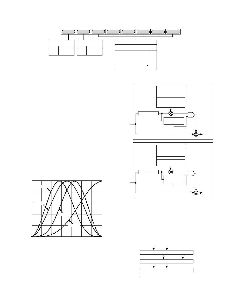
ADV7192
42
REV. A
DNR17
DNR16
DNR15
DNR14
DNR13
DNR12
DNR11
DNR10
DNR THRESHOLD
DNR DNR DNR DNR DNR DNR
15 14 13 12 11 10
0 0
0
0
0
0
0
0
0
0
0
0
1
1
·
·
·
·
·
·
·
·
·
·
·
·
·
·
·
·
·
·
·
·
·
1
1
1
1
1
0
62
1
1
1
1
1
1
63
0
2 PIXELS
1
4 PIXELS
DNR16
BORDER AREA
0
8 PIXELS
1
16 PIXELS
DNR17
BLOCK SIZE
CONTROL
Figure 70. DNR Register 1
DNR2 BIT DESCRIPTION
DNR Input Select (DNR20DNR22)
Three bits are assigned to select the filter which is applied to the
incoming Y data. The signal which lies in the passband of the
selected filter is the signal which will be DNR processed. Figure 71
shows the filter responses selectable with this control.
DNR Mode Control (DNR23)
This bit controls the DNR mode selected. A Logic 0 selects
DNR mode, a Logic 1 selects DNR Sharpness mode.
DNR works on the principle of defining low amplitude, high-
frequency signals as probable noise and subtracting this noise
from the original signal.
In DNR mode, it is possible to subtract a fraction of the signal
which lies below the set threshold, assumed to be noise, from
the original signal. The threshold is set in DNR Register 1.
When DNR Sharpness mode is enabled it is possible to add a
fraction of the signal which lies above the set threshold to the
original signal, since this data is assumed to be valid data and
not noise. The overall effect being that the signal will be boosted
(similar to using Extended SSAF Filter).
FREQUENCY MHz
1
0.4
0.6
0.2
0
1
MAGNITUDE dB
2
3
4
6
5
0.8
0
FILTER D
FILTER C
FILTER B
FILTER A
Figure 71. Filter Response of Filters Selectable
FILTER OUTPUT
< THRESHOLD ?
GAIN CONTROL
BLOCK SIZE CONTROL
BORDER AREA
BLOCK OFFSET
GAIN
CORING GAIN DATA
CORING GAIN BORDER
FILTER BLOCK
FILTER OUTPUT
> THRESHOLD
DNR
OUT
MAIN SIGNAL PATH
Y DATA
INPUT
NOISE SIGNAL PATH
SUBTRACT
SIGNAL IN
THRESHOLD
RANGE
FROM
ORIGINAL
SIGNAL
DNR
MODE
FILTER OUTPUT
> THRESHOLD ?
GAIN CONTROL
BLOCK SIZE CONTROL
BORDER AREA
BLOCK OFFSET
GAIN
CORING GAIN DATA
CORING GAIN BORDER
FILTER BLOCK
FILTER OUTPUT
< THRESHOLD
DNR
OUT
MAIN SIGNAL PATH
Y DATA
INPUT
NOISE SIGNAL PATH
ADD
SIGNAL
ABOVE
THRESHOLD
RANGE
TO
ORIGINAL
SIGNAL
DNR
SHARPNESS
MODE
Figure 72. Block Diagram for DNR Mode and DNR Sharp-
ness Mode
Block Offset (DNR24DNR27)
Four bits are assigned to this control which allows a shift of the
data block of 15 pixels maximum. Consider the coring gain posi-
tions fixed. The block offset shifts the data in steps of one pixel
such that the border coring gain factors can be applied at the
same position regardless of variations in input timing of the data.
O X X X X X X O
O X X X X X X O
APPLY DATA
CORING GAIN
APPLY BORDER
CORING GAIN
DNR27-DNR24
= 01HEX
OFFSET
CAUSED BY
VARIATIONS IN
INPUT TIMING
O X X X X X X O
O X X X X X X O
O X X X X X X O
O X X X X X X O
Figure 73. DNR27DNR24 Block Offset Control
ADV7192
43
REV. A
DNR27
DNR26
DNR25
DNR24
DNR23
DNR22
DNR21
DNR20
BLOCK OFFSET CONTROL
DNR DNR DNR DNR
27 26 25 24
0
0
0
0
0 PIXEL OFFSET
0
0
0
1
1 PIXEL OFFSET
0
0
1
0
2 PIXEL OFFSET
·
·
·
·
·
·
·
·
·
·
·
·
·
·
·
1
1
0
1
13 PIXEL OFFSET
1
1
1
0
14 PIXEL OFFSET
1
1
1
1
15 PIXEL OFFSET
DNR INPUT SELECT CONTROL
DNR DNR DNR
22 21 20
0
0
1
FILTER A
0
1
0
FILTER B
0
1
1
FILTER C
1
0
0
FILTER D
0
DNR MODE
1
DNR
SHARPNESS
MODE
DNR23
DNR MODE
CONTROL
Figure 74. DNR Register 2
GAMMA CORRECTION REGISTERS 013 (GAMMA
CORRECTION 013)
(Address (SR5SR0) = 26H32H)
The Gamma Correction Registers are fourteen 8-bit wide regis-
ter. They are used to program the gamma correction Curves A
and B.
Generally gamma correction is applied to compensate for the
nonlinear relationship between signal input and brightness level
output (as perceived on the CRT). It can also be applied wher-
ever nonlinear processing is used.
Gamma correction uses the function:
Signal
OUT
= (Signal
IN
)
where
= gamma power factor
Gamma correction is performed on the luma data only. The
user has the choice to use two different curves, Curve A or Curve B.
At any one time only one of these curves can be used.
The response of the curve is programmed at seven predefined
locations. In changing the values at these locations the gamma
curve can be modified. Between these points linear interpolation
is used to generate intermediate values. Considering the curve
to have a total length of 256 points, the seven locations are at:
32, 64, 96, 128, 160, 192, and 224.
Location 0, 16, 240 and 255 are fixed and can not be changed.
For the length of 16 to 240 the gamma correction curve has to
be calculated as below:
y = x
where
y = gamma corrected output
x = linear input signal
= gamma power factor
To program the gamma correction registers, the seven values for
y have to be calculated using the following formula:
y
n
= [x
(n16)
/(24016) ]
× (24016) + 16
where
x
(n-16)
= Value for x along x-axis at points n = 32, 64, 96, 128,
160, 192, or 224
y
n
= Value for y along the y-axis, which has to be written
into the gamma correction register
Example:
y
32
= [(16/224)
0.5
× 224] + 16
=
76
*
y
64
= [(48/224)
0.5
× 224] + 16 = 120*
y
96
= [(80/224)
0.5
× 224] + 16 = 150*
y
128
= [(112/224)
0.5
× 224] + 16 = 174*
*Rounded to the nearest integer.
The above will result in a gamma curve shown below, assuming
a ramp signal as an input.
250
200
150
100
50
0
300
250
200
150
100
50
300
SIGNAL OUTPUT
SIGNAL INPUT
0.5
GAMMA CORRECTION BLOCK OUTPUT
TO A RAMP INPUT
GAMMA-CORRECTED AMPLITUDE
0
50
100
150
200
250
LOCATION
Figure 75. Signal Input (Ramp) and Signal Output for
Gamma 0.5
250
200
150
100
50
0
300
SIGNAL OUTPUTS
SIGNAL INPUT
0.5
GAMMA CORRECTION BLOCK OUTPUT
TO A RAMP INPUT FOR VARIOUS GAMMA VALUES
GAMMA-CORRECTED AMPLITUDE
0
50
100
150
200
250
LOCATION
0.3
1.5
1.8
Figure 76. Signal Input (Ramp) and Selectable Gamma
Output Curves
The gamma curves shown above are examples only, any user
defined curve is acceptable in the range of 16240.
ADV7192
44
REV. A
OCR07
OCR06
OCR05
OCR04
OCR03
OCR02
OCR01
OCR00
OCR07
ZERO MUST BE
WRITTEN TO
THIS BIT
CLKOUT
PIN CONTROL
0
ENSABLED
1
DISABLED
OCR01
OCR06 OCR04
ONE MUST BE
WRITTEN TO
THESE BITS
OCR03 OCR02
ZERO MUST BE
WRITTEN TO
THESE BITS
OCR00
ZERO MUST BE
WRITTEN TO
THIS BIT
Figure 77. Output Clock Register
BRIGHTNESS DETECT REGISTER
(Address (SR5SR0) = 34H)
The Brightness Detect Register is an 8-bit-wide register used only
to read back data in order to monitor the brightness/darkness of
the incoming video data on a field-by-field basis. The brightness
information is read from the I
2
C and based on this information, the
color controls or the gamma correction controls may be adjusted.
The luma data is monitored in the active video area only. The
average brightness I
2
C register is updated on the falling edge of
every
VSYNC signal.
OUTPUT CLOCK REGISTER (OCR 90)
(Address (SR4SR0) = 35H)
The Output Clock Register is an 8-bit-wide register. Figure 76
shows the various operations under the control of this register.
OCR BIT DESCRIPTION
Reserved (OCR00)
A Logic 0 must be written to this bit.
CLKOUT Pin Control (OCR01)
This bit enables the CLKOUT pin when set to 1 and, there-
fore, outputs a 54 MHz clock generated by the internal PLL.
The PLL and 4
× Oversampling have to be enabled for this con-
trol to take effect, (MR61 = 0; MR16 = 1).
Reserved (OCR0203)
A Logic 0 must be written to this bit.
Reserved (OCR0406)
A Logic 1 must be written to these bits.
Reserved (OCR07)
A Logic 0 must be written to this bit.

ADV7192
45
REV. A
The ADV7192 is a highly integrated circuit containing both
precision analog and high-speed digital circuitry. It has been
designed to minimize interference effects on the integrity of the
analog circuitry by the high-speed digital circuitry. It is impera-
tive that these same design and layout techniques be applied to
the system level design such that high-speed, accurate performance
is achieved. The Recommended Analog Circuit Layout shows
the analog interface between the device and monitor.
The layout should be optimized for lowest noise on the ADV7192
power and ground lines by shielding the digital inputs and pro-
viding good decoupling. The lead length between groups of V
AA
and AGND and V
DD
and DGND pins should by minimized so
as to minimize inductive ringing.
Ground Planes
The ground plane should encompass all ADV7192 ground pins,
voltage reference circuitry, power supply bypass circuitry for
the ADV7192, the analog output traces, and all the digital signal
traces leading up to the ADV7192. This should be as substantial as
possible to maximize heat spreading and power dissipation on
the board.
Power Planes
The ADV7192 and any associated analog circuitry should have its
own power plane, referred to as the analog power plane (V
AA
). This
power plane should be connected to the regular PCB power plane
(V
CC
) at a single point through a ferrite bead. This bead should
be located within three inches of the ADV7192.
The metallization gap separating device power plane and board
power plane should be as narrow as possible to minimize the
obstruction to the flow of heat from the device into the gen-
eral board.
The PCB power plane should provide power to all digital logic
on the PC board, and the analog power plane should provide
power to all ADV7192 power pins and voltage reference circuitry.
Plane-to-plane noise coupling can be reduced by ensuring that
portions of the regular PCB power and ground planes do not
overlay portions of the analog power plane, unless they can be
arranged such that the plane-to-plane noise is common-mode.
Supply Decoupling
For optimum performance, bypass capacitors should be installed
using the shortest leads possible, consistent with reliable operation,
to reduce the lead inductance. Best performance is obtained
with 0.1
µF ceramic capacitor decoupling. Each group of V
AA
pins on the ADV7192 must have at least one 0.1
µF decou-
pling capacitor to AGND. The same applies to groups of V
DD
and
DGND. These capacitors should be placed as close as pos-
sible to the device.
It is important to note that while the ADV7192 contains circuitry
to reject power supply noise, this rejection decreases with fre-
quency. If a high frequency switching power supply is used, the
designer should pay close attention to reducing power supply
noise and consider using a three-terminal voltage regulator for
supplying power to the analog power plane.
Digital Signal Interconnect
The digital inputs to the ADV7192 should be isolated as much as
possible from the analog outputs and other analog circuitry. Also,
these input signals should not overlay the analog power plane.
Due to the high clock rates involved, long clock lines to the
ADV7192 should be avoided to reduce noise pickup.
Any active termination resistors for the digital inputs should be
connected to the regular PCB power plane (V
CC
), and not the
analog power plane.
Analog Signal Interconnect
The ADV7192 should be located as close as possible to the output
connectors to minimize noise pickup and reflections due to
impedance mismatch.
The video output signals should overlay the ground plane, and
not the analog power plane, to maximize the high frequency power
supply rejection.
Digital inputs, especially pixel data inputs and clocking signals
should never overlay any of the analog signal circuitry and should
be kept as far away as possible.
For best performance, the outputs should each have a 300
load
resistor connected to AGND. These resistors should be placed
as close as possible to the ADV7192 so as to minimize reflections.
The ADV7192 should have no inputs left floating. Any inputs
that are not required should be tied to ground.
APPENDIX 1
BOARD DESIGN AND LAYOUT CONSIDERATIONS
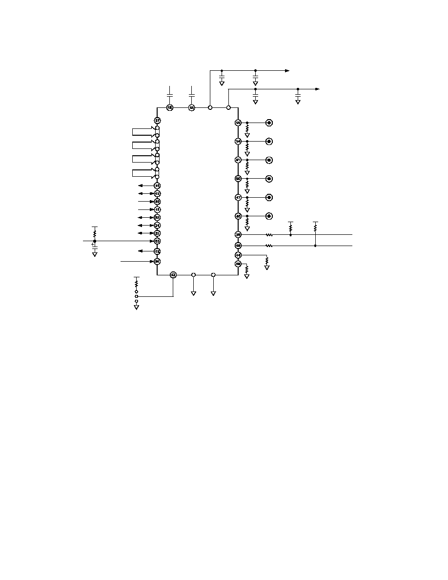
ADV7192
46
REV. A
5V (V
AA
)
COMP2
300
5k
5V (V
AA
)
5k
MPU BUS
0.1 F
5V (V
AA
)
4.7k
5V (V
AA
)
POWER SUPPLY DECOUPLING
FOR EACH POWER SUPPLY GROUP
10nF
AGND
ALSB
HSYNC
VSYNC
BLANK
RESET
CLKIN
R
SET1
SDATA
SCL
DAC A
V
AA
V
REF
5V (V
AA
)
SCRESET/RTC/TR
ADV7192
UNUSED
INPUTS
SHOULD BE
GROUNDED
DAC B
100
5V (V
AA
)
TTXREQ
0.1 F
COMP1
VSO/TTX/CLAMP
PAL_NTSC
DAC C
DAC D
DAC E
DAC F
R
SET2
27MHz CLOCK
(SAME CLOCK AS
USED BY MPEG2
DECODER)
CSO_HSO
4.7k
4.7 F
6.3V
V
DD
53,
48, 38
300
300
300
300
5V (V
AA
)
100
1.2k
1.2k
DGND
52, 49,
35
80, 69, 43,
33, 22
79, 68,
34, 21
10nF
0.1 F
5V (V
AA
)
0.1 F
300
Cb0 Cb9
Cr0 Cr9
Y0/P8 Y7/P15
Y8 Y9
P7 P0
Figure 78. Recommended Analog Circuit Layout
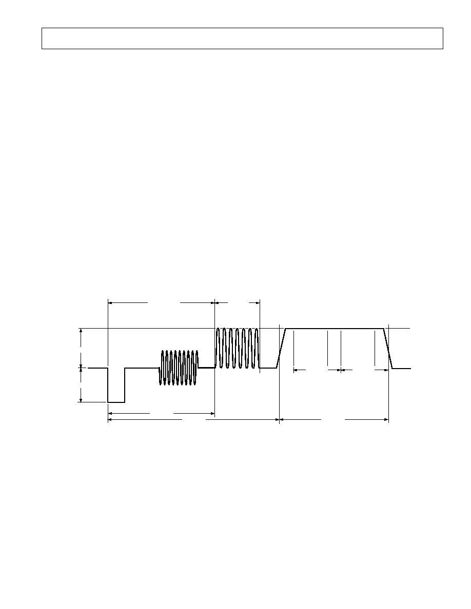
ADV7192
47
REV. A
APPENDIX 2
CLOSED CAPTIONING
The ADV7192 supports closed captioning conforming to the
standard television synchronizing waveform for color transmission.
Closed captioning is transmitted during the blanked active line
time of Line 21 of the odd fields and Line 284 of even fields.
Closed captioning consists of a seven-cycle sinusoidal burst that
is frequency and phase locked to the caption data. After the clock
run-in signal, the blanking level is held for two data bits and is
followed by a Logic Level 1 start bit. Sixteen bits of data follow
the start bit. These consist of two eight-bit bytes, seven data
bits, and one odd parity bit. The data for these bytes is stored
in Closed Captioning Data Registers 0 and 1.
The ADV7192 also supports the extended closed captioning
operation which is active during even fields and is encoded on
Scan Line 284. The data for this operation is stored in Closed
Captioning Extended Data Registers 0 and 1.
All clock run-in signals and timing to support Closed Captioning
on Lines 21 and 284 are generated automatically by the ADV7192
All pixels inputs are ignored during Lines 21 and 284 if closed
captioning is enabled.
FCC Code of Federal Regulations (CFR) 47 Section 15.119
and EIA608 describe the closed captioning information for Lines
21 and 284.
The ADV7192 uses a single buffering method. This means that
the closed captioning buffer is only one byte deep, therefore, there
will be no frame delay in outputting the closed captioning data
unlike other two byte deep buffering systems. The data must
be loaded one line before (Line 20 or Line 283) it is outputted
on Line 21 and Line 284. A typical implementation of this method
is to use
VSYNC to interrupt a microprocessor, which in turn will
load the new data (two bytes) every field. If no new data is required
for transmission, 0s must be inserted in both data registers, this
is called NULLING. It is also important to load control codes all
of which are double bytes on Line 21 or a TV will not recognize
them. If there is a message like Hello World which has an odd number
of characters, it is important to pad it out to even in order to get
end of caption 2-byte control code to land in the same field.
12.91 s
S
T
A
R
T
P
A
R
I
T
Y
P
A
R
I
T
Y
D0D6
D0D6
10.003 s
33.764 s
50 IRE
40 IRE
FREQUENCY = F
SC
= 3.579545MHz
AMPLITUDE = 40 IRE
REFERENCE COLOR BURST
(9 CYCLES)
7 CYCLES
OF 0.5035 MHz
(CLOCK RUN-IN)
10.5 0.25 s
TWO 7-BIT + PARITY
ASCII CHARACTERS
(DATA)
27.382 s
BYTE 0
BYTE 1
Figure 79. Closed Captioning Waveform (NTSC)
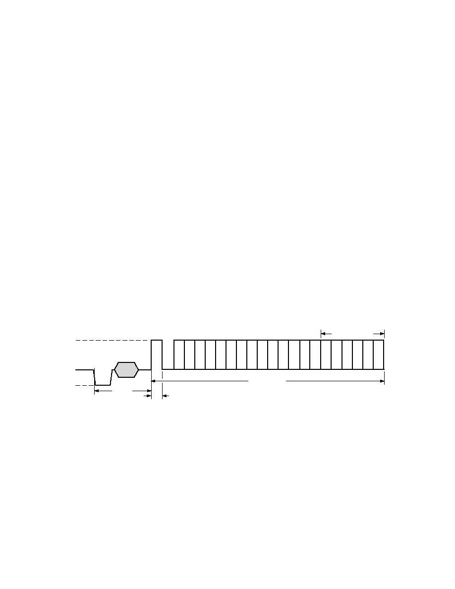
ADV7192
48
REV. A
APPENDIX 3
COPY GENERATION MANAGEMENT SYSTEM (CGMS)
The ADV7192 supports Copy Generation Management System
(CGMS) conforming to the standard. CGMS data is transmitted
on Line 20 of the odd fields and Line 283 of even fields. Bits
C/W05 and C/W06 control whether or not CGMS data is outputed
on ODD and EVEN fields. CGMS data can only be transmitted
when the ADV7192 is configured in NTSC mode. The CGMS
data is 20 bits long, the function of each of these bits is as shown
below. The CGMS data is preceded by a reference pulse of
the same amplitude and duration as a CGMS bit, see Figure 79.
These bits are outputed from the configuration registers in the
following order: C/W00 = C16, C/W01 = C17, C/W02 = C18,
C/W03 = C19, C/W10 = C8, C/W11 = C9, C/W12 = C10,
C/W13 = C11, C/W14 = C12, C/W15 = C13, C/W16 = C14,
C/W17 = C15, C/W20 = C0, C/W21 = C1, C/W22 = C2,
C/W23 = C3, C/W24 = C4, C/W25 = C5, C/W26 = C6,
C/W27 = C7. If the bit C/W04 is set to a Logic 1, the last six
bits C19C14 which comprise the 6-bit CRC check sequence
are calculated automatically on the ADV7192 based on the
lower 14 bits (C0C13) of the data in the data registers and
output with the remaining 14-bits to form the complete 20-bits
of the CGMS data. The calculation of the CRC sequence is
based on the polynomial X
6
+ X + 1 with a preset value of
111111. If C/W04 is set to a Logic 0 then all 20-bits (C0C19)
are output directly from the CGMS registers (no CRC calcu-
lated, must be calculated by the user).
Function of CGMS Bits
Word 0 6 Bits
Word 1 4 Bits
Word 2 6 Bits
CRC 6 Bits
CRC Polynomial = X
6
+ X + 1 (Preset to
111111)
WORD 0
1
0
B1
Aspect Ratio
16:9
4:3
B2
Display Format
Letterbox
Normal
B3
Undefined
WORD 0
B4, B5, B6
Identification Information About Video and
Other Signals (e.g., Audio)
WORD 1
B7, B8, B9,
Identification Signal Incidental to Word 0
B10
WORD 2
B11, B12,
Identification Signal and Information
B13, B14
Incidental to Word 0
CRC SEQUENCE
49.1 s
0.5 s
11.2 s
2.235 s
20ns
REF
C0
C1
C2
C3
C4
C5
C6
C7
C8
C9 C10 C11 C12 C13 C14 C15 C16 C17 C18 C19
100 IRE
70 IRE
0 IRE
40 IRE
Figure 80. CGMS Waveform Diagram
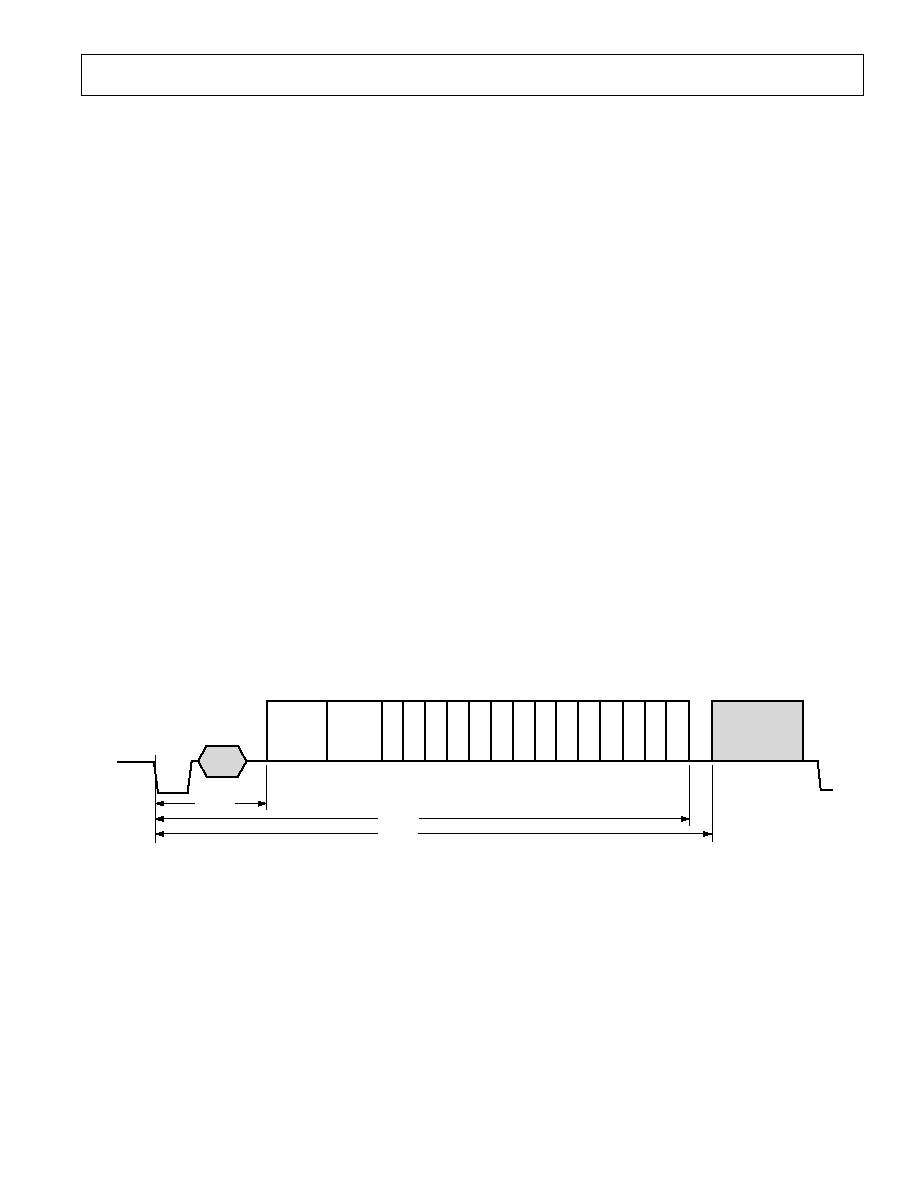
ADV7192
49
REV. A
APPENDIX 4
WIDE SCREEN SIGNALING
The ADV7192 supports Wide Screen Signaling (WSS) conforming
to the standard. WSS data is transmitted on Line 23. WSS data
can only be transmitted when the ADV7192 is configured in PAL
mode. The WSS data is 14-bits long, the function of each of these
bits is as shown below. The WSS data is preceded by a run-in
sequence and a Start Code, see Figure 80. The bits are output
from the configuration registers in the following order: C/W20 = W0,
C/W21 = W1, C/W22 = W2, C/W23 = W3, C/W24 = W4,
C/W25 = W5, C/W26 = W6, C/W27 = W7, C/W10 = W8,
C/W11 = W9, C/W12 = W10, C/W13 = W11, C/W14 = W12,
C/W15 = W13. If the bit C/W07 is set to a Logic 1, it enables
the WSS data to be transmitted on Line 23. The latter portion of
Line 23 (42.5
µs from the falling edge of HSYNC) is available for
the insertion of video.
Function of CGMS Bits
Bit 0Bit 2
Aspect Ratio/Format/Position
Bit 3
Is Odd Parity Check of Bit 0Bit 2
Aspect
Format
Position
B0, B1,
B2,
B3
Ratio
Format
Position
0
0
0
1
4:3
Full Format
Nonapplicable
1
0
0
0
14:9
Letterbox
Center
0
1
0
0
14:9
Letterbox
Top
1
1
0
1
16:9
Letterbox
Center
0
0
1
0
16:9
Letterbox
Top
1
0
1
1
>16:9
Letterbox
Center
0
1
1
1
14:9
Full Format
Center
1
1
1
0
16:9
Nonapplicable
Nonapplicable
B4
0
Camera Mode
1
Film Mode
B5
0
Standard Coding
1
Motion Adaptive Color Plus
B6
0
No Helper
1
Modulated Helper
B7
RESERVED
B9
B10
0
0
No Open Subtitles
1
0
Subtitles in Active Image Area
0
1
Subtitles Out of Active Image Area
1
1
RESERVED
B11
0
No Surround Sound Information
1
Surround Sound Mode
B12 RESERVED
B13 RESERVED
W0
W1 W2
W3 W4
W5
W6 W7
W8 W9 W10 W11 W12 W13
500mV
RUN-IN
SEQUENCE
START
CODE
ACTIVE
VIDEO
38.4 s
42.5 s
11.0 s
Figure 81. WSS Waveform Diagram
ADV7192
50
REV. A
Time, t
PD
,
is the time needed by the ADV7192 to interpolate
input data on TTX and insert it onto the CVBS or Y outputs,
such that it appears t
SYNTTXOUT
= 10.2
µs after the leading edge
of the horizontal signal. Time TTX
DEL
is the pipeline delay time
by the source that is gated by the TTXREQ signal in order to
deliver TTX data.
With the programmability that is offered with TTXREQ signal
on the Rising/Falling edges, the TTX data is always inserted at
the correct position of 10.2
µs after the leading edge of Horizontal
Sync pulse, thus this enables a source interface with variable
pipeline delays.
The width of the TTXREQ signal must always be maintained
such that it allows the insertion of 360 (in order to comply with
the Teletext Standard PAL-WST) teletext bits at a text data rate
of 6.9375 Mbits/s, this is achieved by setting TC03TC00 to 0.
The insertion window is not open if the Teletext Enable bit
(MR33) is set to 0.
APPENDIX 5
TELETEXT INSERTION
Teletext Protocol
The relationship between the TTX bit clock (6.9375 MHz) and
the system CLOCK (27 MHz) for 50 Hz is given as follows:
(27 MHz/4) = 6.75 MHz
(6.9375
× 10
6
/6.75
× 10
6
= 1.027777
Thus 37 TTX bits correspond to 144 clocks (27 MHz), each bit
has a width of almost four clock cycles. The ADV7192 uses an
internal sequencer and variable phase interpolation filter to mini-
mize the phase jitter and thus generate a bandlimited signal
which can be output on the CVBS and Y outputs.
At the TTX input the bit duration scheme repeats after every
37 TTX bits or 144 clock cycles. The protocol requires that
TTX Bits 10, 19, 28, 37 are carried by three clock cycles, all
other bits by four clock cycles. After 37 TTX bits, the next bits
with three clock cycles are Bits 47, 56, 65, and 74. This scheme
holds for all following cycles of 37 TTX bits, until all 360 TTX
bits are completed. All teletext lines are implemented in the
same way. Individual control of teletext lines are controlled
by Teletext Setup Registers.
ADDRESS & DATA
RUN-IN CLOCK
TELETEXT VBI LINE
45 BYTES (360 BITS) PAL
Figure 82. Teletext VBI Line
PROGRAMMABLE PULSE EDGES
t
PD
t
PD
CVBS/Y
HSYNC
TTXREQ
TTX
DATA
t
SYNTTXOUT
= 10.2 s
t
PD
= PIPELINE DELAY THROUGH ADV7192
TTX
DEL
= TTXREQ TO TTX (PROGRAMMABLE RANGE = 4 BITS [015 CLOCK CYCLES])
t
SYNTTXOUT
10.2 s
TTX
DEL
TTX
ST
Figure 83. Teletext Functionality Diagram
ADV7192
51
REV. A
APPENDIX 6
OPTIONAL OUTPUT FILTER
If an output filter is required for the CVBS, Y, UV, Chroma and
RGB outputs of the ADV7192, the following filter in Figure 84
can be used in 2
× Oversampling Mode. In 4× Oversampling
Mode the filter in Figure 86 is recommended. The plot of the fil-
ter characteristics are shown in Figures 85 and 87. An output filter
22 H
68pF
22 H
FILTER I/P
FILTER O/P
22pF
56pF
6.8 H
600
600
Figure 84. Output Filter for 2
× Oversampling Mode
100k
60
50
0
100M
70
MAGNITUDE dB
FREQUENCY Hz
1.0M
10M
40
30
20
10
Figure 85. Output Filter Plot for 2
× Oversampling Filter
is not required if the outputs of the ADV7192 are connected to
most analog monitors or TVs, however, if the output signals are
applied to a system where sampling is used, (e.g., Digital TVs)
then a filter is required to prevent aliasing.
10 H
68pF
22 H
FILTER I/P
FILTER O/P
27pF
600
600
Figure 86. Output Filter for 4
× Oversampling Mode
100k
63
49
42
100M
70
MAGNITUDE dB
FREQUENCY Hz
1.0M
10M
56
35
28
21
14
7
0
Figure 87. Output Filter Plot for 4
× Oversampling Filter
27.0
40.5
54.0
13.5
6.75
FREQUENCY MHz
2 FILTER
REQUIREMENTS
4 FILTER
REQUIREMENTS
0
30
dB
Figure 88. Output Filter Requirements in 4
× Oversampling Mode
ADV7192
52
REV. A
APPENDIX 7
DAC BUFFERING
External buffering is needed on the ADV7192 DAC outputs.
The configuration in Figure 89 is recommended.
When calculating absolute output full-scale current and voltage
use the following equations:
V
OUT
= I
OUT
× R
LOAD
I
OUT
= (V
REF
× K)/R
SET
K = 4.2146 constant, V
REF
= 1.235 V
ADV7192
V
REF
PIXEL
PORT
V
AA
OUTPUT
BUFFER
DAC A
CVBS
CHROMA
G
LUMA
B
R
1.2k
R
SET1
DAC B
DAC C
DAC D
DAC E
DAC F
DIGITAL
CORE
1.2k
R
SET2
OUTPUT
BUFFER
OUTPUT
BUFFER
OUTPUT
BUFFER
OUTPUT
BUFFER
OUTPUT
BUFFER
Figure 89. Output DAC Buffering Configuration
OUTPUT TO
TV MONITOR
INPUT/
OPTIONAL
FILTER O/P
+V
CC
AD8051
V
CC
1
5
4
3
2
Figure 90. Recommended DAC Output Buffer Using an
Op Amp

ADV7192
53
REV. A
APPENDIX 8
RECOMMENDED REGISTER VALUES
The ADV7192 registers can be set depending on the user standard required. The following examples give the various register formats
for several video standards.
NTSC (F
SC
= 3.5795454 MHz)
Address
Data
00Hex
Mode Register 0
10Hex
01Hex
Mode Register 1
3FHex
02Hex
Mode Register 2
62Hex
03Hex
Mode Register 3
00Hex
04Hex
Mode Register 4
00Hex
05Hex
Mode Register 5
00Hex
06Hex
Mode Register 6
00Hex
07Hex
Mode Register 7
00Hex
08Hex
Mode Register 8
04Hex
09Hex
Mode Register 9
00Hex
0AHex
Timing Register 0
08Hex
0BHex
Timing Register 1
00Hex
0CHex
Subcarrier Frequency Register 0
16Hex
0DHex
Subcarrier Frequency Register 1
7CHex
0EHex
Subcarrier Frequency Register 2
F0Hex
0FHex
Subcarrier Frequency Register 3
21Hex
10Hex
Subcarrier Phase Register
00Hex
11Hex
Closed Captioning Ext Register 0
00Hex
12Hex
Closed Captioning Ext Register 1
00Hex
13Hex
Closed Captioning Register 0
00Hex
14Hex
Closed Captioning Register 1
00Hex
15Hex
Pedestal Control Register 0
00Hex
16Hex
Pedestal Control Register 1
00Hex
17Hex
Pedestal Control Register 2
00Hex
18Hex
Pedestal Control Register 3
00Hex
19Hex
CGMS_WSS Reg 0
00Hex
1AHex
CGMS_WSS Reg 1
00Hex
1BHex
CGMS_WSS Reg 2
00Hex
1CHex
Teletext Control Register
00Hex
1DHex
Contrast Control Register
00Hex
1EHex
Color Control Register 1
00Hex
1FHex
Color Control Register 2
00Hex
20Hex
Hue Control Register
00Hex
21Hex
Brightness Control Register
00Hex
22Hex
Sharpness Response Register
00Hex
23Hex
DNR 0
44Hex
24Hex
DNR 1
20Hex
25Hex
DNR 2
00Hex
35Hex
Output Clock Register
70Hex
PAL B, D, G, H, I (F
SC
= 4.43361875 MHz)
Address
Data
00Hex
Mode Register 0
11Hex
01Hex
Mode Register 1
3FHex
02Hex
Mode Register 2
62Hex
03Hex
Mode Register 3
00Hex
04Hex
Mode Register 4
00Hex
05Hex
Mode Register 5
00Hex
06Hex
Mode Register 6
00Hex
07Hex
Mode Register 7
00Hex
08Hex
Mode Register 8
04Hex
09Hex
Mode Register 9
00Hex
0AHex
Timing Register 0
08Hex
0BHex
Timing Register 1
00Hex
0CHex
Subcarrier Frequency Register 0
CBHex
0DHex
Subcarrier Frequency Register 1
8AHex
0EHex
Subcarrier Frequency Register 2
09Hex
0FHex
Subcarrier Frequency Register 3
2AHex
10Hex
Subcarrier Phase Register
00Hex
11Hex
Closed Captioning Ext Register 0
00Hex
12Hex
Closed Captioning Ext Register 1
00Hex
13Hex
Closed Captioning Register 0
00Hex
14Hex
Closed Captioning Register 1
00Hex
15Hex
Pedestal Control Register 0
00Hex
16Hex
Pedestal Control Register 1
00Hex
17Hex
Pedestal Control Register 2
00Hex
18Hex
Pedestal Control Register 3
00Hex
19Hex
CGMS_WSS Reg 0
00Hex
1AHex
CGMS_WSS Reg 1
00Hex
1BHex
CGMS_WSS Reg 2
00Hex
1CHex
Teletext Control Register
00Hex
1DHex
Contrast Control Register
00Hex
1EHex
Color Control Register 1
00Hex
1FHex
Color Control Register 2
00Hex
20Hex
Hue Control Register
00Hex
21Hex
Brightness Control Register
00Hex
22Hex
Sharpness Response Register
00Hex
23Hex
DNR0
44Hex
24Hex
DNR1
20Hex
25Hex
DNR2
00Hex
35Hex
Output Clock Register
70Hex

ADV7192
54
REV. A
PAL N (F
SC
= 4.43361875 MHz)
Address
Data
00Hex
Mode Register 0
13Hex
01Hex
Mode Register 1
3FHex
02Hex
Mode Register 2
62Hex
03Hex
Mode Register 3
00Hex
04Hex
Mode Register 4
00Hex
05Hex
Mode Register 5
00Hex
06Hex
Mode Register 6
00Hex
07Hex
Mode Register 7
00Hex
08Hex
Mode Register 8
04Hex
09Hex
Mode Register 9
00Hex
0AHex
Timing Register 0
08Hex
0BHex
Timing Register 1
00Hex
0CHex
Subcarrier Frequency Register 0
CBHex
0DHex
Subcarrier Frequency Register 1
8AHex
0EHex
Subcarrier Frequency Register 2
09Hex
0FHex
Subcarrier Frequency Register 3
2AHex
10Hex
Subcarrier Phase Register
00Hex
11Hex
Closed Captioning Ext Register 0
00Hex
12Hex
Closed Captioning Ext Register 1
00Hex
13Hex
Closed Captioning Register 0
00Hex
4Hex
Closed Captioning Register 1
00Hex
15Hex
Pedestal Control Register 0
00Hex
16Hex
Pedestal Control Register 1
00Hex
17Hex
Pedestal Control Register 2
00Hex
18Hex
Pedestal Control Register 3
00Hex
19Hex
CGMS_WSS Reg 0
00Hex
1AHex
CGMS_WSS Reg 1
00Hex
1BHex
CGMS_WSS Reg 2
00Hex
1CHex
Teletext Control Register
00Hex
DHex
Contrast Control Register
00Hex
1EHex
Color Control Register 1
00Hex
1FHex
Color Control Register 2
00Hex
20Hex
Hue Control Register
00Hex
21Hex
Brightness Control Register
00Hex
22Hex
Sharpness Response Register
00Hex
23Hex
DNR 0
44Hex
24Hex
DNR 1
20Hex
25Hex
DNR 2
00Hex
35Hex
Output Clock Register
70Hex
PAL 60 (F
SC
= 4.43361875 MHz)
Address
Data
00Hex
Mode Register 0
12Hex
01Hex
Mode Register 1
3FHex
02Hex
Mode Register 2
62Hex
03Hex
Mode Register 3
00Hex
04Hex
Mode Register 4
00Hex
05Hex
Mode Register 5
00Hex
06Hex
Mode Register 6
00Hex
07Hex
Mode Register 7
00Hex
08Hex
Mode Register 8
04Hex
09Hex
Mode Register 9
00Hex
0AHex
Timing Register 0
08Hex
0BHex
Timing Register 1
00Hex
0CHex
Subcarrier Frequency Register 0
CBHex
0DHex
Subcarrier Frequency Register 1
8AHex
0EHex
Subcarrier Frequency Register 2
09Hex
0FHex
Subcarrier Frequency Register 3
2AHex
10Hex
Subcarrier Phase Register
00Hex
11Hex
Closed Captioning Ext Register 0
00Hex
12Hex
Closed Captioning Ext Register 1
00Hex
13Hex
Closed Captioning Register 0
00Hex
14Hex
Closed Captioning Register 1
00Hex
15Hex
Pedestal Control Register 0
00Hex
16Hex
Pedestal Control Register 1
00Hex
17Hex
Pedestal Control Register 2
00Hex
18Hex
Pedestal Control Register 3
00Hex
19Hex
CGMS_WSS Reg 0
00Hex
1AHex
CGMS_WSS Reg 1
00Hex
1BHex
CGMS_WSS Reg 2
00Hex
1CHex
Teletext Control Register
00Hex
1DHex
Contrast Control Register
00Hex
1EHex
Color Control Register 1
00Hex
1FHex
Color Control Register 2
00Hex
20Hex
Hue Control Register
00Hex
21Hex
Brightness Control Register
00Hex
22Hex
Sharpness Response Register
00Hex
23Hex
DNR 0
44Hex
24Hex
DNR 1
20Hex
25Hex
DNR 2
00Hex
35Hex
Output Clock Register
70Hex

ADV7192
55
REV. A
PAL M (F
SC
= 3.57561149 MHz)
Address
Data
00Hex
Mode Register 0
12Hex
01Hex
Mode Register 1
3FHex
02Hex
Mode Register 2
62Hex
03Hex
Mode Register 3
00Hex
04Hex
Mode Register 4
00Hex
05Hex
Mode Register 5
00Hex
06Hex
Mode Register 6
00Hex
07Hex
Mode Register 7
00Hex
08Hex
Mode Register 8
04Hex
09Hex
Mode Register 9
00Hex
0AHex
Timing Register 0
08Hex
0BHex
Timing Register 1
00Hex
0CHex
Subcarrier Frequency Register 0
A3Hex
0DHex
Subcarrier Frequency Register 1
EFHex
EHex
Subcarrier Frequency Register 2
E6Hex
0FHex
Subcarrier Frequency Register 3
21Hex
10Hex
Subcarrier Phase Register
00Hex
11Hex
Closed Captioning Ext Register 0
00Hex
12Hex
Closed Captioning Ext Register 1
00Hex
Address
Data
13Hex
Closed Captioning Register 0
00Hex
14Hex
Closed Captioning Register 1
00Hex
15Hex
Pedestal Control Register 0
00Hex
16Hex
Pedestal Control Register 1
00Hex
17Hex
Pedestal Control Register 2
00Hex
18Hex
Pedestal Control Register 3
00Hex
19Hex
CGMS_WSS Reg 0
00Hex
1AHex
CGMS_WSS Reg 1
00Hex
1BHex
CGMS_WSS Reg 2
00Hex
1CHex
Teletext Control Register
00Hex
1DHex
Contrast Control Register
00Hex
1EHex
Color Control Register 1
00Hex
1FHex
Color Control Register 2
00Hex
20Hex
Hue Control Register
00Hex
21Hex
Brightness Control Register
00Hex
22Hex
Sharpness Response Register
00Hex
23Hex
DNR 0
44Hex
24Hex
DNR 1
20Hex
25Hex
DNR 2
00Hex
35Hex
Output Clock Register
70Hex

ADV7192
56
REV. A
POWER-ON RESET REG VALUES
(PAL_NTSC = 0, NTSC Selected)
Address
Data
00Hex
Mode Register 0
00Hex
01Hex
Mode Register 1
07Hex
02Hex
Mode Register 2
08Hex
03Hex
Mode Register 3
00Hex
04Hex
Mode Register 4
00Hex
05Hex
Mode Register 5
00Hex
06Hex
Mode Register 6
00Hex
07Hex
Mode Register 7
00Hex
08Hex
Mode Register 8
00Hex
09Hex
Mode Register 9
00Hex
0AHex
Timing Register 0
08Hex
0BHex
Timing Register 1
00Hex
0CHex
Subcarrier Frequency Register 0
16Hex
0DHex
Subcarrier Frequency Register 1
7CHex
0EHex
Subcarrier Frequency Register 2
F0Hex
0FHex
Subcarrier Frequency Register 3
21Hex
10Hex
Subcarrier Phase Register
00Hex
11Hex
Closed Captioning Ext Register 0
00Hex
12Hex
Closed Captioning Ext Register 1
00Hex
13Hex
Closed Captioning Register 0
00Hex
14Hex
Closed Captioning Register 1
00Hex
15Hex
Pedestal Control Register 0
00Hex
16Hex
Pedestal Control Register 1
00Hex
17Hex
Pedestal Control Register 2
00Hex
18Hex
Pedestal Control Register 3
00Hex
19Hex
CGMS_WSS Reg 0
00Hex
1AHex
CGMS_WSS Reg 1
00Hex
1BHex
CGMS_WSS Reg 2
00Hex
1CHex
Teletext Control Register
00Hex
1DHex
Contrast Control Register
00Hex
1EHex
Color Control Register 1
00Hex
1FHex
Color Control Register 2
00Hex
20Hex
Hue Control Register
00Hex
21Hex
Brightness Control Register
00Hex
22Hex
Sharpness Response Register
00Hex
23Hex
DNR 0
00Hex
24Hex
DNR 1
00Hex
25Hex
DNR 2
00Hex
26Hex
Gamma 0
xxHex
27Hex
Gamma 1
xxHex
28Hex
Gamma 2
xxHex
29Hex
Gamma 3
xxHex
2AHex
Gamma 4
xxHex
2BHex
Gamma 5
xxHex
2CHex
Gamma 6
xxHex
2DHex
Gamma 7
xxHex
2EHex
Gamma 8
xxHex
2FHex
Gamma 9
xxHex
30Hex
Gamma 10
xxHex
31Hex
Gamma 11
xxHex
32Hex
Gamma 12
xxHex
33Hex
Gamma 13
xxHex
34Hex
Brightness Detect Register
xxHex
35Hex
Output Clock Register
72Hex
POWER-ON RESET REG VALUES
(PAL_NTSC = 1, PAL Selected)
Address
Data
00Hex
Mode Register 0
01Hex
01Hex
Mode Register 1
07Hex
02Hex
Mode Register 2
08Hex
03Hex
Mode Register 3
00Hex
04Hex
Mode Register 4
00Hex
05Hex
Mode Register 5
00Hex
06Hex
Mode Register 6
00Hex
07Hex
Mode Register 7
00Hex
08Hex
Mode Register 8
00Hex
09Hex
Mode Register 9
00Hex
0AHex
Timing Register 0
08Hex
0BHex
Timing Register 1
00Hex
0CHex
Subcarrier Frequency Register 0
CBHex
0DHex
Subcarrier Frequency Register 1
8AHex
0EHex
Subcarrier Frequency Register 2
09Hex
0FHex
Subcarrier Frequency Register 3
2AHex
10Hex
Subcarrier Phase Register
00Hex
11Hex
Closed Captioning Ext Register 0
00Hex
12Hex
Closed Captioning Ext Register 1
00Hex
13Hex
Closed Captioning Register 0
00Hex
14Hex
Closed Captioning Register 1
00Hex
15Hex
Pedestal Control Register 0
00Hex
16Hex
Pedestal Control Register 1
00Hex
17Hex
Pedestal Control Register 2
00Hex
18Hex
Pedestal Control Register 3
00Hex
19Hex
CGMS_WSS Reg 0
00Hex
1AHex
CGMS_WSS Reg 1
00Hex
1BHex
CGMS_WSS Reg 2
00Hex
1CHex
Teletext Control Register
00Hex
1DHex
Contrast Control Register
00Hex
1EHex
Color Control Register 1
00Hex
1FHex
Color Control Register 2
00Hex
20Hex
Hue Control Register
00Hex
21Hex
Brightness Control Register
00Hex
22Hex
Sharpness Response Register
00Hex
23Hex
DNR 0
00Hex
24Hex
DNR 1
00Hex
25Hex
DNR 2
00Hex
26Hex
Gamma 0
xxHex
27Hex
Gamma 1
xxHex
28Hex
Gamma 2
xxHex
29Hex
Gamma 3
xxHex
2AHex
Gamma 4
xxHex
2BHex
Gamma 5
xxHex
2CHex
Gamma 6
xxHex
2DHex
Gamma 7
xxHex
2EHex
Gamma 8
xxHex
2FHex
Gamma 9
xxHex
30Hex
Gamma 10
xxHex
31Hex
Gamma 11
xxHex
32Hex
Gamma 12
xxHex
33Hex
Gamma 13
xxHex
34Hex
Brightness Detect Register
xxHex
35Hex
Output Clock Register
72Hex
POWER-ON RESET REGISTER VALUES
ADV7192
57
REV. A
APPENDIX 9
NTSC WAVEFORMS (WITH PEDESTAL)
130.8 IRE
100 IRE
7.5 IRE
0 IRE
40 IRE
PEAK COMPOSITE
REF WHITE
BLACK LEVEL
SYNC LEVEL
BLANK LEVEL
714.2mV
1268.1mV
1048.4mV
387.6mV
334.2mV
48.3mV
Figure 91. NTSC Composite Video Levels
100 IRE
7.5 IRE
0 IRE
40 IRE
REF WHITE
BLACK LEVEL
SYNC LEVEL
BLANK LEVEL
714.2mV
1048.4mV
387.6mV
334.2mV
48.3mV
Figure 92. NTSC Luma Video Levels
650mV
335.2mV
963.8mV
0mV
PEAK CHROMA
BLANK/BLACK LEVEL
286mV (p-p)
629.7mV (p-p)
PEAK CHROMA
Figure 93. NTSC Chroma Video Levels
100 IRE
7.5 IRE
0 IRE
40 IRE
REF WHITE
BLACK LEVEL
SYNC LEVEL
BLANK LEVEL
720.8mV
1052.2mV
387.5mV
331.4mV
45.9mV
Figure 94. NTSC RGB Video Levels
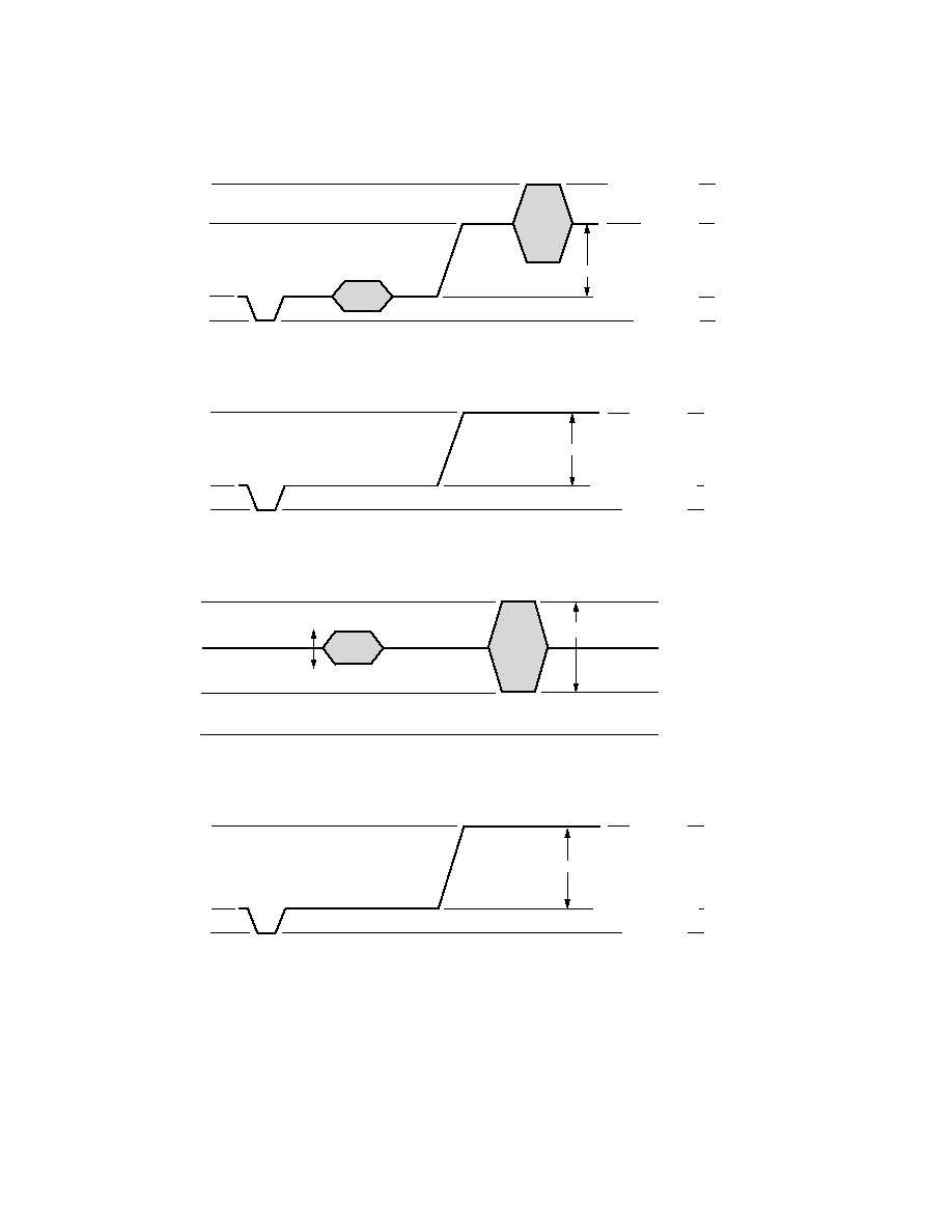
ADV7192
58
REV. A
NTSC WAVEFORMS (WITHOUT PEDESTAL)
130.8 IRE
100 IRE
0 IRE
40 IRE
PEAK COMPOSITE
REF WHITE
SYNC LEVEL
BLANK/BLACK LEVEL
714.2mV
1289.8mV
1052.2mV
338mV
52.1mV
Figure 95. NTSC Composite Video Levels
100 IRE
0 IRE
40 IRE
REF WHITE
SYNC LEVEL
BLANK/BLACK LEVEL
714.2mV
1052.2mV
338mV
52.1mV
Figure 96. NTSC Luma Video Levels
650mV
283mV
978mV
0mV
PEAK CHROMA
BLANK/BLACK LEVEL
307mV (p-p)
PEAK CHROMA
694.9mV (p-p)
Figure 97. NTSC Chroma Video Levels
100 IRE
0 IRE
40 IRE
REF WHITE
SYNC LEVEL
BLANK/BLACK LEVEL
715.7mV
1052.2mV
336.5mV
51mV
Figure 98. NTSC RGB Video Levels
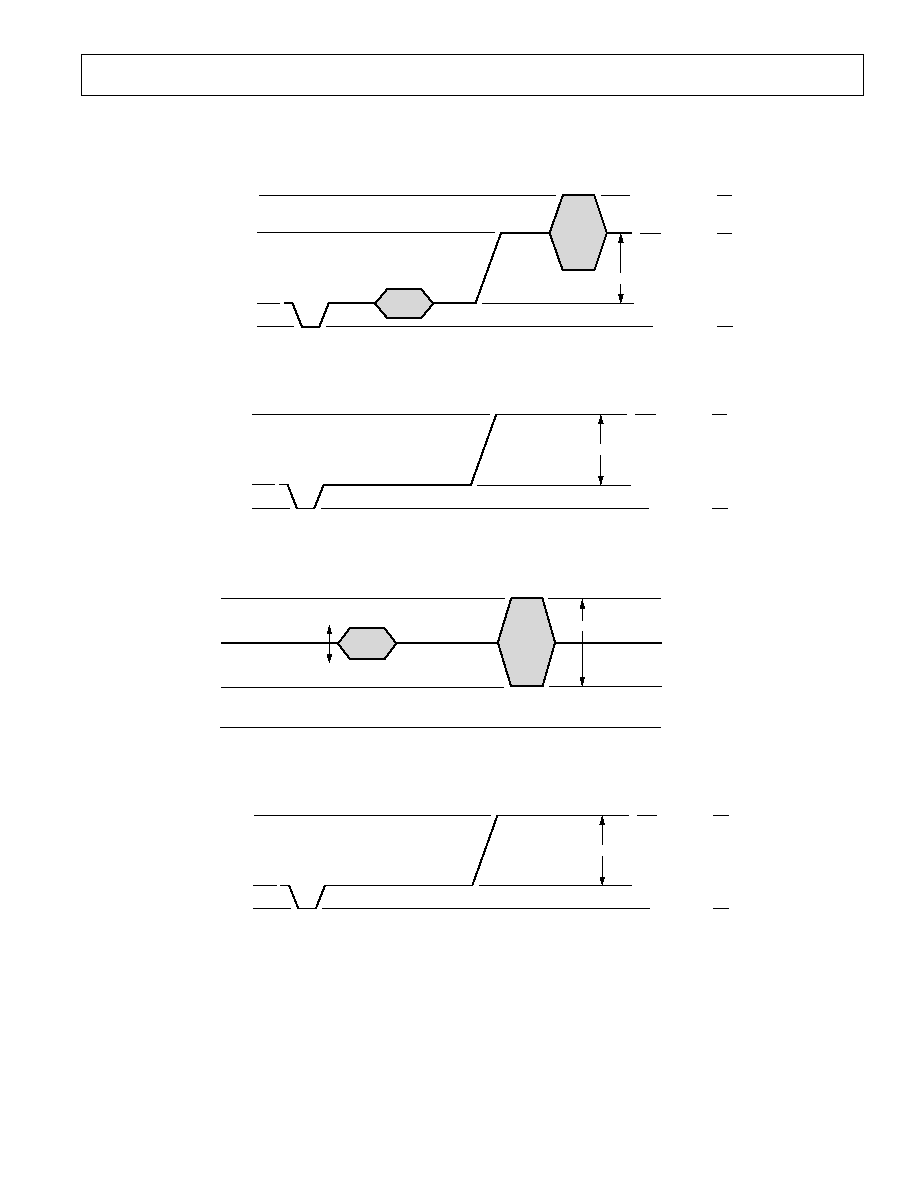
ADV7192
59
REV. A
PAL WAVEFORMS
1284.2mV
1047.1mV
350.7mV
50.8mV
PEAK COMPOSITE
REF WHITE
SYNC LEVEL
BLANK/BLACK LEVEL
696.4mV
Figure 99. PAL Composite Video Levels
1047mV
350.7mV
50.8mV
REF WHITE
SYNC LEVEL
BLANK/BLACK LEVEL
696.4mV
Figure 100. PAL Luma Video Levels
650mV
318mV
990mV
0mV
PEAK CHROMA
BLANK/BLACK LEVEL
300mV (p-p)
672mV (p-p)
PEAK CHROMA
Figure 101. PAL Chroma Video Levels
1050.2mV
351.8mV
51mV
REF WHITE
SYNC LEVEL
BLANK/BLACK LEVEL
698.4mV
Figure 102. PAL RGB Video Levels
ADV7192
60
REV. A
VIDEO MEASUREMENT PLOTS
GRAY
YELLOW
CYAN
GREEN
MAGENTA
RED
BLUE
BLACK
0
50
100
LUMINANCE LEVEL (IRE)
99.6
69.0
55.9
48.1
36.3
28.3
15.7
7.7
GRAY
YELLOW
CYAN
GREEN
MAGENTA
RED
BLUE
BLACK
0.0
62.1
87.6
81.8
81.8
87.8
62.1
0.0
CHROMINANCE LEVEL (IRE)
0
50
100
GRAY
YELLOW
CYAN
GREEN
MAGENTA
RED
BLUE
BLACK
400
200
0
167.3
283.8
240.9
60.80
103.6
347.1
CHROMINANCE PHASE (DEGREE)
AVERAGE 32
32
COLOR BAR (NTSC)
FIELD = 1
LINE = 21
WFM
FCC COLOR BAR
Figure 103. NTSC Color Bar Measurement
GRAY
YELLOW
CYAN
GREEN
MAGENTA
RED
BLUE
BLACK
0
500
1000
LUMINANCE LEVEL (mV)
695.7
464.8
366.6
305.7
217.3
156.4
61.2
0.4
GRAY
YELLOW
CYAN
GREEN
MAGENTA
RED
BLUE
BLACK
0
500
1000
0.0
474.4
669.1
623.5
624.7
669.6
475.2
0.0
CHROMINANCE LEVEL (mV)
GRAY
YELLOW
CYAN
GREEN
MAGENTA
RED
BLUE
BLACK
400
200
0
100
300
166.7
283.3
240.4
60.4
103.2
346.7
CHROMINANCE PHASE (DEGREE)
AVERAGE 32
32
COLOR BAR (PAL)
FIELD = 1
LINE = 21
WFM
FCC COLOR BAR
Figure 104. PAL Color Bar Measurement
ADV7192
61
REV. A
DG DP (NTSC) WFM
FIELD = 1, LINE = 21
MOD 5 STEP
1
st
2.5
1.5
0.5
0.5
1.5
2.5
2
nd
3
rd
4
th
5
th
6
th
0.00
0.21
0.02
0.07
0.27
0.08
DIIFFERENTIAL GAIN (PERCENT)
MIN = 0.00, MAX = 0.27, p-p/MAX = 0.27
1
st
2.5
1.5
0.5
0.5
1.5
2.5
2
nd
3
rd
4
th
5
th
6
th
0.00
0.10
0.12
0.15
0.13
0.10
DIFFERENTIAL PHASE (DEGREE)
MIN = 0.00, MAX = 0.20, p-p = 0.20
AVERAGE 32
32
Figure 105. NTSC DG DP Measurement
89
91
93
95
97
99
101
103
105
107
109
111
1
st
2
nd
3
rd
4
th
5
th
99.9
99.9
99.6
100.0
99.9
AVERAGE 32
32
LUMINANCE NONLINEARITY (NTSC)
WFM
FIELD = 2, LINE = 77
LUMINANCE NONLINEARITY (PERCENT)
MOD 5 STEP
p-p = 0.4
Figure 106. NTSC Luminance Nonlinearity
1
st
2.5
1.5
0.5
0.5
1.5
2.5
2
nd
3
rd
4
th
5
th
6
th
0.00
0.09
0.13
0.16
0.12
0.14
DIFFERENTIAL PHASE (DEGREE)
MIN = 0.00, MAX = 0.16, p-p = 0.16
1
st
2.5
1.5
0.5
0.5
1.5
2.5
2
nd
3
rd
4
th
5
th
6
th
0.00
0.30
0.15
0.24
0.32
0.26
DIIFFERENTIAL GAIN (PERCENT)
MIN = 0.00, MAX = 0.32, p-p/MAX = 0.32
DG DP (PAL) WFM
LINE = 570
MOD 5 STEP
AVERAGE 32
32
Figure 107. PAL DG DP Measurement
91
93
95
97
99
101
103
105
107
109
111
113
1
st
2
nd
3
rd
4
th
5
th
99.6
99.9
100.0
99.6
99.9
AVERAGE 32
32
LUMINANCE NONLINEARITY (PAL)
WFM
LINE = 570
LUMINANCE NONLINEARITY (PERCENT)
p-p = 0.8
MOD 5 STEP
Figure 108. PAL Luminance Nonlinearity
ADV7192
62
REV. A
20IRE
10
10
0
40IRE
80IRE
0.5
0.0
0.3
CHROMINANCE AMPLITUDE ERROR (PERCENT) REF = 40IRE PACKET
20IRE
5
5
0
40IRE
80IRE
0.0
0.0
0.0
CHROMINANCE PHASE ERROR (DEGREE) REF = 40IRE PACKET
20IRE
0.1
0.2
0.1
40IRE
80IRE
0.0
0.1
0.1
0.0
0.2
AVERAGE 32
32
CHROMINANCE LUMINANCE INTERMODULATION (PERCENT OF 714 mV)
CHROMINANCE NONLINEARITY(NTSC) WFM NTSC7 COMBINATION
FIELD = 2, LINE = 217
Figure 109. NTSC Chrominance Nonlinearity
95
90
85
80
75
70
65
60
95
90
85
80
75
70
65
60
PM NOISE
82.7dB RMS
AM NOISE
86.5dB RMS
(0dB = 714mV p-p WITH AGC FOR 100% CHROMINANCE LEVEL)
dB RMS
dB RMS
CHROMINANCE AM/PM (NTSC)
WFM
RED FIELD
FIELD = 2, LINE = 217
BANDWIDTH 10kHz TO 100kHz
Figure 110. NTSC Chrominance AM/PM
CHROMINANCE NONLINEARITY(PAL) WFM MOD 3 STEP
LINE = 572
140mV
10
10
0
420mV
700mV
0.6
0.0
0.4
CHROMINANCE AMPLITUDE ERROR (PERCENT) REF = 420mV PACKET
140mV
5
0
420mV
700mV
0.3
0.0
0.3
CHROMINANCE PHASE ERROR (DEGREE) REF = 420mV PACKET
140mV
0.2
420mV
700mV
0.0
0.0
0.1
0.0
0.2
AVERAGE 32
32
CHROMINANCE LUMINANCE INTERMODULATION (PERCENT OF 700mV)
Figure 111. PAL Chrominance Nonlinearity
95
90
85
80
75
70
65
60
95
90
85
80
75
70
65
60
PM NOISE
82.7dB RMS
AM NOISE
84.2dB RMS
(0dB = 700mV p-p WITH AGC FOR 100% CHROMINANCE LEVEL)
dB RMS
dB RMS
CHROMINANCE AM/PM (PAL)
WFM APPROPRIATE
LINE = 572
BANDWIDTH 10kHz TO 100kHz
Figure 112. PAL Chrominance AM/PM
ADV7192
63
REV. A
100
80
60
40
20
0
20
NOISE SPECTRUM (NTSC)
WFM
FIELD = 2, LINE = 223
AMPLITUDE (0dB = 714mV p-p)
1
2
3
4
5
6
MHz
BANDWIDTH 10kHz TO FULL
PEDESTAL
NOISE LEVEL = 79.7dB RMS
Figure 113. NTSC Noise Spectrum: Pedestal
100
90
80
50
40
20
0
NOISE SPECTRUM (NTSC)
WFM
FIELD = 2, LINE = 217
AMPLITUDE (0dB = 714mV p-p)
1
2
3
4
5
6
MHz
BANDWIDTH 100kHz TO FULL (TILT NULL)
70
60
30
10
RAMP
NOISE LEVEL = 63.1dB RMS
Figure 114. NTSC Noise Spectrum: Ramp
100
80
60
40
20
0
NOISE SPECTRUM (PAL)
WFM
LINE = 511
AMPLITUDE (0dB = 714mV p-p)
1
2
3
4
5
7
MHz
BANDWIDTH 10kHz TO FULL
6
PEDESTAL
NOISE LEVEL = 79.1dB RMS
Figure 115. PAL Noise Spectrum: Pedestal
100
90
80
50
40
20
0
NOISE SPECTRUM (PAL)
WFM
LINE = 572
AMPLITUDE (0dB = 700mV pp)
1
2
3
4
5
7
MHz
BANDWIDTH 100kHz TO FULL (TILT NULL)
70
60
30
10
6
NOISE LEVEL = 62.3dB RMS
RAMP
Figure 116. PAL Noise Spectrum: Ramp
ADV7192
64
REV. A
BETACAM LEVEL
0mV
171mV
334mV
505mV
0mV
171mV
334mV
505mV
WHITE
YELLOW
CYAN
GREEN
MAGENTA
RED
BLUE
BLACK
Figure 117. NTSC 100% Color Bars No Pedestal U Levels
BETACAM LEVEL
0mV
158mV
309mV
467mV
0mV
158mV
309mV
467mV
WHITE
YELLOW
CYAN
GREEN
MAGENTA
RED
BLUE
BLACK
Figure 118. NTSC 100% Color Bars with Pedestal U Levels
SMPTE LEVEL
0mV
118mV
232mV
350mV
0mV
118mV
232mV
350mV
WHITE
YELLOW
CYAN
GREEN
MAGENTA
RED
BLUE
BLACK
Figure 119. PAL 100% Color Bars U Levels
UV WAVEFORMS
BETACAM LEVEL
0mV
82mV
423mV
505mV
0mV
82mV
505mV
423mV
WHITE
YELLOW
CYAN
GREEN
MAGENTA
RED
BLUE
BLACK
Figure 120. NTSC 100% Color Bars No Pedestal V Levels
BETACAM LEVEL
0mV
76mV
391mV
467mV
0mV
76mV
467mV
391mV
WHITE
YELLOW
CYAN
GREEN
MAGENTA
RED
BLUE
BLACK
Figure 121. NTSC 100% Color Bars with Pedestal V
SMPTE LEVEL
0mV
57mV
293mV
350mV
0mV
57mV
350mV
293mV
WHITE
YELLOW
CYAN
GREEN
MAGENTA
RED
BLUE
BLACK
Figure 122. PAL 100% Color Bars V Levels
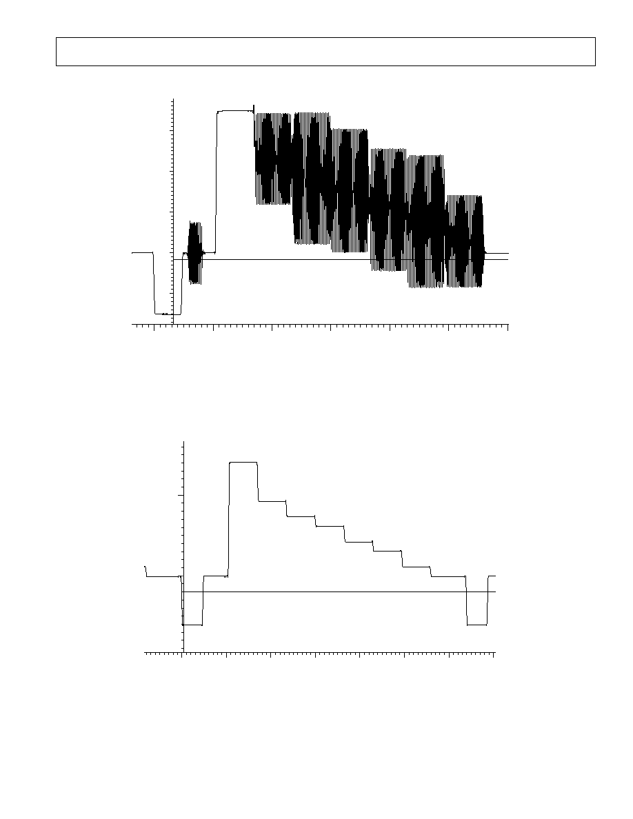
ADV7192
65
REV. A
0.6
0.4
0.2
0.0
0.2
L608
0.0
10.0
20.0
30.0
40.0
50.0
60.0
MICROSECONDS
NOISE REDUCTION: 0.00 dB
APL = 39.1%
PRECISION MODE OFF
SOUND-IN-SYNC OFF
625 LINE PAL
NO FILTERING
SYNCHRONOUS
SYNC = SOURCE
SLOW CLAMP TO 0.00 V AT 6.72 s
FRAMES SELECTED: 1 2 3 4
VOLTS
Figure 123. 100/0/75/0 PAL Color Bars
MICROSECONDS
APL NEEDS SYNC = SOURCE!
PRECISION MODE OFF
SOUND-IN-SYNC OFF
625 LINE PAL
NO FILTERING
SYNCHRONOUS
SYNC = A
SLOW CLAMP TO 0.00 V AT 6.72 s
FRAMES SELECTED: 1
0.5
0.0
L575
0.0
10.0
20.0
30.0
40.0
50.0
60.0
70.0
VOLTS
NO BRUCH SIGNAL
Figure 124. 100/0/75/0 PAL Color Bars Luminance
OUTPUT WAVEFORMS
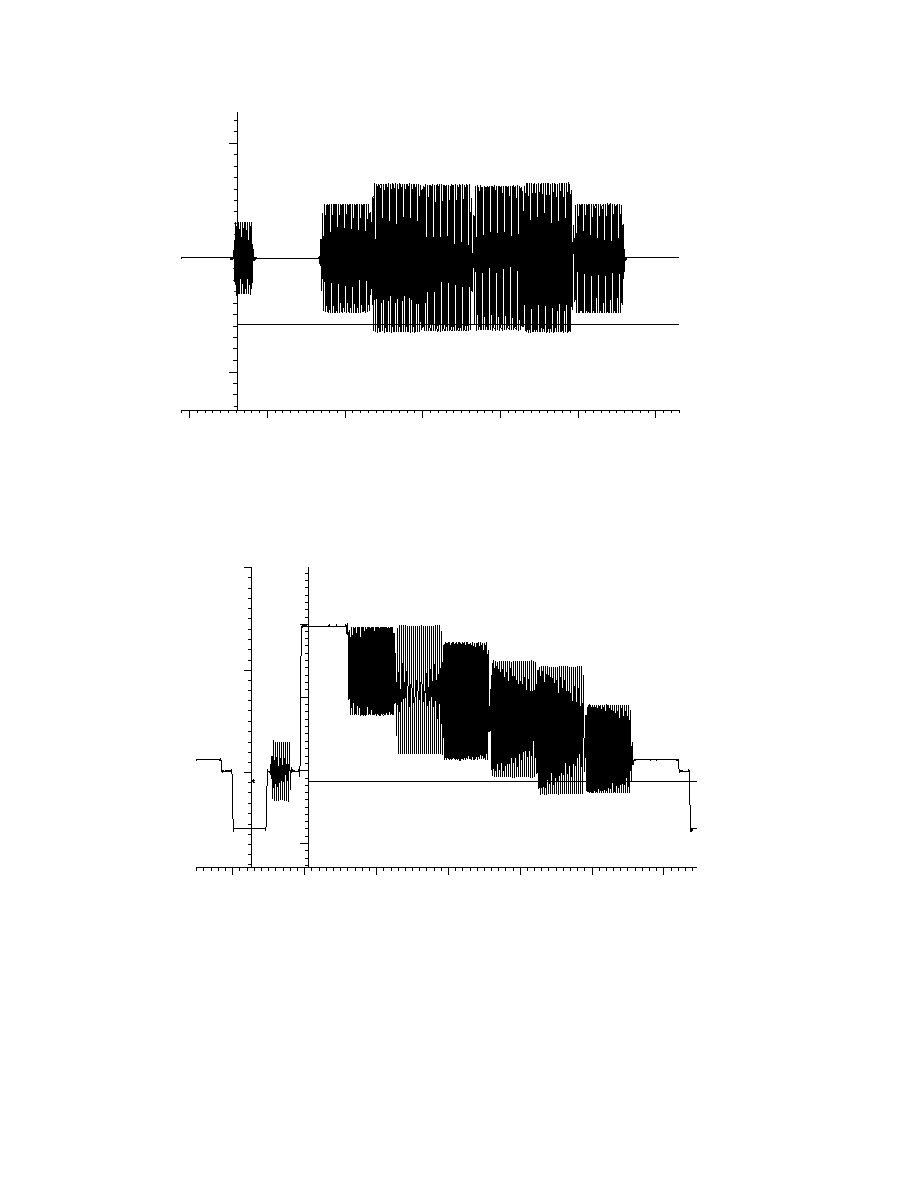
ADV7192
66
REV. A
APL NEEDS SYNC = SOURCE!
PRECISION MODE OFF
SOUND-IN-SYNC OFF
625 LINE PAL
NO FILTERING
SYNCHRONOUS
SYNC = A
SLOW CLAMP TO 0.00 V AT 6.72 s
FRAMES SELECTED: 1
0.5
0.0
0.5
10.0
30.0
40.0
50.0
60.0
20.0
MICROSECONDS
L575
VOLTS
NO BRUCH SIGNAL
Figure 125. 100/0/75/0 PAL Color Bars Chrominance
APL = 44.6%
PRECISION MODE OFF
525 LINE NTSC
NO FILTERING
SYNCHRONOUS
SYNC = A
SLOW CLAMP TO 0.00 V AT 6.72 s
FRAMES SELECTED: 1 2
MICROSECONDS
0.5
0.0
50.0
50.0
100.0
IRE:FLT
VOLTS
F1
L76
0.0
10.0
20.0
30.0
40.0
50.0
60.0
0.0
Figure 126. 100/7.5/75/7.5 NTSC Color Bars
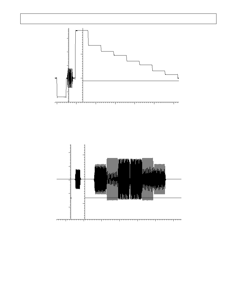
ADV7192
67
REV. A
NOISE REDUCTION: 15.05dB
APL = 44.7%
PRECISION MODE OFF
525 LINE NTSC
NO FILTERING
SYNCHRONOUS
SYNC = SOURCE
SLOW CLAMP TO 0.00 V AT 6.72 s
FRAMES SELECTED: 1 2
MICROSECONDS
10.0
20.0
30.0
40.0
50.0
60.0
0.6
0.4
0.2
0.0
0.2
50.0
0.0
IRE:FLT
VOLTS
F2
L238
100.0
Figure 127. 100/7.5/75/7.5 NTSC Color Bars Luminance
NOISE REDUCTION: 15.05dB
APL NEEDS SYNC = SOURCE!
PRECISION MODE OFF
525 LINE NTSC
NO FILTERING
SYNCHRONOUS
SYNC = B
SLOW CLAMP TO 0.00 V AT 6.72 s
FRAMES SELECTED: 1 2
MICROSECONDS
0.0
10.0
20.0
30.0
40.0
50.0
60.0
0.4
0.2
0.0
0.2
0.4
VOLTS
50.0
50.0
F1
L76
IRE:FLT
Figure 128. 100/7.5/75/7.5 NTSC Color Bars Chrominance
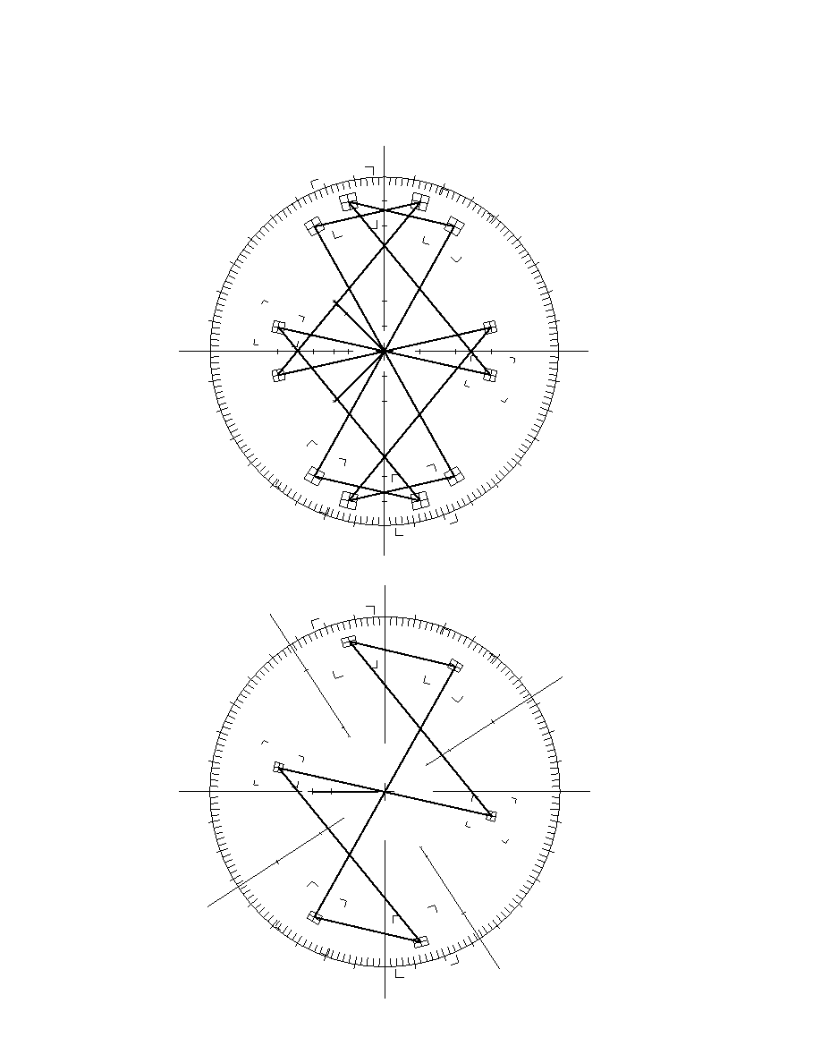
ADV7192
68
REV. A
APPENDIX 10
VECTOR PLOTS
APL = 39.6%
SOUND IN SYNC OFF
V
U
YI
yl
G
r
m
g
Cy
M
g
cy
g
R
75%
100%
b
B
SYSTEM LINE L608
ANGLE (DEG) 0.0
GAIN 1.000 0.000dB
625 LINE PAL
BURST FROM SOURCE
DISPLAY +V AND V
Figure 129. PAL Vector Plot
APL = 45.1%
SETUP 7.5%
R-Y
B-Y
YI
G
Cy
M
g
cy
I
R
75%
100%
b
B
SYSTEM LINE L76F1
ANGLE (DEG) 0.0
GAIN 1.000 0.000dB
525 LINE NTSC
BURST FROM SOURCE
Q
Q
I
Figure 130. NTSC Vector Plot
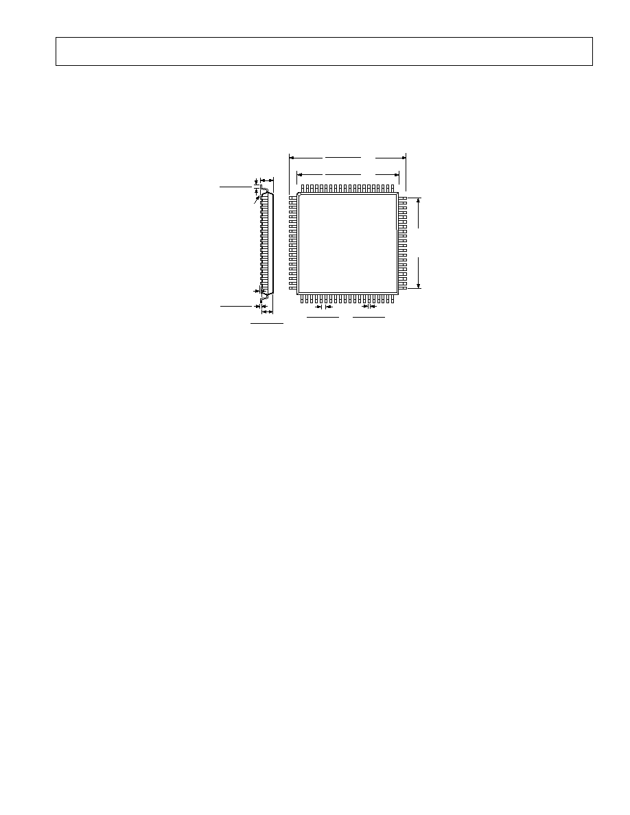
ADV7192
69
REV. A
OUTLINE DIMENSIONS
Dimensions shown in inches and (mm).
80-Lead LQFP
(ST-80)
TOP VIEW
(PINS DOWN)
1
20
21
41
40
60
61
80
0.640 (16.25)
0.620 (15.75)
SQ
0.553 (14.05)
0.549 (13.95)
SQ
0.014 (0.35)
0.010 (0.25)
0.029 (0.73)
0.022 (0.57)
0.486
(12.35)
TYP
SQ
0.063 (1.60)
MAX
0.030 (0.75)
0.020 (0.50)
SEATING
PLANE
0.006 (0.15)
0.002 (0.05)
0.004 (0.10)
MAX
0.057 (1.45)
0.053 (1.35)
C00229012/00 (rev. A)
PRINTED IN U.S.A.