Äîêóìåíòàöèÿ è îïèñàíèÿ www.docs.chipfind.ru
REV. A
a
Information furnished by Analog Devices is believed to be accurate and
reliable. However, no responsibility is assumed by Analog Devices for its
use, nor for any infringements of patents or other rights of third parties that
may result from its use. No license is granted by implication or otherwise
under any patent or patent rights of Analog Devices.
ADV7302A/ADV7303A
Multiformat SD, Progressive Scan/HDTV
Video Encoder with Six 11-Bit DACs
One Technology Way, P.O. Box 9106, Norwood, MA 02062-9106, U.S.A.
Tel: 781/329-4700
www.analog.com
Fax: 781/326-8703
© Analog Devices, Inc., 2002
*ADV7302A Only
FEATURES
High Definition Input Formats
YCrCb Compliant to SMPTE293M (525 p),
ITU-R.BT1358 (625 p), SMPTE274M (1080 i),
SMPTE296M (720 p), and Any Other High Definition
Standard Using Async Timing Mode
RGB in 3 8-Bit 4:4:4 Format
BTA T-1004 EDTV2 525 p Parallel
High Definition Output Formats (525 p/625 p/720 p/1080 i)
YPrPb Progressive Scan (EIA-770.1, EIA-770.2)
YPrPb HDTV (EIA 770.3)
RGB + H/V (HDTV 5-Wire Format)
CGMS-A (720 p/1080 i)
Macrovision Rev 1.0 (525 p/625 p)*
CGMS-A (525 p)
Standard Definition Input Formats
CCIR-656 4:2:2 8-Bit Parallel Input
CCIR-601 4:2:2 16-Bit Parallel Input
Standard Definition Output Formats
Composite NTSC M, N;
PAL M, N, B, D, G, H, I, PAL-60
SMPTE170M NTSC Compatible Composite Video
ITU-R.BT470 PAL Compatible Composite Video
S-Video (Y/C)
EuroScart RGB
Component YUV (Betacam, MII, SMPTE/EBU N10)
Macrovision Rev 7.1*
CGMS/WSS
Closed Captioning
GENERAL FEATURES
Simultaneous SD and HD Inputs and Outputs
Oversampling (108 MHz/148.5 MHz)
On-Board Voltage Reference
6 Precision Video 11-Bit DACs
2-Wire Serial MPU Interface
Dual I/O Supply 2.5 V/3.3 V Operation
Analog and Digital Supply 2.5 V
On-Board PLL
64-LQFP Package
Lead-Free Product
APPLICATIONS
DVD Players
SD/HD Display Devices
SD/HD Set-Top Boxes
SD/HDTV Studio Equipment
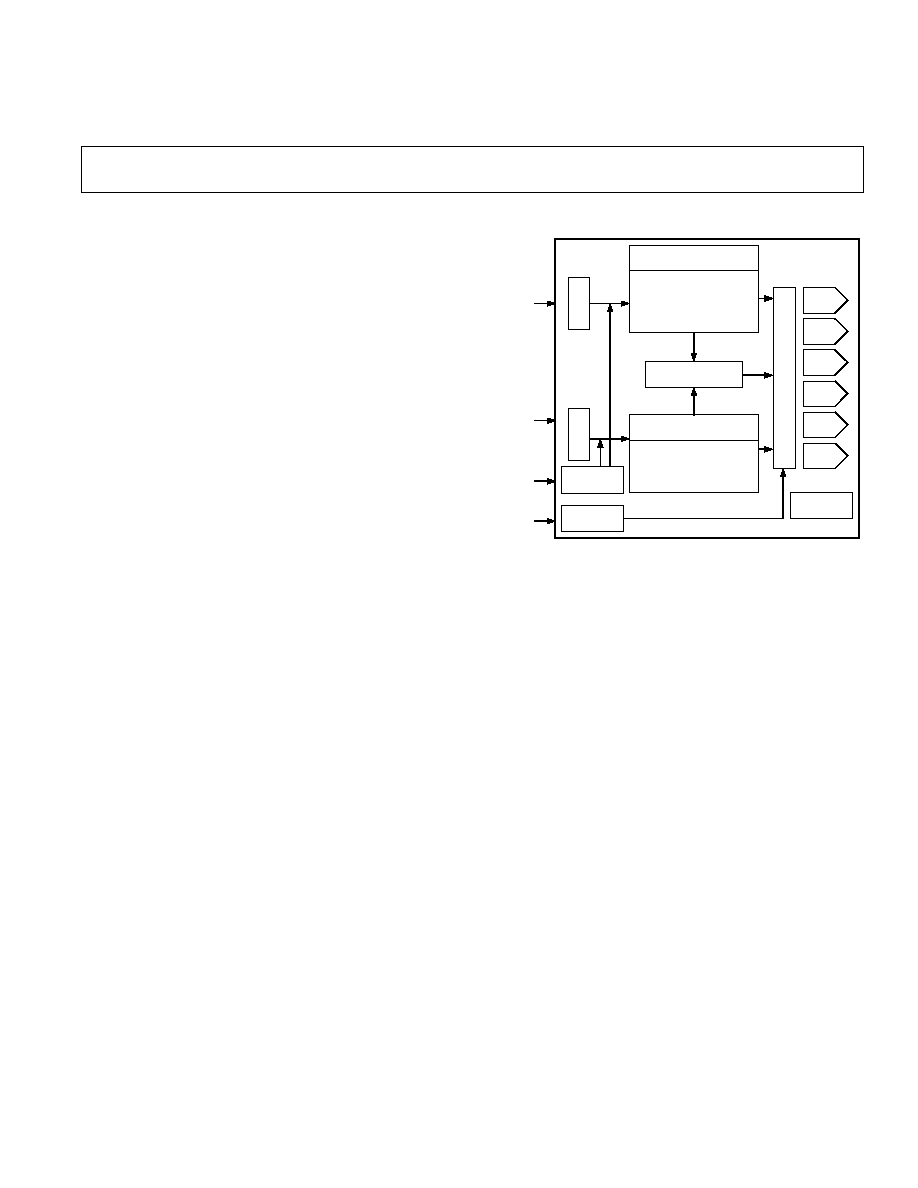
SIMPLIFIED FUNCTIONAL BLOCK DIAGRAM
S7S0
Y7Y0
C7C0
S_HSYNC
S_VSYNC
S_BLANK
P_HSYNC
P_VSYNC
P_BLANK
CLKIN_A
CLKIN_B
D
E
M
U
X
TIMING
GENERATOR
PLL
O
V
E
R
S
A
M
P
L
I
N
G
I
2
C
INTERFACE
D
E
M
U
X
STANDARD DEFINITION
CONTROL BLOCK
COLOR CONTROL
BRIGHTNESS
DNR
GAMMA
PROGRAMMABLE FILTERS
SD TEST PATTERN
HIGH DEFINITION
CONTROL BLOCK
HD TEST PATTERN
COLOR CONTROL
ADAPTIVE FILTER CTRL
SHARPNESS FILTER
PROGRAMMABLE
RGB MATRIX
11-BIT
DAC
11-BIT
DAC
11-BIT
DAC
11-BIT
DAC
11-BIT
DAC
11-BIT
DAC
ADV7302A/
ADV7303A
GENERAL DESCRIPTION
The ADV7302A/ADV7303A is a high speed, digital-to-analog
encoder on a single monolithic chip. It includes six high speed
video D/A converters with TTL compatible inputs.
The ADV7302A/ADV7303A has three separate 8-bit wide input
ports that accept data in high definition and/or standard defini-
tion video format. For all standards, external horizontal, vertical,
and blanking signals, or EAV/SAV timing codes, control the
insertion of appropriate synchronization signals into the digital
data stream and therefore the output signals.
REV. A
2
ADV7302A/ADV7303A
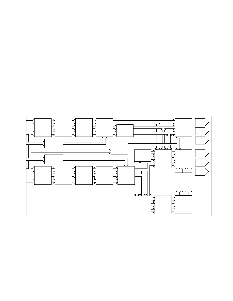
FSC
MODULATION
S_HSYNC
S_VSYNC
S_BLANK
CLKIN_A
P_HSYNC
P_VSYNC
P_BLANK
CLKIN_B
HD PIXEL
INPUT
SD PIXEL
INPUT
DE-
INTER-
LEAVE
Y
CB
CR
TEST
PATTERN
SHARPNESS
AND
ADAPTIVE
FILTER
CONTROL
Y COLOR
CR COLOR
CB COLOR
4:2:2
TO
4:4:4
TIMING
GENERATOR
TIMING
GENERATOR
DE-
INTER-
LEAVE
Y
CB
CR
TEST
PATTERN
DNR
GAMMA
COLOR
CONTROL
SYNC
INSER-
TION
CLOCK
CONTROL
AND PLL
2 OVER-
SAMPLING
UV SSAF
V
U
PS 4
HDTV 2
RGB
MATRIX
SD 8
LUMA
AND
CHROMA
FILTERS
CGMS
WSS
DAC
DAC
DAC
DAC
DAC
DAC
Figure 1. Functional Block Diagram
DETAILED FEATURES
High Definition Programmable Features (720 p/1080 i)
2 Oversampling (148.5 MHz)
Internal Test Pattern Generator (Color Hatch, Black
Bar, Flat Field/Frame)
Fully Programmable YCrCb to RGB Matrix
Gamma Correction
Programmable Adaptive Filter Control
Programmable Sharpness Filter Control
CGMS-A (720 p/1080 i)
High Definition Programmable Features (525 p/625 p)
4 Oversampling (108 MHz Output)
Internal Test Pattern Generator (Color Hatch, Black
Bar, Flat Frame)
Individual Y and PrPb Output Delay
Gamma Correction
Programmable Adaptive Filter Control
Fully Programmable YCrCb to RGB Matrix
Undershoot Limiter
TERMS USED IN THIS DATA SHEET
SD
Standard Definition Video, conforming to
ITU-R.BT601/ITU-R.BT656.
HD
High Definition Video, i.e., Progressive Scan or HDTV.
PS
Progressive Scan Video, conforming to SMPTE293M
or ITU-R.BT1358.
Macrovision Rev 1.0 (525 p/625 p)*
CGMS-A (525 p)
Standard Definition Programmable Features
8
Oversampling (108 MHz)
Internal Test Pattern Generator (Color Bars, Black Bar)
Controlled Edge Rates for Sync, Active Video
Individual Y and UV Output Delay
Gamma Correction
Digital Noise Reduction
Multiple Chroma and Luma Filters
Luma-SSAF
TM
Filter with Programmable Gain/
Attenuation
UV SSAF
Separate Pedestal Control on Component and
Composite/S-Video Outputs
VCR FF/RW Sync Mode
Macrovision Rev 7.1*
CGMS/WSS
Closed Captioning
SSAF is a trademark of Analog Devices, Inc.
*ADV7302A Only
HDTV
High Definition Television Video, conforming to
SMPTE274M or SMPTE296M.
YCrCb
SD or HD Component Digital Video
YPrPb
HD Component Analog Video
YUV
SD Component Analog Video

REV. A
3
ADV7302A/ADV7303ASPECIFICATIONS
Parameter
Min
Typ
Max
Unit
Test Conditions
STATIC PERFORMANCE
1
Resolution
11
Bits
Integral Nonlinearity
±1.0
LSB
V
AA
= 2.5 V
Differential Nonlinearity, +ve
2
0.125
LSB
V
AA
= 2.5 V
Differential Nonlinearity, ve
2
1.0
LSB
V
AA
= 2.5 V
DIGITAL OUTPUTS
Output Low Voltage, V
OL
0.4 [0.4]
3
V
I
SINK
= 3.2 mA
Output High Voltage, V
OH
2.4 [2.0]
3
V
I
SOURCE
= 400
µA
Three-State Leakage Current
±1.0
µA
V
IN
= 0.4 V, 2.4 V
Three-State Output Capacitance
2
pF
DIGITAL AND CONTROL INPUTS
Input High Voltage, V
IH
2
V
Input Low Voltage, V
IL
0.8
V
Input Leakage Current
1
µA
V
IN
= 2.4 V
Input Capacitance, C
IN
2
pF
ANALOG OUTPUTS
Full-Scale Output Current
8.2
8.7
9.2
mA
Output Current Range
8.2
8.7
9.2
mA
Full-Scale Output Current
4.1
4.35
4.6
mA
R
SET1, 2
= 1520
Output Current Range
4.1
4.35
4.6
mA
R
SET1, 2
= 1520
DAC to DAC Matching
2.0
%
Output Compliance Range, V
OC
0
1.0
1.4
V
Output Capacitance, C
OUT
7
pF
VOLTAGE REFERENCE
Reference Range, V
REF
1.15
1.235
1.3
V
POWER REQUIREMENTS
Normal Power Mode
I
DD
4
93
mA
SD Only [8 ]
52
mA
PS Only [4 ]
84
mA
HDTV Only [2 ]
90
110
mA
SD and PS
99
mA
SD [8 ] and HDTV
108
mA
SD and HDTV [2 ]
I
DD_IO
0.2
mA
I
AA
5, 6
70
75
mA
37
45
mA
R
SET1, 2
= 1520
Sleep Mode
I
DD
130
µA
I
AA
10
µA
I
DD_IO
110
µA
Power Supply Rejection Ratio
0.01
%/%
NOTES
1
Oversampling disabled. Static DAC performance will be improved with increased oversampling ratios.
2
DNL measures the deviation of the actual DAC o/p voltage step from the ideal. For +ve DNL, the actual step value lies above the ideal step value; for ve DNL, the
actual step values lie below the ideal step value.
3
Value in brackets for V
DD_IO
= 2.375 V to 2.750 V.
4
I
DD
or the circuit current is the continuous current required to drive the digital core without the I
PLL
.
5
I
AA
is the total current required to supply all DACs including the V
REF
circuitry and the PLL circuitry.
6
All DACs on.
Specifications subject to change without notice.
(V
AA
= V
DD
= 2.375 V2.625 V, V
DD_IO
= 2.375 V3.600 V, V
REF
= 1.235 V, R
SET
= 760 , R
LOAD
= 150 , T
MIN
to T
MAX
(0 C to 70 C), unless otherwise noted.)

REV. A
4
ADV7302A/ADV7303A
DYNAMIC SPECIFICATIONS
Parameter
Min
Typ
Max
Unit
Test Conditions
PROGRESSIVE SCAN MODE
Luma Bandwidth
12.5
MHz
Chroma Bandwidth
5.8
MHz
SNR
59
dB
Luma Ramp Unweighted
SNR
75
dB
Flat Field up to 5 MHz
SNR
70
dB
Flat Field Full Bandwidth
HDTV MODE
Luma Bandwidth
30
MHz
Chroma Bandwidth
13.75
MHz
SNR
59
dB
Luma Ramp Unweighted
SNR
75
dB
Flat Field up to 5 MHz
SNR
70
dB
Flat Field Full Bandwidth
STANDARD DEFINITION MODE
Hue Accuracy
0.2
Degrees
Color Saturation Accuracy
0.54
%
Chroma Nonlinear Gain
±0.4
%
Referenced to 40 IRE
Chroma Nonlinear Phase
±0.3
Degrees
Chroma/Luma Intermod
±0.05
%
Chroma/Luma Gain Ineq
±98
%
Chroma/Luma Delay Ineq
0.9
ns
Luminance Nonlinearity
±0.4
%
Chroma AM Noise
84
dB
Chroma PM Noise
74
dB
Differential Gain
0.6
%
NTSC
Differential Phase
1.4
Degrees
NTSC
SNR
59
dB
Luma Ramp
SNR
75
dB
Flat Field up to 5 MHz
SNR
70
dB
Flat Field Full Bandwidth
Specifications subject to change without notice.
(V
AA
= V
DD
= 2.375 V2.625 V, V
DD_IO
= 2.375 V3.600 V, V
REF
= 1.235 V, R
SET
= 760
,
R
LOAD
= 150
, T
MIN
to T
MAX
(0 C to 70 C), unless otherwise noted.)

REV. A
ADV7302A/ADV7303A
5
TIMING SPECIFICATIONS
Parameter
Min
Typ
Max
Unit
Test Conditions
MPU PORT
1
SCLOCK Frequency
0
400
kHz
SCLOCK High Pulsewidth, t
1
0.6
µs
SCLOCK Low Pulsewidth, t
2
1.3
µs
Hold Time (Start Condition), t
3
0.6
µs
First Clock Generated After
This Period
Setup Time (Start Condition), t
4
0.6
µs
Relevant for Repeated Start
Condition
Data Setup Time, t
5
100
ns
SDATA, SCLOCK Rise Time, t
6
300
ns
SDATA, SCLOCK Fall Time, t
7
300
ns
Setup Time (Stop Condition), t
8
0.6
µs
RESET Low Time
100
ns
ANALOG OUTPUTS
Analog Output Delay
2
8
ns
Output Skew
1
ns
CLOCK CONTROL AND PIXEL PORT
3
f
CLK
27
MHz
Progressive Scan Mode
f
CLK
81
MHz
HDTV Mode/Async Mode
Clock High Time, t
9
40
% 1 clkcycle
Clock Low Time, t
10
40
% 1 clkcycle
Data Setup Time, t
11
2.0
ns
Data Hold Time, t
12
1
2.0
ns
Output Access Time, t
13
14
ns
Output Hold Time, t
14
4.0
ns
Pipeline Delay
61
clkcycles
SD [2 ]
62.5
clkcycles
SD [8 ]
66.5
clkcycles
SD Component Filter [8 ]
33
clkcycles
PS [1 ], HD [1 ], Async
Timing Mode
43.5
clkcycles
PS [4 ]
36
clkcycles
HD [2 ]
NOTES
1
Guaranteed by characterization.
2
Output delay measured from the 50% point of the rising edge of CLOCK to the 50% point of DAC output full-scale transition.
3
Data: C[7:0]; S[7:0]; Y[7:0]
Control:
P_HSYNC; P_ VSYNC; P_BLANK; S_HSYNC; S_VSYNC; S_BLANK
Specifications subject to change without notice.
(V
AA
= V
DD
= 2.375 V2.625 V, V
DD_IO
= 2.375 V3.600 V, V
REF
= 1.235 V, R
SET
= 760
, R
LOAD
= 150
,
T
MIN
to T
MAX
(0 C to 70 C), unless otherwise noted.)
Document Outline