Äîêóìåíòàöèÿ è îïèñàíèÿ www.docs.chipfind.ru
Multiformat 11-Bit
HDTV Video Encoder
Preliminary Technical Data
ADV7322
Rev. PrA
Information furnished by Analog Devices is believed to be accurate and reliable.
However, no responsibility is assumed by Analog Devices for its use, nor for any
infringements of patents or other rights of third parties that may result from its use.
Specifications subject to change without notice. No license is granted by implication
or otherwise under any patent or patent rights of Analog Devices. Trademarks and
registered trademarks are the property of their respective owners.
One Technology Way, P.O. Box 9106, Norwood, MA 02062-9106, U.S.A.
Tel: 781.329.4700
www.analog.com
Fax: 781.326.8703
© 2004 Analog Devices, Inc. All rights reserved.
FEATURES
High definition input formats
16-, 24-bit (4:2:2, 4:4:4) parallel YCrCb
Fully compliant with
SMPTE 274M (1080i, 1080p @ 74.25 MHz)
SMPTE 296M (720p)
SMPTE 240M (1035i)
RGB in 3- × 8-bit 4:4:4 input format
HDTV RGB supported
RGB, RGBHV
Other high definition formats using async
timing mode
Enhanced definition input formats
8-, 16-, 24-bit (4:2:2, 4:4:4) parallel YCrCb
SMPTE 293M (525p)
BTA T-1004 EDTV2 (525p)
ITU-R BT.1358 (625p/525p)
ITU-R BT.1362 (625p/525p)
RGB in 3- × 8-bit 4:4:4 input format
Standard definition input formats
CCIR-656 4:2:2 8-bit or 16-bit parallel input
High definition output formats
YPrPb HDTV (EIA 770.3)
RGB, RGBHV
CGMS-A (720p/1080i)
Enhanced definition output formats
Macrovision Rev 1.2 (525p/625p)
CGMS-A (525p/625p)
YPrPb progressive scan (EIA-770.1, EIA-770.2)
RGB, RGBHV
Standard definition output formats
Composite NTSC M/N
Composite PAL M/N/B/D/G/H/I, PAL-60
SMPTE 170M NTSC-compatible composite video
ITU-R BT.470 PAL-compatible composite video
S-video (Y/C)
EuroScart RGB
Component YPrPb (Betacam, MII, SMPTE/EBU N10)
Macrovision Rev 7.1.L1
CGMS/WSS
Closed captioning
GENERAL FEATURES
Simultaneous SD/HD, PS/SD inputs and outputs
Oversampling up to 216 MHz
Programmable DAC gain control
Sync outputs in all modes
On-board voltage reference
Six 11-bit precision video DACs
2-wire serial I
2
C® interface, open-drain configuration
Dual I/O supply 2.5 V/3.3 V operation
Analog and digital supply 2.5 V
On-board PLL
64-lead LQFP package
Lead (Pb)-free product
APPLICATIONS
EVD players (enhanced versatile disk)
SD/PS DVD recorders/players
SD/progressive scan/HDTV display devices
SD/HDTV set top boxes
CLKIN_A
CLKIN_B
HSYNC
VSYNC
BLANK
Y7Y0
C7C0
S7S0
TIMING
GENERATOR
PLL
O
V
E
R
S
A
M
P
L
I
N
G
I
2
C
INTERFACE
D
E
M
U
X
STANDARD DEFINITION
CONTROL BLOCK
COLOR CONTROL
BRIGHTNESS
DNR
GAMMA
PROGRAMMABLE
FILTERS
SD TEST PATTERN
HIGH DEFINITION
CONTROL BLOCK
HD TEST PATTERN
COLOR CONTROL
ADAPTIVE FILTER CTRL
SHARPNESS FILTER
PROGRAMMABLE
RGB MATRIX
11-BIT
DAC
11-BIT
DAC
11-BIT
DAC
11-BIT
DAC
11-BIT
DAC
11-BIT
DAC
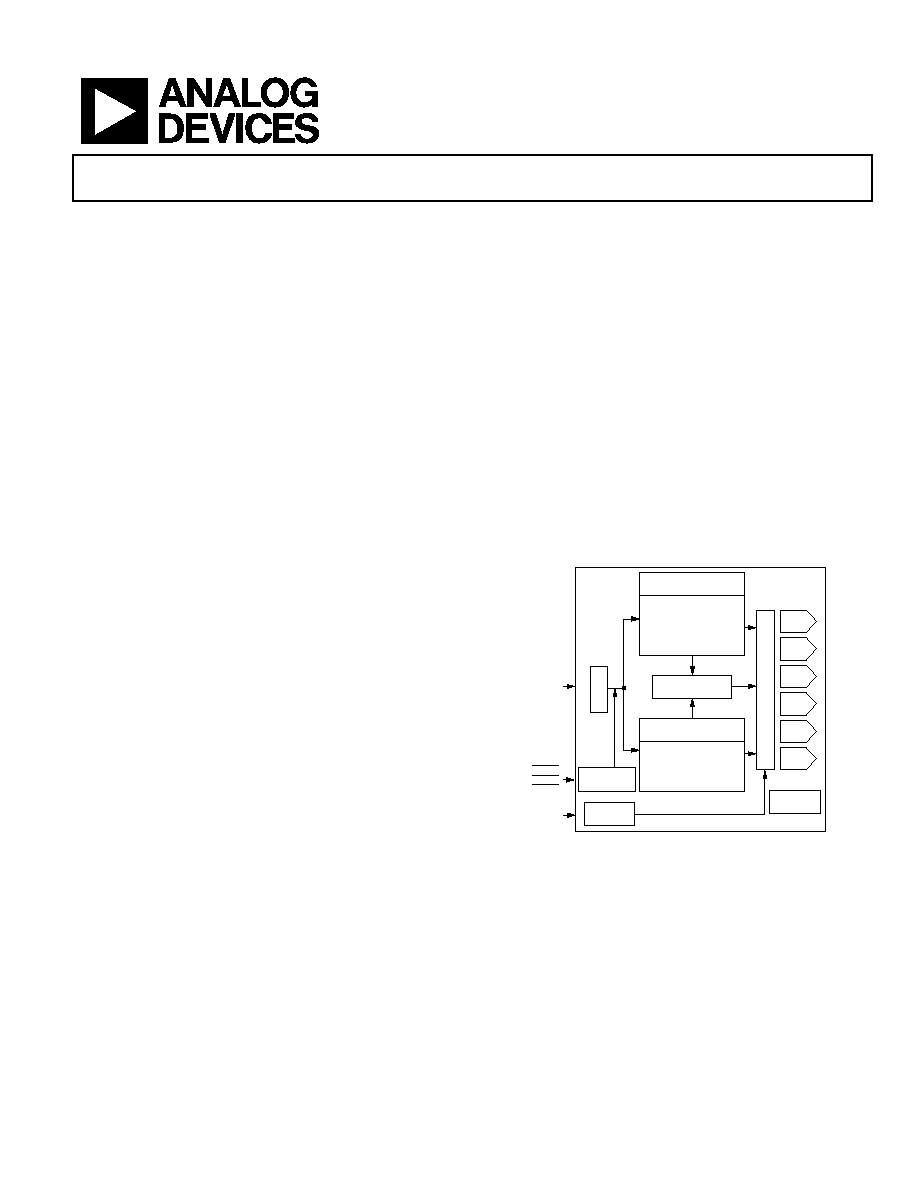
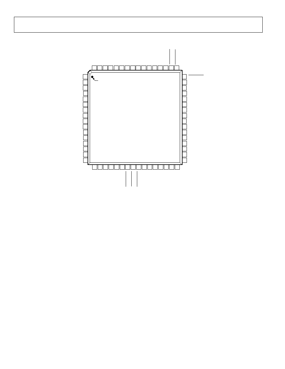
ADV7322
05067-001
Figure 1. Simplified Functional Block Diagram
GENERAL DESCRIPTION
The ADV®7322 is a high speed, digital-to-analog encoder on a
single monolithic chip. It includes six high speed video DACs
with TTL compatible inputs. It has separate 8-, 16-, 24-bit input
ports that accept data in high definition and/or standard
definition video format. For all standards, external horizontal,
vertical, and blanking signals or EAV/SAV timing codes control
the insertion of appropriate synchronization signals into the
digital data stream and therefore the output signal.

ADV7322
Preliminary Technical Data
Rev. PrA | Page 2 of 88
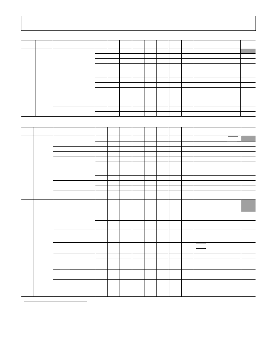
TABLE OF CONTENTS
Specifications..................................................................................... 6
Dynamic Specifications ................................................................... 7
Timing Specifications....................................................................... 8
Timing Diagrams.............................................................................. 9
Absolute Maximum Ratings.......................................................... 17
Thermal Characteristics ............................................................ 17
Pin Configuration and Function Descriptions........................... 18
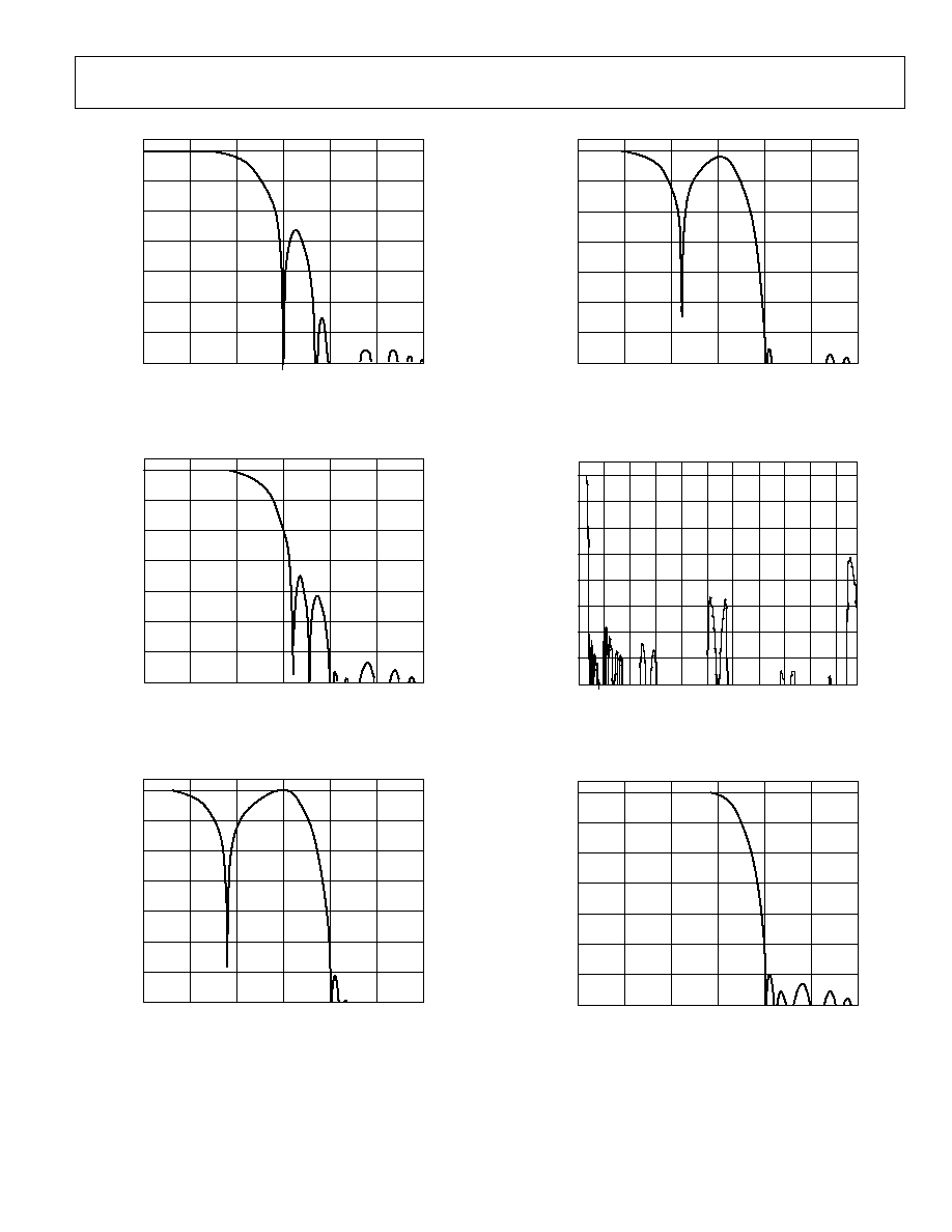
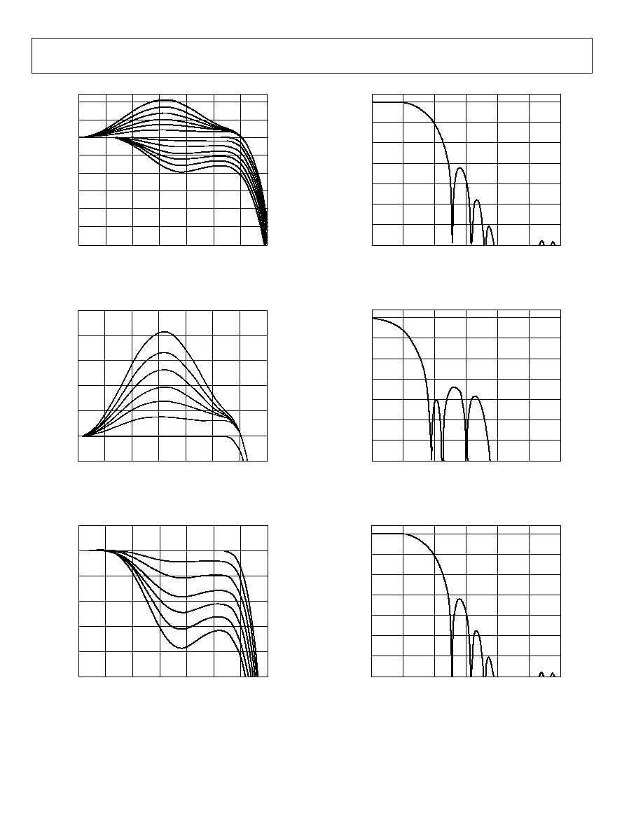
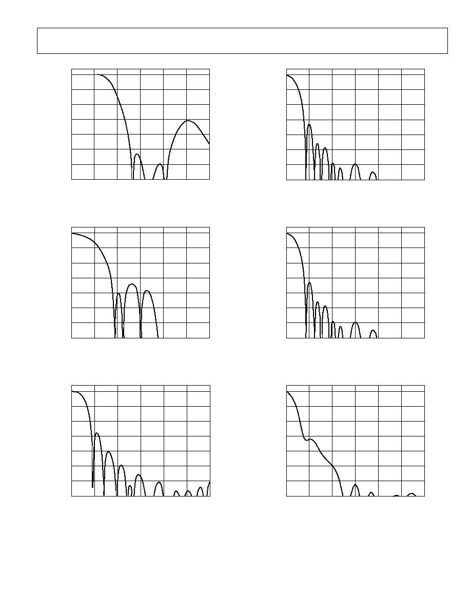
Typical Performance Characteristics ........................................... 20
MPU Port Description................................................................... 24
Register Access ................................................................................ 26
Register Programming............................................................... 26
Subaddress Register (SR7 to SR0) ............................................ 26
Input Configuration ....................................................................... 39
Standard Definition Only.......................................................... 39
Progressive Scan Only or HDTV Only ................................... 39
Simultaneous Standard Definition and Progressive Scan or
HDTV .......................................................................................... 39
Progressive Scan at 27 MHz (Dual Edge) or 54 MHz ........... 40
Features ............................................................................................ 42
Output Configuration................................................................ 42
HD Async Timing Mode ........................................................... 43
HD Timing Reset........................................................................ 44
SD Real-Time Control, Subcarrier Reset, and Timing Reset 44
Reset Sequence............................................................................ 46
SD VCR FF/RW Sync................................................................. 46
Vertical Blanking Interval ......................................................... 47
Subcarrier Frequency Registers ................................................ 47
Square Pixel Timing Mode........................................................ 48
Filters............................................................................................ 49
Color Controls and RGB Matrix .............................................. 50
Programmable DAC Gain Control .......................................... 54
Gamma Correction .................................................................... 54
HD Sharpness Filter and Adaptive Filter Controls ................ 56
HD Sharpness Filter and Adaptive Filter Application
Examples...................................................................................... 57
SD Digital Noise Reduction ...................................................... 58
Coring Gain Border ................................................................... 59
Coring Gain Data ....................................................................... 59
DNR Threshold .......................................................................... 59
Border Area ................................................................................. 59
Block Size Control...................................................................... 59
DNR Input Select Control......................................................... 59
DNR Mode Control ................................................................... 60
Block Offset Control .................................................................. 60
SD Active Video Edge ................................................................ 60
SAV/EAV Step Edge Control .................................................... 60
Board Design and Layout.............................................................. 62
DAC Termination and Layout Considerations ...................... 62
Video Output Buffer and Optional Output Filter.................. 62
PCB Board Layout...................................................................... 63
Appendix 1--Copy Generation Management System .............. 65
PS CGMS..................................................................................... 65
HD CGMS................................................................................... 65
SD CGMS .................................................................................... 65
Function of CGMS Bits ............................................................. 65
CGMS Functionality .................................................................. 65
Appendix 2--SD Wide Screen Signaling..................................... 68
Appendix 3--SD Closed Captioning ........................................... 69
Appendix 4--Test Patterns............................................................ 70
Appendix 5--SD Timing Modes .................................................. 73
Mode 0 (CCIR-656)--Slave Option (Timing Register 0 TR0 =
X X X X X 0 0 0) ......................................................................... 73
Mode 0 (CCIR-656)--Master Option (Timing Register 0 TR0
= X X X X X 0 0 1)...................................................................... 74

Preliminary Technical Data
ADV7322
Rev. PrA | Page 3 of 88
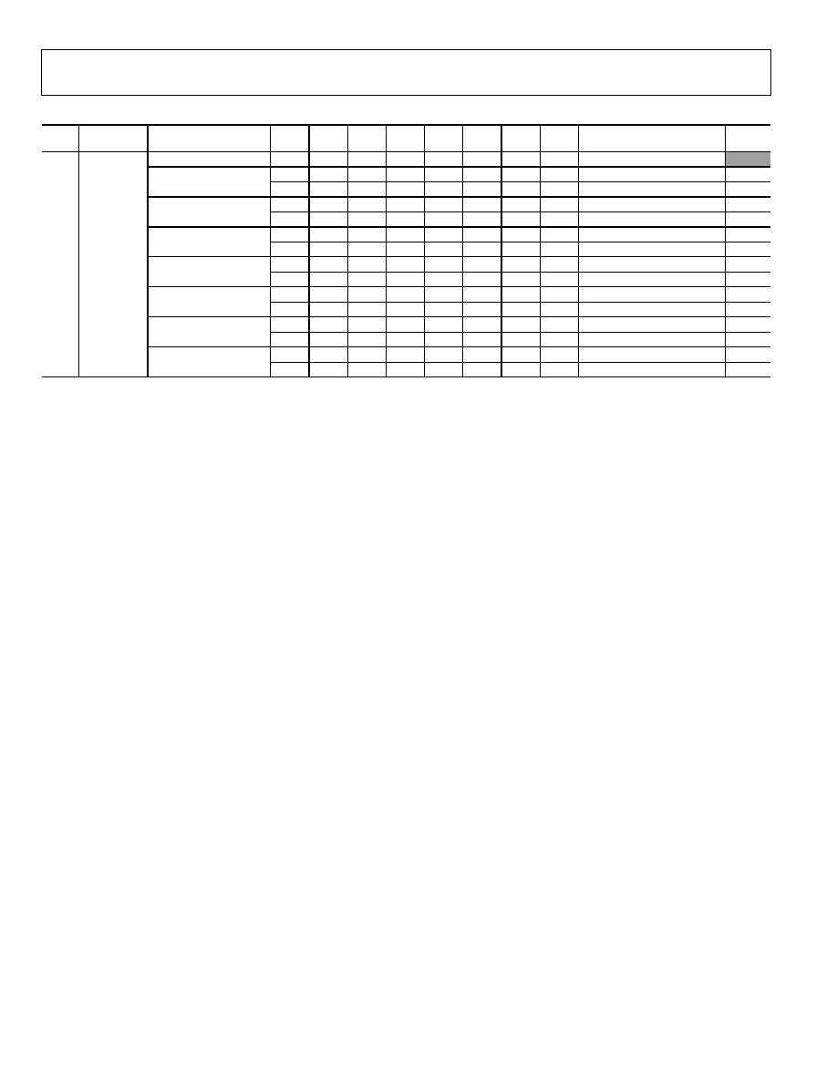
Mode 1--Slave Option (Timing Register 0 TR0 = X X X X X
0 1 0) .............................................................................................76
Mode 1--Master Option (Timing Register 0 TR0 = X X X X
X 0 1 1)..........................................................................................77
Mode 2-- Slave Option (Timing Register 0 TR0 = X X X X X
1 0 0) .............................................................................................78
Mode 2--Master Option (Timing Register 0 TR0 = X X X X
X 1 0 1)..........................................................................................79
Mode 3--Master/Slave Option (Timing Register 0 TR0 = X
X X X X 1 1 0 or X X X X X 1 1 1) ...........................................80
Appendix 6--HD Timing ..............................................................81
Appendix 7--Video Output Levels...............................................82
HD YPrPb Output Levels...........................................................82
RGB Output Levels .....................................................................83
YPrPb Levels--SMPTE/EBU N10............................................84
Appendix 8--Video Standards ......................................................86
Outline Dimensions........................................................................88
Ordering Guide ...........................................................................88
REVISION HISTORY
9/04--PrA: Preliminary Version
ADV7322
Preliminary Technical Data
Rev. PrA | Page 4 of 88
DETAILED FEATURES
High definition programmable features (720p/1080i/1035i)
2× oversampling (148.5 MHz)
Internal test pattern generator
Color hatch, black bar, flat field/frame
Fully programmable YCrCb to RGB matrix
Gamma correction
Programmable adaptive filter control
Programmable sharpness filter control
CGMS-A (720p/1080i)
Enhanced definition programmable features (525p/625p)
8× oversampling (216 MHz output)
Internal test pattern generator
Color hatch, black bar, flat frame
Individual Y and PrPb output delay
Gamma correction
Programmable adaptive filter control
Fully programmable YCrCb to RGB matrix
Undershoot limiter
Macrovision Rev 1.2 (525p/625p)
CGMS-A (525p/625p)
Standard definition programmable features
16× oversampling (216 MHz)
Internal test pattern generator
Color bars, black bar
Controlled edge rates for start and end of active video
Individual Y and PrPb output delay
Undershoot limiter
Gamma correction
Digital noise reduction (DNR)
Multiple chroma and luma filters
Luma-SSAFTM filter with programmable gain/attenuation
PrPb SSAFTM
Separate pedestal control on component and
composite/S-video output
VCR FF/RW sync mode
Macrovision Rev 7.1.L1
CGMS/WSS
Closed captioning
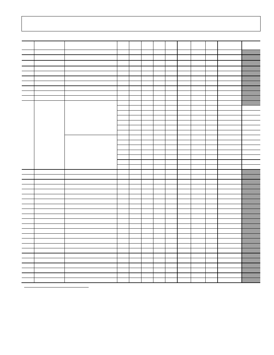
Table 1. Standards Directly Supported
1
Resolution
Interlace/
Prog.
Frame
Rate (Hz)
CLK
Input
(MHz)
Standard
720 × 480
I
29.97
27
ITU-R BT.656
720 × 576
I
25
27
ITU-R BT.656
720 × 480
I
29.97
24.54
NTSC
Square Pixel
720 × 576
I
25
29.5
PAL Square
Pixel
720 × 483
P
59.94
27
SMPTE
293M
720 × 483
P
59.94
27
BTA T-1004
720 × 483
P
59.94
27
ITU-R
BT.1358
720 × 576
P
50
27
ITU-R
BT.1358
720 × 483
P
59.94
27
ITU-R
BT.1362
720 × 576
P
50
27
ITU-R
BT.1362
30 74.25
1920 × 1035
I
29.97 74.1758
SMPTE
240M
60, 50, 30,
25, 24,
74.25,
1280 × 720
P
23.97,
59.94,
29.97
74.1758
SMPTE
296M
30, 25
74.25
1920 × 1080
I
29.97 74.1758
SMPTE
274M
30, 25, 24
74.25
1920 × 1080
P
23.98,
29.97,
74.1758
SMPTE
274M
1
Other standards are supported in async timing mode.
Preliminary Technical Data
ADV7322
Rev. PrA | Page 5 of 88
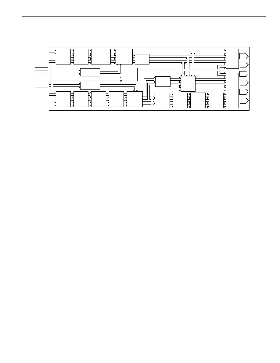
CLKIN_A
P_HSYNC
P_VSYNC
P_BLANK
S_HSYNC
S_VSYNC
S_BLANK
CLKIN_B
HD PIXEL
INPUT
SD PIXEL
INPUT
LUMA
AND
CHROMA
FILTERS
Y
CB
CR
TEST
PATTERN
DNR
GAMMA
SYNC
INSERTION
PS 8
×
HDTV 2
×
RGB
MATRIX
SD 16
×
2
×
OVER-
SAMPLING
DAC
DAC
DAC
DAC
DAC
DAC
F
SC
MODU-
LATION
CGMS
WSS
COLOR
CONTROL
DE-
INTER-
LEAVE
Y
CB
CR
DE-
INTER-
LEAVE
TEST
PATTERN
Y COLOR
CR COLOR
CB COLOR
TIMING
GENERATOR
TIMING
GENERATOR
CLOCK
CONTROL
AND PLL
4:2:2
TO
4:4:4
SHARPNESS
AND
ADAPTIVE
FILTER
CONTROL
05067-002
UV SSAF
V
U
Figure 2. Detailed Functional Block Diagram
TERMINOLOGY
SD: standard definition video, conforming to
ITU-R BT.601/ITU-R BT.656.
HD: high definition video, i.e., 720p/1080i/1035i.
EDTV: enhanced definition television (525p/625p)
PS: progressive scan video, conforming to SMPTE 293M,
ITU-R BT.1358, BTAT-1004EDTV2, or ITU-R BT.13621362.
HDTV: high definition television video, conforming to SMPTE
274M, or SMPTE 296M and SMPTE240M.
YCrCb SD, PS, or HD component: digital video.
YPrPb SD, PS, or HD component: analog video.

ADV7322
Preliminary Technical Data
Rev. PrA | Page 6 of 88
SPECIFICATIONS
V
AA
= 2.375 V - 2.625 V, V
DD
= 2.375 V - 2.625 V, V
DD_IO
= 2.375 V - 3.6 V, V
REF
= 1.235 V, R
SET
= 3040 , R
LOAD
= 300 . All specifications
T
MIN
to T
MAX
(0°C to 70°C), unless otherwise noted.
Table 2.
Parameter
Min
Typ
Max
Unit
Test Conditions
STATIC PERFORMANCE
1
Resolution
11
Bits
Integral Nonlinearity
1.5
LSB
Differential Nonlinearity
2
, +ve
0.5
LSB
Differential Nonlinearity
2
, -ve
1.0
LSB
DIGITAL OUTPUTS
Output Low Voltage, V
OL
0.4 [0.4]
3
V I
SINK
= 3.2 mA
Output High Voltage, V
OH
2.4[2.0]
3
V I
SOURCE
= 400 µA
Three-State Leakage Current
±1.0
µA V
IN
= 0.4 V, 2.4 V
Three-State Output Capacitance
2
pF
DIGITAL AND CONTROL INPUTS
Input High Voltage, V
IH
2
V
Input Low Voltage, V
IL
0.8 V
Input Leakage Current
10
µA V
IN
= 2.4 V
Input Capacitance, C
IN
2
pF
ANALOG OUTPUTS
Full-Scale Output Current
4.1
4.33
4.6
mA
Output Current Range
4.1
4.33
4.6
mA
DAC to DAC Matching
1.0
%
Output Compliance Range, V
OC
0 1.0
1.4 V
Output Capacitance, C
OUT
7
pF
VOLTAGE REFERENCE
Internal Reference Range, V
REF
1.15 1.235
1.3 V
External Reference Range, V
REF
1.15 1.235
1.3 V
V
REF
Current
4
±10
µA
POWER REQUIREMENTS
Normal Power Mode
I
DD
5
137
mA
SD only [16×]
78
mA
PS only [8×]
73
mA
HDTV only [2×]
140
190
6
mA
SD[16×, 8 bit] + PS[8×, 16 bit]
I
DD_IO
1.0
mA
I
AA
7,
8
37
45
mA
Sleep Mode
I
DD
80
µA
I
AA
7
µA
I
DD_IO
250
µA
POWER SUPPLY REJECTION RATIO
0.01
%/%
1
Oversampling disabled. Static DAC performance will be improved with increased oversampling ratios.
2
DNL measures the deviation of the actual DAC output voltage step from the ideal. For +ve DNL, the actual step value lies above the ideal step value; for -ve DNL, the
actual step value lies below the ideal step value.
3
Value in brackets for V
DD_IO
= 2.375 V - 2.75 V.
4
External current required to overdrive internal V
REF
.
5
I
DD
, the circuit current, is the continuous current required to drive the digital core.
6
Guaranteed maximum by characterization.
7
All DACs on.
8
I
AA
is the total current required to supply all DACs including the V
REF
circuitry and the PLL circuitry.
Preliminary Technical Data
ADV7322
Rev. PrA | Page 7 of 88
DYNAMIC SPECIFICATIONS
V
AA
= 2.375 V - 2.625 V, V
DD
= 2.375 V - 2.625 V, V
DD_IO
= 2.375 V - 3.6 V, V
REF
= 1.235 V, R
SET
= 3040 , R
LOAD
= 300 . All specifications
T
MIN
to T
MAX
(0°C to 70°C), unless otherwise noted.
Table 3.
Parameter
Min
Typ
Max
Unit
Test Conditions
PROGRESSIVE SCAN MODE
Luma Bandwidth
12.5
MHz
Chroma Bandwidth
5.8
MHz
SNR
65.6
dB
Luma ramp unweighted
72
dB
Flat field full bandwidth
HDTV MODE
Luma Bandwidth
30
MHz
Chroma Bandwidth
13.75
MHz
STANDARD DEFINITION MODE
Hue Accuracy
0.4
Degrees
Color Saturation Accuracy
0.4
%
Chroma Nonlinear Gain
1.2
±%
Referenced to 40 IRE
Chroma Nonlinear Phase
-0.2
± Degrees
Chroma/Luma Intermodulation
0
±%
Chroma/Luma Gain Inequality
97
±%
Chroma/Luma Delay Inequality
-1.1
ns
Luminance Nonlinearity
0.5
±%
Chroma AM Noise
84
dB
Chroma PM Noise
75.2
dB
Differential Gain
0.15
%
NTSC
Differential Phase
0.2
Degrees
NTSC
SNR
59.1
dB
Luma ramp
77.1
dB
Flat field full bandwidth

ADV7322
Preliminary Technical Data
Rev. PrA | Page 8 of 88
TIMING SPECIFICATIONS
V
AA
= 2.375 V - 2.625 V, V
DD
= 2.375 V - 2.625 V, V
DD_IO
= 2.375 V - 3.6 V, V
REF
= 1.235 V, R
SET
= 3040 , R
LOAD
= 300 . All specifications
T
MIN
to T
MAX
(0°C to 70°C), unless otherwise noted.
Table 4.
Parameter
Min
Typ
Max
Unit
Test Conditions
MPU PORT
1
SCLOCK Frequency
0
400 kHz
SCLOCK High Pulse Width, t
1
0.6
µs
SCLOCK Low Pulse Width, t
2
1.3
µs
Hold Time (Start Condition), t
3
0.6
µs
First clock generated after this period relevant
for repeated start condition
Setup Time (Start Condition), t
4
0.6
µs
Data Setup Time, t
5
100
ns
SDATA, SCLOCK Rise Time, t
6
300 ns
SDATA, SCLOCK Fall Time, t
7
300 ns
Setup Time (Stop Condition), t
8
0.6
µs
RESET Low Time
100
ns
ANALOG OUTPUTS
Analog Output Delay
2
7
ns
Output Skew
1
ns
CLOCK CONTROL AND PIXEL PORT
3
f
CLK
29.5
MHz
SD PAL square pixel mode
f
CLK
81
MHz
PS/HD async mode
Clock High Time, t
9
40
% of one clk cycle
Clock Low Time, t
10
40
% of one clk cycle
Data Setup Time, t
11
1
2.0
ns
Data Hold Time, t
12
1
2.0
ns
SD Output Access Time, t
13
15 ns
SD Output Hold Time, t
14
5.0
ns
HD Output Access Time, t
13
14 ns
HD Output Hold Time, t
14
5.0
ns
PIPELINE DELAY
4
63
clk cycles
SD [2×, 16×]
76
clk cycles
SD component mode [16×]
35
clk cycles
PS [1×]
41
clk cycles
PS [8×]
36
clk cycles
HD [2×, 1×]
1
Guaranteed by characterization.
2
Output delay measured from the 50% point of the rising edge of CLOCK to the 50% point of DAC output full-scale transition.
3
Data: C[9:0]; Y[9:0], S[9:0]
Control: P_HSYNC, P_VSYNC, P_BLANK, S_HSYNC, S_VSYNC, S_BLANK
4
SD, PS = 27 MHz, HD = 74.25 MHz.
Preliminary Technical Data
ADV7322
Rev. PrA | Page 9 of 88
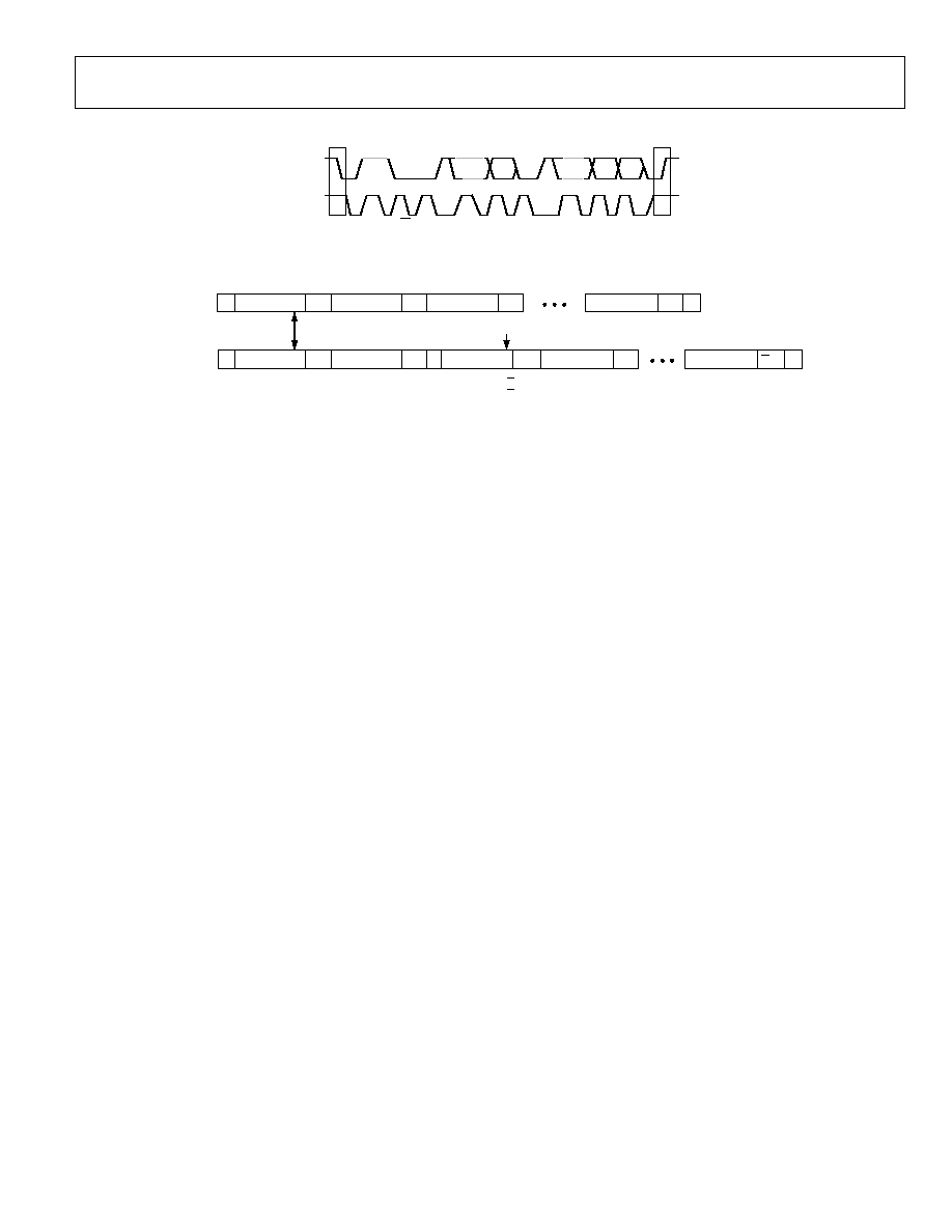
TIMING DIAGRAMS
t
9
t
11
CLKIN_A
C7C0
t
10
t
12
CONTROL
INPUTS
Y0
Y1
Y2
Y3
Y4
Y5
Y7Y0
t
14
CONTROL
OUTPUTS
t
13
t
9
= CLOCK HIGH TIME
t
10
= CLOCK LOW TIME
t
11
= DATA SETUP TIME
t
12
= DATA HOLD TIME
P_HSYNC,
P_VSYNC,
P_BLANK
Cr4
Cb4
Cr2
Cb2
Cr0
Cb0
05067-
003
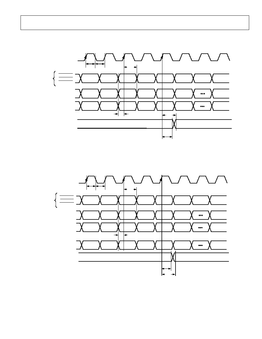
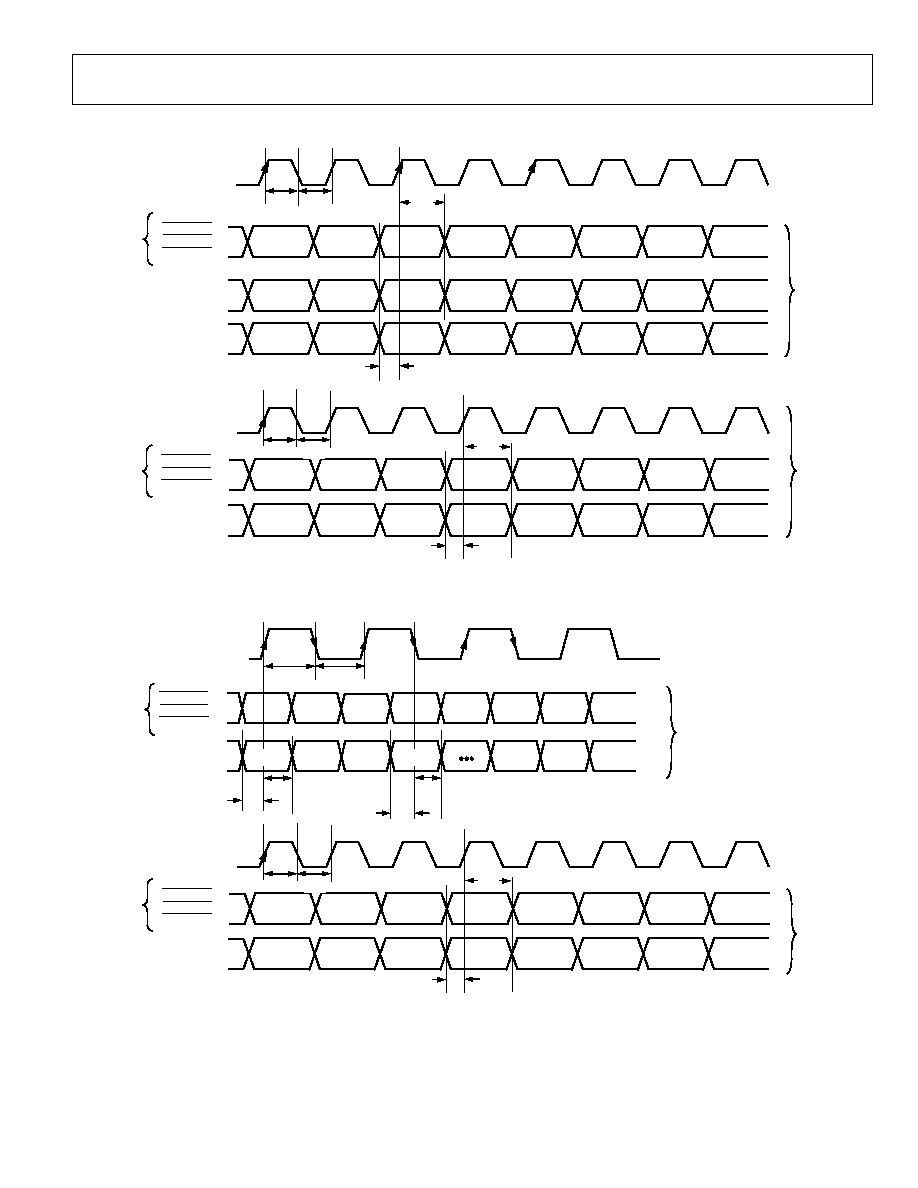
Figure 3. HD Only 4:2:2 Input Mode [Input Mode 010]; PS Only 4:2:2 Input Mode [Input Mode 001]
t
9
t
11
CLKIN_A
C7C0
t
10
t
12
CONTROL
INPUTS
Y0
Y1
Y2
Y3
Y4
Y5
Y7Y0
t
14
CONTROL
OUTPUTS
t
13
t
9
= CLOCK HIGH TIME
t
10
= CLOCK LOW TIME
t
11
= DATA SETUP TIME
t
12
= DATA HOLD TIME
S7S0
Cr4
Cr3
Cr2
Cr1
Cr0
Cr5
Cb4
Cb3
Cb2
Cb1
Cb0
Cb5
P_HSYNC,
P_VSYNC,
P_BLANK
05067-
004
Figure 4. HD Only 4:4:4 Input Mode [Input Mode 010]; PS Only 4:4:4 Input Mode [Input Mode 001]
ADV7322
Preliminary Technical Data
Rev. PrA | Page 10 of 88
t
9
t
11
CLKIN_A
C7C0
t
10
t
12
P_HSYNC,
P_VSYNC,
P_BLANK
CONTROL
INPUTS
G0
G1
G2
G3
G4
G5
B0
B1
B2
B3
B4
B5
R0
R1
R2
R3
R4
R5
Y7Y0
t
14
CONTROL
OUTPUTS
t
13
t
9
= CLOCK HIGH TIME
t
10
= CLOCK LOW TIME
t
11
= DATA SETUP TIME
t
12
= DATA HOLD TIME
S7S0
05067-
005
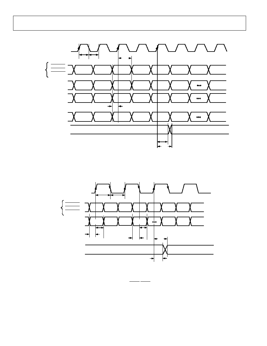
Figure 5. HD RGB 4:4:4 Input Mode [Input Mode 010]
t
9
t
11
t
10
t
12
t
11
t
12
t
13
t
14
CLKIN_B*
*CLKIN_B MUST BE USED IN THIS PS MODE.
Y7Y0
t
9
= CLOCK HIGH TIME
t
10
= CLOCK LOW TIME
t
11
= DATA SETUP TIME
t
12
= DATA HOLD TIME
CONTROL
INPUTS
CONTROL
OUTPUTS
Yxxx
Crxxx
Y1
Cr0
Y0
Cb0
P_HSYNC,
P_VSYNC,
P_BLANK
05067-
006
Figure 6. PS 4:2:2 8-Bit Interleaved at 27 MHz HSYNC/VSYNC Input Mode [Input Mode 100]
Preliminary Technical Data
ADV7322
Rev. PrA | Page 11 of 88
t
9
t
11
t
10
t
12
t
14
t
13
CLKIN_A
Y7Y0
t
9
= CLOCK HIGH TIME
t
10
= CLOCK LOW TIME
t
11
= DATA SETUP TIME
t
12
= DATA HOLD TIME
CONTROL
INPUTS
CONTROL
OUTPUTS
Yxxx
Crxxx
Y1
Cr0
Y0
Cb0
P_VSYNC,
P_HSYNC,
P_BLANK
05067-
007
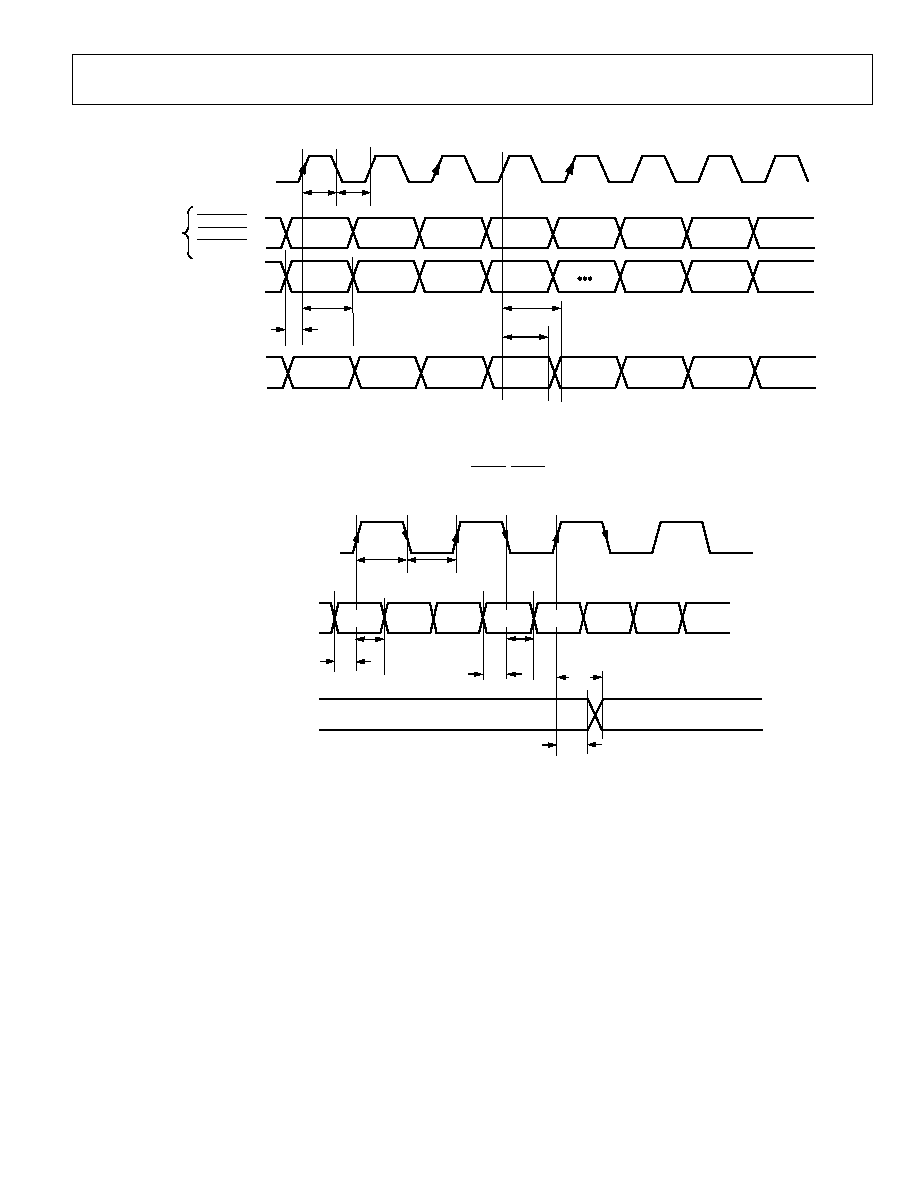
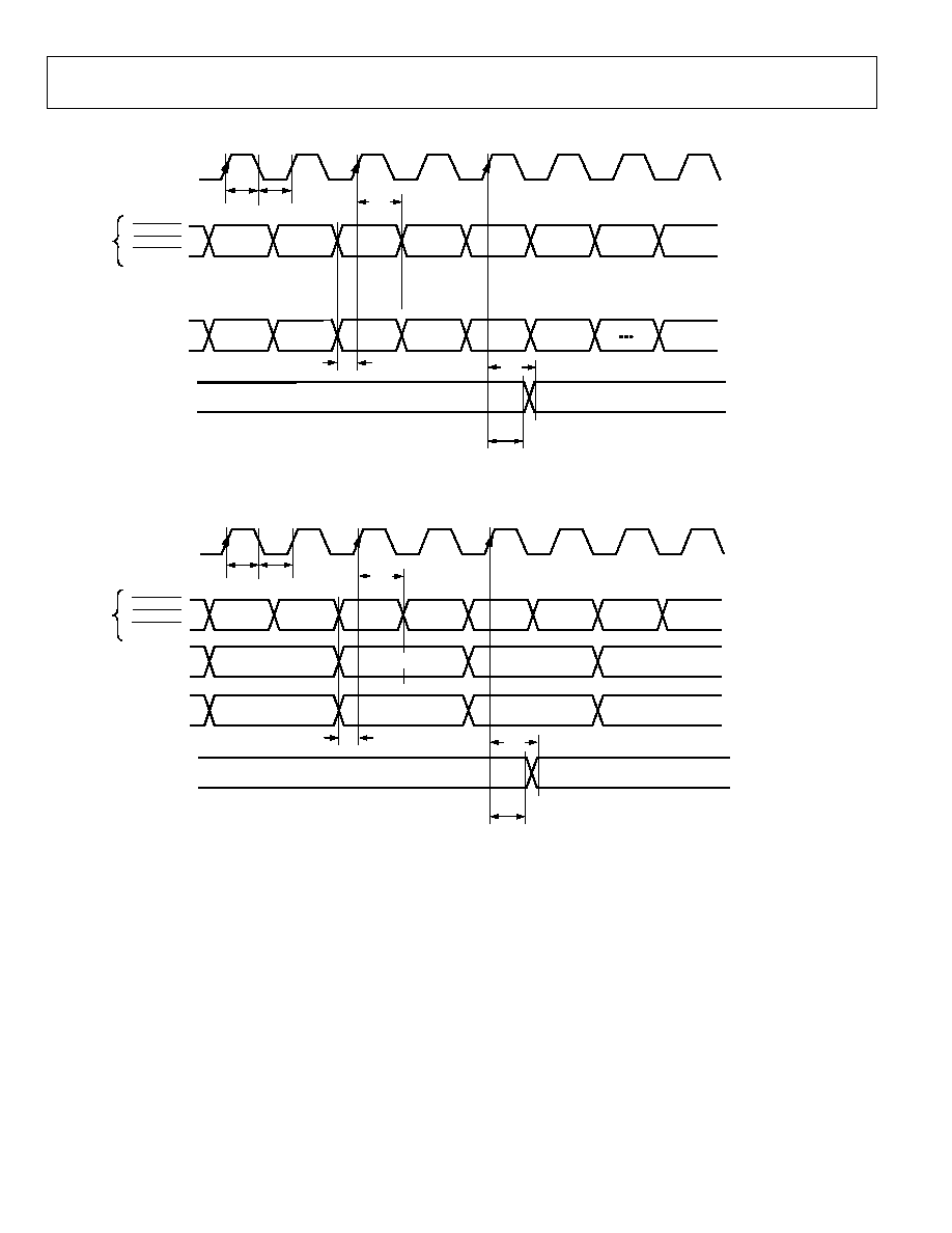
Figure 7. PS 4:2:2 8-Bit Interleaved at 54 MHz HSYNC /VSYNC Input Mode [Input Mode 111]
t
9
t
11
t
10
t
12
t
11
t
12
t
13
t
14
CLKIN_B*
*CLKIN_B USED IN THIS PS ONLY MODE.
Y7Y0
t
9
= CLOCK HIGH TIME
t
10
= CLOCK LOW TIME
t
11
= DATA SETUP TIME
t
12
= DATA HOLD TIME
CONTROL
OUTPUTS
Y1
Cr0
Y0
Cb0
XY
00
00
FF
05067-
008
Figure 8. PS Only 4:2:2 8-Bit Interleaved at 27 MHz EAV/SAV Input Mode [Input Mode 100]
ADV7322
Preliminary Technical Data
Rev. PrA | Page 12 of 88
t
9
t
11
t
10
t
12
t
14
t
13
CLKIN_A
Y7Y0
t
9
= CLOCK HIGH TIME
t
10
= CLOCK LOW TIME
t
11
= DATA SETUP TIME
t
12
= DATA HOLD TIME
CONTROL
OUTPUTS
NOTE: Y0, Cb0 SEQUENCE AS PER SUBADDRESS 0x01 BIT-1
FF
00
00
XY
Cb0
Y0
Cr0
Y1
05067-
009
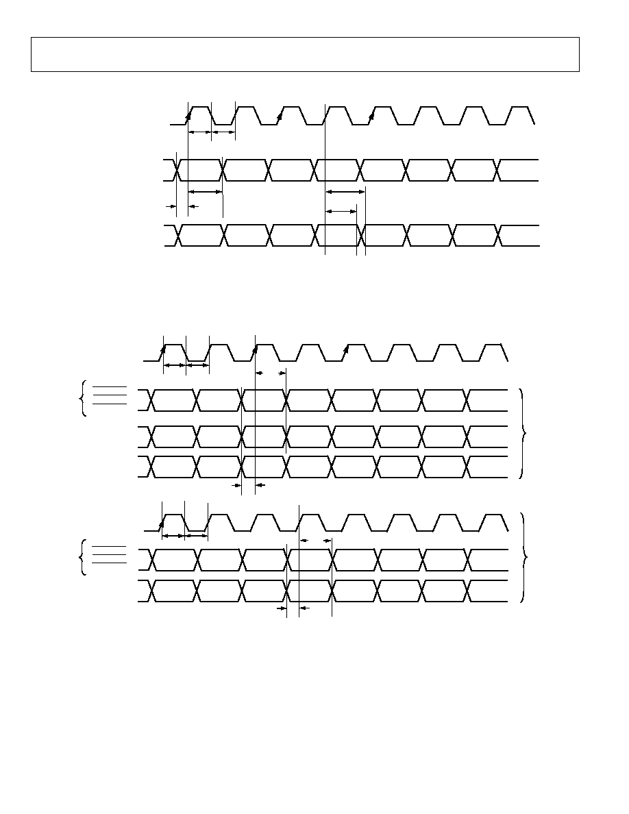
Figure 9. PS Only 4:2:2 8-Bit Interleaved at 54 MHz EAV/SAV Input Mode [Input Mode 111]
t
9
t
11
t
10
t
12
Y0
Y1
Y2
Y3
Y4
Y5
t
9
t
10
t
11
t
12
HD INPUT
SD INPUT
S7S0
CONTROL
INPUTS
CLKIN_A
CLKIN_B
Y7Y0
CONTROL
INPUTS
C7C0
P_HSYNC,
P_VSYNC,
P_BLANK
Y2
Cb1
Y1
Cr0
Y0
Cb0
S_HSYNC,
S_VSYNC,
S_BLANK
Cr4
Cb4
Cr2
Cb2
Cr0
Cb0
05067-
010
Figure 10. HD 4:2:2 and SD (8-Bit) Simultaneous Input Mode [Input Mode 101: SD Oversampled] [Input Mode 110: HD Oversampled]
Preliminary Technical Data
ADV7322
Rev. PrA | Page 13 of 88
t
9
t
11
t
10
t
12
Y0
Y1
Y2
Y3
Y4
Y5
t
9
t
10
t
11
t
12
PS INPUT
SD INPUT
S7S0
CONTROL
INPUTS
CLKIN_A
CLKIN_B
Y7Y0
CONTROL
INPUTS
C7C0
P_HSYNC,
P_VSYNC,
P_BLANK
Y2
Cb1
Y1
Cr0
Y0
Cb0
S_HSYNC,
S_VSYNC,
S_BLANK
Cr4
Cb4
Cr2
Cb2
Cr0
Cb0
05067-
011
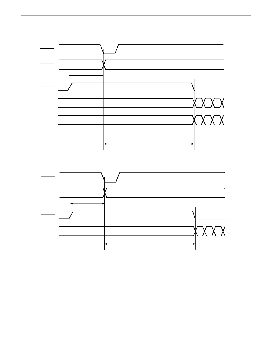
Figure 11. PS (4:2:2) and SD (8-Bit) Simultaneous Input Mode [Input Mode 011]
t
9
t
11
t
10
t
12
t
11
t
12
CLKIN_B
Y7Y0
CONTROL
INPUTS
Yxxx
Crxxx
Y1
Cr0
Y0
Cb0
P_HSYNC,
P_VSYNC,
P_BLANK
PS INPUT
t
9
t
10
t
11
t
12
SD INPUT
S7S0
CONTROL
INPUTS
CLKIN_A
Y2
Cb1
Y1
Cr0
Y0
Cb0
S_HSYNC,
S_VSYNC,
S_BLANK
05067-
012
Figure 12. PS (8-Bit) and SD (8-Bit) Simultaneous Input Mode [Input Mode 100]
ADV7322
Preliminary Technical Data
Rev. PrA | Page 14 of 88
t
9
t
11
CLKIN_A
t
10
t
12
CONTROL
INPUTS
t
14
CONTROL
OUTPUTS
t
13
S_HSYNC,
S_VSYNC,
S_BLANK
Cr4
Cb4
Cr2
Cb2
Cr0
Cb0
05067-
013
S7S0/Y7Y0*
*SELECTED BY ADDRESS 0x01 BIT 7
IN MASTER/SLAVE MODE
IN SLAVE MODE
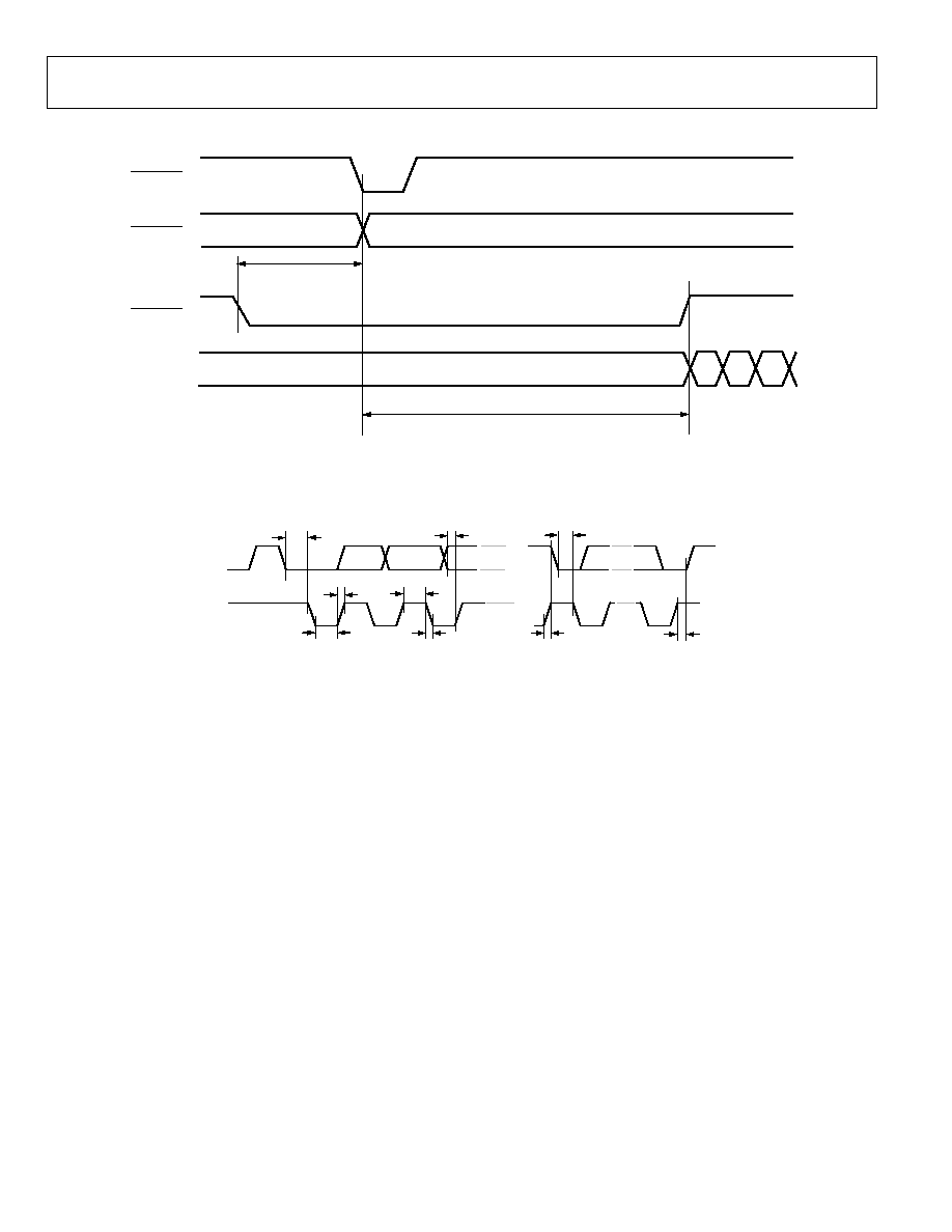
Figure 13. 8-Bit SD Only Pixel Input Mode [Input Mode 000]
t
9
t
11
CLKIN_A
C7C0*
t
10
t
12
Cb0
Cr0
Cb2
Cr2
CONTROL
INPUTS
t
14
CONTROL
OUTPUTS
t
13
*SELECTED BY ADDRESS 0x01 BIT 7: See Table 21.
IN MASTER/SLAVE MODE
IN SLAVE MODE
S7S0/Y7Y0*
Y0
Y2
Y3
Y1
S_HSYNC,
S_VSYNC,
S_BLANK
05067-014
Figure 14. 16-Bit SD Only Pixel Input Mode [Input Mode 000]
Preliminary Technical Data
ADV7322
Rev. PrA | Page 15 of 88
Y7Y0
Y0
Y1
Y2
Y3
b
a
a AND b AS PER RELEVANT STANDARD
C7C0
Cb1
Cr1
Cr0
Cb0
P_HSYNC
P_VSYNC
P_BLANK
05067-
015
Figure 15. HD 4:2:2 Input Timing Diagram
Y7Y0
Cb
Y
Cr
Y
b
a
a = 32 CLKCYCLES FOR 525p
a = 24 CLKCYCLES FOR 625p
AS RECOMMENDED BY STANDARD
b(MIN) = 244 CLKCYCLES FOR 525p
b(MIN) = 264 CLKCYCLES FOR 625p
P_HSYNC
P_VSYNC
P_BLANK
05067-
016
Figure 16. PS 4:2:2 8-Bit Interleaved Input Timing Diagram
ADV7322
Preliminary Technical Data
Rev. PrA | Page 16 of 88
Cb
Y
Cr
Y
PAL = 24 CLK CYCLES
NTSC = 32 CLK CYCLES
PAL = 24 CLK CYCLES
NTSC = 32 CLK CYCLES
S7S0/Y7Y0*
*SELECTED BY ADDRESS 0x01 BIT 7
S_HSYNC
S_VSYNC
S_BLANK
05067-
017
Figure 17. SD Timing Input for Timing Mode 1
t
3
t
1
t
6
t
2
t
7
t
5
SDA
SCLK
t
3
t
4
t
8
05067-018
Figure 18. MPU Port Timing Diagram
Preliminary Technical Data
ADV7322
Rev. PrA | Page 17 of 88
ABSOLUTE MAXIMUM RATINGS
Table 5.
Parameter
1
Value
V
AA
to AGND
-0.3 V to +3.0 V
V
DD
to DGND
-0.3 V to +3.0 V
V
DD_IO
to GND_IO
-0.3 V to 4.6 V
Digital Input Voltage to DGND
-0.3 V to V
DD_IO
+0.3 V
V
AA
to V
DD
-0.3 V to +0.3 V
AGND to DGND
-0.3 V to +0.3 V
DGND to GND_IO
-0.3 V to +0.3 V
AGND to GND_IO
-0.3 V to +0.3 V
Ambient Operating Temperature (T
A
)
0°C to 70°C
Storage Temperature (T
S
)
65°C to +150°C
Infrared Reflow Soldering (20 s)
260°C
1
Analog output short circuit to any power supply or common can be of
an indefinite duration.
Stresses above those listed under Absolute Maximum Ratings
may cause permanent damage to the device. This is a stress
rating only; functional operation of the device at these or any
other conditions above those listed in the operational sections
of this specification is not implied. Exposure to absolute
maximum rating conditions for extended periods may affect
device reliability.
THERMAL CHARACTERISTICS
JC
= 11°C/W
JA
= 47°C/W
The ADV7322 is a Pb-free environmentally friendly product. It
is manufactured using the most up-to-date materials and
processes. The coating on the leads of each device is 100% pure
Sn electroplate. The device is suitable for Pb-free applications
and is able to withstand surface-mount soldering at up to 255°C
(±5°C).
In addition, it is backward-compatible with conventional SnPb
soldering processes. This means that the electroplated Sn
coating can be soldered with Sn/Pb solder pastes at
conventional reflow temperatures of 220°C to 235°C.
ESD CAUTION
ESD (electrostatic discharge) sensitive device. Electrostatic charges as high as 4000 V readily
accumulate on the human body and test equipment and can discharge without detection. Although
this product features proprietary ESD protection circuitry, permanent damage may occur on devices
subjected to high energy electrostatic discharges. Therefore, proper ESD precautions are
recommended to avoid performance degradation or loss of functionality.
ADV7322
Preliminary Technical Data
Rev. PrA | Page 18 of 88
PIN CONFIGURATION AND FUNCTION DESCRIPTIONS
64
GND_
IO
63
CLKIN_
B
62
S7
61
S6
60
S5
59
S4
58
S3
57
DGND
56
V
DD
55
S2
54
S1
53
S0
52
TEST5
51
TEST4
50
S_HSYNC
49
S_VSYNC
47
R
SET1
46
V
REF
45
COMP1
42
DAC C
43
DAC B
44
DAC A
48
S_BLANK
41
V
AA
40
AGND
39
DAC D
37
DAC F
36
COMP2
35
R
SET2
34
EXT_LF
33
RESET
38
DAC E
2
TEST0
3
TEST1
4
Y0
7
Y3
6
Y2
5
Y1
1
V
DD_IO
8
Y4
9
Y5
10
V
DD
12
Y6
13
Y7
14
TEST2
15
TEST3
16
C0
11
DGND
17
C1
18
C2
19
I
2
C
20
ALSB
21
SDA
22
SCLK
23
P_HSYNC
24
P_VSYNC
25
P_
BLANK
26
C3
27
C4
28
C5
29
C6
30
C7
31
RTC_
SCR_
TR
32
CLKIN_
A
PIN 1
ADV7322
TOP VIEW
(Not to Scale)
05067-
019
Figure 19. Pin Configuration
Preliminary Technical Data
ADV7322
Rev. PrA | Page 19 of 88
Table 6. Pin Function Descriptions
Mnemonic
Input/Output Function
DGND
G
Digital Ground.
AGND
G
Analog Ground.
CLKIN_A
I
Pixel Clock Input for HD (74.25 MHz Only, PS Only (27 MHz), SD Only (27 MHz).
CLKIN_B
I
Pixel Clock Input. Requires a 27 MHz reference clock for progressive scan mode or a 74.25 MHz (74.1758
MHz) reference clock in HDTV mode. This clock is only used in dual modes.
COMP1,
COMP2
O
Compensation Pin for DACs. Connect 0.1 µF capacitor from COMP pin to V
AA
.
DAC A
O
CVBS/Green/Y/Y Analog Output.
DAC B
O
Chroma/Blue/U/Pb Analog Output.
DAC C
O
Luma/Red/V/Pr Analog Output.
DAC D
O
In SD Only Mode: CVBS/Green/Y Analog Output; in HD Only Mode and Simultaneous HD/SD Mode:
Y/Green [HD] Analog Output.
DAC E
O
In SD Only Mode: Luma/Blue/U Analog Output; in HD Only Mode and Simultaneous HD/SD Mode: Pr/Red
Analog Output.
DAC F
O
In SD Only Mode: Chroma/Red/V Analog Output; in HD Only Mode and Simultaneous HD/SD Mode:
Pb/Blue [HD] Analog Output.
P_HSYNC
I
Video Horizontal Sync Control Signal for HD in Simultaneous SD/HD Mode and HD Only Mode.
P_VSYNC
I
Video Vertical Sync Control Signal for HD in Simultaneous SD/HD Mode and HD Only Mode.
P_BLANK
I
Video Blanking Control Signal for HD in Simultaneous SD/HD Mode and HD Only Mode.
S_BLANK
I/O
Video Blanking Control Signal for SD Only.
S_HSYNC
I/O
Video Horizontal Sync Control Signal for SD Only.
S_VSYNC
I/O
Video Vertical Sync Control Signal for SD Only.
Y7 to Y0
I
SD or Progressive Scan/HDTV Input Port for Y Data. Input port for interleaved progressive scan data. The
LSB is set up on Pin Y0.
C7 to C0
I
Progressive Scan/HDTV Input Port 4:4:4 Input Mode. This port is used for the Cb [Blue/U] data. The LSB is
set up on Pin C0.
S7 to S0
I
SD or Progressive Scan/HDTV Input Port for Cr [Red/V] data in 4:4:4 input mode. LSB is set up on Pin S0.
RESET
I
This input resets the on-chip timing generator and sets the ADV7322 into default register setting. RESET is
an active low signal.
R
SET1
, R
SET2
I
A 3040 resistor must be connected from this pin to AGND and is used to control the amplitudes of the
DAC outputs.
SCLK
I
I
2
C Port Serial Interface Clock Input.
SDA
I/O
I
2
C Port Serial Data Input/Output.
ALSB
I
TTL Address Input. This signal sets up the LSB of the I
2
C address. When this pin is tied low, the I
2
C filter is
activated, which reduces noise on the I
2
C interface.
V
DD_IO
P
Power Supply for Digital Inputs and Outputs.
V
DD
P
Digital Power Supply.
V
AA
P
Analog Power Supply.
V
REF
I/O
Optional External Voltage Reference Input for DACs or Voltage Reference Output (1.235 V).
EXT_LF
I
External Loop Filter for the Internal PLL.
RTC_SCR_TR I
Multifunctional Input. Real time control (RTC) input, timing reset input, subcarrier reset input.
I
2
C
I
This input pin must be tied high (V
DD_IO
) for the ADV7322 to interface over the I
2
C port.
GND_IO
Digital Input/Output Ground.
TEST0 to
TEST5
I
Not used. Tie to DGND
ADV7322
Preliminary Technical Data
Rev. PrA | Page 20 of 88
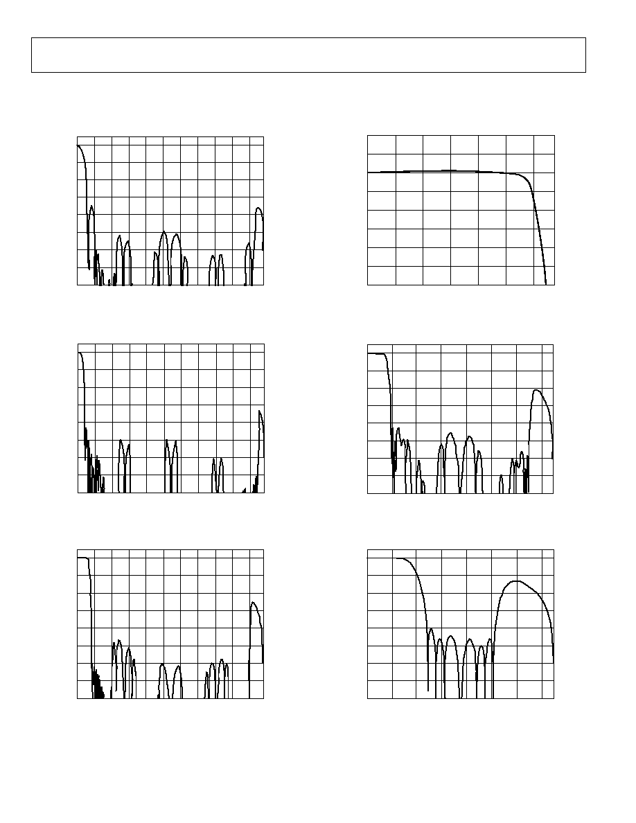
TYPICAL PERFORMANCE CHARACTERISTICS
FREQUENCY (MHz)
PROG SCAN Pr/Pb RESPONSE. LINEAR INTERP FROM 4:2:2 TO 4:4:4
0
GAIN (
d
B)
70
60
50
40
30
20
10
80
200
20
40
60
80
100
120 140
160 180
0
05067-045
Figure 20. PS--UV 8× Oversampling Filter (Linear)
FREQUENCY (MHz)
PROG SCAN Pr/Pb RESPONSE. SSAF INTERP FROM 4:2:2 TO 4:4:4
0
GAIN (
d
B)
70
60
50
40
30
20
10
80
200
20
40
60
80
100 120
140 160
180
0
05067-046
Figure 21. PS--UV 8× Oversampling Filter (SSAF)
FREQUENCY (MHz)
Y RESPONSE IN PS OVERSAMPLING MODE
0
GAIN (
d
B)
70
60
50
40
30
20
10
80
200
20
40
60
80
100
120 140
160 180
0
05067-047
Figure 22. PS--Y (8× Oversampling Filter)
FREQUENCY (MHz)
Y PASS BAND IN PS OVERSAMPLING MODE
GAIN (
d
B)
2.5
2.0
1.5
1.0
0.5
0
0.5
1.0
3.0
12
2
4
6
8
10
0
05067-048
Figure 23. PS--Y 8× Oversampling Filter (Pass Band)
FREQUENCY (MHz)
Pr/Pb RESPONSE IN HDTV OVERSAMPLING MODE
0
GAIN (
d
B)
70
60
50
40
30
20
10
80
140
20
40
60
80
100
120
0
05067-049
Figure 24. HDTV--UV (2× Oversampling Filter)
FREQUENCY (MHz)
Y RESPONSE IN HDTV OVERSAMPLING MODE
0
GAIN (
d
B)
70
60
50
40
30
20
10
80
140
20
40
60
80
100
120
0
05067-050
Figure 25. HDTV--Y (2× Oversampling Filter)
Preliminary Technical Data
ADV7322
Rev. PrA | Page 21 of 88
FREQUENCY (MHz)
MAGNITUDE
(dB)
0
12
10
8
6
4
2
0
10
30
50
60
70
20
40
05067-051
Figure 26. Luma NTSC Low-Pass Filter
FREQUENCY (MHz)
MAG
N
I
T
UDE
(dB)
0
12
10
8
6
4
2
0
10
30
50
60
70
20
40
05067-052
Figure 27. Luma PAL Low-Pass Filter
FREQUENCY (MHz)
MAGNITUDE
(dB)
0
12
10
8
6
4
2
0
10
30
50
60
70
20
40
05067-053
Figure 28. Luma NTSC Notch Filter
FREQUENCY (MHz)
MAGNITUDE
(dB)
0
12
10
8
6
4
2
0
10
30
50
60
70
20
40
05067-054
Figure 29. Luma PAL Notch Filter
FREQUENCY (MHz)
Y RESPONSE IN SD OVERSAMPLING MODE
GAIN (
d
B)
0
50
80
0
20
40
60
80
100 120 140 160 180 200
10
40
60
70
20
30
05067-055
Figure 30. Y--16× Oversampling Filter
FREQUENCY (MHz)
MAGNITUDE
(dB)
0
12
10
8
6
4
2
0
10
30
50
60
70
20
40
05067-056
Figure 31. Luma SSAF Filter up to 12 MHz
ADV7322
Preliminary Technical Data
Rev. PrA | Page 22 of 88
FREQUENCY (MHz)
4
7
MAG
N
I
T
UDE
(dB)
2
2
6
8
12
0
4
5
10
6
05067-057
0
1
2
3
4
Figure 32. Luma SSAF Filter--Programmable Responses
FREQUENCY (MHz)
7
MAGNITUDE
(dB)
5
4
2
1
1
3
5
0
6
05067-058
0
1
2
3
4
Figure 33. Luma SSAF Filter--Programmable Gain
FREQUENCY (MHz)
7
MAGNITUDE
(dB)
1
0
2
3
5
1
5
4
6
05067-059
0
1
2
3
4
Figure 34. Luma SSAF Filter--Programmable Attenuation
FREQUENCY (MHz)
0
12
MAG
N
I
T
UDE
(dB)
10
30
50
60
70
20
40
10
05067-060
8
4
6
2
0
Figure 35. Luma CIF Low-Pass Filter
FREQUENCY (MHz)
0
12
MAGNITUDE
(dB)
10
30
50
60
70
20
40
10
8
4
6
2
0
05067-061
Figure 36. Luma QCIF Low-Pass Filter
FREQUENCY (MHz)
0
12
MAGNITUDE
(dB)
10
30
50
60
70
20
40
10
8
4
6
2
0
05067-062
Figure 37. Chroma 3.0 MHz Low-Pass Filter
Preliminary Technical Data
ADV7322
Rev. PrA | Page 23 of 88
FREQUENCY (MHz)
0
12
MAGNITUDE
(dB)
10
30
50
60
70
20
40
10
8
4
6
2
0
05067-063
Figure 38. Chroma 2.0 MHz Low-Pass Filter
FREQUENCY (MHz)
0
12
MAGNITUDE
(dB)
10
30
50
60
70
20
40
10
8
4
6
2
0
05067-064
Figure 39. Chroma 1.3 MHz Low-Pass Filter
FREQUENCY (MHz)
0
12
MAGNITUDE
(dB)
10
30
50
60
70
20
40
10
8
4
6
2
0
05067-065
Figure 40. Chroma 1.0 MHz Low-Pass Filter
FREQUENCY (MHz)
0
12
MAG
N
I
T
UDE
(dB)
10
30
50
60
70
20
40
10
8
4
6
2
0
05067-066
Figure 41. Chroma 0.65 MHz Low-Pass Filter
FREQUENCY (MHz)
0
12
MAGNITUDE
(dB)
10
30
50
60
70
20
40
10
8
4
6
2
0
05067-067
Figure 42. Chroma CIF Low-Pass Filter
FREQUENCY (MHz)
0
12
MAGNITUDE
(dB)
10
30
50
60
70
20
40
10
8
4
6
2
0
05067-068
Figure 43. Chroma QCIF Low-Pass Filter
ADV7322
Preliminary Technical Data
Rev. PrA | Page 24 of 88
MPU PORT DESCRIPTION
The ADV7322 supports a 2-wire serial (I
2
C-compatible)
microprocessor bus driving multiple peripherals. This port
operates in an open-drain configuration. Two inputs, serial data
(SDA) and serial clock (SCL), carry information between any
device connected to the bus and the ADV7322. Each slave
device is recognized by a unique address. The ADV7322 has
four possible slave addresses for both read and write operations.
These are unique addresses for each device and are illustrated in
Figure 44. The LSB sets either a read or write operation. Logic 1
corresponds to a read operation, while Logic 0 corresponds to a
write operation. A1 is set by setting the ALSB pin of the
ADV7322 to Logic 0 or Logic 1. When ALSB is set to 1, there is
greater input bandwidth on the I
2
C lines, which allows high
speed data transfers on this bus. When ALSB is set to 0, there is
reduced input bandwidth on the I
2
C lines, which means that
pulses of less than 50 ns will not pass into the I
2
C internal
controller. This mode is recommended for noisy systems.
1
1
0
1
0
1
A1
X
ADDRESS
CONTROL
SET UP BY
ALSB
READ/WRITE
CONTROL
0 WRITE
1 READ
05067-020
Figure 44. ADV7322 Slave Address = 0xD4
To control the various devices on the bus, the following protocol
must be followed. First the master initiates a data transfer by
establishing a start condition, defined by a high-to-low
transition on SDA while SCL remains high. This indicates that
an address/data stream will follow. All peripherals respond to
the start condition and shift the next eight bits (7-bit address +
R/W bit). The bits are transferred from MSB down to LSB. The
peripheral that recognizes the transmitted address responds by
pulling the data line low during the ninth clock pulse. This is
known as an acknowledge bit. All other devices withdraw from
the bus at this point and maintain an idle condition. The idle
condition is where the device monitors the SDA and SCL lines
waiting for the start condition and the correct transmitted
address. The R/W bit determines the direction of the data.
Logic 0 on the LSB of the first byte means that the master will
write information to the peripheral. Logic 1 on the LSB of the
first byte means that the master will read information from the
peripheral.
The ADV7322 acts as a standard slave device on the bus. The
data on the SDA pin is eight bits long, supporting the 7-bit
addresses plus the R/W bit. It interprets the first byte as the
device address and the second byte as the starting subaddress.
There is a subaddress auto-increment facility. This allows data
to be written to or read from registers in ascending subaddress
sequence starting at any valid subaddress. A data transfer is
always terminated by a stop condition. The user can also access
any unique subaddress register on a one-by-one basis without
having to update all the registers.
Stop and start conditions can be detected at any stage during
the data transfer. If these conditions are asserted out of
sequence with normal read and write operations, then they
cause an immediate jump to the idle condition. During a given
SCL high period, the user should only issue one start condition,
one stop condition, or a single stop condition followed by a
single start condition. If an invalid subaddress is issued by the
user, the ADV7322 will not issue an acknowledge and will
return to the idle condition. If in auto-increment mode the user
exceeds the highest subaddress, the following action is taken:
1.
In read mode, the highest subaddress register contents are
output until the master device issues a no-acknowledge.
This indicates the end of a read. A no-acknowledge
condition is when the SDA line is not pulled low on the
ninth pulse.
2.
In write mode, the data for the invalid byte is not loaded
into any subaddress register, a no-acknowledge is issued by
the ADV7322, and the part returns to the idle condition.
Before writing to the subcarrier frequency registers, it is a
requirement that the ADV7322 is reset at least once after
power-up.
The four subcarrier frequency registers must be updated,
starting with subcarrier frequency register 0 through subcarrier
frequency register 3. The subcarrier frequency will not update
until the last subcarrier frequency register byte has been
received by the ADV7322.
Figure 45 illustrates an example of data transfer for a write
sequence and the start and stop conditions. Figure 46 shows bus
write and read sequences.
Preliminary Technical Data
ADV7322
Rev. PrA | Page 25 of 88
SDATA
SCLOCK
START ADRR R/W ACK SUBADDRESS ACK
DATA
ACK
STOP
17
8
9
S
17
17
P
05067-022
8
9
8
9
Figure 45. Bus Data Transfer
WRITE
SEQUENCE
READ
SEQUENCE
S SLAVE ADDR A(S)
SUBADDR
A(S)
DATA
DATA
A(S) P
S SLAVE ADDR A(S)
SUBADDR
A(S) S SLAVE ADDR A(S)
DATA
DATA
A(M)
A(M) P
S = START BIT
P = STOP BIT
A(S) = ACKNOWLEDGE BY SLAVE
A(M) = ACKNOWLEDGE BY MASTER
A (S) = NO-ACKNOWLEDGE BY SLAVE
A (M) = NO-ACKNOWLEDGE BY MASTER
LSB = 0
LSB = 1
05067-023
A(S)
Figure 46. Read and Write Sequence
ADV7322
Preliminary Technical Data
Rev. PrA | Page 26 of 88
REGISTER ACCESS
The MPU can write to or read from all of the registers of the
ADV7322 except the subaddress registers, which are write only
registers. The subaddress register determines which register the
next read or write operation will access. All communications
with the part through the bus start with an access to the
subaddress register. A read/write operation is then performed
from/to the target address, which increments to the next
address until a stop command is performed on the bus.
REGISTER PROGRAMMING
The following tables describe the functionality of each register.
All registers can be read from as well as written to, unless
otherwise stated.
SUBADDRESS REGISTER (SR7 TO SR0)
The communication register is an 8-bit write-only register. After
the part is accessed over the bus and a read/write operation is
selected, the subaddress is set up. The subaddress register
determines to/from which register the operation takes place.
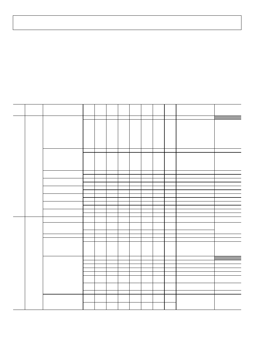
Table 7. Registers 0x00 to 0x01
SR7
SR0
Register
Bit Description
Bit 7
Bit 6
Bit 5
Bit 4
Bit 3
Bit 2
Bit 1
Bit 0
Register Setting
Reg. Reset
Values
(Shaded)
0
Sleep
mode
off.
0xFC
Sleep Mode. With this
control enabled, the
current consumption is
reduced to µA level. All
DACs and the internal PLL
cct are disabled. I
2
C
registers can be read from
and written to in sleep
mode.
1
Sleep mode on.
0
PLL
on.
PLL and Oversampling
Control. This control
allows the internal PLL cct
to be powered down and
the oversampling to be
switched off.
1
PLL
off.
0
DAC
F
off.
DAC F: Power On/Off.
1
DAC F on.
0
DAC
E
off.
DAC E: Power On/Off.
1
DAC
E
on.
0
DAC
D
off.
DAC D: Power On/Off.
1
DAC D on.
0
DAC D off.
DAC C: Power On/Off.
1
DAC
C
on.
0
DAC B off.
DAC B: Power On/Off.
1
DAC B on.
0
DAC
A
off.
0x00
Power
Mode
Register
DAC A: Power On/Off.
1
DAC
A
on.
Reserved
0
Reserved
0
Cb
clocked
on
rising
edge.
Clock Edge.
1
Y clocked on rising edge
Only for PS
interleaved
input at 27 MHz.
Reserved.
0
0
Clock Align.
1
Must be set if the phase
delay between the two
input clocks is
<9.25 ns or >27.75 ns.
Only if two
input clocks are
used.
0
0
0
SD input only.
0x38
0
0
1
PS input only.
0
1
0
HDTV input only.
0
1
1
SD and PS [16-bit].
1
0
0
SD and PS [8-bit].
1
0
1
SD and HDTV [SD
oversampled].
1
1
0
SD and HDTV [HDTV
oversampled].
Input Mode.
1
1
1
PS only [at 54 MHz].
0
0x01 Mode
Select
Register
Y/C/S Bus Swap.
1
Allows data to be
applied to data ports in
various configurations
(SD feature only).
See Table 21.
Preliminary Technical Data
ADV7322
Rev. PrA | Page 27 of 88
Table 8. Registers 0x02 to 0x0F
SR7
SR0
Register
Bit Description
Bit 7
Bit 6
Bit 5
Bit 4
Bit 3
Bit 2
Bit 1
Bit 0
Register Setting
Reset Values
Reserved
0
0
Zero must be written to
these bits.
0x20
0
Disabled.
Test Pattern Black
Bar
1
Enabled.
0x11, Bit 2 must
also be enabled.
0
Disable
manual
RGB
matrix
adjust.
Manual RGB
Matrix Adjust
1
Enable
manual
RGB
matrix
adjust.
0
No sync.
Sync on RGB
1
1
Sync on all RGB outputs.
0
RGB component outputs.
RGB/YPrPb
Output
1
YPrPb component outputs.
0
No Sync output.
SD Sync
1
Output SD syncs on
S_HSYNC, S_VSYNC,
S_BLANK pins.
0
No sync output.
0x02
Mode Register 0
HD Sync
1
Output HD,ED, syncs on
S_HSYNC, S_VSYNC.
0x03
RGB Matrix 0
x
x
LSB for GY.
0x03
x
x
LSB for RV.
0xF0
x
x
LSB for BU.
x
x
LSB for GV.
0x04
RGB Matrix 1
x
x
LSB for GU.
0x05
RGB Matrix 2
x
x
x
x
x
x
x
x
Bits 92 for GY.
0x4E
0x06
RGB Matrix 3
x
x
x
x
x
x
x
x
Bits 92 for GU.
0x0E
0x07
RGB Matrix 4
x
x
x
x
x
x
x
x
Bits 92 for GV.
0x24
0x08
RGB Matrix 5
x
x
x
x
x
x
x
x
Bits 92 for BU.
0x92
0x09
RGB Matrix 6
x
x
x
x
x
x
x
x
Bits 92 for RV.
0x7C
0x0A
DAC A, B, C Output
Level
2
Positive Gain to
DAC Output
Voltage
0
0
0
0
0
0
0
0
0%
0x00
0
0
0
0
0
0
0
1
+0.018%
0
0
0
0
0
0
1
0
0.036%
...
...
0
0
1
1
1
1
1
1
+7.382%
0
1
0
0
0
0
0
0
+7.5%
Negative
Gain
to
DAC Output
Voltage
1
1
0
0
0
0
0
0
-7.5%
1
1
0
0
0
0
0
1
-7.382%
1
0
0
0
0
0
1
0
-7.364%
...
...
1
1
1
1
1
1
1
1
-0.018%
0x0B
DAC D, E, F Output
Level
Positive Gain to
DAC Output
Voltage
0
0
0
0
0
0
0
0
0%
0x00
0
0
0
0
0
0
0
1
+0.018%
0
0
0
0
0
0
1
0
0.036%
...
...
0
0
1
1
1
1
1
1
+7.382%
0
1
0
0
0
0
0
0
+7.5%
Negative
Gain
to
DAC Output
Voltage
1
1
0
0
0
0
0
0
-7.5%
1
1
0
0
0
0
0
1
-7.382%
1
0
0
0
0
0
1
0
-7.364%
...
...
1
1
1
1
1
1
1
1
-0.018%
0x0C
Reserved
0x00
0x0D
Reserved
0x00
0x0E
Reserved
0x00
0x0F
Reserved
0x00
1
For more detail, refer to Appendix 7.
2
For more detail on the programmable output levels, refer to the Programmable DAC Gain Control section.
ADV7322
Preliminary Technical Data
Rev. PrA | Page 28 of 88
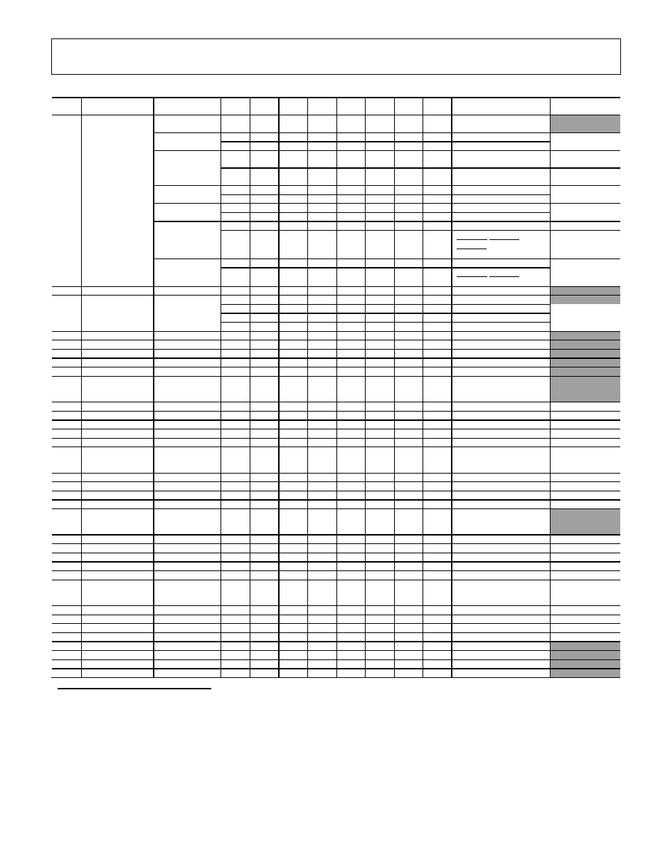
Table 9. Registers 0x10 to 0x11
SR7
SR0
Register
Bit Description
Bit 7
Bit 6
Bit 5
Bit 4
Bit 3
Bit 2
Bit 1
Bit 0
Register Setting
Note
Reset
Values
0
0
EIA770.2
output
0x00
0
1
EIA770.1
output
1
0
Output levels for
full input range
HD Output
Standard
1
1
Reserved
0
HSYNC, VSYNC,
BLANK
Input Sync
Format
1
EAV/SAV
codes
0 0 0 0 0 SMPTE 293M, ITU-
BT 1358
525p @
59.94 Hz
0 0 0 0 1 Async
mode
0 0 0 1 0 BTA-1004, ITU-
BT 1362
525p @
59.94 Hz
0 0 0 1 1 ITU-BT
1358 625p @
50 Hz
0 0 1 0 0 ITU-BT
1362 625p @
50 Hz
0 0 1 0 1 SMPTE
296M-1,
2
720p @
60/59.94 Hz
0 0 1 1 0 SMPTE
296M-3
720p @
50 Hz
0 0 1 1 1 SMPTE
296M-4,
5
720p @
30/29.97 Hz
0 1 0 0 0 SMPTE
296M-6
720p @
25 Hz
0 1 0 0 1 SMPTE
296M-7,
8
720p @
24/23.98 Hz
0 1 0 1 0 SMPTE
240M
1035i @
60/59.94 Hz
0 1 0 1 1 Reserved
0 1 1 0 0 Reserved
0 1 1 0 1 SMPTE
274M-4,5
1080i @
30/29.97 Hz
0 1 1 1 0 SMPTE
274M-6
1080i @
25 Hz
0 1 1 1 1 SMPTE
274M-7,
8
1080p @
30/29.97 Hz
1 0 0 0 0 SMPTE
274M-9
1080p @
25 Hz
1 0 0 0 1 SMPTE 274M-
10, 11
1080p @
24/23.98 Hz
0x10
HD Mode
Register 1
HD/ED Input
Mode
1001011111
Reserved
0
Pixel
data
valid
off
1
Pixel
data
valid
on
0x00
HD Pixel Data
Valid
0
Reserved
0
HD
test
pattern
off
HD Test Pattern
Enable
1
HD
test
pattern
on
0
Hatch
HD Test Pattern
Hatch/Field
1
Field/frame
0
Disabled
HD VBI Open
1
Enabled
0
0
Disabled
0
1
-11 IRE
1
0
-6 IRE
HD Undershoot
Limiter
1
1
-1.5 IRE
Only
available in
EDTV
(525p/625p)
0
Disabled
0x11
HD Mode
Register 2
HD Sharpness
Filter
1
Enabled
Preliminary Technical Data
ADV7322
Rev. PrA | Page 29 of 88
Table 10. Register 0x12
SR7
SR0
Register
Bit Description
Bit 7
Bit 6
Bit 5
Bit 4
Bit 3
Bit 2
Bit 1
Bit 0
Register Setting
Reset
Values
0
0
0
0 clk cycles
0x00
0
0
1
1 clk cycles
0
1
0
2 clk cycles
0
1
1
3 clk cycles
HD Y Delay with Respect
to Falling Edge of HSYNC
1
0
0
4 clk cycles
0
0
0
0 clk cycles
0
0
1
1 clk cycle
0
1
0
2 clk cycles
0
1
1
3 clk cycles
HD Color Delay with
Respect to Falling Edge of
HSYNC
1
0
0
4 clk cycles
0
Disabled
HD CGMS
1
Enabled
0
Disabled
0x12
HD Mode
Register
3
HD CGMS CRC
1
Enabled
Table 11. Registers 0x13 to 0x14
SR7
SR0
Register
Bit Description
Bit 7
Bit 6
Bit 5
Bit 4
Bit 3
Bit 2
Bit 1
Bit 0
Register Setting
Reset
Values
0
Cb after falling edge of HSYNC.
0x4C
HD Cr/Cb Sequence
1
Cr
after
falling
edge
of
HSYNC.
Reserved
0
0 must be written to this bit.
Reserved
0
0 must be written here
0
Disabled.
Sinc Filter on DAC D, E, F
1
Enabled.
Reserved
0
0 must be written to this bit.
0
Disabled.
HD Chroma SSAF
1
Enabled.
0
4:4:4
HD Chroma Input
1
4:2:2
0
Disabled.
0x13
HD Mode
Register 4
HD Double Buffering
1
Enabled.
HD Timing Reset
x
A low-high-low transition
resets the internal HD timing
counters.
0x00
0
Signal duration on S_Hsync
same as ADV731x.
HD Hsync Generation
1
1
Signal duration on S_Hsync =
sync duration on embedded Y.
0
Field signal out on S_Vsync pin.
HD Vsync Generation
1
1
Vsync Signal. Duration = Vsync
on embedded Y.
0
BLANK active high.
HD Blank Polarity
1
BLANK active low.
0
Macrovision
disabled.
HD Macrovision for 525p
and 625p
1
Macrovision
enabled.
Reserved
0
0 must be written to these bits.
0
0 = field input.
HD VSYNC/Field Input
1
1
=
VSYNC input.
0
Update Horizontal/Vertical
counters.
0x14
HD Mode
Register 5
Horizontal/Vertical
counters
2
1
Horizontal/Vertical counters
free running.
1
Used in conjunction with HD_SYNC in Register 0x02, Bit 7 set to 1.
2
When set to 0, the Horizontal/Vertical counters automatically wrap around at the end of the Line/field/frame of the standard selected. When set to 1, the
Horizontal/Vertical counters are free running and wrap around when external sync signals indicate so.
ADV7322
Preliminary Technical Data
Rev. PrA | Page 30 of 88
Table 12. Register 0x15
SR7
SR0
Register
Bit Description
Bit 7
Bit 6
Bit 5
Bit 4
Bit 3
Bit 2
Bit 1
Bit 0
Register Setting
Reset
Values
Reserved
0
0 must be written to this bit
0x00
0
Disabled
HD RGB Input
1
Enabled
0
Disabled
HD Sync on PrPb
1
Enabled
0
DAC
E
=
Pb;
DAC
F
=
Pr
HD Color DAC Swap
1
DAC
E
=
Pr;
DAC
F
=
Pb
0
Gamma
Curve
A
HD Gamma Curve A/B
1
Gamma
Curve
B
0
Disabled
HD Gamma Curve Enable
1
Enabled
0
Mode A
HD Adaptive Filter Mode
1
Mode B
0
Disabled
0x15
HD Mode
Register 6
HD Adaptive Filter Enable
1
Enabled
Preliminary Technical Data
ADV7322
Rev. PrA | Page 31 of 88
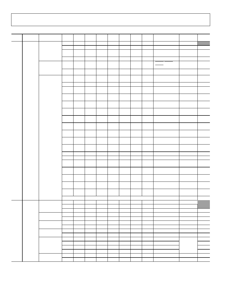
Table 13. Registers 0x16 to 0x37
SR7
SR0
Register
Bit Description
Bit 7
Bit 6
Bit 5
Bit 4
Bit 3
Bit 2
Bit 1
Bit 0
Register
Setting
Reset
Values
0x16
HD Y Level
1
x
x
x
x
x
x
x
x
Y level value
0xA0
0x17
HD Cr Level
1
x
x
x
x
x
x
x
x
Cr level value
0x80
0x18
HD Cb Level
1
x
x
x
x
x
x
x
x
Cb level value
0x80
0x19
Reserved
0x00
0x1A
Reserved
0x00
0x1B
Reserved
0x00
0x1C
Reserved
0x00
0x1D
Reserved
0x00
0x1E
Reserved
0x00
0x1F
Reserved
0x00
0
0
0
0
Gain A = 0
0x00
0
0
0
1
Gain A = +1
...
...
... ...
...
0
1
1
1
Gain A = +7
1
0
0
0
Gain A = -8
...
...
... ...
...
HD Sharpness Filter Gain Value A
1
1
1
1
Gain A = -1
0
0
0
0
Gain B = 0
0
0
0
1
Gain B = +1
... ... ... ...
...
0
1
1
1
Gain B = +7
1
0
0
0
Gain B = -8
... ... ... ...
...
0x20
HD Sharpness
Filter Gain
HD Sharpness Filter Gain Value B
1
1
1
1
Gain B = -1
0x21
HD CGMS Data 0
HD CGMS Data Bits
0
0
0
0
C19
C18
C17
C16
CGMS 1916
0x00
0x22
HD CGMS Data 1
HD CGMS Data Bits
C15
C14
C13
C12
C11
C10
C9
C8
CGMS 158
0x00
0x23
HD CGMS Data 2
HD CGMS Data Bits
C7
C6
C5
C4
C3
C2
C1
C0
CGMS 70
0x00
0x24
HD Gamma A
HD Gamma Curve A Data Points
x
x
x
x
x
x
x
x
A0
0x00
0x25
HD Gamma A
HD Gamma Curve A Data Points
x
x
x
x
x
x
x
x
A1
0x00
0x26
HD Gamma A
HD Gamma Curve A Data Points
x
x
x
x
x
x
x
x
A2
0x00
0x27
HD Gamma A
HD Gamma Curve A Data Points
x
x
x
x
x
x
x
x
A3
0x00
0x28
HD Gamma A
HD Gamma Curve A Data Points
x
x
x
x
x
x
x
x
A4
0x00
0x29
HD Gamma A
HD Gamma Curve A Data Points
x
x
x
x
x
x
x
x
A5
0x00
0x2A
HD Gamma A
HD Gamma Curve A Data Points
x
x
x
x
x
x
x
x
A6
0x00
0x2B
HD Gamma A
HD Gamma Curve A Data Points
x
x
x
x
x
x
x
x
A7
0x00
0x2C
HD Gamma A
HD Gamma Curve A Data Points
x
x
x
x
x
x
x
x
A8
0x00
0x2D
HD Gamma A
HD Gamma Curve A Data Points
x
x
x
x
x
x
x
x
A9
0x00
0x2E
HD Gamma B
HD Gamma Curve B Data Points
x
x
x
x
x
x
x
x
B0
0x00
0x2F
HD Gamma B
HD Gamma Curve B Data Points
x
x
x
x
x
x
x
x
B1
0x00
0x30
HD Gamma B
HD Gamma Curve B Data Points
x
x
x
x
x
x
x
x
B2
0x00
0x31
HD Gamma B
HD Gamma Curve B Data Points
x
x
x
x
x
x
x
x
B3
0x00
0x32
HD Gamma B
HD Gamma Curve B Data Points
x
x
x
x
x
x
x
x
B4
0x00
0x33
HD Gamma B
HD Gamma Curve B Data Points
x
x
x
x
x
x
x
x
B5
0x00
0x34
HD Gamma B
HD Gamma Curve B Data Points
x
x
x
x
x
x
x
x
B6
0x00
0x35
HD Gamma B
HD Gamma Curve B Data Points
x
x
x
x
x
x
x
x
B7
0x00
0x36
HD Gamma B
HD Gamma Curve B Data Points
x
x
x
x
x
x
x
x
B8
0x00
0x37
HD Gamma B
HD Gamma Curve B Data Points
x
x
x
x
x
x
x
x
B9
0x00
1
For use with internal test pattern only.
ADV7322
Preliminary Technical Data
Rev. PrA | Page 32 of 88
Table 14. Registers 0x38 to 0x3D
SR7
SR0
Register
Bit Description
Bit 7
Bit 6
Bit 5
Bit 4
Bit 3
Bit 2
Bit 1
Bit 0
Register
Setting
Reset
Values
0
0
0
0
Gain A = 0
0x00
0
0
0
1
Gain A = +1
...
...
...
...
...
0
1
1
1
Gain A = +7
1
0
0
0
Gain A = -8
...
...
...
...
...
HD Adaptive
Filter Gain 1
Value A
1
1
1
1
Gain A = -1
0
0
0
0
Gain B = 0
0
0
0
1
Gain B = +1
... ... ... ...
...
0
1
1
1
Gain B = +7
1
0
0
0
Gain B = -8
... ... ... ...
...
0x38
HD Adaptive Filter
Gain 1
HD Adaptive
Filter Gain 1
Value B
1
1
1
1
Gain B = -1
0
0
0
0
Gain A = 0
0x00
0
0
0
1
Gain A = +1
...
...
...
...
...
0
1
1
1
Gain A = +7
1
0
0
0
Gain A = -8
...
...
...
...
...
HD Adaptive
Filter Gain 2
Value A
1
1
1
1
Gain A = -1
0
0
0
0
Gain B = 0
0
0
0
1
Gain B = +1
... ... ... ...
...
0
1
1
1
Gain B = +7
1
0
0
0
Gain B = -8
... ... ... ...
...
0x39
HD Adaptive Filter
Gain 2
HD Adaptive
Filter Gain 2
Value B
1
1
1
1
Gain B = -1
0
0
0
0
Gain A = 0
0x00
0
0
0
1
Gain A = +1
...
...
...
...
...
0
1
1
1
Gain A = +7
1
0
0
0
Gain A = -8
...
...
...
...
...
HD Adaptive
Filter Gain 3
Value A
1
1
1
1
Gain A = -1
0
0
0
0
Gain B = 0
0
0
0
1
Gain B = +1
... ... ... ...
...
0
1
1
1
Gain B = +7
1
0
0
0
Gain B = -8
... ... ... ...
...
0x3A
HD Adaptive Filter
Gain 3
HD Adaptive
Filter Gain 3
Value B
1
1
1
1
Gain B = -1
0x3B
HD Adaptive Filter
Threshold A
HD Adaptive
Filter Threshold
A Value
x
x
x
x
x
x
x
x
Threshold A
0x00
0x3C
HD Adaptive Filter
Threshold B
HD Adaptive
Filter Threshold
B Value
x
x
x
x
x
x
x
x
Threshold B
0x00
0x3D
HD Adaptive Filter
Threshold C
HD Adaptive
Filter Threshold
C Value
x
x
x
x
x
x
x
x
Threshold C
0x00
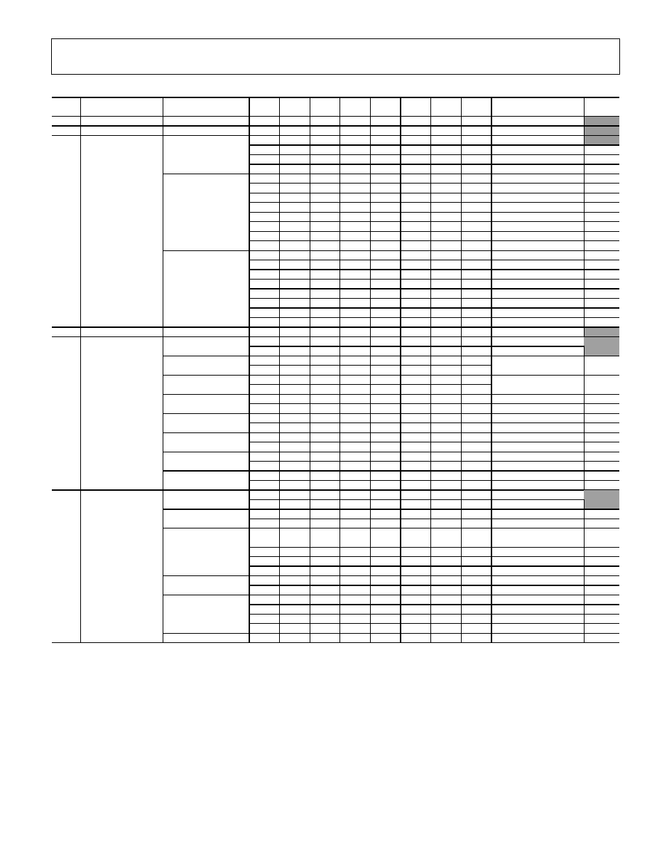
Preliminary Technical Data
ADV7322
Rev. PrA | Page 33 of 88
Table 15. Registers 0x3E to 0x43
SR7
SR0
Register
Bit Description
Bit 7
Bit 6
Bit 5
Bit 4
Bit 3
Bit 2
Bit 1
Bit 0
Register Setting
Reset
Values
0x3E
Reserved
0x00
0x3F
Reserved
0x00
0
0
NTSC
0x00
0
1
PAL B, D, G, H, I
1
0
PAL M
SD Standard
1
1
PAL N
0
0
0
LPF NTSC
0
0
1
LPF PAL
0
1
0
Notch NTSC
0
1
1
Notch PAL
1
0
0
SSAF luma
1
0
1
Luma CIF
1
1
0
Luma QCIF
SD Luma Filter
1
1
1
Reserved
0
0
0
1.3 MHz
0
0
1
0.65 MHz
0
1
0
1.0 MHz
0
1
1
2.0 MHz
1
0
0
Reserved
1
0
1
Chroma CIF
1
1
0
Chroma QCIF
0x40
SD Mode Register 0
SD Chroma Filter
1
1
1
3.0 MHz
0x41
Reserved
0x00
0
Disabled
SD PrPb SSAF
1
Enabled
0x08
0
SD DAC Output 1
1
Refer to output
configuration section
0
SD DAC Output 2
1
Refer to output
configuration section
0
Disabled
SD Pedestal
1
Enabled
0
Disabled
SD Square Pixel
1
Enabled
0
Disabled
SD VCR FF/RW Sync
1
Enabled
0
Disabled
SD Pixel Data Valid
1
Enabled
0
Disabled
0x42
SD Mode Register 1
SD SAV/EAV Step
Edge Control
1
Enabled
0
No pedestal on YUV
SD Pedestal YPrPb
Output
1
7.5
IRE
pedestal
on
YUV
0x00
0
Y = 700 mV/300 mV
SD Output Levels Y
1
Y = 714 mV/286 mV
0
0
700
mV
p-p[PAL];
1000 mV p-p[NTSC]
0
1
700 mV p-p
1
0
1000 mV p-p
SD Output Levels PrPb
1
1
648 mV p-p
0
Disabled
SD VBI Open
1
Enabled
0
0
CC
disabled
0
1
CC on odd field only
1
0
CC on even field only
SD CC Field Control
1
1
CC on both fields
0x43
SD Mode Register 2
Reserved
0
Reserved
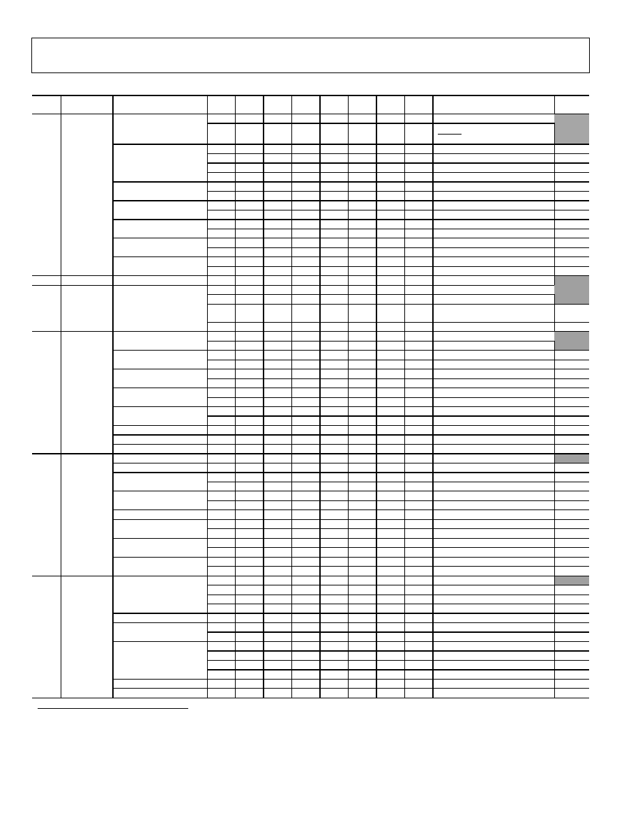
ADV7322
Preliminary Technical Data
Rev. PrA | Page 34 of 88
Table 16. Registers 0x44 to 0x49
SR7
SR0
Register
Bit Description
Bit 7
Bit 6
Bit 5
Bit 4
Bit 3
Bit 2
Bit 1
Bit 0
Register Setting
Reset
Values
0
Disabled
SD VSYNC-3H
1
VSYNC= 2.5 lines [PAL],
VSYNC= 3 lines [NTSC]
0x00
0
0
Genlock
disabled
0
1
Subcarrier
Reset
1
0
Timing
Reset
SD RTC/TR/SCR
1
1
RTC
enabled
0
720
pixels
SD Active Video Length
1
710
[NTSC]/702[PAL]
0
Chroma
enabled
SD Chroma
1
Chroma
disabled
0
Enabled
SD Burst
1
Disabled
0
Disabled
SD Color Bars
1
Enabled
0
DAC A = luma, DAC B = chroma
0x44 SD
Mode
Register 3
SD DAC Swap
1
DAC A = chroma, DAC B = luma
0x45
Reserved
0x00
0
0
5.17
µs
0
1
5.31
µs
(default)
0x01
1
0
5.59
µs
(must
be
set
for
Macrovision compliance)
0x46 SD
Mode
Register 4
NTSC Color Subcarrier
Adjust (Falling Edge of
HS to Start of Color
Burst)
1
1
1
Reserved
0
Disabled
SD PrPb Scale
1
Enabled
0x00
0
Disabled
SD Y Scale
1
Enabled
0
Disabled
SD Hue Adjust
1
Enabled
0
Disabled
SD Brightness
1
Enabled
0
Disabled
SD Luma SSAF Gain
1
Enabled
Reserved
0
0 must be written to this bit
Reserved
0
0 must be written to this bit
0x47 SD
Mode
Register 5
Reserved
0
0 must be written to this bit
Reserved
0
0x00
Reserved
0
0 must be written to this bit
0
Disabled
SD Double Buffering
1
Enabled
0
8-bit
input
SD Input Format
1
16-bit
input
Reserved
0
0 must be written to this bit
0
Disabled
SD Digital Noise
Reduction
1
Enabled
0
Disabled
SD Gamma Control
1
Enabled
0
Gamma
Curve
A
0x48 SD
Mode
Register 6
SD Gamma Curve
1
Gamma
Curve
B
0
0
Disabled
0x00
0
1
-11
IRE
1
0
-6 IRE
SD Undershoot Limiter
1
1
-1.5 IRE
Reserved
0
0 must be written to this bit
0
Disabled
SD Black Burst Output on
DAC Luma
1
Enabled
0
0
Disabled
0
1
4 clk cycles
1
0
8 clk cycles
SD Chroma Delay
1
1
Reserved
Reserved
0
0 must be written to this bit
0x49 SD
Mode
Register 7
Reserved
0
0 must be written to this bit
1
NTSC color bar adjust should be set to 10 b for macrovision compliance.
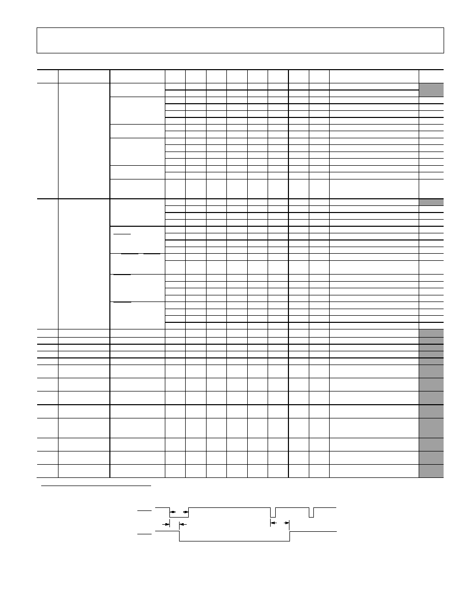
Preliminary Technical Data
ADV7322
Rev. PrA | Page 35 of 88
Table 17. Registers 0x4A to 0x58
SR7
SR0
Register
Bit Description
Bit 7
Bit 6
Bit 5
Bit 4
Bit 3
Bit 2
Bit 1
Bit 0
Register Setting
Reset
Value
0
Slave mode.
SD Slave/Master
Mode
1
Master
mode.
0x08
0
0
Mode
0.
0
1
Mode
1.
1
0
Mode
2.
SD Timing Mode
1
1
Mode
3.
0
Enabled.
SD BLANK Input
1
Disabled.
0
0
No delay.
0
1
2
clk
cycles.
1
0
4
clk
cycles.
SD Luma Delay
1
1
6
clk
cycles.
0
-40 IRE.
SD Min. Luma
Value
1
-7.5 IRE.
0x4A SD
Timing
Register 0
SD Timing Reset
x
0
0
0
0
0
0
0
A low-high-low transition will
reset the internal SD timing
counters.
0
0
T
a
= 1 clk cycle.
0x00
0
1
T
a
= 4 clk cycles.
1
0
T
a
= 16 clk cycles.
SD HSYNC Width
1
1
T
a
= 128 clk cycles.
0
0
T
b
= 0 clk cycle.
0
1
T
b
= 4 clk cycles.
1
0
T
b
= 8 clk cycles.
SD HSYNCto
VSYNC Delay
1
1
T
b
= 18 clk cycles.
x
0
T
c
= T
b
.
SD HSYNCto VSYNC
Rising Edge Delay
[Mode 1 Only]
x
1
T
c
= T
b
+ 32 µs.
0
0
1
clk
cycle.
0
1
4
clk
cycles.
1
0
16
clk
cycles.
VSYNC Width
[Mode 2 Only]
1
1
128
clk
cycles.
0
0
0
clk
cycles.
0
1
1
clk
cycle.
1
0
2
clk
cycles.
0x4B SD
Timing
Register 1
HSYNC to Pixel
Data Adjust
1
1
3
clk
cycles.
0x4C
SD F
SC
Register 0
1
x
x
x
x
x
x
x
x
Subcarrier Frequency Bits 70.
0x1E
1
0x4D SD
F
SC
Register 1
x
x
x
x
x
x
x
x
Subcarrier Frequency Bits 158.
0x7C
0x4E SD
F
SC
Register 2
x
x
x
x
x
x
x
x
Subcarrier Frequency Bits 2316.
0xF0
0x4F SD
F
SC
Register 3
x
x
x
x
x
x
x
x
Subcarrier Frequency Bits 3124.
0x21
0x50 SD
F
SC
Phase
x
x
x
x
x
x
x
x
Subcarrier Phase Bits 92.
0x00
0x51 SD
Closed
Captioning
Extended Data on
Even Fields
x
x
x
x
x
x
x
x
Extended Data Bits 70.
0x00
0x52 SD
Closed
Captioning
Extended Data on
Even Fields
x
x
x
x
x
x
x
x
Extended Data Bits 158.
0x00
0x53 SD
Closed
Captioning
Data on Odd Fields
x
x
x
x
x
x
x
x
Data Bits 70.
0x00
0x54 SD
Closed
Captioning
Data on Odd Fields
x
x
x
x
x
x
x
x
Data Bits 158.
0x00
0x55 SD
Pedestal
Register 0
Pedestal on Odd
Fields
17
16
15
14
13
12
11
10
Setting any of these bits to 1 will
disable pedestal on the line num-
ber indicated by the bit settings.
0x00
0x56 SD
Pedestal
Register 1
Pedestal on Odd
Fields
25
24
23
22
21
20
19
18
0x00
0x57 SD
Pedestal
Register 2
Pedestal on Even
Fields
17
16
15
14
13
12
11
10
0x00
0x58 SD
Pedestal
Register 3
Pedestal on Even
Fields
25
24
23
22
21
20
19
18
0x00
1
For precise NTSC FSC, this value should be programmed to 0x1F.
LINE 313
LINE 314
LINE 1
t
B
t
A
t
C
05067-
024
HSYNC
VSYNC
Figure 47. Timing Register 1 in PAL Mode
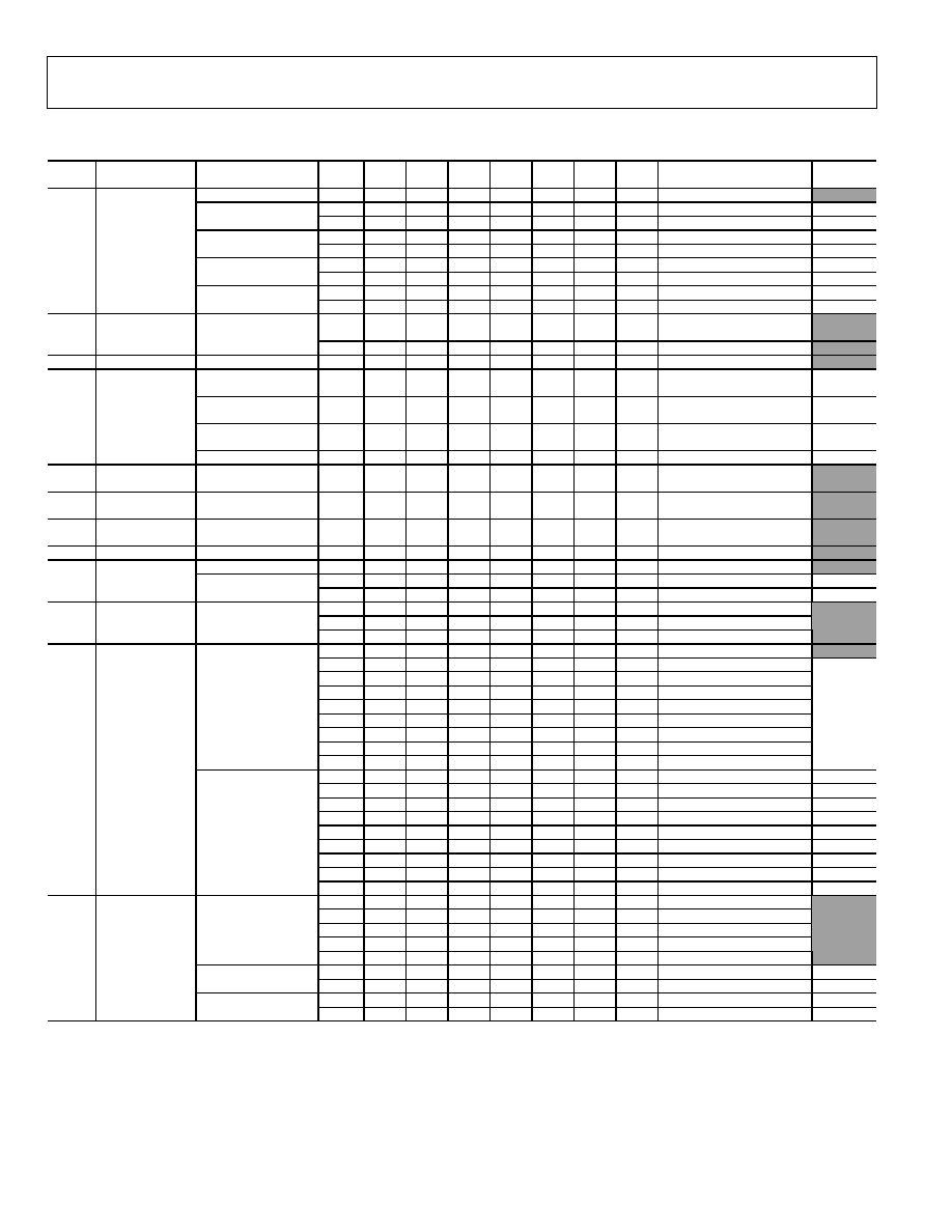
ADV7322
Preliminary Technical Data
Rev. PrA | Page 36 of 88
Table 18. Registers 0x59 to 0x64
SR7
SR0
Register
Bit Description
Bit 7
Bit 6
Bit 5
Bit 4
Bit 3
Bit 2
Bit 1
Bit 0
Register Setting
Reset
Values
SD CGMS Data
19
18
17
16
CGMS Data Bits C19C16
0x00
0
Disabled
SD CGMS CRC
1
Enabled
0
Disabled
SD CGMS on Odd
Fields
1
Enabled
0
Disabled
SD CGMS on Even
Fields
1
Enabled
0
Disabled
0x59
SD CGMS/WSS 0
SD WSS
1
Enabled
13
12
11
10
9
8
CGMS Data Bits C13C8, or
WSS Data Bits C13C8
0x00
0x5A
SD CGMS/WSS 1
SD CGMS/WSS Data
15
14
CGMS Data Bits C15C14
0x00
0x5B
SD CGMS/WSS 2
SD CGMS/WSS Data
7
6
5
4
3
2
1
0
CGMS/WSS Data Bits C7C0
0x00
SD LSB for Y Scale
Value
x
x
SD Y Scale Bits 10
SD LSB for Cb Scale
Value
x
x
SD Cb Scale Bits 10
SD LSB for Cr Scale
Value
x
x
SD Cr Scale Bits 10
0x5C
SD LSB Register
SD LSB for F
SC
Phase
x x Subcarrier
Phase
Bits
10
0x5D
SD Y Scale
Register
SD Y Scale Value
x
x
x
x
x
x
x
x
SD Y Scale Bits 72
0x00
0x5E
SD Cb Scale
Register
SD Cb Scale Value
x
x
x
x
x
x
x
x
SD Cb Scale Bits 72
0x00
0x5F
SD Cr Scale
Register
SD Cr Scale Value
x
x
x
x
x
x
x
x
SD Cr Scale Bits 72
0x00
0x60
SD Hue Register
SD Hue Adjust Value
x
x
x
x
x
x
x
x
SD Hue Adjust Bits 70
0x00
SD Brightness Value
x
x
x
x
x
x
x
SD Brightness Bits 60
0x00
0
Disabled
Line 23
0x61 SD
Brightness/
WSS
SD Blank WSS Data
1
Enabled
0
0
0
0
0
0
0
0
-4 dB
0
0
0
0
0
1
1
0
0 dB
0x62
SD Luma SSAF
SD Luma SSAF
Gain/Attenuation
0
0
0
0
1
1
0
0
+4 dB
0x00
0
0
0
0
No gain
0x00
0
0
0
1
+1/16 [1/8]
0
0
1
0
+2/16 [2/8]
0
0
1
1
+3/16 [3/8]
0
1
0
0
+4/16 [4/8]
0
1
0
1
+5/16 [5/8]
0
1
1
0
+6/16 [6/8]
0
1
1
1
+7/16 [7/8]
Coring Gain Border
1
0
0
0
+8/16 [1]
In DNR
mode,
the
values in
brackets
apply.
0
0
0
0
No gain
0
0
0
1
+1/16 [1/8]
0
0
1
0
+2/16 [2/8]
0
0
1
1
+3/16 [3/8]
0
1
0
0
+4/16 [4/8]
0
1
0
1
+5/16 [5/8]
0
1
1
0
+6/16 [6/8]
0
1
1
1
+7/16 [7/8]
0x63
SD DNR 0
Coring Gain Data
1
0
0
0
+8/16 [1]
0
0
0
0
0
0
0
0
0
0
0
0
1
1
...
...
...
...
...
...
...
1
1
1
1
1
0
62
DNR Threshold
1
1
1
1
1
1
63
0x00
0
2
pixels
Border Area
1
4
pixels
0
8
pixels
0x64
SD DNR 1
Block Size Control
1
16
pixels
Preliminary Technical Data
ADV7322
Rev. PrA | Page 37 of 88
Table 19. Registers 0x65 to 0x7C
SR7
SR0
Register
Bit Description
Bit 7
Bit 6
Bit 5
Bit 4
Bit 3
Bit 2
Bit 1
Bit 0
Register Setting
Reset
Values
0
0
1
Filter
A
0
1
0
Filter B
0
1
1
Filter
C
DNR Input Select
1
0
0
Filter D
0x00
0
DNR
mode
DNR Mode
1
DNR
sharpness
mode
0
0
0
0
0 pixel offset
0
0
0
1
1 pixel offset
...
...
...
...
...
1
1
1
0
14 pixel offset
0x65
SD DNR 2
DNR Block Offset
1
1
1
1
15 pixel offset
0x66
SD Gamma A
SD Gamma Curve A Data Points
x
x
x
x
x
x
x
x
A0
0x00
0x67
SD Gamma A
SD Gamma Curve A Data Points
x
x
x
x
x
x
x
x
A1
0x00
0x68
SD Gamma A
SD Gamma Curve A Data Points
x
x
x
x
x
x
x
x
A2
0x00
0x69
SD Gamma A
SD Gamma Curve A Data Points
x
x
x
x
x
x
x
x
A3
0x00
0x6A
SD Gamma A
SD Gamma Curve A Data Points
x
x
x
x
x
x
x
x
A4
0x00
0x6B
SD Gamma A
SD Gamma Curve A Data Points
x
x
x
x
x
x
x
x
A5
0x00
0x6C
SD Gamma A
SD Gamma Curve A Data Points
x
x
x
x
x
x
x
x
A6
0x00
0x6D
SD Gamma A
SD Gamma Curve A Data Points
x
x
x
x
x
x
x
x
A7
0x00
0x6E
SD Gamma A
SD Gamma Curve A Data Points
x
x
x
x
x
x
x
x
A8
0x00
0x6F
SD Gamma A
SD Gamma Curve A Data Points
x
x
x
x
x
x
x
x
A9
0x00
0x70
SD Gamma B
SD Gamma Curve B Data Points
x
x
x
x
x
x
x
x
B0
0x00
0x71
SD Gamma B
SD Gamma Curve B Data Points
x
x
x
x
x
x
x
x
B1
0x00
0x72
SD Gamma B
SD Gamma Curve B Data Points
x
x
x
x
x
x
x
x
B2
0x00
0x73
SD Gamma B
SD Gamma Curve B Data Points
x
x
x
x
x
x
x
x
B3
0x00
0x74
SD Gamma B
SD Gamma Curve B Data Points
x
x
x
x
x
x
x
x
B4
0x00
0x75
SD Gamma B
SD Gamma Curve B Data Points
x
x
x
x
x
x
x
x
B5
0x00
0x76
SD Gamma B
SD Gamma Curve B Data Points
x
x
x
x
x
x
x
x
B6
0x00
0x77
SD Gamma B
SD Gamma Curve B Data Points
x
x
x
x
x
x
x
x
B7
0x00
0x78
SD Gamma B
SD Gamma Curve B Data Points
x
x
x
x
x
x
x
x
B8
0x00
0x79
SD Gamma B
SD Gamma Curve B Data Points
x
x
x
x
x
x
x
x
B9
0x00
0x7A
SD Brightness
Detect
SD Brightness Value
x
x
x
x
x
x
x
x
Read only
Field Count
x
x
x
Read only
0x8x
Reserved
0
Reserved
Reserved
0
Reserved
Reserved
0
Reserved
0x7B
Field Count
Register
Revision Code
1
0
Read only
0x7C
Reserved
Reserved
0x00
ADV7322
Preliminary Technical Data
Rev. PrA | Page 38 of 88
Table 20. Registers 0x7D to 0x91
SR7-
SR0
Register
Bit
Description
Bit 7
Bit 6
Bit 5
Bit 4
Bit 3
Bit 2
Bit 1
Bit 0
Register
Setting
Reset
Values
0x7D
Reserved
0x7E
Reserved
0x7F
Reserved
0x80
Macrovision
MV Control Bits
x
x
x
x
x
x
x
x
0x00
0x81
Macrovision
MV Control Bits
x
x
x
x
x
x
x
x
0x00
0x82
Macrovision
MV Control Bits
x
x
x
x
x
x
x
x
0x00
0x83
Macrovision
MV Control Bits
x
x
x
x
x
x
x
x
0x00
0x84
Macrovision
MV Control Bits
x
x
x
x
x
x
x
x
0x00
0x85
Macrovision
MV Control Bits
x
x
x
x
x
x
x
x
0x00
0x86
Macrovision
MV Control Bits
x
x
x
x
x
x
x
x
0x00
0x87
Macrovision
MV Control Bits
x
x
x
x
x
x
x
x
0x00
0x88
Macrovision
MV Control Bits
x
x
x
x
x
x
x
x
0x00
0x89
Macrovision
MV Control Bits
x
x
x
x
x
x
x
x
0x00
0x8A
Macrovision
MV Control Bits
x
x
x
x
x
x
x
x
0x00
0x8B
Macrovision
MV Control Bits
x
x
x
x
x
x
x
x
0x00
0x8C
Macrovision
MV Control Bits
x
x
x
x
x
x
x
x
0x00
0x8D
Macrovision
MV Control Bits
x
x
x
x
x
x
x
x
0x00
0x8E
Macrovision
MV Control Bits
x
x
x
x
x
x
x
x
0x00
0x8F
Macrovision
MV Control Bits
x
x
x
x
x
x
x
x
0x00
0x90
Macrovision
MV Control Bits
x
x
x
x
x
x
x
x
0x00
0x91
Macrovision
MV Control Bit
0
0
0
0
0
0
0
x
0 must be written
to these bits
0x00
Preliminary Technical Data
ADV7322
Rev. PrA | Page 39 of 88
INPUT CONFIGURATION
Note that the ADV7322 defaults to simultaneous standard
definition and progressive scan upon power-up (Address[0x01]:
Input Mode = 011).
STANDARD DEFINITION ONLY
Address[0x01]: Input Mode = 000
The 8-bit multiplexed input data is input on Pins S7 to S0 (or
Pins Y7 to Y0, depending on Register Address 0x01, Bit 7), with
S0 being the LSB in 8-bit input mode (see Table 21). Input
standards supported are ITU-R BT.601/656. In 16-bit input
mode, the Y pixel data is input on Pins S7 to S0 and CrCb data
is input on Pins Y7 to Y0 (see Table 21).
16-Bit Mode Operation
When Register 0x01 Bit 7 = 0, CrCb data is input on the Y bus
and Y data is input on the S bus. When Register 0x01 Bit 7 = 1,
CrCb data is input on the C bus and Y data is input on Y bus.
The 27 MHz clock input must be input on Pin CLKIN_A. Input
sync signals are input on the S_VSYNC, S_HSYNC, and
S_BLANK pins.
Table 21. SD 8-Bit and 16-Bit Configuration
Configuration
Parameter
8-Bit Mode
16-Bit Mode
Register 0x01, Bit 7 = 0
Y Bus
CrCb
S Bus
656/601, YCrCb
Y
C Bus
Register 0x01, Bit 7 = 1
Y Bus
656/601, YCrCb
Y
S Bus
C Bus
CrCb
MPEG2
DECODER
CLKIN_A
S[7:0] OR Y[7:0]*
27MHz
3
8
YCrCb
ADV7322
*SELECTED BY ADDRESS 0x01 BIT 7
05067-
025
S_VSYNC,
S_HSYNC,
S_BLANK
Figure 48. SD Only Input Mode
PROGRESSIVE SCAN ONLY OR HDTV ONLY
Address[0x01]: Input Mode = 001 or 010, Respectively
YCrCb progressive scan, HDTV, or any other HD YCrCb data
can be input in 4:2:2 or 4:4:4. In 4:2:2 input mode, the Y data is
input on Pins Y7 to Y0 and the CrCb data is input on Pins C7 to
C0. In 4:4:4 input mode, Y data is input on Pins Y7 to Y0,
Cb data is input on Pins C7 to C0, and Cr data is input on Pins
S7 to S0. If the YCrCb data does not conform to SMPTE 293M
(525p), ITU-R BT.1358M (625p), SMPTE 274M[1080i], SMPTE
296M[720p], SMPTE 240M(1035i) or BTA-T1004/1362, the
async timing mode must be used. RGB data can only be input in
4:4:4 format in PS input mode or in HDTV input mode when
HD RGB input is enabled. G data is input on Pins Y7 to Y0, R
data is input on Pins S7 to S0, and B data is input on Pins C7 to
C0. The clock signal must be input on Pin CLKIN_A.
MPEG2
DECODER
CLKIN_A
C[7:0]
8
Cb
S[7:0]
Y[7:0]
INTERLACED TO
PROGRESSIVE
YCrCb
8
Cr
8
Y
3
27MHz
ADV7322
05067-
026
P_VSYNC,
P_HSYNC,
P_BLANK
Figure 49. Progressive Scan Input Mode
SIMULTANEOUS STANDARD DEFINITION AND
PROGRESSIVE SCAN OR HDTV
Address[0x01]: Input Mode 011 (SD 8-Bit, PS 16-Bit) or 101
(SD and HD, SD Oversampled), 110 (SD and HD, HD
Oversampled), Respectively
YCrCb, PS, HDTV, or any other HD data must be input in 4:2:2
format. In 4:2:2 input mode, the HD Y data is input on Pins Y7
to Y0 and the HD CrCb data is input on Pins C7 to C0. If PS
4:2:2 data is interleaved onto a single 10-bit bus, Pins Y7 to Y0
are used for the input port. The input data is to be input at 27
MHz, with the data being clocked on the rising and falling edge
of the input clock. The input mode register at Address 0x01 is
set accordingly. If the YCrCb data does not conform to SMPTE
293M (525p), ITU-R BT.1358M (625p), SMPTE 274M[1080i],
SMPTE 296M[720p], SMPTE 240M(1035i) or BTA-T1004, the
async timing mode must be used.
The 8- bit standard definition data must be compliant with
ITU-R BT.601/656 in 4:2:2 format. Standard definition data is
input on Pins S7 to S0, with S0 being the LSB. The clock input
for SD must be input on CLKIN_A and the clock input for
HD/PS must be input on CLKIN_B. Synchronization signals
are optional. SD syncs are input on Pins S_VSYNC, S_HSYNC,
and S_BLANK. HD syncs on Pins P_VSYNC, P_HSYNC, and
P_BLANK.
ADV7322
Preliminary Technical Data
Rev. PrA | Page 40 of 88
CLKIN_A
CLKIN_B
MPEG2
DECODER
3
27MHz
8
YCrCb
INTERLACED TO
PROGRESSIVE
8
CrCb
8
Y
3
27MHz
S[7:0]
C[7:0]
Y[7:0]
ADV7322
05067-
027
S_VSYNC,
S_HSYNC,
S_BLANK
P_VSYNC,
P_HSYNC,
P_BLANK
Figure 50. Simultaneous PS and SD Input
CLKIN_A
CLKIN_B
SDTV
DECODER
3
27MHz
8
YCrCb
8
CrCb
8
Y
3
74.25MHz
1080i
OR
720p
OR
1035i
S[7:0]
C[7:0]
Y[7:0]
ADV7322
HDTV
DECODER
05067-
028
S_VSYNC,
S_HSYNC,
S_BLANK
P_VSYNC,
P_HSYNC,
P_BLANK
Figure 51. Simultaneous HD and SD Input
If in simultaneous SD/HD input mode and the two clock phases
differ by less than 9.25 ns or more than 27.75 ns, the CLOCK
ALIGN bit [Address 0x01, Bit 3] must be set accordingly. If the
application uses the same clock source for both SD and PS, the
CLOCK ALIGN bit must be set since the phase difference
between both inputs is less than 9.25 ns.
CLKIN_A
CLKIN_B
05067-029
t
DELAY
<
9.25ns OR
t
DELAY
>
27.75ns
Figure 52. Clock Phase with Two Input Clocks
PROGRESSIVE SCAN AT 27 MHZ (DUAL EDGE)
OR 54 MHZ
Address[0x01]: Input Mode 100 or 111, Respectively
YCrCb progressive scan data can be input at 27 MHz or
54 MHz. The input data is interleaved onto a single 8-bit bus
and is input on Pins Y7 to Y0. When a 27 MHz clock is supplied,
the data is clocked in on the rising and falling edge of the input
clock and CLOCK EDGE [Address 0x01, Bit 1] must be set
accordingly.
Table 22 provides an overview of all possible input configurations.
Figure 53, Figure 54, and Figure 55 show the possible conditions:
(a) Cb data on the rising edge; and (b) Y data on the rising edge.
FF
00
00
XY
Y0
Y1
Cr0
CLKIN_B
CLOCK EDGE ADDRESS 0x00 BIT 1 SHOULD BE SET TO 0 IN THIS CASE.
Y7Y0
Cb0
05067-
030
Figure 53. Input Sequence in PS Bit Interleaved Mode (EAV/SAV)
FF
00
00
XY
Cb0
Cr0
Y1
CLKIN_B
Y7Y0
Y0
CLOCK EDGE ADDRESS 0x00 BIT 1 SHOULD BE SET TO 1 IN THIS CASE.
05067-
031
Figure 54. Input Sequence in PS Bit Interleaved Mode (EAV/SAV)
PIXEL INPUT
DATA
FF
00
00
XY
Cb0
Y0
Y1
Cr0
CLKIN_B
WITH A 54MHz CLOCK, THE DATA IS LATCHED ON EVERY RISING EDGE.
05067-
032
Figure 55. Input Sequence in PS Bit Interleaved Mode (EAV/SAV)
MPEG2
DECODER
CLKIN_A
Y[7:0]
INTERLACED
TO
PROGRESSIVE
YCrCb
8
3
27MHz OR 54MHz
YCrCb
ADV7322
P_VSYNC,
P_HSYNC,
P_BLANK
05067-
033
Figure 56. 10-Bit PS at 27 MHz or 54 MHz
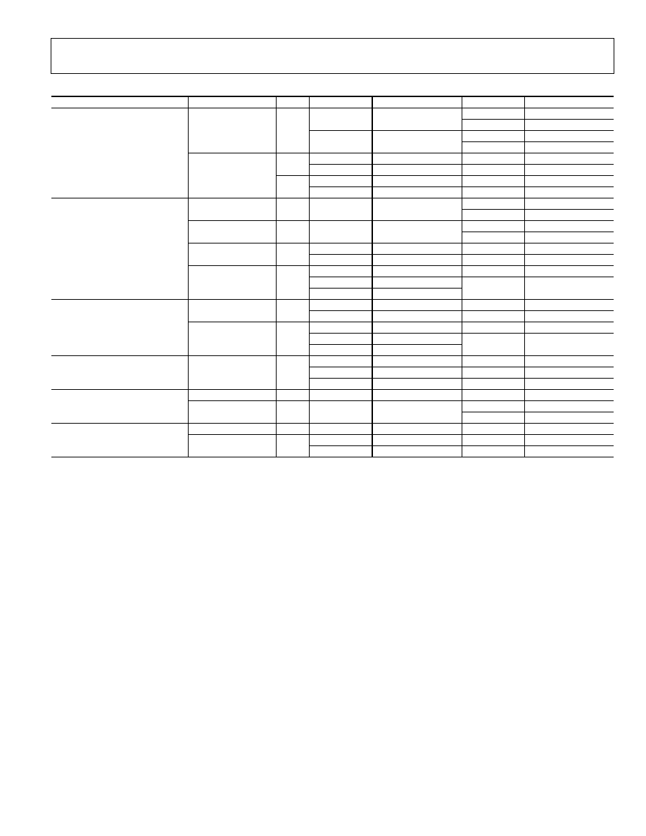
Preliminary Technical Data
ADV7322
Rev. PrA | Page 41 of 88
Table 22. Input Configurations
Input Format
Total Bits
Input Video
Input Pins
Subaddress
Register Setting
0x01 0x00
YCrCb
S7S0 [MSB = S7]
0x48 0x00
0x01 0x80
8
4:2:2
YCrCb
Y7Y0 [MSB = Y7]
0x48 0x00
Y
S7S0 [MSB = S7]
0x01
0x00
4:2:2
CrCb
Y7Y20[MSB = Y7]
0x48
0x08
Y
Y7Y0 [MSB = Y7]
0x01
0x80
ITU-R BT.656
(4 options available)
See Table 21
16
4:2:2
CrCb
C7C0 [MSB = Y7]
0x48
0x00
0x01 0x10
8 [27 MHz clock]
4:2:2
YCrCb
Y7Y0 [MSB = Y7]
0x13 0x40
0x01 0x70
8 [54 MHz clock]
4:2:2
YCrCb
Y7Y0 [MSB = Y7]
0x13 0x40
Y
Y7Y0 [MSB = Y7]
0x01
0x10
16
4:2:2
CrCb
C7C0 [MSB = C7]
0x13
0x40
Y
Y7Y0 [MSB = Y7]
0x01
0x10
Cb
C7C0 [MSB = C7]
PS Only
24
4:4:4
Cr
S7S0 [MSB = S7]
0x13 0x00
Y
Y7Y0 [MSB = Y7]
0x01
0x20
16
4:2:2
CrCb
C7C0 [MSB = C7]
0x13
0x40
Y
Y7Y0 [MSB = Y7]
0x01
0x20
Cb
C7C0 [MSB = C7]
HDTV Only
24
4:4:4
Cr
S7S0 [MSB = S7]
0x13 0x00
G
Y7Y0 [MSB = Y7]
0x01
0x10 or 0x20
B
C7C0 [MSB = C7]
0x13
0x00
HD RGB
24
4:4:4
R
S7S0 [MSB = S7]
0x15
0x02
8 (SD)
4:2:2
YCrCb
S7S0 [MSB = S7]
0x01
0x40
0x13 0x40
ITU-R BT.656 and PS
8 (PS)
4:2:2
YCrCb
Y7Y0 [MSB = Y7]
0x48 0x00
8
4:2:2
YCrCb
S7S0 [MSB = S7]
0x01
0x30, 0x50, or 0x60
Y
Y7Y0 [MSB = Y7]
0x13
0x40
ITU-R BT.656 and PS or HDTV
16
4:2:2
CrCb
C7C0 [MSB = C7]
0x48
0x00
ADV7322
Preliminary Technical Data
Rev. PrA | Page 42 of 88
FEATURES
OUTPUT CONFIGURATION
Table 23, Table 24, and Table 25 demonstrate what output signals are assigned to the DACs when the control bits are set accordingly.
Table 23. Output Configuration in SD Only Mode
RGB/YUV Output
0x02, Bit 5
SD DAC Output 1
0x42, Bit 2
SD DAC Output 2
0x42, Bit 1
DAC A
DAC B
DAC C
DAC D
DAC E
DAC F
0
0
0
CVBS
Luma
Chroma
G
B
R
0
0
1
G
B
R
CVBS
Luma
Chroma
0
1
0
G
Luma
Chroma
CVBS
B
R
0
1
1
CVBS
B
R
G
Luma
Chroma
1
0
0
CVBS
Luma
Chroma
Y
U
V
1
0
1
Y
U
V
CVBS
Luma
Chroma
1
1
0
Y
Luma
Chroma
CVBS
U
V
1
1
1
CVBS
U
V
Y
Luma
Chroma
Luma/Chroma Swap 0x44, Bit 7
0 Table as above
1 Table above with all luma/chroma instances swapped
Table 24. Output Configuration in HD/PS Only Mode
HD/PS
Input Format
HD/PS RGB Input
0x15, Bit 1
RGB/YPrPb Output
0x02, Bit 5
HD/PS Color
Swap 0x15, Bit 3
DAC A
DAC B
DAC C DAC D DAC E
DAC F
YCrCb 4:2:2
0
0
0
N/A
N/A
N/A
G
B
R
YCrCb 4:2:2
0
0
1
N/A
N/A
N/A
G
R
B
YCrCb 4:2:2
0
1
0
N/A
N/A
N/A
Y
Pb
Pr
YCrCb 4:2:2
0
1
1
N/A
N/A
N/A
Y
Pr
Pb
YCrCb 4:4:4
0
0
0
N/A
N/A
N/A
G
B
R
YCrCb 4:4:4
0
0
1
N/A
N/A
N/A
G
R
B
YCrCb 4:4:4
0
1
0
N/A
N/A
N/A
Y
Pb
Pr
YCrCb 4:4:4
0
1
1
N/A
N/A
N/A
Y
Pr
Pb
RGB 4:4:4
1
0
0
N/A
N/A
N/A
G
B
R
RGB 4:4:4
1
0
1
N/A
N/A
N/A
G
R
B
RGB 4:4:4
1
1
0
N/A
N/A
N/A
G
B
R
RGB 4:4:4
1
1
1
N/A
N/A
N/A
G
R
B
Table 25. Output Configuration in Simultaneous SD and HD/PS Only Mode
Input Formats
RGB/YPrPb Output
0x02, Bit 5
HD/PS Color Swap
0x15, Bit 3
DAC A
DAC B
DAC C
DAC D
DAC E
DAC F
ITU-R.BT656 and HD
YCrCb in 4:2:2
0
0
CVBS
Luma
Chroma
G
B
R
ITU-R.BT656 and HD
YCrCb in 4:2:2
0
1
CVBS
Luma
Chroma
G
R
B
ITU-R.BT656 and HD
YCrCb in 4:2:2
1
0
CVBS
Luma
Chroma
Y
Pb
Pr
ITU-R.BT656 and HD
YCrCb in 4:2:2
1
1
CVBS
Luma
Chroma
Y
Pr
Pb
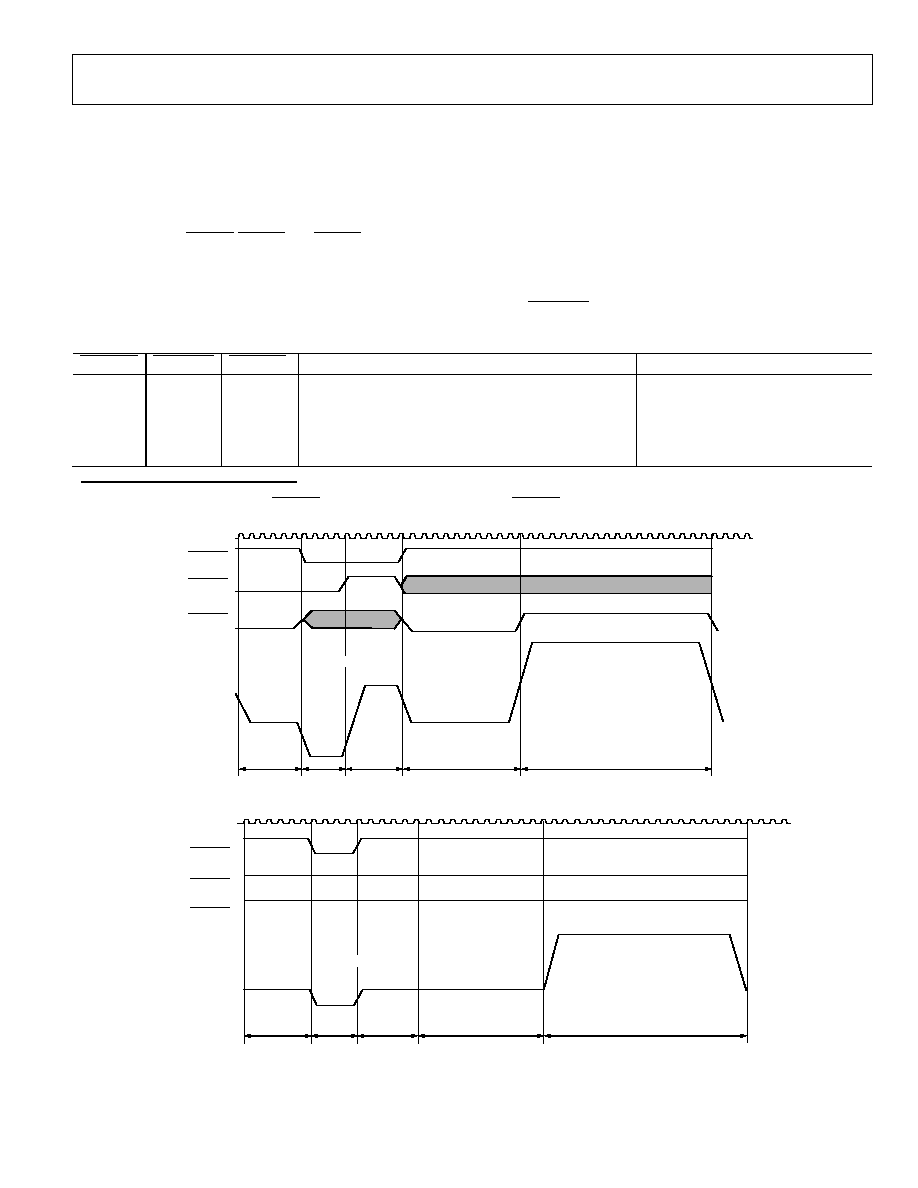
Preliminary Technical Data
ADV7322
Rev. PrA | Page 43 of 88
HD ASYNC TIMING MODE
[Subaddress 0x10, Bits 3 and 2]
For any input data that does not conform to the standards
selectable in input mode, Subaddress 0x10, asynchronous
timing mode can be used to interface to the ADV7322. Timing
control signals for HSYNC, VSYNC, and BLANK must be
programmed by the user. Macrovision and programmable
oversampling rates are not available in async timing mode.
In async mode, the PLL must be turned off [Subaddress 0x00,
Bit 1 = 1]. Register 0x10 should be programmed to 0x01.
Figure 57 and Figure 58 show examples of how to program the
ADV7322 to accept a high definition standard other than
SMPTE 293M, SMPTE 274M, SMPTE 296M, or ITU-R
BT.1358.
Table 26 must be followed when programming the control signals
in async timing mode. For standards that do not require a trisync
level, P_BLANK must be tied low at all times.
Table 26. Async Timing Mode Truth Table
P_HSYNC P_VSYNC P_BLANK
1
Reference
Reference in Figure 57 and Figure 58
1 --> 0
0
0 or 1
50% point of falling edge of trilevel horizontal sync signal
a
0
0 --> 1
0 or 1
25% point of rising edge of trilevel horizontal sync signal
b
0 --> 1
0 or 1
0
50% point of falling edge of trilevel horizontal sync signal
c
1
0 or 1
0 --> 1
50% start of active video
d
1
0 or 1
1 --> 0
50% end of active video
e
1
When async timing mode is enabled, P_BLANK, Pin 25, becomes an active high input. P_BLANK is set to active low at Address 0x10, Bit 6.
CLK
ACTIVE VIDEO
PROGRAMMABLE
INPUT TIMING
ANALOG
OUTPUT
81
66
66
243
1920
HORIZONTAL SYNC
e
d
c
b
a
SET ADDRESS 0x14,
BIT 3 = 1
05067-034
P_HSYNC
P_VSYNC
P_BLANK
Figure 57. Async Timing Mode--Programming Input Control Signals for SMPTE 295M Compatibility
ACTIVE VIDEO
0
1
HORIZONTAL SYNC
e
d
c
b
a
CLK
SET ADDRESS 0x14
BIT 3 = 1
ANALOG OUTPUT
05067-035
P_VSYNC
P_BLANK
P_HSYNC
Figure 58. Async Timing Mode--Programming Input Control Signals for Bilevel Sync Signal
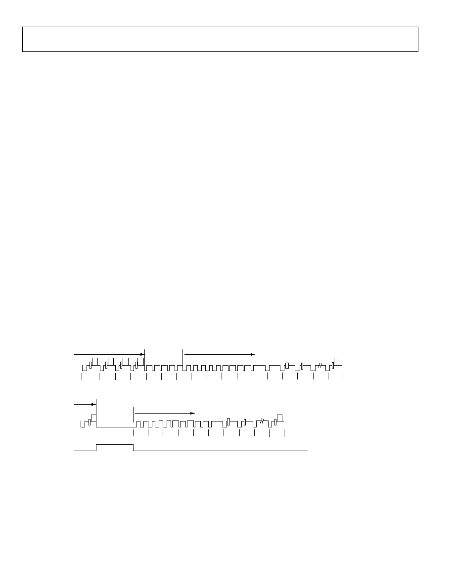
ADV7322
Preliminary Technical Data
Rev. PrA | Page 44 of 88
HD TIMING RESET
A timing reset is achieved by toggling the HD timing reset control
bit [Subaddress 0x14, Bit 0] from 0 to 1. In this state the horizontal
and vertical counters will remain reset. When this bit is set back to
0, the internal counters will commence counting again.
The minimum time the pin has to be held high is one clock
cycle; otherwise, this reset signal might not be recognized. This
timing reset applies to the HD timing counters only.
SD REAL-TIME CONTROL, SUBCARRIER RESET,
AND TIMING RESET
[Subaddress 0x44, Bits 2 and 1]
Together with the RTC_SCR_TR pin and SD Mode Register 3
[Address 0x44, Bits 1 and 2], the ADV7322 can be used in (a)
timing reset mode, (b) subcarrier phase reset mode, or (c) RTC
mode.
a.
A timing reset is achieved in a low-to-high transition
on the RTC_SCR_TR pin (Pin 31). In this state, the
horizontal and vertical counters will remain reset.
Upon releasing this pin (set to low), the internal
counters will commence counting again, the field
count will start on Field 1, and the subcarrier phase
will be reset.
The minimum time the pin must be held high is one
clock cycle; otherwise, this reset signal might not be
recognized. This timing reset applies to the SD timing
counters only.
b.
In subcarrier phase reset, a low-to-high transition on
the RTC_SCR_TR pin (Pin 31) will reset the
subcarrier phase to zero on the field following the
subcarrier phase reset when the SD RTC/TR/SCR
control bits at Address 0x44 are set to 01.
This reset signal must be held high for a minimum of
one clock cycle.
Since the field counter is not reset, it is recommended
that the reset signal is applied in Field 7 [PAL] or Field
3 [NTSC]. The reset of the phase will then occur on
the next field, i.e., Field 1, being lined up correctly with
the internal counters. The field count register at
Address 0x7B can be used to identify the number of
the active field.
c.
In RTC mode, the ADV7322 can be used to lock to an
external video source. The real-time control mode
allows the ADV7322 to automatically alter the
subcarrier frequency to compensate for line length
variations. When the part is connected to a device that
outputs a digital data stream in the RTC format, such
as an ADV7183A video decoder (see Figure 61), the
part will automatically change to the compensated
subcarrier frequency on a line by line basis. This
digital data stream is 67 bits wide and the subcarrier is
contained in Bits 0 to 21. Each bit is two clock cycles
long. Write 0x00 into all four subcarrier frequency
registers when this mode is used.
DISPLAY
NO TIMING RESET APPLIED
TIMING RESET APPLIED
START OF FIELD 4 OR 8
F
SC
PHASE = FIELD 4 OR 8
F
SC
PHASE = FIELD 1
TIMING RESET PULSE
307
310
307
1
2
3
4
5
6
7
21
313
320
DISPLAY
START OF FIELD 1
05067-036
Figure 59. Timing Reset Timing Diagram
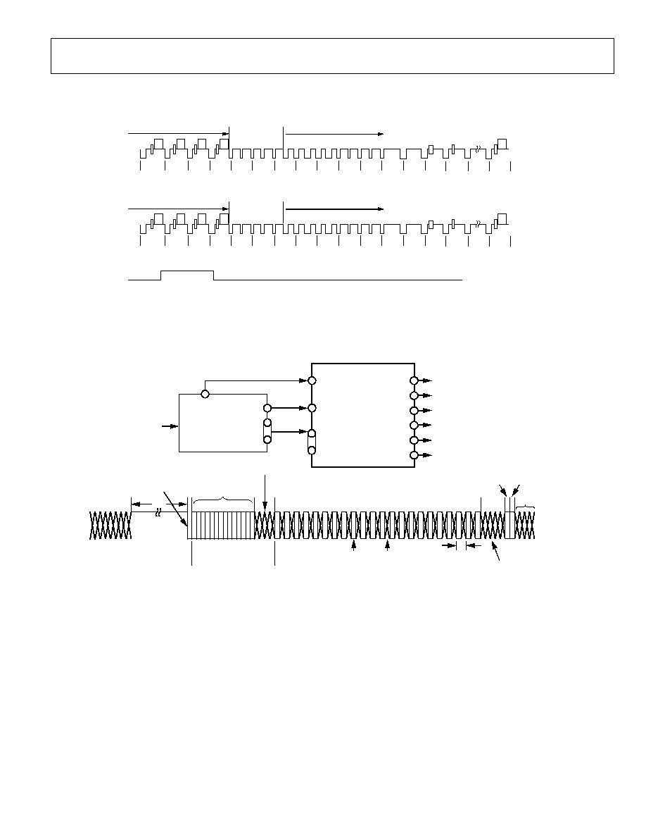
Preliminary Technical Data
ADV7322
Rev. PrA | Page 45 of 88
NO F
SC
RESET APPLIED
F
SC
PHASE = FIELD 4 OR 8
307
310
313
320
DISPLAY
START OF FIELD 4 OR 8
F
SC
RESET APPLIED
F
SC
RESET PULSE
F
SC
PHASE = FIELD 1
307
310
313
320
DISPLAY
START OF FIELD 4 OR 8
05067-037
Figure 60. Subcarrier Reset Timing Diagram
LCC1
GLL
P17P10
ADV7183A
VIDEO
DECODER
COMPOSITE
VIDEO
1
CLKIN_A
RTC_SCR_TR
DAC A
DAC B
DAC C
DAC D
DAC E
DAC F
Y7Y0/S7S0
5
RTC
LOW
H/L TRANSITION
COUNT START
128
TIME SLOT 01
13
0
14 BITS
SUBCARRIER
PHASE
14
21
19
F
SC
PLL INCREMENT
2
VALID
SAMPLE
INVALID
SAMPLE
6768
4 BITS
RESERVED
0
SEQUENCE
BIT
3
RESET
BIT
4
RESERVED
ADV7322
NOTES
1
i.e., VCR OR CABLE
2
F
SC
PLL INCREMENT IS 22 BITS LONG. VALUE LOADED INTO ADV7322 F
SC
DDS REGISTER IS F
SC
PLL INCREMENTS BITS 21:0
PLUS BITS 0:9 OF SUBCARRIER FREQUENCY REGISTERS. ALL ZEROS SHOULD BE WRITTEN TO THE SUBCARRIER FREQUENCY REGISTERS
OF THE ADV7322.
3
SEQUENCE BIT
PAL: 0 = LINE NORMAL, 1 = LINE INVERTED
NTSC: 0 = NO CHANGE
4
RESET ADV7322 DDS
5
SELECTED BY REGISTER ADDRESS 0x01 BIT 7
05067-
038
8/LINE
LOCKED
CLOCK
5 BITS
RESERVED
Figure 61. RTC Timing and Connections
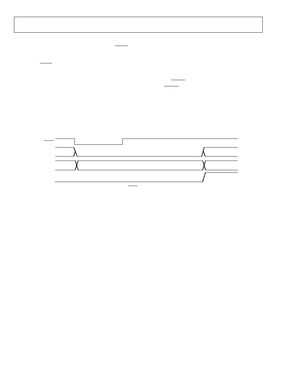
ADV7322
Preliminary Technical Data
Rev. PrA | Page 46 of 88
RESET SEQUENCE
A reset is activated with a high-to-low transition on the RESET
pin [Pin 33] according to the timing specifications. The
ADV7322 will revert to the default output configuration. Figure 62
illustrates the RESET timing sequence.
SD VCR FF/RW SYNC
[Subaddress 0x42, Bit 5]
In DVD record applications where the encoder is used with a
decoder, the VCR FF/RW sync control bit can be used for
nonstandard input video, i.e., in fast forward or rewind modes.
In fast forward mode, the sync information at the start of a new
field in the incoming video usually occurs before the correct
number of lines/fields is reached; in rewind mode, this sync
signal usually occurs after the total number of lines/fields is
reached. Conventionally this means that the output video will
have corrupted field signals, one generated by the incoming
video and one generated when the internal lines/field counters
reach the end of a field.
When the VCR FF/RW sync control is enabled [Subaddress
0x42, Bit 5], the lines/fields counters are updated according to
the incoming VSYNC signal, and the analog output matches the
incoming VSYNC signal.
This control is available in all slave timing modes except Slave
Mode 0.
XXXXXX
XXXXXX
OFF
DIGITAL TIMING SIGNALS SUPPRESSED
VALID VIDEO
TIMING ACTIVE
RESET
DIGITAL TIMING
DACs
A, B, C
PIXEL DATA
VALID
05067-039
Figure 62. RESET Timing Sequence

Preliminary Technical Data
ADV7322
Rev. PrA | Page 47 of 88
VERTICAL BLANKING INTERVAL
The ADV7322 accepts input data that contains VBI data
[CGMS, WSS, VITS, and so on] in SD and HD modes.
For SMPTE 293M [525p] standards, VBI data can be inserted
on Lines 13 to 42 of each frame, or on Lines 6 to 43 for the
ITU-R BT.1358 [625p] standard.
For SD NTSC this data can be present on Lines 10 to 20, and in
PAL on Lines 7 to 22.
If VBI is disabled [Address 0x11, Bit 4 for HD; Address 0x43,
Bit 4 for SD], VBI data is not present at the output and the
entire VBI is blanked. These control bits are valid in all master
and slave modes.
In Slave Mode 0, if VBI is enabled, the blanking bit in the
EAV/SAV code is overwritten. It is possible to use VBI in this
timing mode as well.
In Slave Mode 1 or 2, the BLANK control bit must be set to
enabled [Address 0x4A, Bit 3] to allow VBI data to pass through
the ADV7322. Otherwise, the ADV7322 automatically blanks
the VBI to standard.
If CGMS is enabled and VBI is disabled, the CGMS data will
nevertheless be available at the output.
See Appendix 1--Copy Generation Management System.
SUBCARRIER FREQUENCY REGISTERS
[Subaddresses 0x4C to 0x4F]
Four 8-bit registers are used to set up the subcarrier frequency.
The value of these registers is calculated using the equation
32
2
27
×
=
line
video
one
in
cycles
clk
MHz
of
Number
line
video
one
in
periods
subcarrier
of
Number
Register
Frequency
Subcarrier
where the sum is rounded to the nearest integer.
For example, in NTSC mode
569408543
2
1716
5
.
227
Re
32
=
×
=
Value
gister
Subcarrier
where:
Subcarrier Register Value
= 0x21F07C1F
SD F
SC
Register 0: 0x1F
SD F
SC
Register 1: 0x7C
SD F
SC
Register 2: 0xF0
SD F
SC
Register 3: 0x21
See the MPU Port Description section for more details on how
to access the subcarrier frequency registers.
Programming the F
SC
The Subcarrier Register Value is shared across 4 F
SC
registers as
shown above. To load the value into the encoder, users must
write to the F
SC
registers in sequence, starting with F
SC
0. The
value is not loaded until the F
SC
4 write is complete.
Note that the ADV7322 power-up value for F
SC
0 = 0x1E. For
precise NTSC F
SC
, write 0x1F to this register.
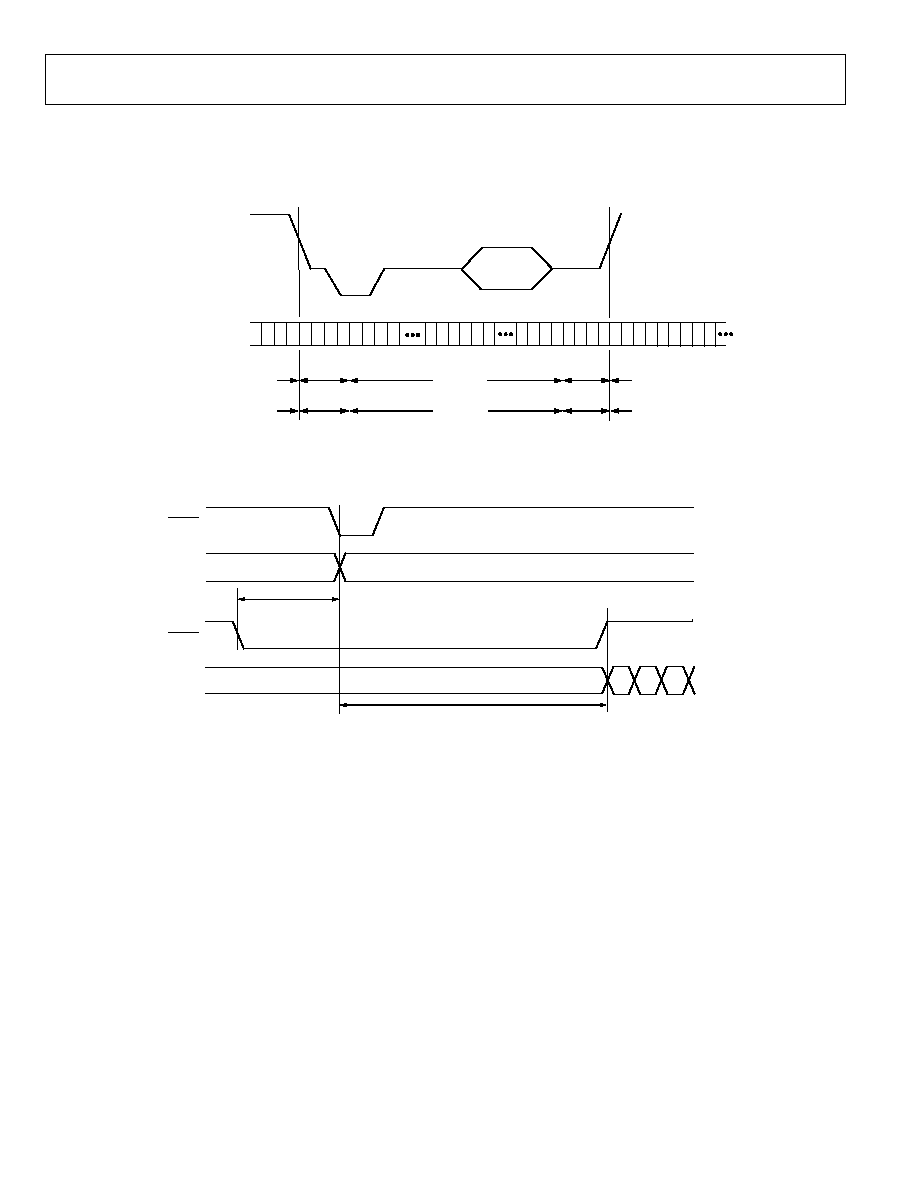
ADV7322
Preliminary Technical Data
Rev. PrA | Page 48 of 88
SQUARE PIXEL TIMING MODE
[Address 0x42, Bit 4]
In square pixel mode, the following timing diagrams apply.
Y Cr Y
F
F
0
0
0
0
X
Y
8
0
1
0
8
0
1
0
F
F
0
0
F
F
A
B
A
B
A
B
8
0
1
0
8
0
1
0
F
F
0
0
0
0
X
Y
C
b
Y C
r
C
b
Y
C
b
Y
C
r
EAV CODE
SAV CODE
ANCILLARY DATA
(HANC)
4 CLOCK
4 CLOCK
272 CLOCK
1280 CLOCK
4 CLOCK
4 CLOCK
344 CLOCK
1536 CLOCK
END OF ACTIVE
VIDEO LINE
START OF ACTIVE
VIDEO LINE
ANALOG
VIDEO
INPUT PIXELS
NTSC/PAL M SYSTEM
(525 LINES/60Hz)
PAL SYSTEM
(625 LINES/50Hz)
Y
05067-040
Figure 63. EAV/SAV Embedded Timing
FIELD
PIXEL
DATA
PAL = 44 CLOCK CYCLES
NTSC = 44 CLOCK CYCLES
PAL = 136 CLOCK CYCLES
NTSC = 208 CLOCK CYCLES
Cb
Y
Cr
Y
05067-041
HSYNC
BLANK
Figure 64. Active Pixel Timing
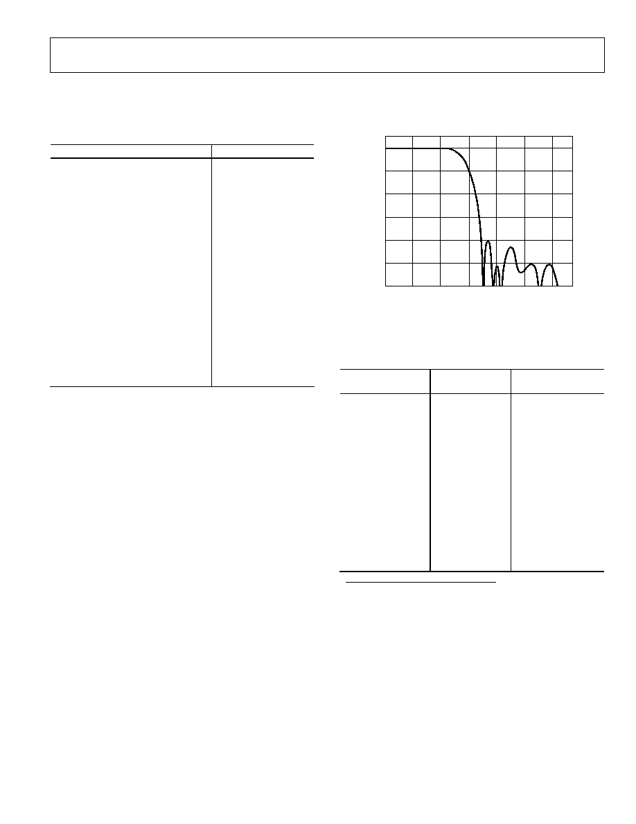
Preliminary Technical Data
ADV7322
Rev. PrA | Page 49 of 88
FILTERS
Table 27 shows an overview of the programmable filters
available on the ADV7322.
Table 27. Selectable Filters
Filter
Subaddress
SD Luma LPF NTSC
0x40
SD Luma LPF PAL
0x40
SD Luma Notch NTSC
0x40
SD Luma Notch PAL
0x40
SD Luma SSAF
0x40
SD Luma CIF
0x40
SD Luma QCIF
0x40
SD Chroma 0.65 MHz
0x40
SD Chroma 1.0 MHz
0x40
SD Chroma 1.3 MHz
0x40
SD Chroma 2.0 MHz
0x40
SD Chroma 3.0 MHz
0x40
SD Chroma CIF
0x40
SD Chroma QCIF
0x40
SD UV SSAF
0x42
HD Chroma Input
0x13
HD Sinc Filter
0x13
HD Chroma SSAF
0x13
SD Internal Filter Response
[Subaddress 0x40 [7:2]; Subaddress 0x42, Bit 0]
The Y filter supports several different frequency responses
including two low-pass responses, two notch responses, an
extended (SSAF) response with or without gain boost
attenuation, a CIF response, and a QCIF response. The UV filter
supports several different frequency responses including six
low-pass responses, a CIF response, and a QCIF response, as
shown in Figure 35 and Figure 36.
If SD SSAF gain is enabled, there is the option of 12 responses
in the range -4 dB to +4 dB [Subaddress 0x47, Bit 4]. The
desired response can be chosen by the user by programming the
correct value via the I
2
C [Subaddress 0x62]. The variation of
frequency responses are shown in Figure 32 and Figure 33.
In addition to the chroma filters listed in Table 27, the
ADV7322 contains an SSAF filter specifically designed for and
applicable to the color difference component outputs, U and V.
This filter has a cutoff frequency of about 2.7 MHz and 40 dB
at 3.8 MHz, as shown in Figure 65. This filter can be controlled
with Address 0x42, Bit 0.
FREQUENCY (MHz)
0
GAIN (
d
B)
10
30
50
60
20
40
6
5
4
3
2
1
0
05067-044
EXTENDED UV FILTER MODE
Figure 65. UV SSAF Filter
If this filter is disabled, the selectable chroma filters shown in
Table 28 can be used for the CVBS or luma/chroma signal.
Table 28. Internal Filter Specifications
Filter
Pass-Band
Ripple
1
(dB)
3 dB Bandwidth
2
(MHz)
Luma LPF NTSC
0.16
4.24
Luma LPF PAL
0.1
4.81
Luma Notch NTSC
0.09
2.3/4.9/6.6
Luma Notch PAL
0.1
3.1/5.6/6.4
Luma SSAF
0.04
6.45
Luma CIF
0.127
3.02
Luma QCIF
Monotonic
1.5
Chroma 0.65 MHz
Monotonic
0.65
Chroma 1.0 MHz
Monotonic
1
Chroma 1.3 MHz
0.09
1.395
Chroma 2.0 MHz
0.048
2.2
Chroma 3.0 MHz
Monotonic
3.2
Chroma CIF
Monotonic
0.65
Chroma QCIF
Monotonic
0.5
1
Pass-band ripple is the maximum fluctuation from the 0 dB response in the
pass band, measured in dB. The pass band is defined to have 0 Hz to fc (Hz)
frequency limits for a low-pass filter, and 0 Hz to f1 (Hz) and f2 (Hz) to infinity
for a notch filter, where fc, f1, and f2 are the -3 dB points.
2
3 dB bandwidth refers to the -3 dB cutoff frequency.
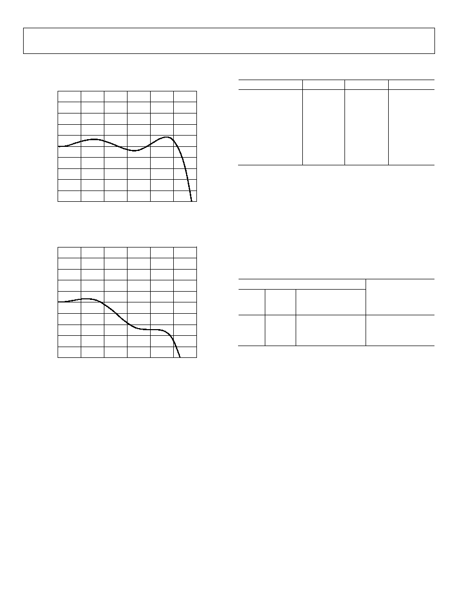
ADV7322
Preliminary Technical Data
Rev. PrA | Page 50 of 88
PS/HD Sinc Filter
[Subaddress 0x13, Bit 3]
FREQUENCY (MHz)
0.5
0.5
30
5
0
GAIN (
d
B)
10
15
20
25
0.4
0.1
0.2
0.3
0.4
0.3
0.2
0
0.1
05067-042
Figure 66. HD Sinc Filter Enabled
FREQUENCY (MHz)
0.5
0.5
30
5
0
GAIN (
d
B)
10
15
20
25
0.4
0.1
0.2
0.3
0.4
0.3
0.2
0
0.1
05067-043
Figure 67. HD Sinc Filter Disabled
COLOR CONTROLS AND RGB MATRIX
HD Y Level, HD Cr Level, HD Cb Level
[Subaddresses 0x16 to 0x18]
Three 8-bit registers at Addresses 0x16, 0x17, and 0x18 are used
to program the output color of the internal HD test pattern
generator, be it the lines of the cross hatch pattern or the
uniform field test pattern. They are not functional as color
controls on external pixel data input. For this purpose the RGB
matrix is used.
The standard used for the values for Y and the color difference
signals to obtain white, black, and the saturated primary and
complementary colors conforms to the ITU-R BT.601-4 standard.
Table 29 shows sample color values to be programmed into the
color registers when Output Standard Selection is set to EIA 770.2.
Table 29. Sample Color Values for EIA 770.2
Output Standard Selection
Sample Color
Y Value
Cr Value
Cb Value
White
235 (EB)
128 (80)
128 (80)
Black
16 (10)
128 (80)
128 (80)
Red
81 (51)
240 (F0)
90 (5A)
Green
145 (91)
34 (22)
54 (36)
Blue
41 (29)
110 (6E)
240 (F0)
Yellow
210 (D2)
146 (92)
16 (10)
Cyan
170 (AA)
16 (10)
166 (A6)
Magenta
106 (6A)
222 (DE)
202 (CA)
RGB Matrix
[Subaddresses 0x03 to 0x09]
The internal RGB matrix automatically takes care of all YCrCb
to RGB scaling according to the input standard programmed in
the device as selected by input mode Register 0x01 [6:4]. Table 30
shows the options available in this Matrix.
Note that it is not possible to do a color space conversion from
RGB-in to YPrPb-out. Also, it is not possible to input SD RGB.
Table 30. Matrix Conversion Options
HDTV/SD/PS
Input Output
Reg 0x02,Bit 5
(YUV/RGB OUT)
Reg 0x15, Bit 1
(RGB IN/YCrCb IN,
PS/HD Only)
YCrCb YPrPb 1
0
YCrCb RGB
0
0
RGB
RGB
0
1
Manual RGB Matrix Adjust Feature
Normally, there is no need to enable this feature in Register
0x02, Bit 3, because the RGB Matrix automatically takes care of
color space conversion depending on the input mode chosen
(SD/PS,HD) and the polarity of RGB/YPrPb output in Register
0x02, Bit 5 (see Table 30). For this reason, manual RGB matrix
adjust feature is turned off by default.
The Manual RGB matrix adjust feature is used in progressive
scan and high definition modes only and is used for custom
coefficient manipulation.
When the manual RGB matrix adjust feature is enabled, the
default values in Registers 0x05 to 0x09 are correct for HDTV
color space only. The color components are converted according
to the 1080i and 720p standards [SMPTE 274M, SMPTE
296M]:
R
= Y + 1.575Pr
G
= Y - 0.468Pr - 0.187Pb
B
= Y + 1.855Pb
Preliminary Technical Data
ADV7322
Rev. PrA | Page 51 of 88
This is reflected in the preprogrammed values for GY = 0x138B,
GU = 0x93, GV = 0x3B, BU = 0x248, and RV = 0x1F0.
Again if RGB matrix is enabled and another input standard is
used (SD or PS), the scale values for GY, GU, GV, BU, and RV
must be adjusted according to this input standard color space.
The user should consider the fact that the color component
conversion might use different scale values. For example,
SMPTE 293M uses the following conversion:
R
= Y + 1.402Pr
G
= Y 0.714Pr 0.344Pb
B
= Y + 1.773Pb
The manual RGB matrix adjust feature can be used to control
the HD output levels in cases where the video output does not
conform to the standard due to altering the DAC output stages
such as termination resistors. The programmable RGB matrix is
used for external HD/PS data and is not functional when
internal test patterns are enabled.
Adjusting Registers 0x05 to 0x09 requires the manual RGB
matrix adjust to be enabled [Register 0x02, Bit 3 =1].
Programming the RGB Matrix
If custom manipulation of coefficients is required, The RGB
matrix is enabled in Address 0x02, Bit 3. The output should be
set to RGB [Address 0x02, Bit 5], sync on PrPb should be
disabled (default) [Address 0x15, Bit 2], and sync on RGB is
optional [Address 0x02, Bit 4].
GY at Addresses 0x03 and 0x05 control the green signal output
levels. BU at Addresses 0x04 and 0x08 control the blue signal
output levels, and RV at Addresses 0x04 and 0x09 control the
red signal output levels. To control YPrPb output levels, YUV
output should be enabled [Address 0x02, Bit 5]. In this case GY
[Address 0x05; Address 0x03, Bits 0 and 1] is used for the Y
output, RV [Address 0x09; Address 0x04, Bits 0 and 1] is used
for the Pr output, and BU [Address 0x08; Address 0x04, Bits 2
and 3] is used for the Pb output.
If RGB output is selected, the RGB matrix scaler uses the
following equations:
G
= GY × Y + GU × Pb + GV × Pr
B
= GY × Y + BU × Pb
R
= GY × Y + RV × Pr
If YPrPb output is selected, the following equations are used:
Y
= GY × Y
U
= BU × Pb
V
= RV × Pr
Upon power-up, the RGB matrix is programmed with the
default values in Table 31.
Table 31. RGB Matrix Default Values
Address Default
0x03 0x03
0x04 0xF0
0x05 0x4E
0x06 0x0E
0x07 0x24
0x08 0x92
0x09 0x7C
When the manual RGB matrix adjust feature is not enabled, the
ADV7322 automatically scales YCrCb inputs to all standards
supported by this part as selected by input mode Register 0x01
[6:4].
SD Luma and Color Control
[Subaddresses 0x5C, 0x5D, 0x 5E, 0x 5F]
SD Y Scale, SD Cr Scale, and SD Cb Scale are three 10-bit-wide
control registers that scale the Y, Cb, and Cr output levels.
Each of these registers represents the value required to scale the
Cb or Cr level from 0.0 to 2.0 and the Y level from 0.0 to 1.5 of
its initial level. The value of these 10 bits is calculated using the
following equation:
Y, Cr, or Cb Scalar Value
= Scale Factor × 512
For example,
Scale Factor
= 1.18
Y, Cb, or Cr Scale Value
= 1.18 × 512 = 665.6
Y, Cb, or Cr Scale Value
= 665 (rounded to the nearest
integer)
Y, Cb, or Cr Scale Value
= 1010 0110 01b
Address 0x5C, SD LSB Register = 0x15
Address 0x5D, SD Y Scale Register = 0xA6
Address 0x5E, SD Cb Scale Register = 0xA6
Address 0x5F, SD Cr Scale Register = 0xA6
Note that this feature affects all interlaced output signals, i.e.,
CVBS, Y-C, YPrPb, and RGB.
SD Hue Adjust Value
[Subaddress 0x60]
The hue adjust value is used to adjust the hue on the composite
and chroma outputs.
These eight bits represent the value required to vary the hue of
the video data, i.e., the variance in phase of the subcarrier
during active video with respect to the phase of the subcarrier
during the color burst. The ADV7322 provides a range of ±22.5°

ADV7322
Preliminary Technical Data
Rev. PrA | Page 52 of 88
increments of 0.17578125°. For normal operation (zero
adjustment), this register is set to 0x80. Values 0xFF and 0x00
represent the upper and lower limits (respectively) of
adjustment attainable.
Hue Adjust (°) = 0.17578125° (HCR
d
- 128) for positive hue
adjust value.
For example, to adjust the hue by +4°, write 0x97 to the Hue
Adjust Value register:
97
x
0
105
128
17578125
.
0
4
=
=
+
d
.
where the sum is rounded to the nearest integer.
To adjust the hue by -4°, write 0x69 to the Hue Adjust Value
register:
69
x
0
105
128
17578125
.
0
4
=
=
+
-
d
where the sum is rounded to the nearest integer.
SD Brightness Control
[Subaddress 0x61]
The brightness is controlled by adding a programmable setup
level onto the scaled Y data. This brightness level may be added
onto the scaled Y data. For NTSC with pedestal, the setup can
vary from 0 IRE to 22.5 IRE. For NTSC without pedestal and
PAL, the setup can vary from -7.5 IRE to +15 IRE.
The brightness control register is an 8-bit register. Seven bits of
this 8-bit register are used to control the brightness level. This
brightness level can be a positive or negative value.
For example,
1. To add +20 IRE brightness level to an NTSC signal with
pedestal , write 0x28 to Address 0x61, SD brightness.
0x[SD Brightness Value] =
0x[IRE Value × 2.015631] =
0x[20 × 2.015631] = 0x[40.31262] = 0x28
2. To add 7 IRE brightness level to a PAL signal, write 0x72 to
Address 0x61, SD brightness.
[IRE Value| × 2.075631
[7 × 2.015631] = [14.109417] = 0001110b
[0001110] into twos complement = [1110010]b = 0x72
Table 32. Brightness Control Values
1
Setup Level In
NTSC with
Pedestal
Setup Level In
NTSC No
Pedestal
Setup
Level In
PAL
SD
Brightness
22.5 IRE
15 IRE
15 IRE
0x1E
15 IRE
7.5 IRE
7.5 IRE
0x0F
7.5 IRE
0 IRE
0 IRE
0x00
0 IRE
7.5 IRE
7.5 IRE
0x71
1
Values in the range from 0x3F to 0x44 might result in an invalid output
signal.
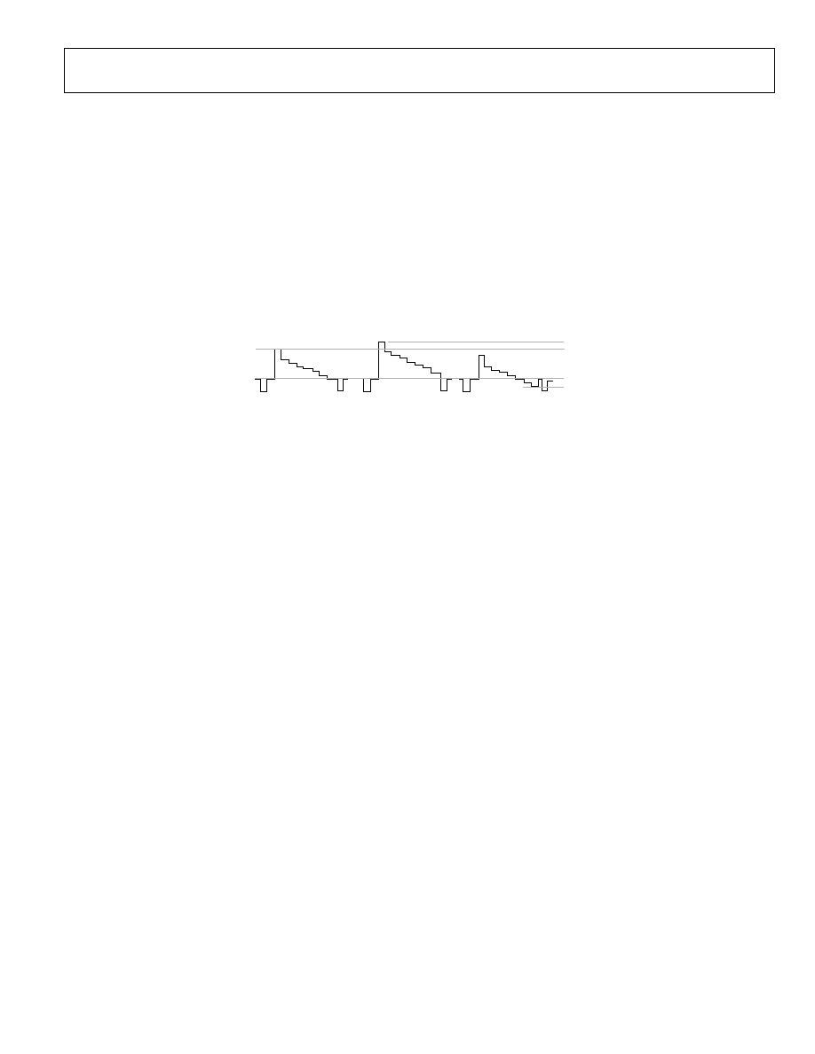
Preliminary Technical Data
ADV7322
Rev. PrA | Page 53 of 88
SD Brightness Detect
[Subaddress 0x7A]
The ADV7322 allows monitoring of the brightness level of the
incoming video data. Brightness detect is a read-only register.
Double Buffering
[Subaddress 0x13, Bit 7; Subaddress 0x48, Bit 2]
Double buffered registers are updated once per field on the
falling edge of the VSYNC signal. Double buffering improves
the overall performance since modifications to register settings
will not be made during active video, but takes effect on the
start of the active video.
Double buffering can be activated on the following HD
registers: HD Gamma A and Gamma B curves and HD CGMS
registers.
Double buffering can be activated on the following SD registers:
SD Gamma A and Gamma B curves, SD Y Scale, SD U Scale, SD
V Scale, SD Brightness, SD Closed Captioning, and SD
Macrovision Bits 5 to 0.
NTSC WITHOUT PEDESTAL
NO SETUP
VALUE ADDED
POSITIVE SETUP
VALUE ADDED
100 IRE
0 IRE
NEGATIVE SETUP
VALUE ADDED
7.5 IRE
+7.5 IRE
05067-069
Figure 68. Examples of Brightness Control Values
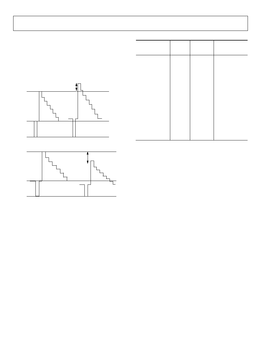
ADV7322
Preliminary Technical Data
Rev. PrA | Page 54 of 88
PROGRAMMABLE DAC GAIN CONTROL
DACs A, B, and C are controlled by REG 0A.
DACs D, E, and F are controlled by REG 0B.
The I
2
C control registers will adjust the output signal gain up or
down from its absolute level.
CASE B
700mV
300mV
NEGATIVE GAIN PROGRAMMED IN
DAC OUTPUT LEVEL REGISTERS,
SUBADDRESS 0x0A, 0x0B
CASE A
GAIN PROGRAMMED IN DAC OUTPUT LEVEL
REGISTERS, SUBADDRESS 0x0A, 0x0B
700mV
300mV
05067-070
Figure 69. Programmable DAC Gain--Positive and Negative Gain
In case A, the video output signal is gained. The absolute level of
the sync tip and blanking level both increase with respect to the
reference video output signal. The overall gain of the signal is
increased from the reference signal.
In case B, the video output signal is reduced. The absolute level
of the sync tip and blanking level both decrease with respect to
the reference video output signal. The overall gain of the signal
is reduced from the reference signal.
The range of this feature is specified for ±7.5% of the nominal
output from the DACs. For example, if the output current of the
DAC is 4.33 mA, the DAC tune feature can change this output
current from 4.008 mA (-7.5%) to 4.658 mA (+7.5%).
The reset value of the vid_out_ctrl registers is 0x00; therefore,
nominal DAC current is output. The following table is an
example of how the output current of the DACs varies for a
nominal 4.33 mA output current.
Table 33. DAC Gain Control
Reg 0x0A or
0x0B
DAC
Current
(mA)
% Gain
Note
0100 0000 (0x40)
4.658
7.5000%
0011 1111 (0x3F)
4.653
7.3820%
0011 1110 (0x3E)
4.648
7.3640%
...
...
...
...
...
...
0000 0010 (0x02)
4.43
0.0360%
0000 0001 (0x01)
4.38
0.0180%
0000 0000 (0x00)
4.33
0.0000%
(I
2
C Reset Value,
Nominal)
1111 1111 (0xFF)
4.25
-0.0180%
1111 1110 (0xFE)
4.23
-0.0360%
...
...
...
...
...
...
1100 0010 (0xC2)
4.018
-7.3640%
1100 0001 (0xC1)
4.013
-7.3820%
1100 0000 (0xC0)
4.008
-7.5000%
GAMMA CORRECTION
[Subaddresses 0x24 to 0x37 for HD,
Subaddresses 0x66 to 0x79 for SD]
Gamma correction is available for SD and HD video. For each
standard, there are twenty 8-bit-wide registers. They are used to
program the gamma correction curves A and B. HD gamma
curve A is programmed at Addresses 0x24 to 0x2D, and HD
gamma curve B is programmed at 0x2E to 0x7. SD gamma
curve A is programmed at Addresses 0x66 to 0x6F, and SD
gamma curve B is programmed at Addresses 0x70 to 0x79.
Generally gamma correction is applied to compensate for the
nonlinear relationship between signal input and brightness level
output (as perceived on the CRT). It can also be applied
wherever nonlinear processing is used.
Gamma correction uses the function
(
)
=
IN
OUT
Signal
Signal
where = gamma power factor.
Gamma correction is performed on the luma data only. The
user may choose either of two curves, curve A or curve B. At
any one time, only one of these curves can be used.
The response of the curve is programmed at 10 predefined
locations. In changing the values at these locations, the gamma
curve can be modified. Between these points, linear
interpolation is used to generate intermediate values.
Considering the curve to have a total length of 256 points, the
10 locations are at 24, 32, 48, 64, 80, 96, 128, 160, 192, and 224.
Locations 0, 16, 240, and 255 are fixed and cannot be changed.
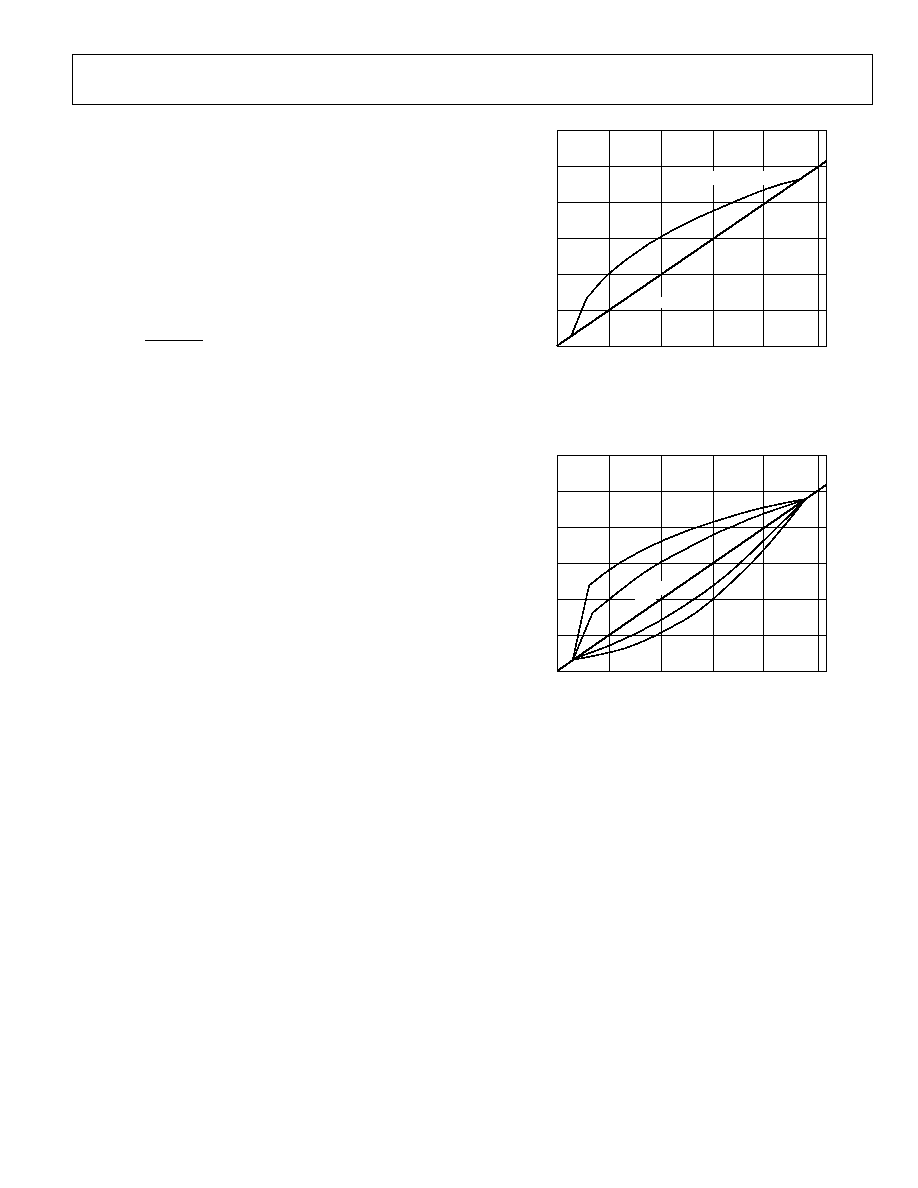
Preliminary Technical Data
ADV7322
Rev. PrA | Page 55 of 88
For the length of 16 to 240, the gamma correction curve has to
be calculated as follows:
y
= x
where:
y
= gamma corrected output
x
= linear input signal
= gamma power factor
To program the gamma correction registers, calculate the seven
values for y using the following formula:
16
)
16
240
(
)
16
240
(
)
16
(
+
-
×
-
=
-
n
n
x
y
where:
x(n - 16) = Value for x along x axis at points
n = 24, 32, 48, 64, 80, 96, 128, 160, 192, or 224
y
n
= Value for y along the y axis, which must be written into the
gamma correction register
For example,
y
24
= [(8/224)0.5 × 224] + 16 = 58
y
32
= [(16/224)0.5 × 224] + 16 = 76
y
48
= [(32/224)0.5 × 224] + 16 = 101
y
64
= [(48/224)0.5 × 224] + 16 =120
y
80
= [(64 / 224)0.5 × 224] + 16 =136
y
96
= [(80 / 224)0.5 × 224] + 16 = 150
y
128
= [(112 / 224)0.5 × 224] + 16 = 174
y
160
= [(144 / 224)0.5 × 224] + 16 = 195
y
192
= [(176 / 224)0.5 × 224] + 16 = 214
y
224
= [(208 / 224)0.5 × 224] + 16 = 232
where the sum of each equation is rounded to the nearest
integer.
The gamma curves in Figure 70 and Figure 71 are examples only;
any user-defined curve is acceptable in the range of 16 to 240.
LOCATION
0
0
50
100
150
200
250
300
50
100
150
200
250
0.5
SIGNAL INPUT
GAMMA CORRE
CTE
D
AMP
L
ITUDE
SIGNAL OUTPUT
GAMMA CORRECTION BLOCK OUTPUT TO A RAMP INPUT
05067-071
Figure 70. Signal Input (Ramp) and Signal Output for Gamma 0.5
LOCATION
0
0
50
100
150
200
250
300
50
100
150
200
250
GAMMA CORRE
CTE
D
AMP
L
ITUDE
GAMMA CORRECTION BLOCK TO A RAMP INPUT FOR
VARIOUS GAMMA VALUES
0.3
0.5
1.5
1.8
SIG
NA
L I
NP
UT
05067-072
Figure 71. Signal Input (Ramp) and Selectable Output Curves
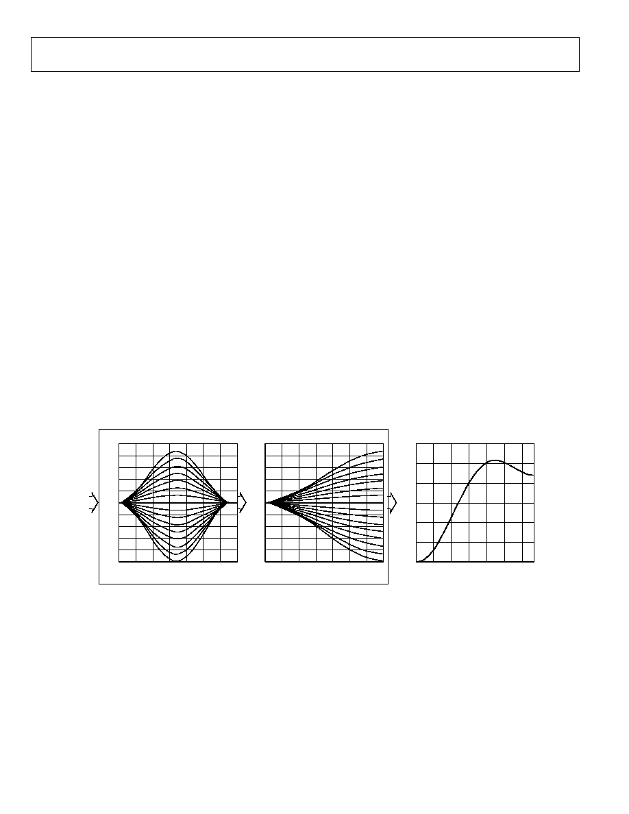
ADV7322
Preliminary Technical Data
Rev. PrA | Page 56 of 88
HD SHARPNESS FILTER AND ADAPTIVE FILTER
CONTROLS
[Subaddresses 0x20, 0x38 to 0x3D]
There are three filter modes available on the ADV7322:
sharpness filter mode and two adaptive filter modes.
HD Sharpness Filter Mode
To enhance or attenuate the Y signal in the frequency ranges
shown in Figure 72, the following register settings must be used:
HD sharpness filter must be enabled and HD adaptive filter
enable must be set to disabled.
To select one of the 256 individual responses, the corresponding
gain values, which range from 8 to +7, for each filter must be
programmed into the HD sharpness filter gain register at
Address 0x20.
HD Adaptive Filter Mode
The HD adaptive filter threshold A, B, and C registers, the HD
adaptive filter gain 1, 2, and 3 registers, and the HD sharpness
gain register are used in adaptive filter mode. To activate the
adaptive filter control, the HD sharpness filter and the HD
adaptive filter must be enabled.
The derivative of the incoming signal is compared to the three
programmable threshold values: HD adaptive filter threshold A,
B, and C. The recommended threshold range is from 16 to 235,
although any value in the range of 0 to 255 can be used.
The edges can then be attenuated with the settings in HD
adaptive filter gain 1, 2, and 3 registers and HD sharpness filter
gain register.
According to the settings of the HD adaptive filter mode
control, there are two adaptive filter modes available:
1.
Mode A is used when adaptive filter mode is set to 0.
In this case, Filter B (LPF) will be used in the adaptive
filter block. Also, only the programmed values for
Gain B in the HD sharpness filter gain and HD
adaptive filter gain 1, 2, and 3 are applied when
needed. The Gain A values are fixed and cannot be
changed.
2.
Mode B is used when adaptive filter mode is set to 1.
In this mode, a cascade of Filter A and Filter B is used.
Both settings for Gain A and Gain B in the HD
sharpness filter gain and HD adaptive filter gain 1, 2,
and 3 become active when needed.
FREQUENCY (MHz)
FILTER A RESPONSE (Gain Ka)
MAGNITUDE
0.5
0.6
0.7
0.8
0.9
1.0
1.1
1.2
1.3
1.4
1.5
FREQUENCY (MHz)
FILTER B RESPONSE (Gain Kb)
MAGNITUDE
0.5
0.6
0.7
0.8
0.9
1.0
1.1
1.2
1.3
1.4
1.5
FREQUENCY (MHz)
M
A
GN
ITU
D
E
R
E
SPON
S
E (
L
inear Scale)
1.0
1.1
1.2
1.3
1.4
1.5
1.6
10
12
INPUT
SIGNAL:
STEP
FREQUENCY RESPONSE IN SHARPNESS
FILTER MODE WITH Ka = 3 AND Kb = 7
SHARPNESS AND ADAPTIVE FILTER CONTROL BLOCK
0
2
4
6
8
05067-073
Figure 72. Sharpness and Adaptive Filter Control Block
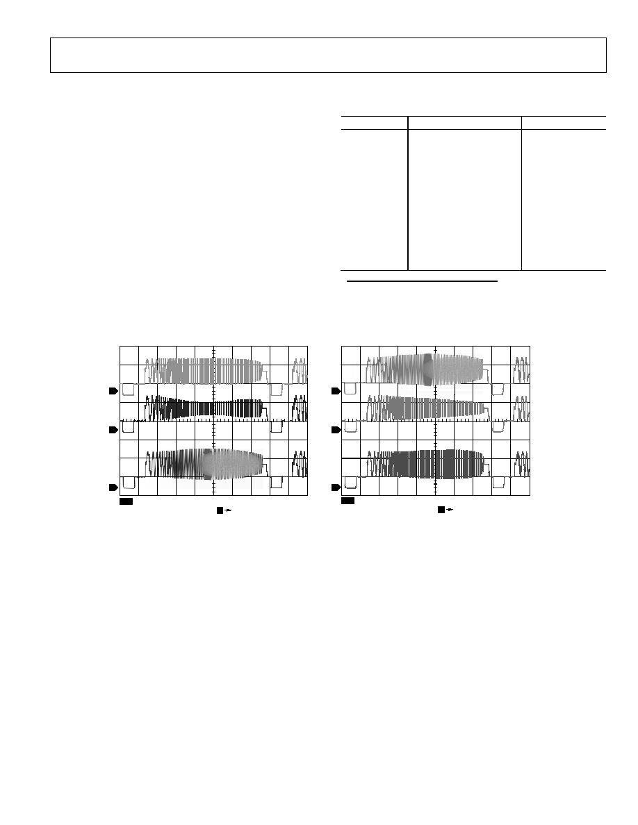
Preliminary Technical Data
ADV7322
Rev. PrA | Page 57 of 88
HD SHARPNESS FILTER AND ADAPTIVE FILTER
APPLICATION EXAMPLES
HD Sharpness Filter Application
The HD sharpness filter can be used to enhance or attenuate the
Y video output signal. The following register settings were used
to achieve the results shown in Figure 73. Input data was
generated by an external signal source.
Table 34. Sharpness Control
Address
Register Setting
Reference
1
0x00 0xFC
0x01 0x10
0x02 0x20
0x10 0x00
0x11 0x81
0x20 0x00
a
0x20 0x08
b
0x20 0x04
c
0x20 0x40
d
0x20 0x80
e
0x20 0x22
f
1
See Figure 73.
f
e
d
a
b
c
1
R4
R2
CH1
500mV
M 4.00
µ
s
CH1
ALL FIELDS
REF A
500mV 4.00
µ
s
1
R2
R1
1
CH1
500mV
M 4.00
µ
s
CH1
ALL FIELDS
REF A
500mV 4.00
µ
s
1
05067-074
9.99978ms
9.99978ms
Figure 73. HD Sharpness Filter Control with Different Gain Settings for HS Sharpness Filter Gain Values
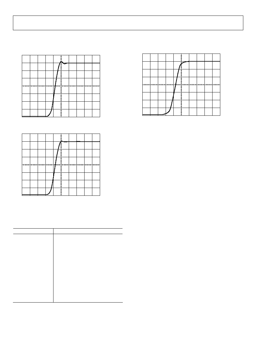
ADV7322
Preliminary Technical Data
Rev. PrA | Page 58 of 88
Adaptive Filter Control Application
Figure 74 and Figure 75 show typical signals to be processed by
the adaptive filter control block.
: 692mV
@: 446mV
: 332ns
@: 12.8ms
05067-075
Figure 74. Input Signal to Adaptive Filter Control
: 692mV
@: 446mV
: 332ns
@: 12.8ms
05067-076
Figure 75. Output Signal after Adaptive Filter Control
The register settings in Table 35 were used to obtain the results
shown in Figure 75, i.e., to remove the ringing on the Y signal.
Input data was generated by an external signal source.
Table 35. Register Settings for Figure 76
Address
Register Setting
0x00 0xFC
0x01 0x38
0x02 0x20
0x10 0x00
0x11 0x81
0x15 0x80
0x20 0x00
0x38 0xAC
0x39 0x9A
0x3A 0x88
0x3B 0x28
0x3C 0x3F
0x3D 0x64
When changing the adaptive filter mode to Mode B
[Address 0x15, Bit 6], the output shown in Figure 76 can be
obtained.
: 674mV
@: 446mV
: 332ns
@: 12.8ms
05067-077
Figure 76. Output Signal from Adaptive Filter Control
SD DIGITAL NOISE REDUCTION
[Subaddresses 0x63, 0x64, 0x65]
DNR is applied to the Y data only. A filter block selects the high
frequency, low amplitude components of the incoming signal
[DNR input select]. The absolute value of the filter output is
compared to a programmable threshold value ['DNR threshold
control]. There are two DNR modes available: DNR mode and
DNR sharpness mode.
In DNR mode, if the absolute value of the filter output is
smaller than the threshold, it is assumed to be noise. A
programmable amount [coring gain border, coring gain data] of
this noise signal will be subtracted from the original signal. In
DNR sharpness mode, if the absolute value of the filter output is
less than the programmed threshold, it is assumed to be noise,
as before. Otherwise, if the level exceeds the threshold, now
being identified as a valid signal, a fraction of the signal [coring
gain border, coring gain data] will be added to the original
signal to boost high frequency components and sharpen the
video image.
In MPEG systems, it is common to process the video
information in blocks of 8 pixels × 8 pixels for MPEG2 systems,
or 16 pixels × 16 pixels for MPEG1 systems [block size control].
DNR can be applied to the resulting block transition areas that
are known to contain noise. Generally, the block transition area
contains two pixels. It is possible to define this area to contain
four pixels [border area].
It is also possible to compensate for variable block positioning
or differences in YCrCb pixel timing with the use of the DNR
block offset
The digital noise reduction registers are three 8-bit registers.
They are used to control the DNR processing.
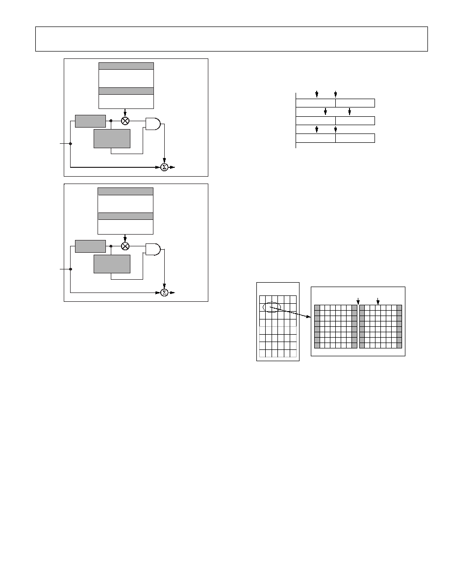
Preliminary Technical Data
ADV7322
Rev. PrA | Page 59 of 88
BLOCK SIZE CONTROL
BORDER AREA
BLOCK OFFSET
CORING GAIN DATA
CORING GAIN BORDER
GAIN
DNR CONTROL
FILTER
OUTPUT
>
THRESHOLD?
INPUT FILTER
BLOCK
FILTER OUTPUT
<
THRESHOLD
DNR OUT
+
+
MAIN SIGNAL PATH
ADD SIGNAL
ABOVE
THRESHOLD
RANGE FROM
ORIGINAL SIGNAL
DNR
SHARPNESS
MODE
NOISE
SIGNAL PATH
Y DATA
INPUT
BLOCK SIZE CONTROL
BORDER AREA
BLOCK OFFSET
CORING GAIN DATA
CORING GAIN BORDER
GAIN
DNR CONTROL
FILTER
OUTPUT
<
THRESHOLD?
INPUT FILTER
BLOCK
FILTER OUTPUT
>
THRESHOLD
DNR OUT
MAIN SIGNAL PATH
SUBTRACT SIGNAL
IN THRESHOLD
RANGE FROM
ORIGINAL SIGNAL
DNR MODE
NOISE
SIGNAL PATH
Y DATA
INPUT
+
05067-078
Figure 77. DNR Block Diagram
CORING GAIN BORDER
[Address 0x63, Bits 3 to 0]
These four bits are assigned to the gain factor applied to border
areas. In DNR mode, the range of gain values is 0 to 1 in
increments of 1/8. This factor is applied to the DNR filter
output, which lies below the set threshold range. The result is
then subtracted from the original signal.
In DNR sharpness mode, the range of gain values is 0 to 0.5 in
increments of 1/16. This factor is applied to the DNR filter
output, which lies above the threshold range. The result is added
to the original signal.
CORING GAIN DATA
[Address 0x63, Bits 7 to 4]
These four bits are assigned to the gain factor applied to the luma
data inside the MPEG pixel block. In DNR mode, the range of
gain values is 0 to 1 in increments of 1/8. This factor is applied
to the DNR filter output, which lies below the set threshold
range. The result is then subtracted from the original signal.
In DNR sharpness mode, the range of gain values is 0 to 0.5 in
increments of 1/16. This factor is applied to the DNR filter
output, which lies above the threshold range. The result is added
to the original signal.
O X X X X X X O O X X X X X X O
O X X X X X X O O X X X X X X O
O X X X X X X O O X X X X X X O
DNR27 DNR24 = 0x01
OFFSET CAUSED
BY VARIATIONS IN
INPUT TIMING
APPLY BORDER
CORING GAIN
APPLY DATA
CORING GAIN
05067-079
Figure 78. DNR Offset Control
DNR THRESHOLD
[Address 0x64, Bits 5 to 0]
These six bits are used to define the threshold value in the range
of 0 to 63. The range is an absolute value.
BORDER AREA
[Address 0x64, Bit 6]
When this bit is set to Logic 1, the block transition area can be
defined to consist of four pixels. If this bit is set to Logic 0, the
border transition area consists of two pixels, where one pixel
refers to two clock cycles at 27 MHz.
720
×
485 PIXELS
(NTSC)
8
×
8 PIXEL BLOCK
2-PIXEL
BORDER DATA
8
×
8 PIXEL BLOCK
05067-080
Figure 79. DNR Border Area
BLOCK SIZE CONTROL
[Address 0x64, Bit 7]
This bit is used to select the size of the data blocks to be
processed. Setting the block size control function to Logic 1
defines a 16 pixel × 16 pixel data block, and Logic 0 defines an
8 pixel × 8 pixel data block, where one pixel refers to two clock
cycles at 27 MHz.
DNR INPUT SELECT CONTROL
[Address 0x65, Bits 2 to 0]
Three bits are assigned to select the filter, which is applied to the
incoming Y data. The signal that lies in the pass band of the
selected filter is the signal that will be DNR processed. Figure 80
shows the filter responses selectable with this control.
ADV7322
Preliminary Technical Data
Rev. PrA | Page 60 of 88
FILTER C
FILTER B
FILTER A
FILTER D
FREQUENCY (Hz)
0
0.2
0.4
0.6
MAGNITUDE
0.8
1.0
05067-081
0
1
2
3
4
5
6
Figure 80. DNR Input Select
DNR MODE CONTROL
[Address 0x65, Bit 4]
This bit controls the DNR mode selected. Logic 0 selects DNR
mode; Logic 1 selects DNR sharpness mode.
DNR works on the principle of defining low amplitude, high
frequency signals as probable noise and subtracting this noise
from the original signal.
In DNR mode, it is possible to subtract a fraction of the signal
that lies below the set threshold, assumed to be noise, from the
original signal. The threshold is set in DNR Register 1.
When DNR sharpness mode is enabled, it is possible to add a
fraction of the signal that lies above the set threshold to the
original signal, since this data is assumed to be valid data and
not noise. The overall effect is that the signal will be boosted
(similar to using Extended SSAF filter).
BLOCK OFFSET CONTROL
[Address 0x65, Bits 7 to 4]
Four bits are assigned to this control, which allows a shift of the
data block of 15 pixels maximum. Consider the coring gain
positions fixed. The block offset shifts the data in steps of one
pixel such that the border coring gain factors can be applied at the
same position regardless of variations in input timing of the data.
SD ACTIVE VIDEO EDGE
[Subaddress 0x42, Bit 7]
When the active video edge feature is enabled, the first three
pixels and the last three pixels of the active video on the luma
channel are scaled so that maximum transitions on these pixels
are not possible. The scaling factors are ×1/8, ×1/2, and ×7/8.
All other active video passes through unprocessed.
SAV/EAV STEP EDGE CONTROL
The ADV7322 has the capability of controlling fast rising and
falling signals at the start and end of active video to minimize
ringing.
An algorithm monitors SAV and EAV and determines when the
edges are rising or falling too fast. The result is reduced ringing
at the start and end of active video for fast transitions.
Subaddress 0x42, Bit 7 = 1, enables this feature.
100 IRE
0 IRE
100 IRE
12.5 IRE
87.5 IRE
0 IRE
50 IRE
LUMA CHANNEL WITH
ACTIVE VIDEO EDGE
DISABLED
LUMA CHANNEL WITH
ACTIVE VIDEO EDGE
ENABLED
05067-082
Figure 81. Example of Active Video Edge Functionality
Preliminary Technical Data
ADV7322
Rev. PrA | Page 61 of 88
VOLTS
0
2
4
F2
L135
6
8
10
12
IRE:FLT
50
0
0
50
100
0.5
05067-083
Figure 82. Address 0x42, Bit 7 = 0
VOLTS
0
2
2
4
6
8
10
12
F2
L135
IRE:FLT
50
0
50
100
0
0.5
05067-084
Figure 83. Address 0x42, Bit 7 = 1
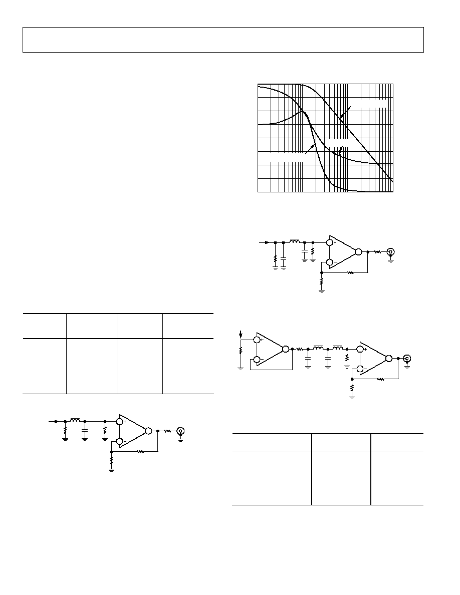
ADV7322
Preliminary Technical Data
Rev. PrA | Page 62 of 88
BOARD DESIGN AND LAYOUT
DAC TERMINATION AND LAYOUT
CONSIDERATIONS
The ADV7322 contains an on-board voltage reference. The
ADV7322 can be used with an external V
REF
(AD1580).
The R
SET
resistors are connected between the R
SET
pins and
AGND and are used to control the full-scale output current and,
therefore, the DAC voltage output levels. For full-scale output,
R
SET
must have a value of 3040 . The RSET values should not
be changed. R
LOAD
has a value of 300 for full-scale output.
VIDEO OUTPUT BUFFER AND OPTIONAL
OUTPUT FILTER
Output buffering on all six DACs is necessary to drive output
devices, such as SD or HD monitors. Analog Devices produces a
range of suitable op amps for this application, for example the
AD8061. More information on line driver buffering circuits is
given in the relevant op amps' data sheets.
An optional analog reconstruction low-pass filter (LPF) may be
required as an anti-imaging filter if the ADV7322 is connected
to a device that requires this filtering.
The filter specifications vary with the application.
Table 36. External Filter Requirements
Application Oversampling
Cutoff
Frequency
(MHz)
Attenuation
50 dB @
(MHz)
SD
2×
>6.5
20.5
SD
16×
>6.5
209.5
PS
1×
>12.5
14.5
PS
8×
>12.5
203.5
HDTV
1×
>30
44.25
HDTV
2×
>30
118.5
560
600
3
4
1
22pF
600
DAC
OUTPUT
75
BNC
OUTPUT
10
µ
H
560
05067-085
Figure 84. Example of Output Filter for SD, 16× Oversampling
0
80
70
60
50
40
30
20
10
0
30
60
90
120
150
180
210
240
1M
10M
100M
FREQUENCY (Hz)
CIRCUIT FREQUENCY RESPONSE
1G
GROUP DELAY (sec)
PHASE (Deg)
MAGNITUDE (dB)
21n
18n
15n
12n
9n
6n
3n
0
24n
GAIN (
d
B)
05067-086
Figure 85. Filter Plot for Output Filter for SD, 16× Oversampling
560
3
4
1
6.8pF
600
6.8pF
600
DAC
OUTPUT
75
BNC
OUTPUT
4.7
µ
H
560
05067-087
Figure 86. Example of Output Filter for PS, 8× Oversampling
82pF
33pF
75
DAC
OUTPUT
220nH
470nH
500
3
4
1
BNC
OUTPUT
500
300
3
4
1
75
05067-088
Figure 87. Example of Output Filter for HDTV, 2× Oversampling
Table 37. Possible Output Rates from the ADV7322
Input Mode Address
0x01, Bits 6 to 4
PLL Address
0x00, Bit 1
Output Rate
(MHz)
Off
27 (2×)
SD Only
On
216 (16×)
Off
27 (1×)
PS Only
On
216 (8×)
HDTV Only
Off On
74.25 (1×)
148.5 (2×)
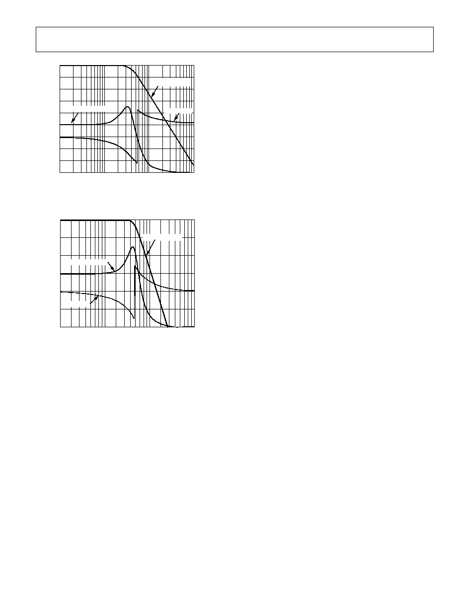
Preliminary Technical Data
ADV7322
Rev. PrA | Page 63 of 88
0
10
20
30
40
50
60
70
80
90
1M
10M
100M
1G
FREQUENCY (Hz)
CIRCUIT FREQUENCY RESPONSE
MAGNITUDE (dB)
GROUP DELAY (Sec)
PHASE (Deg)
GAIN (
d
B)
320
240
160
80
0
80
160
240
480
400
14n
12n
10n
8n
6n
4n
2n
0
18n
16n
05067-089
Figure 88. Filter Plot for Output Filter for PS, 8× Oversampling
0
10
20
30
40
50
60
480
360
240
120
0
120
240
18n
15n
12n
9n
6n
3n
0
1M
10M
100M
1G
FREQUENCY (Hz)
CIRCUIT FREQUENCY RESPONSE
GROUP DELAY (sec)
PHASE (Deg)
MAGNITUDE (dB)
GAIN (
d
B)
05067-090
Figure 89. Filter Plot for Output Filter for HDTV, 2× Oversampling
PCB BOARD LAYOUT
The ADV7322 is optimally designed for lowest noise
performance, both radiated and conducted noise. To
complement the excellent noise performance of the ADV7322,
it is imperative that great care be given to the PC board layout.
The layout should be optimized for lowest noise on the
ADV7322 power and ground lines. This can be achieved by
shielding the digital inputs and providing good decoupling. The
lead length between groups of V
AA
and AGND, V
DD
and DGND,
and V
DD_IO
and GND_IO pins should be kept as short as
possible to minimized inductive ringing.
It is recommended that a 4-layer printed circuit board is used,
with power and ground planes separating the layer of the signal
carrying traces of the components and solder side layer.
Component placement should be carefully considered in order
to separate noisy circuits, such as crystal clocks, high speed logic
circuitry, and analog circuitry.
There should be a separate analog ground plane and a separate
digital ground plane.
Power planes should encompass a digital power plane and an
analog power plane. The analog power plane should contain the
DACs and all associated circuitry, V
REF
circuitry. The digital
power plane should contain all logic circuitry.
The analog and digital power planes should be individually
connected to the common power plane at a single point
through a suitable filtering device, such as a ferrite bead.
DAC output traces on a PCB should be treated as transmission
lines. It is recommended that the DACs be placed as close as
possible to the output connector, with the analog output traces
being as short as possible (less than 3 inches). The DAC
termination resistors should be placed as close as possible to the
DAC outputs and should overlay the PCB's ground plane. As
well as minimizing reflections, short analog output traces will
reduce noise pickup due to neighboring digital circuitry.
To avoid crosstalk between the DAC outputs, it is recommended
that as much space as possible be left between the tracks of the
individual DAC output pins. The addition of ground tracks
between outputs is also recommended.
Supply Decoupling
Noise on the analog power plane can be further reduced by the
use of decoupling capacitors.
Optimum performance is achieved by the use of 10 nF and
0.1 µF ceramic capacitors. Each group of V
AA
, V
DD
, or V
DD_IO
pins should be individually decoupled to ground. This should
be done by placing the capacitors as close as possible to the
device with the capacitor leads as short as possible, thus
minimizing lead inductance.
A 1 µF tantalum capacitor is recommended across the V
AA
supply in addition to 10 nF ceramic. See the circuit layout in
Figure 90.
Digital Signal Interconnect
The digital signal lines should be isolated as much as possible
from the analog outputs and other analog circuitry. Digital
signal lines should not overlay the analog power plane.
Due to the high clock rates used, avoid long clock lines to the
ADV7322 to minimize noise pickup.
Any active pull-up termination resistors for the digital inputs
should be connected to the digital power plane and not the
analog power plane.
Analog Signal Interconnect
Locate the ADV7322 as close as possible to the output
connectors to minimize noise pickup and reflections due to
impedance mismatch.
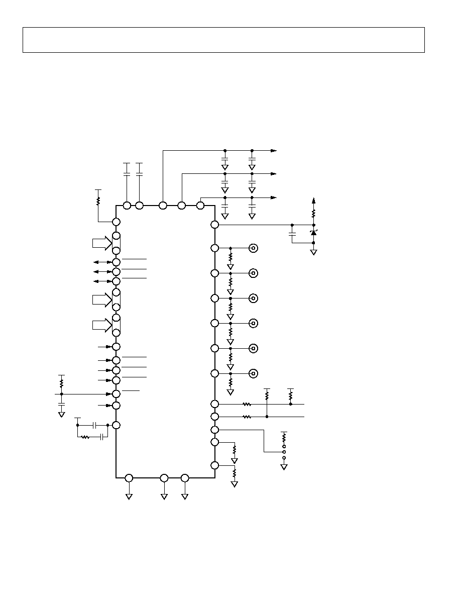
ADV7322
Preliminary Technical Data
Rev. PrA | Page 64 of 88
For optimum performance, the analog outputs should each be
source and load terminated, as shown in Figure 90. The
termination resistors should be as close as possible to the
ADV7322 to minimize reflections.
For optimum performance, it is recommended that all
decoupling and external components relating to the ADV7322
be located on the same side of the PCB and as close as possible
to the ADV7322. Any unused inputs should be tied to ground.
5k
V
DD_IO
5k
V
DD_IO
COMP1, 2
45
V
AA
41
V
DD
V
DD_IO
1
ADV7322
I
2
C
19
50
49
48
23
CLKIN_B
63
24
25
33
CLKIN_A
32
EXT_LF
34
UNUSED
INPUTS
SHOULD BE
GROUNDED
C0C7
S0S7
Y0Y7
V
AA
4.7
µ
F
+
4.7k
820pF
3.9nF
V
AA
GND_ IO
64
AGND
40
DGND
11, 57
I
2
C BUS
10nF
0.1
µ
F
10nF
0.1
µ
F
10, 56
V
DD_IO
V
DD
10nF
1
µ
F
V
AA
+
V
AA
0.1
µ
F
POWER SUPPLY DECOUPLING
FOR EACH POWER SUPPLY GROUP
36
V
AA
0.1
µ
F
DAC D
39
300
DAC E
38
300
DAC F
37
300
DAC A
44
300
DAC B
43
300
DAC C
42
300
V
REF 46
100nF
1.1k
V
AA
RECOMMENDED EXTERNAL
AD1580 FOR OPTIMUM
PERFORMANCE
5k
V
DD_IO
SCLK
22
100
680
SDA
21
ALSB
20
R
SET1
R
SET2
47
100
3040
SELECTION HERE
DETERMINES
DEVICE ADDRESS
35
3040
5k
V
DD_IO
S_HSYNC
S_VSYNC
S_BLANK
P_HSYNC
P_VSYNC
P_BLANK
RESET
05067-
091
Figure 90. ADV7322 Circuit Layout

Preliminary Technical Data
ADV7322
Rev. PrA | Page 65 of 88
APPENDIX 1--COPY GENERATION MANAGEMENT SYSTEM
PS CGMS
Data Registers 2 to 0
[Subaddresses 0x21, 0x22, 0x23]
525p
Using the vertical blanking interval 525p system, 525p CGMS
conforms to the CGMS-A EIA-J CPR1204-1 (March 1998)
transfer method of video identification information and to the
IEC61880 (1998) 525p/60 video system's analog interface for the
video and accompanying data.
When PS CGMS is enabled [Subaddress 0x12, Bit 6 = 1], CGMS
data is inserted on Line 41. The 525p CGMS data registers are at
Addresses 0x21, 0x22, and 0x23.
625p
The 625p CGMS conforms to the IEC62375 (2004) 625p/50
video system's analog interface for the video and accompanying
data using the vertical blanking interval.
When PS CGMS is enabled [Subaddress 0x12, Bit 6 = 1], CGMS
data is inserted on Line 43. The 625p CGMS data registers are at
Addresses 0x22, and 0x23.
HD CGMS
[Address 0x12, Bit 6]
The ADV7322 supports Copy Generation Management System
(CGMS) in HDTV mode (720p and 1080i) in accordance with
EIAJ CPR-1204-2.
The HD CGMS data registers are found at Addresses 0x021,
0x22, and 0x23.
SD CGMS
Data Registers 2 to 0
[Subaddresses 0x59, 0x5A, 0x5B]
The ADV7322 supports Copy Generation Management System
(CGMS), conforming to the standard. CGMS data is
transmitted on Line 20 of the odd fields and Line 283 of even
fields. Bits C/W05 and C/W06 control whether CGMS data is
output on odd and even fields. CGMS data can be transmitted
only when the ADV7322 is configured in NTSC mode. The
CGMS data is 20 bits long, and the function of each of these bits
is as shown in the following table. The CGMS data is preceded
by a reference pulse of the same amplitude and duration as a
CGMS bit; see Figure 93.
FUNCTION OF CGMS BITS
For Word 0 to 6 bits, Word 1 to 4 bits, and Word 2 to 6 bits CRC
6 bits,
1
6
+
+
=
x
x
Polynomial
CRC
where default is preset to 111111.
720p System
CGMS data is applied to Line 24 of the luminance vertical
blanking interval.
1080i System
CGMS data is applied to Line 19 and Line 582 of the luminance
vertical blanking interval.
CGMS FUNCTIONALITY
If SD CGMS CRC [Address 0x59, Bit 4] or PS/HD CGMS CRC
[Subaddress 0x12, Bit 7] is set to Logic 1, the last six bits, C19 to
C14, which comprise the 6-bit CRC check sequence, are
calculated automatically on the ADV7322 based on the lower
14 bits (C0 to C13) of the data in the data registers and output
with the remaining 14 bits to form the complete 20 bits of the
CGMS data. The calculation of the CRC sequence is based on
the polynomial ×6 + x + 1 with a preset value of 111111. If SD
CGMS CRC [Address 0x59, Bit 4] and PS/HD CGMS CRC
[Address 0x12, Bit 7] are set to Logic 0, all 20 bits (C0 to C19)
are output directly from the CGMS registers (no CRC is
calculated, must be calculated by the user).
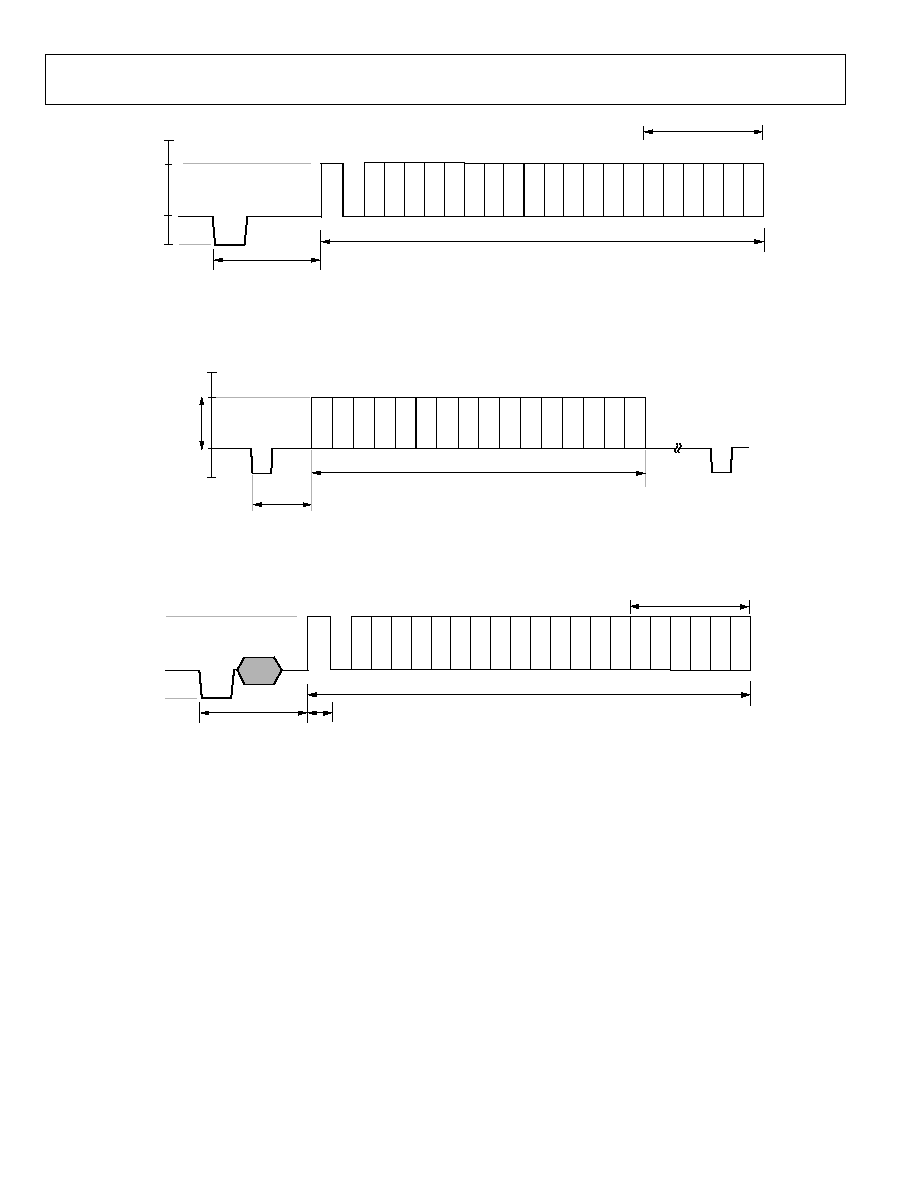
ADV7322
Preliminary Technical Data
Rev. PrA | Page 66 of 88
C0 C1 C2 C3 C4 C5 C6 C7 C8 C9 C10 C11 C12
CRC SEQUENCE
REF
5.8
µ
s
±
0.15
µ
s
6T
0mV
300mV
70%
±
10%
T = 1/(
f
H
×
33) = 963ns
f
H
= HORIZONTAL SCAN FREQUENCY
T
±
30ns
+700mV
BIT1 BIT2. . . . . . . . . . . . . . . . . . . . . . . . . . . . . . . . . . . . . . . . . . . . . . . . . . . . . . . . . . . . . . . . . . . .BIT20
21.2
µ
s
±
0.22
µ
s
22T
05067-092
C13 C14 C15 C16 C17 C18 C19
Figure 91. Progressive Scan 525p CGMS Waveform (Line 41)
R
S
C0
LSB C1 C2 C3 C4 C5 C6 C7 C8 C9 C10 C11 C12
C13
MSB
PEAK WHITE
SYNC LEVEL
500mV
±
25mV
5.5
µ
s
±
0.125
µ
s
R = RUN-IN
S = START CODE
13.7
µ
s
05067-093
Figure 92. Progressive Scan 625p CGMS-A Waveform (Line 43)
CRC SEQUENCE
REF
0 IRE
40 IRE
+70 IRE
+100 IRE
05067-094
11.2
µ
s
2.235
µ
s
±
20ns
49.1
µ
s
±
0.5
µ
s
C0 C1 C2 C3 C4 C5 C6 C7 C8 C9 C10 C11 C12 C13 C14 C15 C16 C17 C18 C19
Figure 93. Standard Definition CGMS Waveform
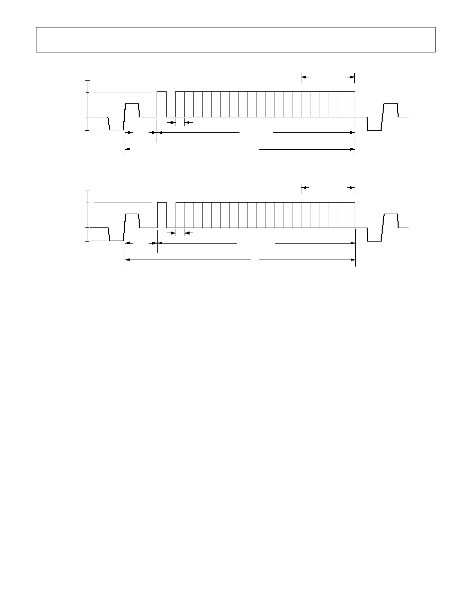
Preliminary Technical Data
ADV7322
Rev. PrA | Page 67 of 88
CRC SEQUENCE
REF
4T
3.128
µ
s
±
90ns
17.2
µ
s
±
160ns
22T
T = 1/(
f
H
×
1650/58) = 781.93ns
f
H
= HORIZONTAL SCAN FREQUENCY
1H
T
±
30ns
0mV
300mV
70%
±
10%
+700mV
BIT1 BIT2. . . . . . . . . . . . . . . . . . . . . . . . . . . . . . . . . . . . . . . . . . . . . . . . . . . . . . . . . . . BIT20
C0
C1
C2
C3
C4
C5
C6
C7
C8
C9 C10 C11 C12 C13 C14 C15 C16 C17 C18 C19
05067-095
Figure 94. HDTV 720p CGMS Waveform
CRC SEQUENCE
REF
4T
4.15
µ
s
±
60ns
22.84
µ
s
±
210ns
22T
T = 1/(f
H
×
2200/77) = 1.038
µ
s
f
H
= HORIZONTAL SCAN FREQUENCY
1H
T
±
30ns
0mV
300mV
70%
±
10%
+700mV
BIT1 BIT2. . . . . . . . . . . . . . . . . . . . . . . . . . . . . . . . . . . . . . . . . . . . . . . . . . . . . . . . . . . BIT20
C0
C1
C2
C3
C4
C5
C6
C7
C8
C9 C10 C11 C12 C13 C14 C15 C16 C17 C18 C19
05067-096
Figure 95. HDTV 1080i CGMS Waveform
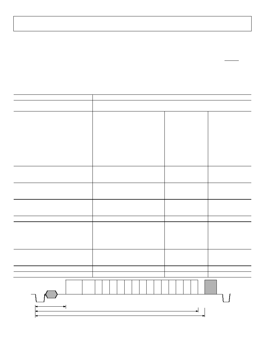
ADV7322
Preliminary Technical Data
Rev. PrA | Page 68 of 88
APPENDIX 2--SD WIDE SCREEN SIGNALING
[Subaddresses 0x59, 0x5A, 0x5B]
The ADV7322 supports wide screen signaling (WSS)
conforming to the standard. WSS data is transmitted on Line 23.
WSS data can be transmitted only when the device is
configured in PAL mode. The WSS data is 14 bits long, and the
function of each of these bits is shown in Table 38. The WSS
data is preceded by a run-in sequence and a start code; see
Figure 95. If SD WSS [Address 0x59, Bit 7] is set to Logic 1, it
enables the WSS data to be transmitted on Line 23. The latter
portion of Line 23 (42.5 s from the falling edge of HSYNC) is
available for the insertion of video. It is possible to blank the
WSS portion of Line 23 with Subaddress 0x61, Bit 7.
Table 38. Function of WSS Bits
Bit
Description
Bit 0 to Bit 2
Aspect Ratio/Format/Position
Bit 3
Odd Parity Check of Bit 0 to Bit 2
B0
B1
B2
B3
Aspect Ratio
Format
Position
0
0 0 1
4:3
Full
Format
N/A
1
0 0 0
14:9
Letterbox
Center
0
1 0 0
14:9
Letterbox
Top
1
1 0 1
16:9
Letterbox
Center
0
0 1 0
16:9
Letterbox
Top
1
0 1 1
>16:9
Letterbox
Center
0
1 1 1
14:9
Full
Format
Center
1
1 1 0
16:9
N/A
N/A
1
1 1 0
16:9
B4
0
Camera Mode
1
Film Mode
B5
0
Standard Coding
1
Motion Adaptive Color Plus
B6
0
No Helper
1
Modulated Helper
B7
Reserved
B9
B10
0
0
No Open Subtitles
1
0
Subtitles in Active Image Area
0
1
Subtitles out of Active Image Area
1
1
Reserved
B11
0
No Surround Sound Information
1
Surround Sound Mode
B12
Reserved
B13
Reserved
ACTIVE
VIDEO
RUN-IN
SEQUENCE
START
CODE
500mV
11.0
µ
s
38.4
µ
s
42.5
µ
s
W0
W1
W2
W3
W4
W5
W6
W7
W8
W9 W10 W11 W12 W13
05067-097
Figure 96. WSS Waveform Diagram
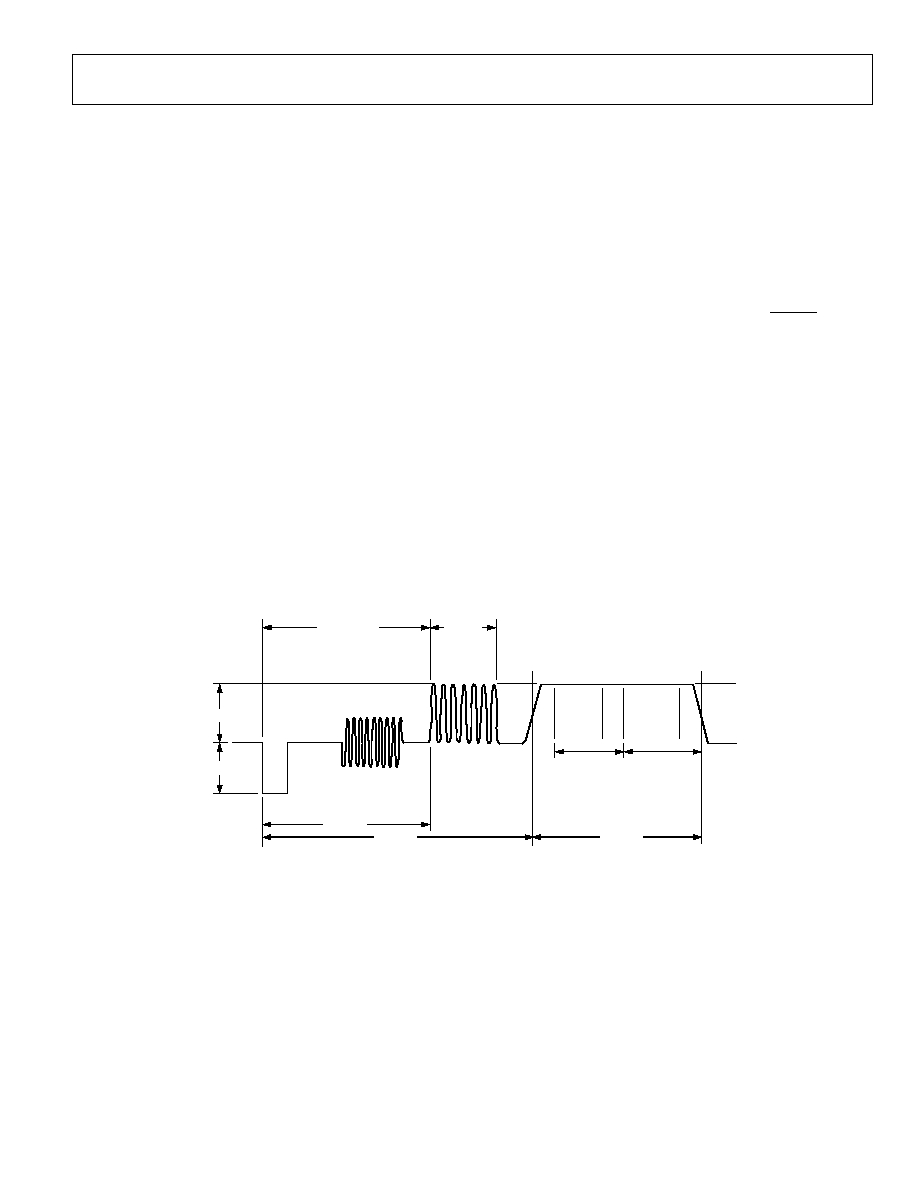
Preliminary Technical Data
ADV7322
Rev. PrA | Page 69 of 88
APPENDIX 3--SD CLOSED CAPTIONING
[Subaddresses 0x51 to 0x54]
The ADV7322 supports closed captioning conforming to the
standard television synchronizing waveform for color
transmission. Closed captioning is transmitted during the
blanked active line time of Line 21 of the odd fields and Line
284 of the even fields.
Closed captioning consists of a 7-cycle sinusoidal burst that is
frequency and phase locked to the caption data. After the clock
run-in signal, the blanking level is held for two data bits and is
followed by Logic 1 start bit. Sixteen bits of data follow the start
bit. These consist of two 8-bit bytes, seven data bits, and one
odd parity bit. The data for these bytes is stored in the SD closed
captioning registers [Addresses 0x53 to 0x54].
The ADV7322 also supports the extended closed captioning
operation, which is active during even fields and encoded on
Scan Line 284. The data for this operation is stored in the SD
closed captioning registers [Addresses 0x51 to 0x52].
All clock run-in signals and timing to support closed captioning
on Lines 21 and 284 are generated automatically by the
ADV7322. All pixels inputs are ignored during Lines 21 and 284
if closed captioning is enabled.
FCC Code of Federal Regulations (CFR) 47 section 15.119 and
EIA608 describe the closed captioning information for Lines 21
and 284.
The ADV7322 uses a single buffering method. This means that
the closed captioning buffer is only 1 byte deep; therefore, there
will be no frame delay in outputting the closed captioning data,
unlike other 2-byte-deep buffering systems. The data must be
loaded one line before it is output on Line 21 and Line 284. A
typical implementation of this method is to use VSYNC to
interrupt a microprocessor, which in turn will load the new data
(two bytes) in every field. If no new data is required for
transmission, 0s must be inserted in both data registers; this is
called nulling. It is also important to load control codes, all of
which are double bytes, on Line 21, or a TV will not recognize
them. If there is a message like "Hello World" that has an odd
number of characters, it is important to pad it out to even to get
"end of caption" 2-byte control code to land in the same field.
D0D6
D0D6
10.5
±
0.25
µ
s
12.91
µ
s
7 CYCLES OF
0.5035MHz
CLOCK RUN-IN
REFERENCE COLOR BURST
(9 CYCLES)
FREQUENCY = F
SC
= 3.579545MHz
AMPLITUDE = 40 IRE
50 IRE
40 IRE
10.003
µ
s
27.382
µ
s
33.764
µ
s
BYTE 1
BYTE 0
TWO 7-BIT + PARITY
ASCII CHARACTERS
(DATA)
S
T
A
R
T
P
A
R
I
T
Y
P
A
R
I
T
Y
05067-098
Figure 97. Closed Captioning Waveform, NTSC
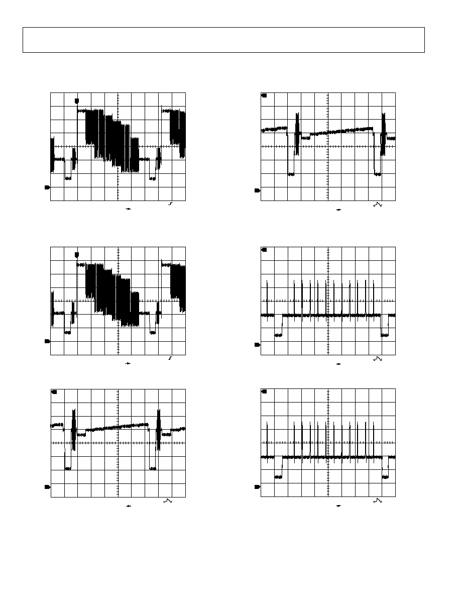
ADV7322
Preliminary Technical Data
Rev. PrA | Page 70 of 88
APPENDIX 4--TEST PATTERNS
The ADV7322 can generate SD and HD test patterns.
CH2 200mV
M 10.0
µ
s
A CH2 1.20V
T
30.6000
µ
s
2
T
05067-099
Figure 98. NTSC Color Bars
CH2 200mV
M 10.0
µ
s
A CH2 1.21V
T
30.6000
µ
s
2
T
05067-100
Figure 99. PAL Color Bars
CH2 100mV
M 10.0
µ
s
CH2 EVEN
T
1.82380ms
2
T
05067-101
Figure 100. NTSC Black Bar [21 mV, 0 mV, 3.5 mV, 7 mV, 10.5 mV, 14 mV,
18 mV, 23 mV]
CH2 100mV
M 10.0
µ
s
CH2 EVEN
T
1.82600ms
2
T
05067-102
Figure 101. PAL Black Bar [21 mV, 0 mV, 3.5 mV, 7 mV, 10.5 mV, 14 mV,
18 mV, 23 mV]
CH2 200mV
M 4.0
µ
s
CH2 EVEN
T
1.82944ms
2
T
05067-103
Figure 102. 525p Hatch Pattern
CH2 200mV
M 4.0
µ
s
CH2 EVEN
T
1.84208ms
2
T
05067-104
Figure 103. 625p Hatch Pattern
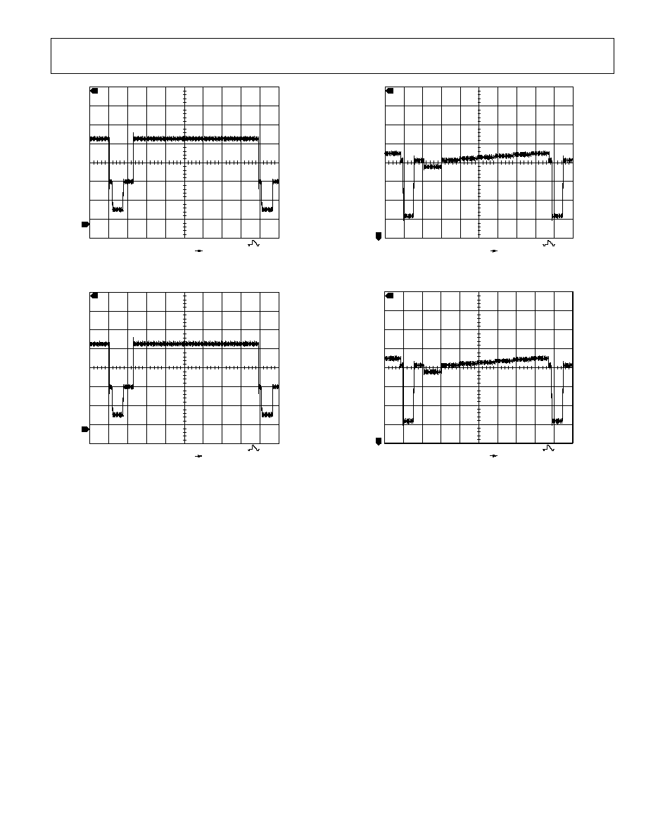
Preliminary Technical Data
ADV7322
Rev. PrA | Page 71 of 88
CH2 200mV
M 4.0
µ
s
CH2 EVEN
T
1.82872ms
2
T
05067-105
Figure 104. 525p Field Pattern
CH2 200mV
M 4.0
µ
s
CH2 EVEN
T
1.84176ms
2
T
05067-106
Figure 105. 625p Field Pattern
CH2 100mV
M 4.0
µ
s
CH2 EVEN
T
1.82936ms
2
T
05067-107
Figure 106. 525p Black Bar [-35 mV, 0 mV, 7 mV, 14 mV, 21 mV,
28 mV, 35 mV]
CH2 100mV
M 4.0
µ
s
CH2 EVEN
T
1.84176ms
2
T
05067-108
Figure 107. 625p Black Bar [-35 mV, 0 mV, 7 mV, 14 mV,
21 mV, 28 mV, 5 mV]
ADV7322
Preliminary Technical Data
Rev. PrA | Page 72 of 88
The register settings in Table 39 are used to generate an SD
NTSC CVBS output on DAC A, S-video on DACs B and C, and
YPrPb on DACs D, E, and F. Upon power-up, the subcarrier
registers are programmed with the appropriate values for NTSC.
All other registers are set as normal/default.
Table 39. NTSC Test Pattern Register Writes
Subaddress
Register Setting
0x00 0xFC
0x40 0x10
0x42 0x40
0x44
0x40 (internal test pattern on)
0x4A 0x08
For PAL CVBS output on DAC A, the same settings are used,
except that Subaddress 0x40 is programmed to 0x11 and the Fsc
registers are programmed as shown in Table 40.
Table 40. PAL Fsc Register Writes
Subaddress
Description
Register Setting
0x4C Fsc0
0xCB
0x4D Fsc1
0x8A
0x4E Fsc2
0x09
0x4F Fsc3
0x2A
Note that when programming the Fsc registers, the user must
write the values in the sequence Fsc0, Fsc1, Fsc2, Fsc3. The full
Fsc value to be written is only accepted after the Fsc3 write is
complete.
The register settings in Table 41 are used to generate a 525p
hatch pattern on DAC D, E, and F. All other registers are set as
normal/default.
Table 41. 525p Test Pattern Register Writes.
Subaddress
Register Setting
Ox00 0xFC
0x01 0x10
0x10 0x00
0x11 0x05
0x16 0xA0
0x17 0x80
0x18 0x80
For 625p hatch pattern on DAC D, the same register settings are
used except that Subaddress 0x10 = 0x18.
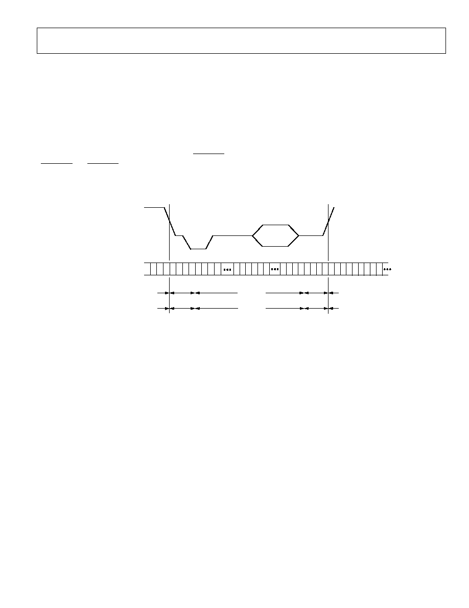
Preliminary Technical Data
ADV7322
Rev. PrA | Page 73 of 88
APPENDIX 5--SD TIMING MODES
[Subaddress 0x4A]
MODE 0 (CCIR-656)--SLAVE OPTION
(TIMING REGISTER 0 TR0 = X X X X X 0 0 0)
The ADV7322 is controlled by the SAV (start active video) and
EAV (end active video) time codes in the pixel data. All timing
information is transmitted using a 4-byte synchronization
pattern. A synchronization pattern is sent immediately before
and after each line during active picture and retrace. S_VSYNC,
S_HSYNC, and S_BLANK (if not used) pins should be tied high
during this mode. Blank output is available.
Y Cr Y
F
F
0
0
0
0
X
Y
8
0
1
0
8
0
1
0
F
F
0
0
F
F
A
B
A
B
A
B
8
0
1
0
8
0
1
0
F
F
0
0
0
0
X
Y
C
b
Y C
r
C
b
Y
C
b
Y
C
r
EAV CODE
SAV CODE
ANCILLARY DATA
(HANC)
4 CLOCK
4 CLOCK
268 CLOCK
1440 CLOCK
4 CLOCK
4 CLOCK
280 CLOCK
1440 CLOCK
END OF ACTIVE
VIDEO LINE
START OF ACTIVE
VIDEO LINE
ANALOG
VIDEO
INPUT PIXELS
NTSC/PAL M SYSTEM
(525 LINES/60Hz)
PAL SYSTEM
(625 LINES/50Hz)
Y
05067-109
Figure 108. SD Slave Mode 0
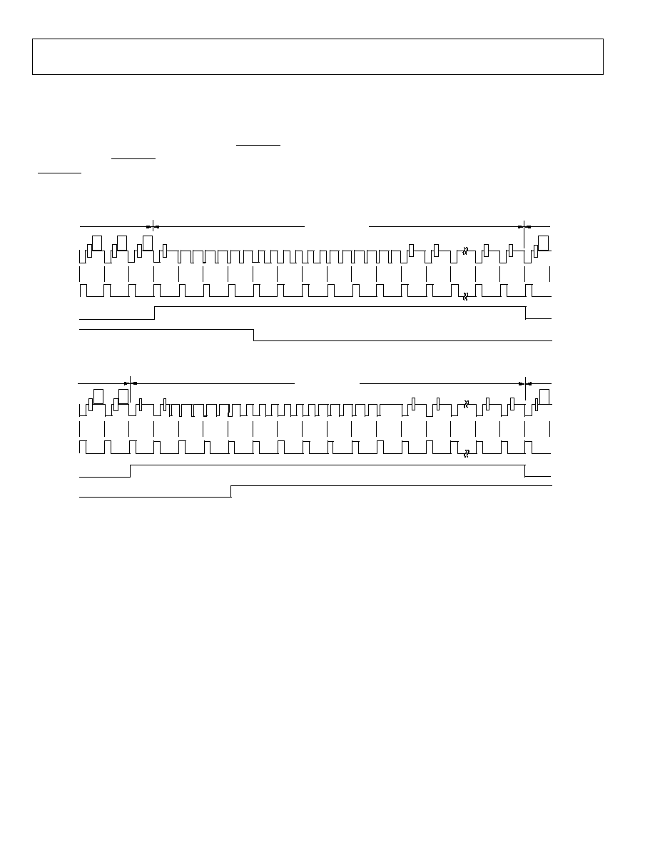
ADV7322
Preliminary Technical Data
Rev. PrA | Page 74 of 88
MODE 0 (CCIR-656)--MASTER OPTION
(TIMING REGISTER 0 TR0 = X X X X X 0 0 1)
The ADV7322 generates H, V, and F signals required for the
SAV (start active video) and EAV (end active video) time codes
in the CCIR656 standard. The H bit is output on S_HSYNC, the
V bit is output on S_BLANK, and the F bit is output on
S_VSYNC.
522
523
524
525
8
9
10
11
20
21
22
DISPLAY
DISPLAY
VERTICAL BLANK
ODD FIELD
EVEN FIELD
H
V
F
260
261
262
263
264
265
266
267
268
269
270
271
272
273
274
283
284
285
ODD FIELD
EVEN FIELD
DISPLAY
DISPLAY
VERTICAL BLANK
H
V
F
05067-110
7
6
5
4
3
2
1
Figure 109. SD Master Mode 0, NTSC
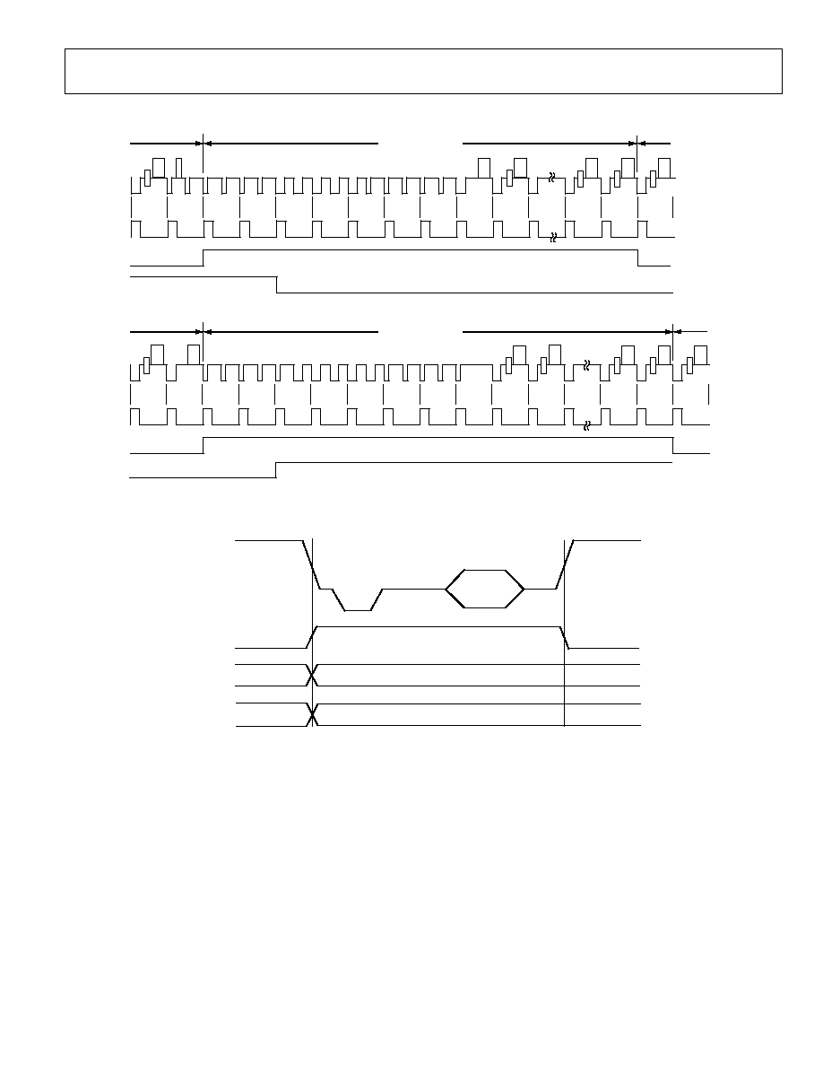
Preliminary Technical Data
ADV7322
Rev. PrA | Page 75 of 88
622
623
624
625
21
22
23
DISPLAY
DISPLAY
VERTICAL BLANK
H
V
F
ODD FIELD
EVEN FIELD
309
310
311
312
314
315
316
317
318
319
320
334
335
336
DISPLAY
DISPLAY
VERTICAL BLANK
H
V
F
ODD FIELD
EVEN FIELD
313
05067-111
7
6
5
4
3
2
1
Figure 110. SD Master Mode 0, PAL
ANALOG
VIDEO
H
F
V
05067-112
Figure 111. SD Master Mode 0, Data Transitions
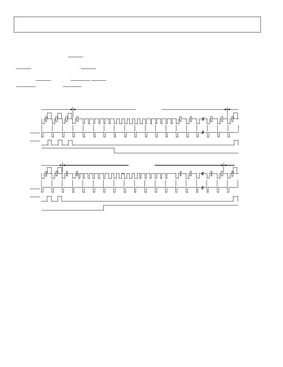
ADV7322
Preliminary Technical Data
Rev. PrA | Page 76 of 88
MODE 1--SLAVE OPTION
(TIMING REGISTER 0 TR0 = X X X X X 0 1 0)
In this mode, the ADV7322 accepts horizontal sync and
odd/even field signals. When HSYNC is low, a transition of the
field input indicates a new frame, i.e., vertical retrace. The
BLANK signal is optional. When the BLANK input is disabled,
ADV7322 automatically blanks all normally blank lines as per
CCIR-624. HSYNC is input on S_HSYNC, BLANK on
S_BLANK, and FIELD on S_VSYNC.
260
261
262
263
264
265
266
267
268
269
270
271
272
273
274
283
284
285
ODD FIELD
EVEN FIELD
DISPLAY
DISPLAY
VERTICAL BLANK
522
523
524
525
5
9
10
11
20
21
22
DISPLAY
DISPLAY
VERTICAL BLANK
ODD FIELD
EVEN FIELD
FIELD
FIELD
HSYNC
BLANK
HSYNC
BLANK
05067-113
7
6
4
3
2
1
8
Figure 112. SD Slave Mode 1 (NTSC)
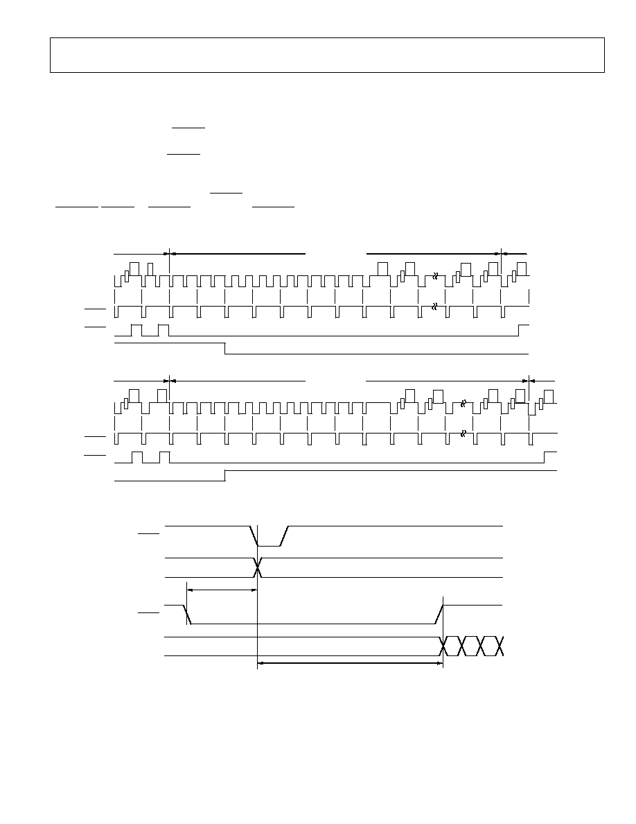
Preliminary Technical Data
ADV7322
Rev. PrA | Page 77 of 88
MODE 1--MASTER OPTION
(TIMING REGISTER 0 TR0 = X X X X X 0 1 1)
In this mode, the ADV7322 can generate horizontal sync and
odd/even field signals. When HSYNC is low, a transition of the
field input indicates a new frame, i.e., vertical retrace. The blank
signal is optional. When the BLANK input is disabled,
ADV7322 automatically blanks all normally blank lines as per
CCIR-624. Pixel data is latched on the rising clock edge
following the timing signal transitions. HSYNC is output on the
S_HSYNC, BLANK on S_BLANK, and FIELD on S_VSYNC.
622
623
624
625
21
22
23
DISPLAY
VERTICAL BLANK
ODD FIELD
EVEN FIELD
FIELD
DISPLAY
309
310
311
312
313
314
315
316
317
318
319
334
335
336
DISPLAY
VERTICAL BLANK
ODD FIELD
EVEN FIELD
DISPLAY
320
FIELD
5
7
6
4
3
2
1
HSYNC
BLANK
HSYNC
BLANK
05067-114
Figure 113. SD Slave Mode 1 (PAL)
FIELD
PIXEL
DATA
PAL = 12
×
CLOCK/2
NTSC = 16
×
CLOCK/2
Cb
Y
Cr
Y
HSYNC
BLANK
PAL = 132
×
CLOCK/2
NTSC = 122
×
CLOCK/2
05067-115
Figure 114. SD Timing Mode 1--Odd/Even Field Transitions Master/Slave
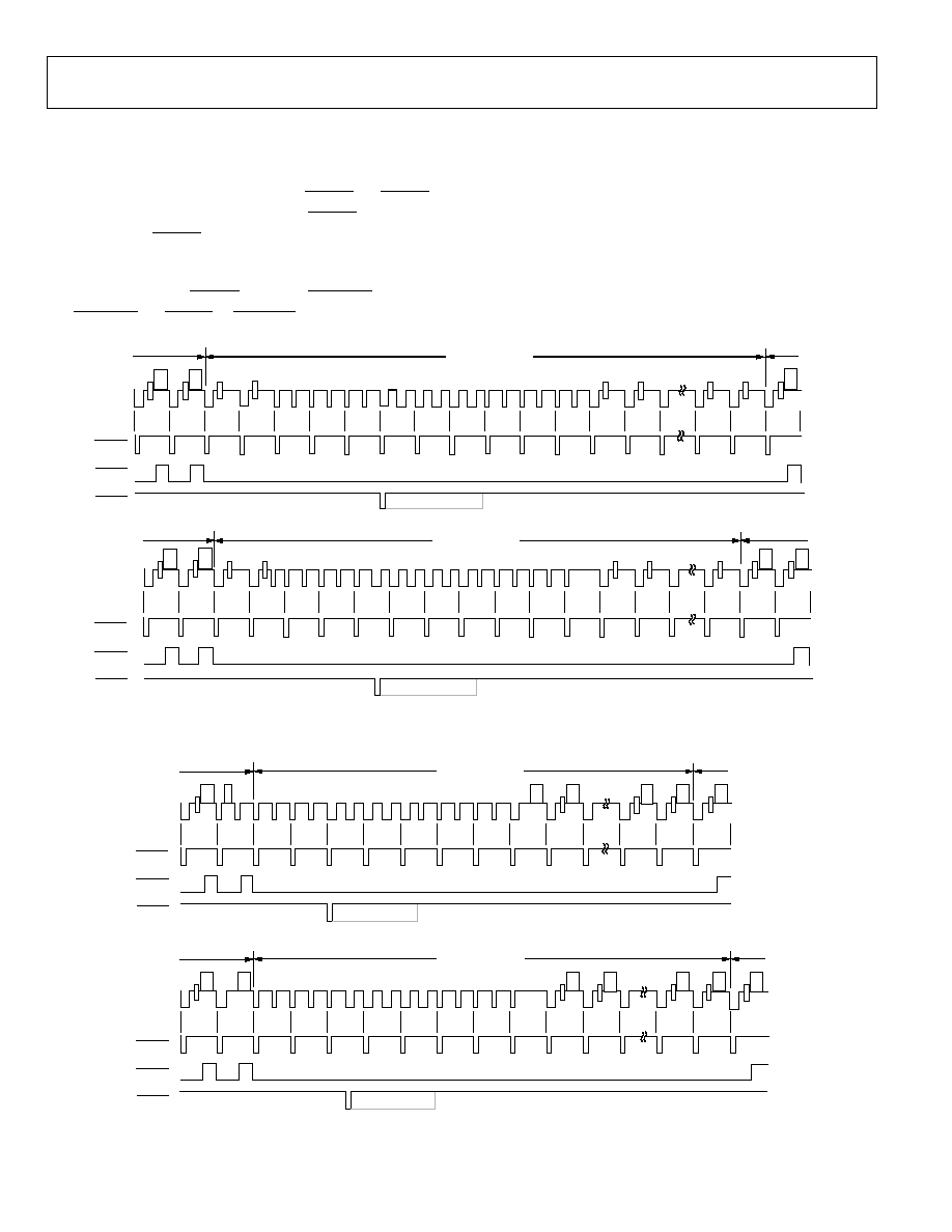
ADV7322
Preliminary Technical Data
Rev. PrA | Page 78 of 88
MODE 2-- SLAVE OPTION
(TIMING REGISTER 0 TR0 = X X X X X 1 0 0)
In this mode, the ADV7322 accepts horizontal and vertical sync
signals. A coincident low transition of both HSYNC and VSYNC
inputs indicates the start of an odd field. A VSYNC low
transition when HSYNC is high indicates the start of an even
field. The BLANK signal is optional. When the BLANK input is
disabled, ADV7322 automatically blanks all normally blank
lines as per CCIR-624. HSYNC is input on S_HSYNC, BLANK
on S_BLANK, andVSYNC on S_VSYNC.
522
523
524
525
9
10
11
20
21
22
DISPLAY
DISPLAY
VERTICAL BLANK
ODD FIELD
EVEN FIELD
260
261
262
263
264
265
266
267
268
269
270
271
272
273
274
283
284
285
ODD FIELD
EVEN FIELD
DISPLAY
DISPLAY
VERTICAL BLANK
5
7
6
4
3
2
1
8
HSYNC
BLANK
VSYNC
HSYNC
BLANK
VSYNC
05067-116
Figure 115. SD Slave Mode 2 (NTSC)
622
623
624
625
21
22
23
DISPLAY
VERTICAL BLANK
ODD FIELD
EVEN FIELD
DISPLAY
309
310
311
312
313
314
315
316
317
318
319
334
335
336
DISPLAY
VERTICAL BLANK
ODD FIELD
EVEN FIELD
DISPLAY
320
7
6
5
4
3
2
1
HSYNC
BLANK
VSYNC
HSYNC
BLANK
VSYNC
05067-117
Figure 116. SD Slave Mode 2 (PAL)
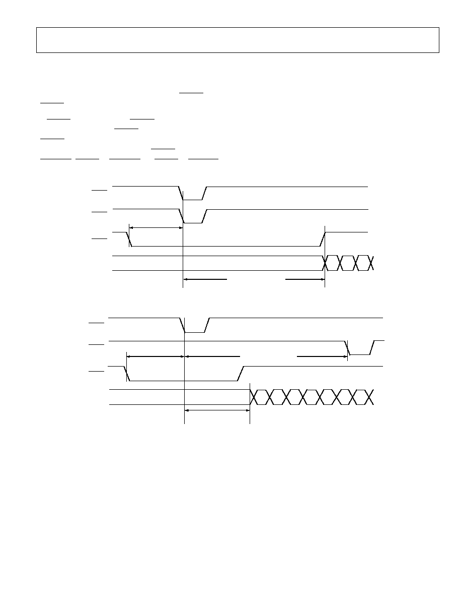
Preliminary Technical Data
ADV7322
Rev. PrA | Page 79 of 88
MODE 2--MASTER OPTION
(TIMING REGISTER 0 TR0 = X X X X X 1 0 1)
In this mode, the ADV7322 can generate horizontal and vertical
sync signals. A coincident low transition of both HSYNC and
VSYNC inputs indicates the start of an odd field.
A VSYNC low transition when HSYNC is high indicates the
start of an even field. The BLANK signal is optional. When the
BLANK input is disabled, the ADV7322 automatically blanks all
normally blank lines as per CCIR-624. HSYNC is output on
S_HSYNC , BLANK on S_BLANK, and VSYNC on S_VSYNC.
Cb
Y
05067-118
PIXEL
DATA
HSYNC
BLANK
VSYNC
PAL = 12
×
CLOCK/2
NTSC = 16
×
CLOCK/2
PAL = 132
×
CLOCK/2
NTSC = 122
×
CLOCK/2
Y
Cr
Figure 117. SD Timing Mode 2 Even-to-Odd Field Transition Master/Slave
Cb
PIXEL
DATA
HSYNC
BLANK
VSYNC
PAL = 12
×
CLOCK/2
NTSC = 16
×
CLOCK/2
PAL = 132
×
CLOCK/2
NTSC = 122
×
CLOCK/2
PAL = 864
×
CLOCK/2
NTSC = 858
×
CLOCK/2
Cb
Y
Y
Cr
05067-119
Figure 118. SD Timing Mode 2 Odd-to-Even Field Transition
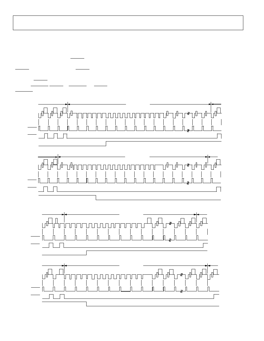
ADV7322
Preliminary Technical Data
Rev. PrA | Page 80 of 88
MODE 3--MASTER/SLAVE OPTION
(TIMING REGISTER 0 TR0 = X X X X X 1 1 0 OR
X X X X X 1 1 1)
In this mode, the ADV7322 accepts or generates horizontal sync
and odd/even field signals. When HSYNC is high, a transition
of the field input indicates a new frame, i.e., vertical retrace. The
BLANK signal is optional. When the BLANK input is disabled,
ADV7322 automatically blanks all normally blank lines as per
CCIR-624. HSYNC is output in master mode and input in slave
mode on S_VSYNC, BLANK on S_BLANK, andVSYNC on
S_VSYNC.
260
261
262
263
264
265
266
267
268
269
270
271
272
273
274
283
284
285
ODD FIELD
EVEN FIELD
DISPLAY
DISPLAY
VERTICAL BLANK
522
523
524
525
9
10
11
20
21
22
DISPLAY
DISPLAY
VERTICAL BLANK
ODD FIELD
EVEN FIELD
HSYNC
BLANK
FIELD
05067-120
HSYNC
BLANK
FIELD
8
7
6
5
4
3
2
1
Figure 119. SD Timing Mode 3 (NTSC)
622
623
624
625
5
6
21
22
23
DISPLAY
VERTICAL BLANK
ODD FIELD
EVEN FIELD
FIELD
DISPLAY
309
310
311
312
313
314
315
316
317
318
319
334
335
336
DISPLAY
VERTICAL BLANK
ODD FIELD
EVEN FIELD
FIELD
DISPLAY
320
4
3
2
1
7
HSYNC
BLANK
HSYNC
BLANK
05067-121
Figure 120. SD Timing Mode 3 (PAL)
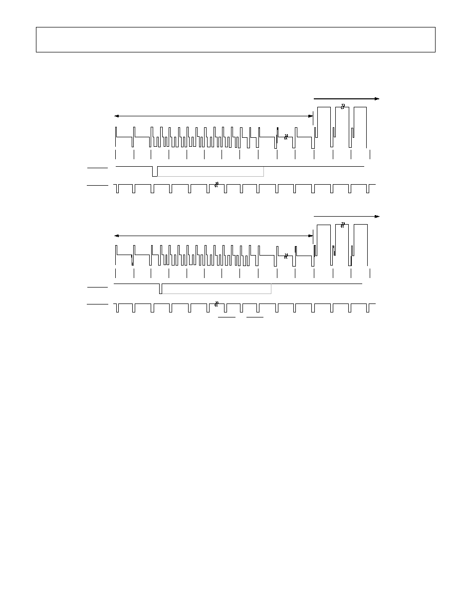
Preliminary Technical Data
ADV7322
Rev. PrA | Page 81 of 88
APPENDIX 6--HD TIMING
VERTICAL BLANKING INTERVAL
DISPLAY
1124
1125
1
2
5
6
7
8
21
4
3
20
22
560
FIELD 1
FIELD 2
VERTICAL BLANKING INTERVAL
DISPLAY
561
562
563
564
567
568
569
570
584
566
565
583
585
1123
P_HSYNC
P_VSYNC
P_HSYNC
P_VSYNC
05067-122
Figure 121. 1080i HSYNC and VSYNC Input Timing
ADV7322
Preliminary Technical Data
Rev. PrA | Page 82 of 88
APPENDIX 7--VIDEO OUTPUT LEVELS
HD YPrPb OUTPUT LEVELS
INPUT CODE
940
64
EIA-770.2, STANDARD FOR Y
OUTPUT VOLTAGE
300mV
700mV
700mV
960
64
EIA-770.2, STANDARD FOR Pr/Pb
OUTPUT VOLTAGE
512
05067-123
Figure 122. EIA 770.2 Standard Output Signals (525p/625p)
782mV
714mV
286mV
700mV
INPUT CODE
940
64
EIA-770.1, STANDARD FOR Y
OUTPUT VOLTAGE
960
64
EIA-770.1, STANDARD FOR Pr/Pb
OUTPUT VOLTAGE
512
05067-124
Figure 123. EIA 770.1 Standard Output Signals (525p/625p)
300mV
INPUT CODE
940
64
EIA-770.3, STANDARD FOR Y
OUTPUT VOLTAGE
700mV
700mV
600mV
960
64
EIA-770.3, STANDARD FOR Pr/Pb
OUTPUT VOLTAGE
512
05067-125
Figure 124. EIA 770.3 Standard Output Signals (1080i/720p)
300mV
300mV
700mV
700mV
INPUT CODE
1023
64
YOUTPUT LEVELS FOR
FULL INPUT SELECTION
OUTPUT VOLTAGE
1023
64
Pr/PbOUTPUT LEVELS FOR
FULL INPUT SELECTION
OUTPUT VOLTAGE
INPUT CODE
05067-126
Figure 125. Output Levels for Full Input Selection
Preliminary Technical Data
ADV7322
Rev. PrA | Page 83 of 88
RGB OUTPUT LEVELS
Pattern: 100%/75% Color Bars
300mV
300mV
300mV
700mV
700mV
525mV
525mV
700mV
525mV
05067-127
Figure 126. PS RGB Output Levels
300mV
0mV
300mV
0mV
300mV
0mV
700mV
525mV
700mV
525mV
700mV
525mV
05067-128
Figure 127. PS RGB Output Levels--RGB Sync Enabled
300mV
300mV
300mV
700mV
700mV
525mV
525mV
700mV
525mV
05067-129
Figure 128. SD RGB Output Levels--RGB Sync Disabled
300mV
0mV
300mV
0mV
300mV
0mV
700mV
525mV
700mV
525mV
700mV
525mV
05067-130
Figure 129. SD RGB Output Levels--RGB Sync Enabled
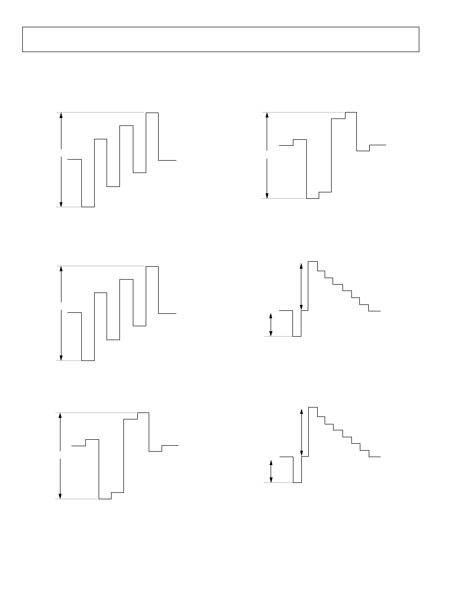
ADV7322
Preliminary Technical Data
Rev. PrA | Page 84 of 88
YPrPb LEVELS--SMPTE/EBU N10
Pattern: 100% Color Bars
WHI
T
E
YELLOW
CY
AN
GR
EEN
MAG
E
NTA
RE
D
BLUE
BLACK
700mV
05067-131
Figure 130. Pb Levels--NTSC
WHI
T
E
YELLOW
CY
AN
GR
EEN
MAG
E
NTA
RE
D
BLUE
BLACK
700mV
0
5
0
6
7
-
1
3
2
Figure 131. Pb Levels--PAL
WHI
T
E
YELLOW
CY
AN
GR
EEN
MAG
E
NT
A
RE
D
BLUE
BLACK
700mV
05067-133
Figure 132. Pr Levels--NTSC
WHI
T
E
YELLOW
CY
AN
GR
EEN
MAG
E
NT
A
RE
D
BLUE
BLACK
700mV
05067-134
Figure 133. Pr Levels--PAL
300mV
700mV
WHI
T
E
YELLOW
CY
AN
GR
EEN
MAG
E
NT
A
RE
D
BLUE
BLACK
05067-135
Figure 134. Y Levels--NTSC
700mV
300mV
WHI
T
E
YELLOW
CY
AN
GR
EEN
MAG
E
NT
A
RE
D
BLUE
BLACK
05067-136
Figure 135. Y Levels--PAL
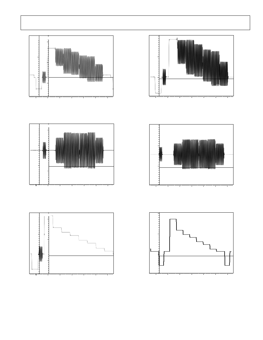
Preliminary Technical Data
ADV7322
Rev. PrA | Page 85 of 88
0.5
0
APL = 44.5%
525 LINE NTSC
SLOW CLAMP TO 0.00V AT 6.72
µ
s
10
20
F1
L76
30
40
50
60
100
50
0
50
0
VOLTS IRE:FLT
MICROSECONDS
PRECISION MODE OFF
SYNCHRONOUS SYNC = A
FRAMES SELECTED 1, 2
05067-137
Figure 136. NTSC Color Bars 75%
05067-138
0
NOISE REDUCTION: 15.05dB
APL NEEDS SYNC-SOURCE.
525 LINE NTSC NO FILTERING
SLOW CLAMP TO 0.00 AT 6.72
µ
s
10
20
F1
L76
30
40
50
60
50
50
0
0.4
0.2
0
0.2
0.4
MICROSECONDS
PRECISION MODE OFF
SYNCHRONOUS SYNC = B
FRAMES SELECTED 1, 2
VOLTS IRE:FLT
Figure 137. NTSC Chroma
05067-139
NOISE REDUCTION: 15.05dB
APL = 44.3%
525 LINE NTSC NO FILTERING
SLOW CLAMP TO 0.00 AT 6.72
µ
s
10
20
F2
L238
30
40
50
60
50
0
0
0.4
0.2
0.6
0
0.2
MICROSECONDS
PRECISION MODE OFF
SYNCHRONOUS SYNC = SOURCE
FRAMES SELECTED 1, 2
VOLTS IRE:FLT
Figure 138. NTSC Luma
05067-140
VOLTS
NOISE REDUCTION: 0.00dB
APL = 39.1%
625 LINE NTSC NO FILTERING
SLOW CLAMP TO 0.00 AT 6.72
µ
s
10
0
20
L608
30
40
50
60
0.4
0.2
0.6
0
0.2
MICROSECONDS
PRECISION MODE OFF
SYNCHRONOUS SOUND-IN-SYNC OFF
FRAMES SELECTED 1, 2, 3, 4
Figure 139. PAL Color Bars 75%
05067-141
VOLTS
APL NEEDS SYNC-SOURCE.
625 LINE PAL NO FILTERING
SLOW CLAMP TO 0.00 AT 6.72
µ
s
10
20
L575
30
40
50
60
0
0.5
0.5
MICROSECONDS NO BUNCH SIGNAL
PRECISION MODE OFF
SYNCHRONOUS SOUND-IN-SYNC OFF
FRAMES SELECTED 1
Figure 140. PAL Chroma
05067-142
VOLTS
APL NEEDS SYNC-SOURCE.
625 LINE PAL NO FILTERING
SLOW CLAMP TO 0.00 AT 6.72
µ
s
10
0
20
L575
30
40
50
60
0
0.5
MICROSECONDS NO BUNCH SIGNAL
PRECISION MODE OFF
SYNCHRONOUS SOUND-IN-SYNC OFF
FRAMES SELECTED 1
70
Figure 141. PAL Luma
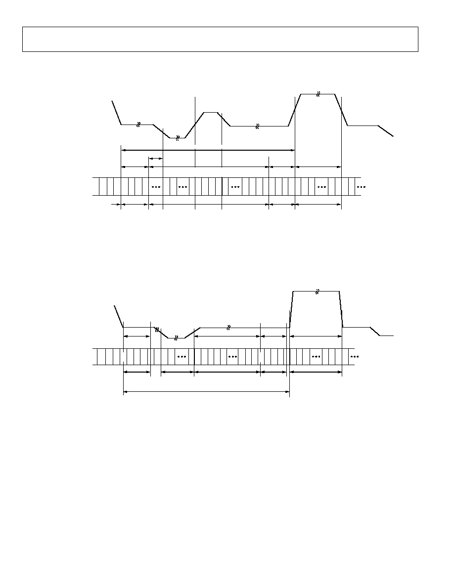
ADV7322
Preliminary Technical Data
Rev. PrA | Page 86 of 88
APPENDIX 8--VIDEO STANDARDS
F
V
H*
F
F
272T
4T
*1
4T
1920T
EAV CODE
SAV CODE
DIGITAL
ACTIVE LINE
4 CLOCK
4 CLOCK
2112
2116 2156
2199
0
44
188
192
2111
0
0
0
0
0
0
0
0
F
F
F
V
H*
C
b
C
r
C
r
Y
Y
FVH* = FVH AND PARITY BITS
SAV/EAV: LINE 1562: F = 0
SAV/EAV: LINE 5631125: F = 1
SAV/EAV: LINE 120; 561583; 11241125: V = 1
SAV/EAV: LINE 21560; 5841123: V = 0
FOR A FRAME RATE OF 30Hz: 40 SAMPLES
FOR A FRAME RATE OF 25Hz: 480 SAMPLES
INPUT PIXELS
ANALOG WAVEFORM
SAMPLE NUMBER
SMPTE 274M
DIGITAL HORIZONTAL BLANKING
ANCILLARY DATA
(OPTIONAL) OR BLANKING CODE
0
H
DATUM
05067-143
Figure 142. EAV/SAV Input Data Timing Diagram--SMPTE 274M
Y
EAV CODE
ANCILLARY DATA
(OPTIONAL)
SAV CODE
DIGITAL
ACTIVE LINE
719
723 736
799
853
0
FVH* = FVH AND PARITY BITS
SAV: LINE 43525 = 200H
SAV: LINE 142 = 2AC
EAV: LINE 43525 = 274H
EAV: LINE 142 = 2D8
4 CLOCK
4 CLOCK
857
719
0
H
DATUM
DIGITAL HORIZONTAL BLANKING
0
0
0
0
0
0
0
0
C
b
C
r
C
r
Y
Y
F
V
H*
SMPTE 293M
INPUT PIXELS
ANALOG WAVEFORM
SAMPLE NUMBER
F
F
F
F
F
V
H*
05067-144
Figure 143. EAV/SAV Input Data Timing Diagram--SMPTE 293M
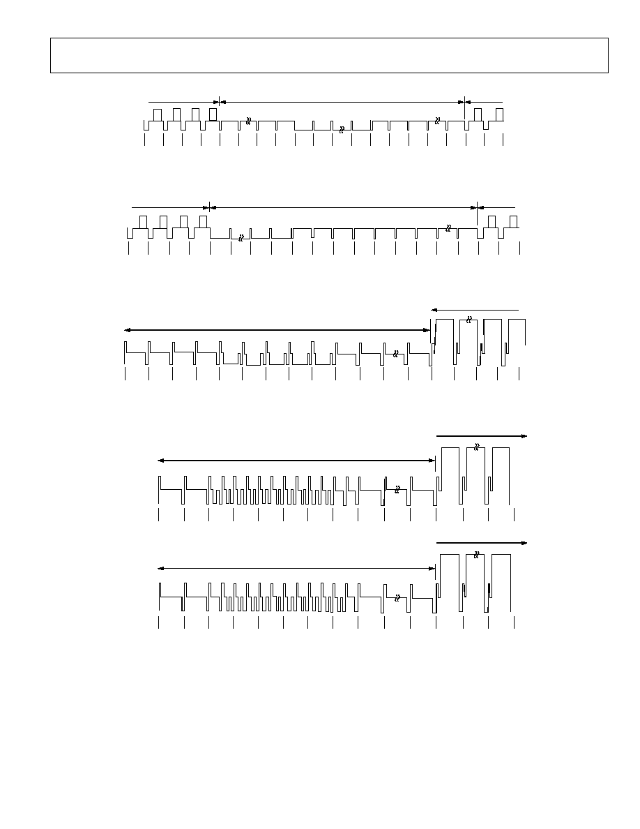
Preliminary Technical Data
ADV7322
Rev. PrA | Page 87 of 88
VERTICAL BLANK
522
523
524
525
1
2
5
6
7
8
9
12
13
14
15
16
42
43
44
ACTIVE
VIDEO
ACTIVE
VIDEO
05067-145
Figure 144. SMPTE 293M (525p)
622
623
624
625
10
11
43
44
45
4
VERTICAL BLANK
ACTIVE
VIDEO
ACTIVE
VIDEO
1
2
5
6
7
8
9
12
13
05067-146
Figure 145. ITU-R BT.1358 (625p)
747
748
749
750
26
27
25
744
745
DISPLAY
VERTICAL BLANKING INTERVAL
1
2
3
4
5
6
7
8
05067-147
Figure 146. SMPTE 296M (720p)
DISPLAY
1124
1125
21
4
3
20
22
560
FIELD 1
DISPLAY
561
562
563
564
567
568
569
570
584
566
565
583
585
1123
FIELD 2
VERTICAL BLANKING INTERVAL
VERTICAL BLANKING INTERVAL
1
2
5
6
7
8
05067-148
Figure 147. SMPTE 274M (1080i)
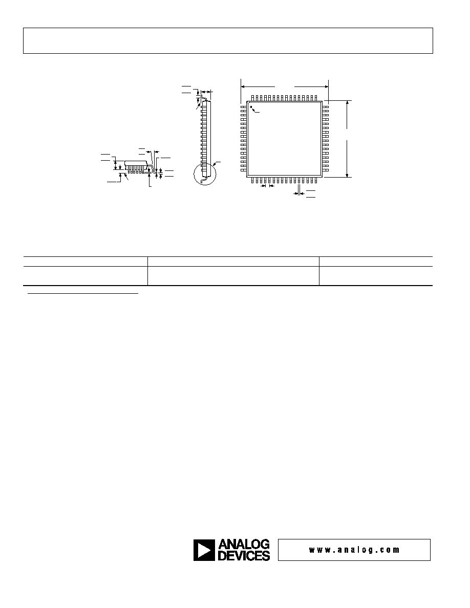
ADV7322
Preliminary Technical Data
Rev. PrA | Page 88 of 88
OUTLINE DIMENSIONS
TOP VIEW
(PINS DOWN)
1
16
17
33
32
48
49
64
0.27
0.22
0.17
0.50
BSC
10.00
BSC SQ
1.60
MAX
SEATING
PLANE
0.75
0.60
0.45
VIEW A
12.00
BSC SQ
0.20
0.09
1.45
1.40
1.35
0.08 MAX
COPLANARITY
VIEW A
ROTATED 90° CCW
SEATING
PLANE
10°
6°
2°
7°
3.5°
0°
0.15
0.05
PIN 1
COMPLIANT TO JEDEC STANDARDS MS-026BCD
Figure 148. 64-Lead Low Profile Quad Flat Package [LQFP]
(ST-64-2)
Dimensions shown in millimeters
ORDERING GUIDE
Model
Package Description
Package Option
ADV7322KSTZ
1
64-Lead Low Profile Quad Flat Package [LQFP]
ST-64-2
EVAL-ADV7322EB
Evaluation Board
1
Z = Pb-free part.
© 2004 Analog Devices, Inc. All rights reserved. Trademarks and
registered trademarks are the property of their respective owners.
PR0513509/04(PrA)
Document Outline