 | ÐлекÑÑоннÑй компоненÑ: ADV7324 | СкаÑаÑÑ:  PDF PDF  ZIP ZIP |
Äîêóìåíòàöèÿ è îïèñàíèÿ www.docs.chipfind.ru
Multiformat 216 MHz
Video Encoder with Six NSV
®
14-Bit DACs
ADV7324
Rev. 0
Information furnished by Analog Devices is believed to be accurate and reliable.
However, no responsibility is assumed by Analog Devices for its use, nor for any
infringements of patents or other rights of third parties that may result from its use.
Specifications subject to change without notice. No license is granted by implication
or otherwise under any patent or patent rights of Analog Devices. Trademarks and
registered trademarks are the property of their respective owners.
One Technology Way, P.O. Box 9106, Norwood, MA 02062-9106, U.S.A.
Tel: 781.329.4700
www.analog.com
Fax: 781.326.8703
© 2004 Analog Devices, Inc. All rights reserved.
FEATURES
High definition (HD) input formats
16-/20-, 24-/30-bit (4:2:2, 4:4:4) parallel YCrCb
Fully compliant with:
SMPTE 274M (1080i, 1080p @ 74.25 MHz)
SMPTE 296M (720p)
SMPTE 240M (1035i)
RGB in 3-bit × 10-bit 4:4:4 input format
HDTV RGB supported:
RGB, RGBHV
Other HD formats using async
timing mode
Enhanced definition (ED) input formats
8-/10-, 16-/20-, 24-/30-bit (4:2:2, 4:4:4) parallel YCrCb
SMPTE 293M (525p)
BTA T-1004 EDTV2 (525p)
ITU-R BT.1358 (625p/525p)
ITU-R BT.1362 (625p/525p)
RGB in 3-bit × 10-bit 4:4:4 input format
Standard definition (SD) input formats
CCIR-656 4:2:2 8-/10-bit or 16-/20-bit parallel input
HD output formats
YPrPb HDTV (EIA 770.3)
RGB, RGBHV
CGMS-A (720p/1080i)
ED output formats
Macrovision Rev 1.2 (525p/625p)
CGMS-A (525p/625p)
YPrPb progressive scan (PS) (EIA-770.1, EIA-770.2)
RGB, RGBHV
SD output formats
Composite NTSC M/N
Composite PAL M/N/B/D/G/H/I, PAL-60
SMPTE 170M NTSC-compatible composite video
ITU-R BT.470 PAL-compatible composite video
S-video (Y/C)
EuroScart RGB
Component YPrPb (Betacam, MII, SMPTE/EBU N10)
Macrovision Rev 7.1.L1
CGMS/WSS
Closed captioning
GENERAL FEATURES
Simultaneous SD/HD or PS/SD inputs and outputs
Oversampling up to 216 MHz
Programmable DAC gain control
Sync outputs in all modes
On-board voltage reference
Six 14-bit NSV (noise shaped video) precision video DACs
2-wire serial I
2
C® interface, open-drain configuration
Dual I/O supply 2.5 V/3.3 V operation
Analog and digital supply 2.5 V
On-board PLL
64-lead LQFP package
Lead (Pb) free product
APPLICATIONS
EVD (enhanced versatile disk) players
High-end SD/PS DVD recorders/players
SD/PS/HDTV display devices
SD/HDTV set top boxes
Professional video systems
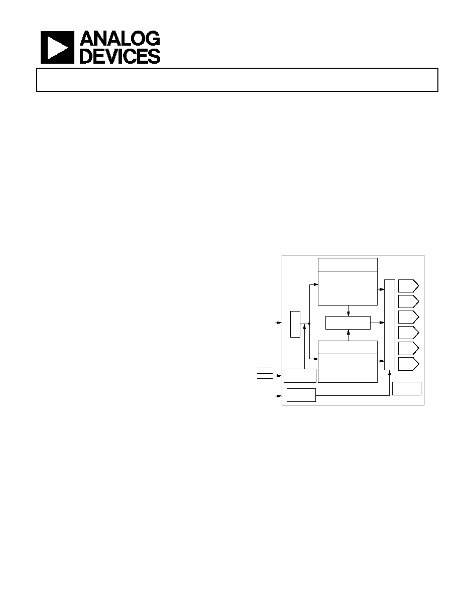
CLKIN_A
CLKIN_B
HSYNC
VSYNC
BLANK
Y9Y0
C9C0
S9S0
TIMING
GENERATOR
PLL
O
V
E
R
S
A
M
P
L
I
N
G
I
2
C
INTERFACE
D
E
M
U
X
SD
CONTROL BLOCK
COLOR CONTROL
BRIGHTNESS
DNR
GAMMA
PROGRAMMABLE
FILTERS
SD TEST PATTERN
HD
CONTROL BLOCK
HD TEST PATTERN
COLOR CONTROL
ADAPTIVE FILTER CTRL
SHARPNESS FILTER
PROGRAMMABLE
RGB MATRIX
14-BIT
DAC
14-BIT
DAC
14-BIT
DAC
14-BIT
DAC
14-BIT
DAC
14-BIT
DAC
ADV7324
05220-001
Figure 1. Simplified Functional Block Diagram
GENERAL DESCRIPTION
The ADV®7324 is a high speed, digital-to-analog encoder on a
single monolithic chip. It includes six high speed NSV video
DACs with TTL-compatible inputs. It has separate 8-/10-,
16-/20-, and 24-/30-bit input ports that accept data in high
definition (HD) and/or standard definition (SD) video format.
For all standards, external horizontal, vertical, and blanking
signals, or EAV/SAV timing codes, control the insertion of
appropriate synchronization signals into the digital data stream
and, therefore, the output signal.

ADV7324
Rev. 0 | Page 2 of 92
TABLE OF CONTENTS
Specifications..................................................................................... 6
Dynamic Specifications ............................................................... 7
Timing Specifications .................................................................. 8
Timing Diagrams.............................................................................. 9
Absolute Maximum Ratings.......................................................... 16
Thermal Characteristics ............................................................ 16
ESD Caution................................................................................ 16
Pin Configuration and Function Descriptions........................... 17
Typical Performance Characteristics ........................................... 19
MPU Port Description................................................................... 23
Register Access................................................................................ 25
Register Programming............................................................... 25
Subaddress Registers (SR7 to SR0)........................................... 25
Input Configuration ....................................................................... 38
SD Only........................................................................................ 38
PS Only or HDTV Only ............................................................ 38
Simultaneous SD/PS or SD/HDTV.......................................... 38
PS at 27 MHz (Dual Edge) or 54 MHz .................................... 39
Features ............................................................................................ 41
Output Configuration................................................................ 41
HD Async Timing Mode ........................................................... 42
HD Timing Reset........................................................................ 43
SD Real-Time Control, Subcarrier Reset, and
Timing Reset ............................................................................... 43
Reset Sequence............................................................................ 45
SD VCR FF/RW Sync................................................................. 45
Vertical Blanking Interval ......................................................... 46
Subcarrier Frequency Registers ................................................ 46
Square Pixel Timing Mode........................................................ 47
Filters............................................................................................ 48
Color Controls and RGB Matrix .............................................. 49
Programmable DAC Gain Control .......................................... 53
Gamma Correction .................................................................... 53
HD Sharpness Filter and Adaptive Filter Controls................ 55
HD Sharpness Filter and Adaptive Filter
Application Examples ................................................................ 56
SD Digital Noise Reduction...................................................... 57
Coring Gain Border ................................................................... 58
Coring Gain Data ....................................................................... 58
DNR Threshold .......................................................................... 58
Border Area................................................................................. 58
Block Size Control...................................................................... 58
DNR Input Select Control......................................................... 58
DNR Mode Control ................................................................... 59
Block Offset Control .................................................................. 59
SD Active Video Edge................................................................ 59
SAV/EAV Step-Edge Control ................................................... 59
Hsync/Vsync Output Control .................................................. 61
Board Design and Layout.............................................................. 62
DAC Termination and Layout Considerations ...................... 62
Video Output Buffer and Optional Output Filter.................. 62
PCB Board Layout...................................................................... 63
Appendix 1--Copy Generation Management System .............. 65
PS CGMS..................................................................................... 65
HD CGMS................................................................................... 65
SD CGMS .................................................................................... 65
CGMS Functionality.................................................................. 65
Appendix 2--SD Wide-Screen Signaling.................................... 68
Appendix 3--SD Closed Captioning ........................................... 70
Appendix 4--Test Patterns............................................................ 71
Appendix 5--SD Timing Modes .................................................. 74
Mode 0 (CCIR-656)--Slave Option
(Timing Register 0 TR0 = X X X X X 0 0 0) ........................... 74
Mode 0 (CCIR-656)--Master Option
(Timing Register 0 TR0 = X X X X X 0 0 1) ........................... 75

ADV7324
Rev. 0 | Page 3 of 92
Mode 1--Slave Option
(Timing Register 0 TR0 = X X X X X 0 1 0) ............................77
Mode 1--Master Option
(Timing Register 0 TR0 = X X X X X 0 1 1) ............................78
Mode 2-- Slave Option
(Timing Register 0 TR0 = X X X X X 1 0 0) ............................79
Mode 2--Master Option
(Timing Register 0 TR0 = X X X X X 1 0 1) ............................80
Mode 3--Master/Slave Option
(Timing Register 0 TR0 = X X X X X 1 1 0 or X X X X X 1 1 1)
.......................................................................................................81
Appendix 6--HD Timing ..............................................................82
Appendix 7--Video Output Levels...............................................83
HD YPrPb Output Levels ..........................................................83
RGB Output Levels .....................................................................84
YPrPb Levels--SMPTE/EBU N10............................................85
Appendix 8--Video Standards ......................................................87
Outline Dimensions........................................................................89
Ordering Guide ...........................................................................89
REVISION HISTORY
11/04--Revision 0: Initial Version
ADV7324
Rev. 0 | Page 4 of 92
DETAILED FEATURES
HD programmable features (720p/1080i/1035i)
2× oversampling (148.5 MHz)
Internal test pattern generator
Color hatch, black bar, flat field/frame
Fully programmable YCrCb to RGB matrix
Gamma correction
Programmable adaptive filter control
Programmable sharpness filter control
CGMS-A (720p/1080i)
ED programmable features (525p/625p)
8× oversampling (216 MHz output)
Internal test pattern generator
Color hatch, black bar, flat frame
Individual Y and PrPb output delay
Gamma correction
Programmable adaptive filter control
Fully programmable YCrCb to RGB matrix
Undershoot limiter
Macrovision Rev 1.2 (525p/625p)
CGMS-A (525p/625p)
SD programmable features
16× oversampling (216 MHz)
Internal test pattern generator
Color bars, black bar
Controlled edge rates for start and end of active video
Individual Y and PrPb output delay
Undershoot limiter
Gamma correction
Digital noise reduction (DNR)
Multiple chroma and luma filters
Luma-SSAFTM filter with programmable gain/attenuation
PrPb SSAFTM
Separate pedestal control on component and
composite/S-video output
VCR FF/RW sync mode
Macrovision Rev 7.1.L1
CGMS/WSS
Closed captioning
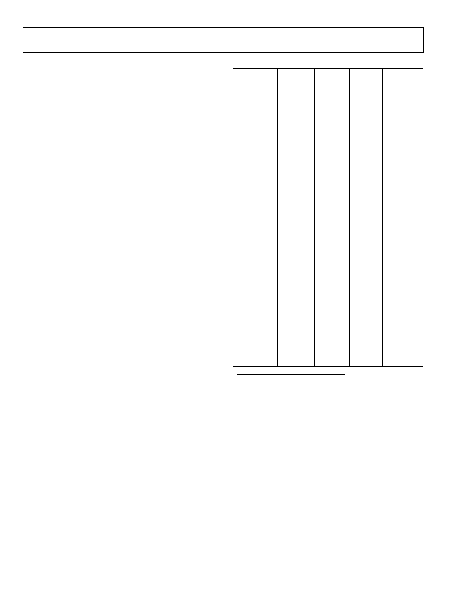
Table 1. Standards Directly Supported
1
Resolution
Interlace/
PS
Frame
Rate
(Hz)
Clock
Input
(MHz)
Standard
720 × 480
I
29.97
27
ITU-R
BT.656
720 × 576
I
25
27
ITU-R
BT.656
720 × 480
I
29.97
24.54
NTSC
Square
Pixel
720 × 576
I
25
29.5
PAL Square
Pixel
720 × 483
P
59.94
27
SMPTE
293M
720 × 483
P
59.94
27
BTA T-1004
720 × 483
P
59.94
27
ITU-R
BT.1358
720 × 576
P
50
27
ITU-R
BT.1358
720 × 483
P
59.94
27
ITU-R
BT.1362
720 × 576
P
50
27
ITU-R
BT.1362
30 74.25
1920 × 1035
I
29.97 74.1758
SMPTE
240M
60, 50,
30, 25, 24
74.25
1280 × 720
P
23.97,
59.94,
29.97
74.1758
SMPTE
296M
30, 25
74.25
1920 × 1080
I
29.97 74.1758
SMPTE
274M
30, 25, 24
74.25
1920 × 1080
P
23.98,
29.97
74.1758
SMPTE
274M
1
Other standards are supported in async timing mode.
ADV7324
Rev. 0 | Page 5 of 92
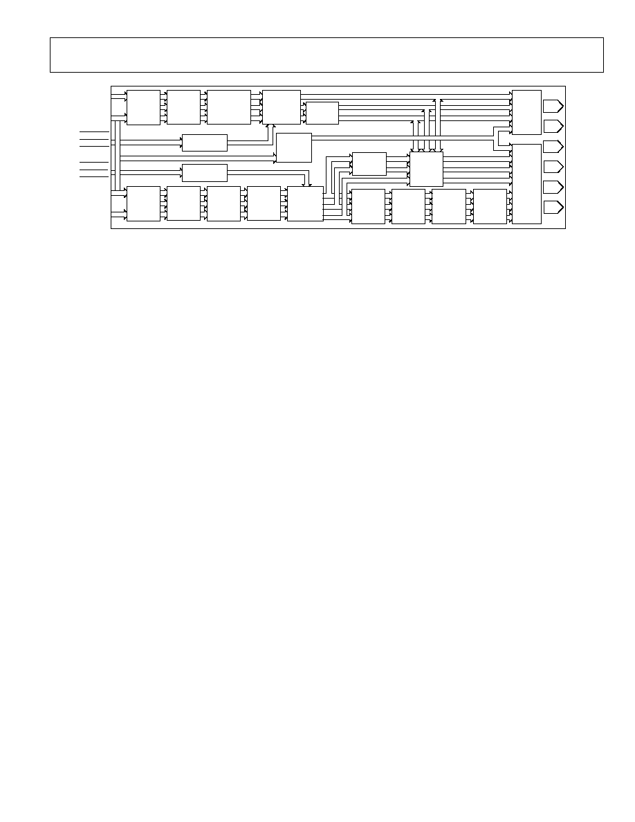
CLKIN_A
P_HSYNC
P_VSYNC
P_BLANK
S_HSYNC
S_VSYNC
S_BLANK
CLKIN_B
HD PIXEL
INPUT
SD PIXEL
INPUT
LUMA
AND
CHROMA
FILTERS
Y
CB
CR
TEST
PATTERN
DNR
GAMMA
SYNC
INSERTION
PS 8
×
HDTV 2
×
RGB
MATRIX
SD 16
×
2
×
OVER-
SAMPLING
DAC
DAC
DAC
DAC
DAC
DAC
F
SC
MODU-
LATION
CGMS
WSS
COLOR
CONTROL
DE-
INTER-
LEAVE
Y
CB
CR
DE-
INTER-
LEAVE
TEST
PATTERN
Y COLOR
CR COLOR
CB COLOR
TIMING
GENERATOR
TIMING
GENERATOR
CLOCK
CONTROL
AND PLL
4:2:2
TO
4:4:4
SHARPNESS
AND
ADAPTIVE
FILTER
CONTROL
05220-002
UV SSAF
V
U
Figure 2. Detailed Functional Block Diagram
TERMINOLOGY
SD: standard definition video, conforming to
ITU-R BT.601/ITU-R BT.656.
HD: high definition video, i.e., 720p/1080i/1035i.
EDTV: enhanced definition television (525p/625p).
PS: progressive scan video, conforming to SMPTE 293M,
ITU-R BT.1358, BTA T-1004 EDTV2, or ITU-R BT.13621362.
HDTV: high definition television video, conforming to
SMPTE 274M, or SMPTE 296M and SMPTE 240M.
YCrCb SD, PS, or HD component: digital video.
YPrPb SD, PS, or HD component: analog video.
Document Outline