Äîêóìåíòàöèÿ è îïèñàíèÿ www.docs.chipfind.ru

ADV7400A
Rev. A | Page 3 of 16
ELECTRICAL CHARACTERISTICS
A
VDD
= 3.15 V to 3.45 V, D
VDD
= 1.65 V to 2.0 V, D
VDDIO
= 3.0 V to 3.6 V, P
VDD
= 1.65 V to 2.0 V, nominal input range = 1.6 V, operating
temperature range, unless otherwise noted.
Table 1. Electrical Characteristics
1,2
Parameter Symbol
Test
Conditions
Min
Typ
Max
Unit
STATIC PERFORMANCE
3
Resolution (each ADC)
N
10
Bits
Integral Nonlinearity
INL
BSL at 27 MHz (at a 10-bit level)
±0.6
±2.5
LSB
Integral Nonlinearity
INL
BSL at 54 MHz (at a 10-bit level)
-0.6/+0.7
LSB
Integral Nonlinearity
INL
BSL at 74 MHz (at a 10-bit level)
-1.2/+1.5
LSB
Integral Nonlinearity
INL
BSL at 110 MHz (at an 8-bit level)
4
-0.9/+1.6
LSB
Differential Nonlinearity
DNL
At 27 MHz (at a 10-bit level)
-0.2/+0.25
-0.3/+0.7
LSB
Differential Nonlinearity
DNL
At 54 MHz (at a 10-bit level)
-0.2/+0.25
LSB
Differential Nonlinearity
DNL
At 74 MHz (at a 10-bit level)
±0.8
LSB
Differential Nonlinearity
DNL
At 110 MHz (at an 8-bit level)
4
-0.2/+1.5
LSB
DIGITAL INPUTS
Input High Voltage
V
IH
2
V
Input Low Voltage
V
IL
0.8
V
XTAL High Voltage
V
IH
Pin 38
1.2
V
XTAL Low Voltage
V
IL
Pin 38
0.4
V
Input High Voltage
V
IH
HS_IN, VS_IN low trigger mode
0.7
V
Input Low Voltage
V
IL
HS_IN, VS_IN low trigger mode
0.4
V
Input Current
I
IN
Pins listed in Note 5
-60
+60
µA
All other input pins
-10
+10
µA
Input Capacitance
6
C
IN
10
pF
DIGITAL OUTPUTS
Output High Voltage
V
OH
I
SOURCE
= 0.4 mA
2.4
V
Output Low Voltage
V
OL
I
SINK
= 3.2 mA
0.4
V
High Impedance Leakage Current
I
LEAK
Pins listed in Note 7
60
µA
All other output pins
10
µA
Output Capacitance
6
C
OUT
20
pF
POWER REQUIREMENTS
6
Digital Core Power Supply
D
VDD
1.65
1.8
2
V
Digital I/O Power Supply
D
VDDIO
3.0
3.3
3.6
V
PLL Power Supply
P
VDD
1.65
1.8
2
V
Analog Power Supply
A
VDD
3.15
3.3
3.45
V
Digital Core Supply Current
I
DVDD
CVBS input sampling at 54 MHz
82
mA
Graphics RGB sampling at 110 MHz
4
62
mA
Digital I/O Supply Current
I
DVDDIO
CVBS input sampling at 54 MHz
2
mA
Graphics RGB sampling at 110 MHz
4
17
mA
PLL Supply Current
I
PVDD
54 MHz
10.5
mA
110
MHz
6
mA
Analog Supply Current
I
AVDD
CVBS input sampling at 54 MHz
85
mA
Graphics RGB sampling at 110 MHz
4
218
mA
Power-Down Current
I
PWRDN
1.5
mA
Green Mode Power-Down
I
PWRDNG
Sync bypass function
12.5
mA
Power-Up Time
T
PWRUP
20
ms
1
The min/max specifications are guaranteed over this range.
2
Temperature range T
MIN
to T
MAX
:
-40°C to +85°C.
3
All ADC linearity tests performed at input range of full scale are
-12.5%, and at zero scale they are +12.5%.
4
Specifications for the ADV7400AKSTZ-110 and the ADV7400ABSTZ-110 only.
5
Pins: 1, 2, 3, 13, 14, 16, 19, 24, 29, 30, 31, 32, 33, 34, 35, 45, 79, 83, 84, 87, 88, 95, 96, 97, 100.
6
Guaranteed by characterization.
7
Pins: 45, 34, 33, 32, 31, 30, 29, 24, 14, 13 (P20 to P29).

ADV7400A
Rev. A | Page 4 of 16
VIDEO SPECIFICATIONS
A
VDD
= 3.15 V to 3.45 V, D
VDD
= 1.65 V to 2.0 V, D
VDDIO
= 3.0 V to 3.6 V, P
VDD
= 1.65 V to 2.0 V, operating temperature range, unless
otherwise noted.
Table 2. Video Specifications
1, ,
2 3
Parameter Symbol
Test
Conditions
Min
Typ
Max
Unit
NONLINEAR SPECIFICATIONS
Differential Phase
DP
CVBS I/P, modulated 5 step
0.5
0.7
degree
Differential Gain
DG
CVBS I/P, modulated 5 step
0.5
0.7
%
Luma Nonlinearity
LNL
CVBS I/P, 5 step
0.5
0.7
%
NOISE SPECIFICATIONS
SNR Unweighted
Luma ramp
54
56
dB
SNR Unweighted
Luma flat field
58
60
dB
Analog Front End Crosstalk
60 dB
LOCK TIME SPECIFICATIONS
Horizontal Lock Range
-5
+5
%
Vertical Lock Range
40
70 Hz
F
SC
Subcarrier Lock Range
±1.3
kHz
Color Lock in Time
60
line
Sync Depth Range
20
200
%
Color Burst Range
5
200
%
Vertical Lock Time
2
field
Horizontal Lock Time
100
line
CHROMA SPECIFICATIONS
Hue Accuracy
HUE
1
degree
Color Saturation Accuracy
CL_AC
1
%
Color AGC Range
5
400
%
Chroma Amplitude Error
0.5
%
Chroma Phase Error
0.4
degree
Chroma Luma Intermodulation
0.2
%
LUMA SPECIFICATIONS
Luma Brightness Accuracy
CVBS, 1 V input
1
%
Luma Contrast Accuracy
CVBS, 1 V input
1
%
1
The min/max specifications are guaranteed over this range.
2
Temperature range T
MIN
to T
MAX
:
-40°C to +85°C.
3
Guaranteed by characterization.

ADV7400A
Rev. A | Page 5 of 16
TIMING CHARACTERISTICS
A
VDD
= 3.15 V to 3.45 V, D
VDD
= 1.65 V to 2.0 V, D
VDDIO
= 3.0 V to 3.6 V, P
VDD
= 1.65 V to 2.0 V, operating temperature range, unless
otherwise noted.
Table 3. Timing Characteristics
1, ,
2 3
Parameter Symbol Test
Conditions
Min
Typ
Max
Unit
SYSTEM CLOCK AND CRYSTAL
Crystal Nominal Frequency
27.0
MHz
Crystal Frequency Stability
±50
ppm
Horizontal Sync Input Frequency
14.8
110
kHz
LLC1 Frequency Range
4
12.825
110
MHz
I
2
C® PORT
SCLK Frequency
400
kHz
SCLK Min Pulse Width High
t
1
0.6
µs
SCLK Min Pulse Width Low
t
2
1.3
µs
Hold Time (Start Condition)
t
3
0.6
µs
Setup Time (Start Condition)
t
4
0.6
µs
SDA Setup Time
t
5
100
ns
SCLK and SDA Rise Time
t
6
300
ns
SCLK and SDA Fall Time
t
7
300
ns
Setup Time for Stop Condition
t
8
0.6
µs
RESET FEATURE
Reset Pulse Width
5
ms
CLOCK OUTPUTS
LLC1 Mark Space Ratio
t
9
:t
10
45:55
55:45
% duty
cycle
DATA and CONTROL OUTPUTS
Data Output Transition Time (SDP)
t
11
Negative clock edge to start of valid data
3.4
ns
Data Output Transition Time (SDP)
t
12
End of valid data to negative clock edge
2.4
ns
Data Output Transition Time (CP)
t
13
End of valid data to negative clock edge
1.1
ns
Data Output Transition Time (CP)
t
14
Negative clock edge to start of valid edge
2.2
ns
Data Output Transition Time DDR (CP)
5
t
15
Positive clock edge to end of valid data
-2.7 + T
LLC1
/4
ns
Data Output Transition Time DDR (CP)
5
t
16
Start of valid data to positive clock edge
-1.3 + T
LLC1
/4
ns
Data Output Transition Time DDR (CP)
5
t
17
Negative clock edge to end of valid data
-2.1 + T
LLC1
/4
ns
Data Output Transition Time DDR (CP)
5
t
18
Start of valid data to negative clock edge
-0.9 + T
LLC1
/4
ns
DATA and CONTROL INPUTS
Input Setup Time
t
19
HS_IN, VS_IN
9
ns
DE_IN, data inputs
2.2
ns
Input Hold Time
t
20
HS_IN, VS_IN
7
ns
DE_IN, data inputs
1
ns
1
The min/max specifications are guaranteed over this range.
2
Temperature range T
MIN
to T
MAX
:
-40°C to +85°C.
3
Guaranteed by characterization.
4
Maximum LLC1 frequency is 80 MHz for the ADV7400AKSTZ-80.
5
DDR timing specifications depend on LLC1 output pixel clock; T
LCC1
/4 = 9.25 ns at LLC1 = 27 MHz.
ADV7400A
Rev. A | Page 6 of 16
ANALOG SPECIFICATIONS
A
VDD
= 3.1.5 V to 3.45 V, D
VDD
= 1.65 V to 2.0 V, D
VDDIO
= 3.0 V to 3.6 V, P
VDD
= 1.65 V to 2.0 V, operating temperature range, unless
otherwise noted.
Table 4. Analog Specifications
1, ,
2 3
Parameter Symbol
Test
Conditions
Min
Typ
Max
Unit
CLAMP CIRCUITRY
External Clamp Capacitor
0.1
µF
Input Impedance
Clamps switched off
10
M
Voltage Clamp Level
1.7
V
Large Clamp Source Current
SDP only
0.75
mA
Large Clamp Sink Current
SDP only
0.75
mA
Fine Clamp Source Current
SDP only
60
µA
Fine Clamp Sink Current
SDP only
60
µA
1
The min/max specifications are guaranteed over this range.
2
Temperature range T
MIN
to T
MAX
:
-40°C to +85°C.
3
Guaranteed by characterization.
THERMAL SPECIFICATIONS
Table 5. Thermal Specifications
Thermal Characteristic
Symbol
Test Conditions
Typ
Unit
Junction-to-Case Thermal Resistance
JC
4-layer PCB with solid ground plane
7
°C/W
Junction-to-Ambient Thermal Resistance
JA
4-layer PCB with solid ground plane (still air)
30
°C/W
ADV7400A
Rev. A | Page 7 of 16
ABSOLUTE MAXIMUM RATINGS
Table 6.
Parameter Rating
A
VDD
to AGND
4 V
D
VDD
to DGND
2.2 V
P
VDD
to AGND
2.2 V
D
VDDIO
to DGND
4 V
D
VDDIO
to A
VDD
-0.3 V to +0.3V
P
VDD
to D
VDD
-0.3 V to +0.3 V
D
VDDIO
P
VDD
-0.3 V to +2 V
D
VDDIO
D
VDD
-0.3 V to +2 V
A
VDD
P
VDD
-0.3 V to +2 V
A
VDD
D
VDD
-0.3 V to +2 V
Analog Inputs to AGND
AGND - 0.3 V to
A
VDD
+ 0.3 V
Maximum Junction Temperature (T
J
max)
150°C
Storage Temperature Range
-65°C to +150°C
Infrared Reflow Soldering (20 sec)
260°C
Stresses above those listed under Absolute Maximum Ratings
may cause permanent damage to the device. This is a stress
rating only; functional operation of the device at these or any
other conditions above those indicated in the operational
section of this specification is not implied. Exposure to absolute
maximum rating conditions for extended periods may affect
device reliability.
ESD CAUTION
ESD (electrostatic discharge) sensitive device. Electrostatic charges as high as 4000 V readily accumulate on
the human body and test equipment and can discharge without detection. Although this product features
proprietary ESD protection circuitry, permanent damage may occur on devices subjected to high energy
electrostatic discharges. Therefore, proper ESD precautions are recommended to avoid performance
degradation or loss of functionality.
ADV7400A
Rev. A | Page 8 of 16
PIN CONFIGURATION AND FUNCTION DESCRIPTIONS
NC = NO CONNECT
26
P6
27
P5
28
P4
29
P26
30
P25
31
P24
32
P23
33
P22
34
P21
35
DCLK_
IN
36
LLC1
37
XTA
L
1
38
XTA
L
39
DV
DD
2
3
4
7
6
5
1
8
9
10
12
13
14
15
16
17
18
19
20
21
22
23
24
25
11
74
73
72
69
70
71
75
68
67
66
64
63
62
61
60
59
58
57
56
55
54
53
52
51
65
40
DGND
41
P3
42
P2
43
P1
44
P0
45
P20
46
ELPF
47
PVD
D
48
PVD
D
49
AGND
50
AGND
05000-002
100
99
98
97
96
95
94
93
92
91
90
89
88
87
86
85
84
83
82
81
80
79
78
77
76
PIN 1
ADV7400A
LQFP
TOP VIEW
(Not to Scale)
P11
P32
P31
INT
HS/CS
DGND
DVDDIO
P15
P14
P13
P12
DGND
DVDD
P29
P28
SFL/SYNC_OUT
SCLK2
DGND
DVDDIO
SDA2
P10
P9
P8
P27
P7
AIN2
AIN8
AIN1
AIN7
SOG
AIN9
AIN3
NC
AGND
CAPY1
CAPY2
AVDD
REFOUT
CML
AGND
BIAS
CAPC1
CAPC2
AGND
AIN10
AIN4
AIN11
AIN5
AIN12
AGND
F
I
E
L
D
/
D
E
D
E
_
I
N
S
O
Y
A
I
N
6
A
L
S
B
S
D
A
1
S
C
L
K
1
P
4
0
P
3
9
V
S
_
I
N
H
S
_
I
N
/
C
S
_
I
N
P
3
8
P
3
7
D
G
N
D
D
V
D
D
P
1
9
P
1
7
P
1
6
P
3
6
P
3
5
P
3
4
V
S
P
3
3
P
1
8
R
E
S
E
T
Figure 2. LQFP Pin Configuration
Table 7. Pin Function Descriptions
Pin No.
Mnemonic
Type
Description
5, 11, 17, 40, 89
DGND
G
Digital Ground.
49, 50, 51, 60, 66, 70
AGND
G
Analog Ground.
6, 18
DVDDIO
P
Digital I/O Supply Voltage (3.3 V).
12, 39, 90
DVDD
P
Digital Core Supply Voltage (1.8 V).
63
AVDD
P
Analog Supply Voltage (3.3 V).
47, 48
PVDD
P
PLL Supply Voltage (1.8 V).
54, 56, 58, 72, 74,
76, 53, 55, 57, 71,
73, 75
AIN1 to AIN12
I
Analog Video Input Channels.
42, 41, 28, 27, 26,
25, 23, 22, 10, 9, 8, 7,
94, 93, 92, 91
P2 to P9,
P12 to P19
O
Video Pixel Output Port.
33, 32, 31, 30, 29,
24, 14, 13
P22 to P29
I/O
Video Pixel Input/Output Port.
44, 43, 21, 20, 45,
34, 2, 1, 100, 97, 96,
95, 88, 87, 84, 83
P0, P1, P10, P11,
P20 to P21,
P31 to P40
I
Video Pixel Input Port.
ADV7400A
Rev. A | Page 9 of 16
Pin No.
Mnemonic
Type
Description
3
INT
O
Interrupt Pin. This pin can be programmed active low or active high. When SDP/CP
status bits change, this pin triggers an interrupt. The set of events which triggers an
interrupt can be modified via I
2
C registers.
4 HS/CS
O
Horizontal Synchronization/Composite Synchronization. HS is a horizontal
synchronization output signal in SDP and CP modes. CS is a digital composite
synchronization signal that can be selected while in CP mode.
99 VS
O
Vertical Synchronization. Vertical synchronization output signal in SDP and CP
modes.
98 FIELD/DE
O
Field Synchronization/Data Enable. Field synchronization output signal in all
interlaced video modes. This pin also can be enabled as a data enable signal in CP
mode to allow direct connection to a HDMI/DVI Tx IC.
81, 19
SDA1, SDA2
I/O
I
2
C Port Serial Data Input/Output Pin. SDA1 is the data line for the control port and
SDA2 is the data line for the VBI readback port.
82, 16
SCLK1, SCLK2
I
I
2
C Port Serial Clock Input (max clock rate of 400 kHz). SCLK1 is the clock line for the
control port, and SCLK2 is the clock line for the VBI data readback port.
80 ALSB
I
This pin selects the I
2
C address for the ADV7400A control and VBI readback ports.
When set to a Logic 0, ALSB sets the address for a write to control port of 0x40 and
the readback address for the VBI port of 0x21. When set to a Logic 1, ALSB sets the
address for a write to the control port of 0x42 and the readback address for the VBI
port of 0x23.
78
RESET
I
System Reset Input, Active Low. A minimum low reset pulse width of 5 ms is required
to reset the ADV7400A circuitry.
36 LLC1
O
Line-locked output clock for the pixel data output by the ADV7400A (the range is
13.5 MHz to 110 MHz for the ADV7400AKSTZ-110; 13.5 MHz to 80 MHz for the
ADV7400AKSTZ-80).
38 XTAL
I
Input pin for 27 MHz crystal, or it can be overdriven by an external 3.3 V 27 MHz clock
oscillator source to clock the ADV7400A.
37 XTAL1
O
This pin should be connected to the 27 MHz crystal or left as a no connect if an
external 3.3 V, 27 MHz clock oscillator source is used to clock the ADV7400A. In
crystal mode the crystal must be a fundamental crystal.
46
ELPF
O
The recommend external loop filter must be connected to this ELPF pin.
15 SFL/SYNC_OUT
O
SFL (Subcarrier Frequency Lock). This pin contains a serial output stream that can be
used to lock the subcarrier frequency when this decoder is connected to any Analog
Devices digital video encoder.
SYNC_OUT is the sliced sync output signal available only in CP mode.
64
REFOUT
O
Internal Voltage Reference Output.
65
CML
O
Common-Mode Level Pin for the Internal ADCs.
61, 62
CAPY1 to CAPY2
I
ADC Capacitor Network.
68, 69
CAPC1 to CAPC2
I
ADC Capacitor Network.
67 BIAS
O
External Bias Setting Pin. Connect the recommended resistor between this pin and
ground.
86 HS_IN/CS_IN
I
Can be configured in CP mode to be either a digital HS input signal or a digital CS
input signal, which are used to extract timing in 5-wire or 4-wire RGB mode.
85
VS_IN
I
VS Input Signal. Used in CP mode for 5-wire timing mode.
79 DE_IN
I
Data Enable Input Signal. Used in 24-bit digital input port mode, for example, 24-bit
RGB data from a DVI Rx IC.
59
NC
NC
No Connect Pin. This pin can be tied to AGND or AVDD.
35 DCLK_IN
I
Clock Input Signal. Used in 24-bit digital input mode and also in digital CVBS input
mode.
52
SOG
I
Sync On Green Input Pin. Used in embedded sync mode.
77
SOY
I
Sync On Luma Input Pin. Used in embedded sync mode.

ADV7400A
Rev. A | Page 10 of 16
DETAILED FUNCTIONALITY
ANALOG FRONT END
·
Three high quality 10-bit ADCs enable true 8-bit video
decoder
·
12 analog input channel mux enables multisource
connection without the requirement of an external mux
·
Three current and voltage clamp control loops ensure any
dc offsets are removed from the video signal
SDP PIXEL DATA OUTPUT MODES
·
8-bit ITU-R BT.656 4:2:2 YCrCb with embedded time
codes and/or HS, VS, and FIELD
·
16-bit YCrCb with embedded time codes and/or HS, VS,
and FIELD
·
24-bit YCrCb with embedded time codes and/or HS, VS,
and FIELD
CP PIXEL DATA OUTPUT MODES
·
Single data rate (SDR) 16-bit 4:2:2 YCrCb for all standards
·
Single data rate (SDR) 24-bit 4:4:4 YCrCb/RGB for all
standards
·
Double data rate (DDR) 8-bit 4:2:2 YCrCb for all standards
·
Double data rate (DDR) 12-bit 4:4:4 YCrCb/RGB for all
standards
COMPOSITE AND S-VIDEO PROCESSING
·
Support for NTSC (J, M, 4.43), PAL (B, D, I, G, H, M, N, Nc
60) and SECAM B/D/G/K/L standards in the form of
CVBS and S-video
·
Super adaptive 2D 5-line comb filters for NTSC and PAL
give superior chrominance and luminance separation for
composite video
·
Full automatic detection and autoswitching of all
worldwide standards (PAL/NTSC/SECAM)
·
Automatic gain control with white peak mode ensures the
video is always processed without loss of the video
processing range
·
Adaptive digital line length tracking (ADLLT)
·
Proprietary architecture for locking to weak, noisy, and
unstable sources from VCRs and tuners
·
IF filter block compensates for high frequency luma
attenuation due to tuner SAW filter
·
Chroma transient improvement (CTI)
·
Luminance digital noise reduction (DNR)
·
Color controls include hue, brightness, saturation, contrast,
and Cr and Cb offset controls
·
Certified Macrovision® copy protection detection on
composite and S-video for all worldwide formats
(PAL/NTSC/SECAM)
·
4× oversampling (54 MHz) for CVBS and S-video modes
·
Line-locked clock output (LLC)
·
Letterbox detection supported
·
Free-run output mode provides stable timing when no
video input is present
·
Vertical blanking interval data processor
·
Closed captioning (CC) and extended data service (EDS)
·
Wide screen signaling (WSS)
·
Copy generation management system (CGMS)
·
EDTV
·
GemstarTM 1×/2× electronic program guide-compatible
·
Clocked from a single 27 MHz crystal
·
Subcarrier frequency lock (SFL) output for downstream
video encoder
·
Differential gain typically 0.5%
·
Differential phase typically 0.5°
COMPONENT VIDEO PROCESSING
·
Formats supported include 525i, 625i, 525p, 625p, 720p,
1080i, and many other HDTV formats
·
Automatic adjustments include gain (contrast) and offset
(brightness); manual adjustment controls are also
supported
·
Support for analog component YPrPb/RGB video formats
with embedded sync or with separate HS, VS, or CS
·
Any-to-any 3 × 3 color space conversion matrix supports
YCrCb-to-RGB and RGB-to-YCrCb
·
Standard identification (STDI) enables system level
component format detection
·
Certified Macrovision copy protection detection on
component formats (525i, 625i, 525p, and 625p)

ADV7400A
Rev. A | Page 11 of 16
·
Free-run output mode provides stable timing when no
video input is present
·
Arbitrary pixel sampling support for nonstandard video
sources
RGB GRAPHICS PROCESSING
·
110 MSPS conversion rate supports RGB input resolutions
up to 1280 × 1024 @ 60 Hz (SXGA); (80 MSPS conversion
rate for ADV7400AKSTZ-80)
·
Automatic or manual clamp and gain controls for graphics
modes
·
Contrast and brightness controls
·
Sampling PLL clock with 500 ps p-p jitter at 110 MSPS
·
32-phase DLL allows optimum pixel clock sampling
·
Automatic detection of sync source and polarity by SSPD
block
·
Standard identification is enabled by STDI block
·
RGB can be color space converted to YCrCb and
decimated to a 4:2:2 format for video centric backend
IC interfacing
·
Data enable (DE) output signal supplied for direct
connection to HDMI/DVI Tx IC
·
Arbitrary pixel sampling support for nonstandard video
sources
DIGITAL VIDEO INPUT PORT
·
Support for raw 10-bit CVBS data from digital tuner
·
Support for 24-bit RGB input data from DVI Rx chip,
output converted to YCrCb 4:2:2
·
Support for 24-bit 4:4:4, 16-bit 4:2:2 525i, 625i, 525p, 625p,
1080i, 720p, VGA to SXGA @ 60 Hz input data from
HDMI Rx chip, output converted to 16-bit 4:2:2 YCrCb
GENERAL FEATURES
·
HS, VS, and FIELD output signals with programmable
position, polarity, and width
·
Programmable interrupt request output pin, INT, signals
SDP/CP status changes
·
Supports two I
2
C host port interfaces (control and VBI)
·
Low power consumption: 1.8 V digital core, 3.3 V analog
and digital I/O, low power power-down mode, and green
PC mode
·
Industrial temperature range (-40°C to +85°C)
·
110 MHz and 80 MHz speed grades (ADV7400AKSTZ-
110 and ADV7400AKSTZ-80)
·
100-pin 14 mm × 14 mm Pb-free LQFP package

ADV7400A
Rev. A | Page 12 of 16
DETAILED DESCRIPTION
ANALOG FRONT END
The ADV7400A analog front end includes three 10-bit ADCs,
which digitize the analog video signal before applying it to the
SDP or CP (see Table 8 for sampling rates). The analog front
end uses differential channels to each ADC to ensure high
performance in a mixed-signal application.
The front end also includes a 12-channel input mux, which
enables multiple video signals to be applied to the ADV7400A.
Current and voltage clamps are positioned in front of each ADC
to ensure that the video signal remains within the range of the
converter. Fine clamping of the video signals is performed
downstream by digital fine clamping either in the CP or SDP.
The ADCs are configured to run in 4× oversampling mode
when decoding composite and S-video inputs; 2× oversampling
is performed for component 525i, 625i, 525p, and 625p sources.
All other video standards are 1× oversampled. Oversampling
the video signals reduces the cost and complexity of external
anti-aliasing filters. This has the benefit of an increased signal-
to-noise ratio (SNR).
Table 8. Maximum ADC Sampling Rates
Model
Max ADC Sampling Rate
ADV7400AKSTZ-80 80
MHz
ADV7400AKSTZ-110 110
MHz
STANDARD DEFINITION PROCESSOR (SDP)
The SDP section is capable of decoding a large selection of
baseband video signals in composite and S-video formats. The
video standards supported by the SDP include PAL B/D/I/G/H,
PAL60, PAL M, PAL N, PAL Nc, NTSC M/J, NTSC 4.43, and
SECAM B/D/G/K/L. The ADV7400A can automatically detect
the video standard and process it accordingly.
The SDP has a 5-line super adaptive 2D comb filter that gives
superior chrominance and luminance separation when
decoding a composite video signal. This highly adaptive filter
automatically adjusts its processing mode according to video
standard and signal quality with no user intervention required.
The SDP has an IF filter block that compensates for attenuation
in the high frequency luma spectrum due to tuner SAW filter.
The SDP has specific luminance and chrominance parameter
control for brightness, contrast, saturation, and hue.
The ADV7400A implements a patented adaptive-digital-line-
length-tracking (ADLLT) algorithm to track varying video line
lengths from sources such as a VCR. ADLLT enables the
ADV7400A to track and decode poor quality video sources
such as VCRs, noisy sources from tuner outputs, VCD players,
and camcorders. The SDP contains a chroma transient
improvement (CTI) processor. This processor increases the
edge rate on chroma transitions, resulting in a sharper video
image.
The SDP can process a variety of VBI data services, such as
closed captioning (CC), wide screen signaling (WSS), copy
generation management system (CGMS), EDTV, Gemstar
1×/2×, and extended data service (XDS). The ADV7400A SDP
section has a Macrovision 7.1 detection circuit, which allows it
to detect Types I, II, and III protection levels. The decoder is
fully robust to all Macrovision signal inputs.
COMPONENT PROCESSOR (CP)
The CP section is capable of decoding/digitizing a wide range
of component video formats in any color space. Component
video standards supported by the CP are 525i, 625i, 525p, 625p,
720p, 1080i, 1250i, VGA up to SXGA @ 60 Hz, and many other
standards not listed here.
The CP section of the ADV7400A also contains an automatic
gain control (AGC) block. In cases where no embedded sync is
present, the video gain can be set manually. The AGC block is
followed by a digital clamp circuit that ensures the video signal
is clamped to the correct blanking level. Automatic adjustments
within the CP include gain (contrast) and offset (brightness);
manual adjustment controls are also supported.
A fully programmable any-to-any 3 × 3 color space conversion
matrix is placed between the analog front end and the CP
section. This enables YPrPb to RGB and RGB to YCrCb conver-
sions. Many other standards of color space may be implemented
using the color space converter.
The output section of the CP is highly flexible. It can be config-
ured in single data rate mode (SDR) with one data packet per
clock cycle or in a double data rate (DDR) mode where data is
presented on the rising and falling edge of the clock. In SDR
mode, a 16-bit 4:2:2 or 24-bit 4:4:4 output is possible. In these
modes HS, VS, and FIELD/DE (where applicable) timing refer-
ence signals are provided. In DDR mode, the ADV7400A can be
configured in an 8-bit 4:2:2 YCrCb or 12-bit 4:4:4 RGB/ YCrCb
pixel output interface with corresponding timing signals.

ADV7400A
Rev. A | Page 13 of 16
The ADV7400A is capable of supporting an external DVI/
HDMI receiver. The digital interface expects 24-bit 4:4:4 or
16-bit 4:2:2 bit data (either graphics RGB or component video
YCrCb), accompanied by HS, VS, DE, and a fully synchro-nous
clock signal. The data is processed in the CP and output as 16-
bit 4:2:2 YCrCb data.
The CP section contains circuitry to enable the detection of
Macrovision encoded YPrPb signals for 525i, 625i, 525p, and
625p. It is designed to be fully robust when decoding these types
of signals.
VBI extraction of CGMS data is performed by the CP section of
the ADV7400A for interlaced, progressive, and high definition
scanning rates. The data extracted can be read back over the I
2
C
interface. For more detailed product information about the
ADV7400A, contact your local ADI sales office or email
video.products@analog.com.
ADV7400A
Rev. A | Page 14 of 16
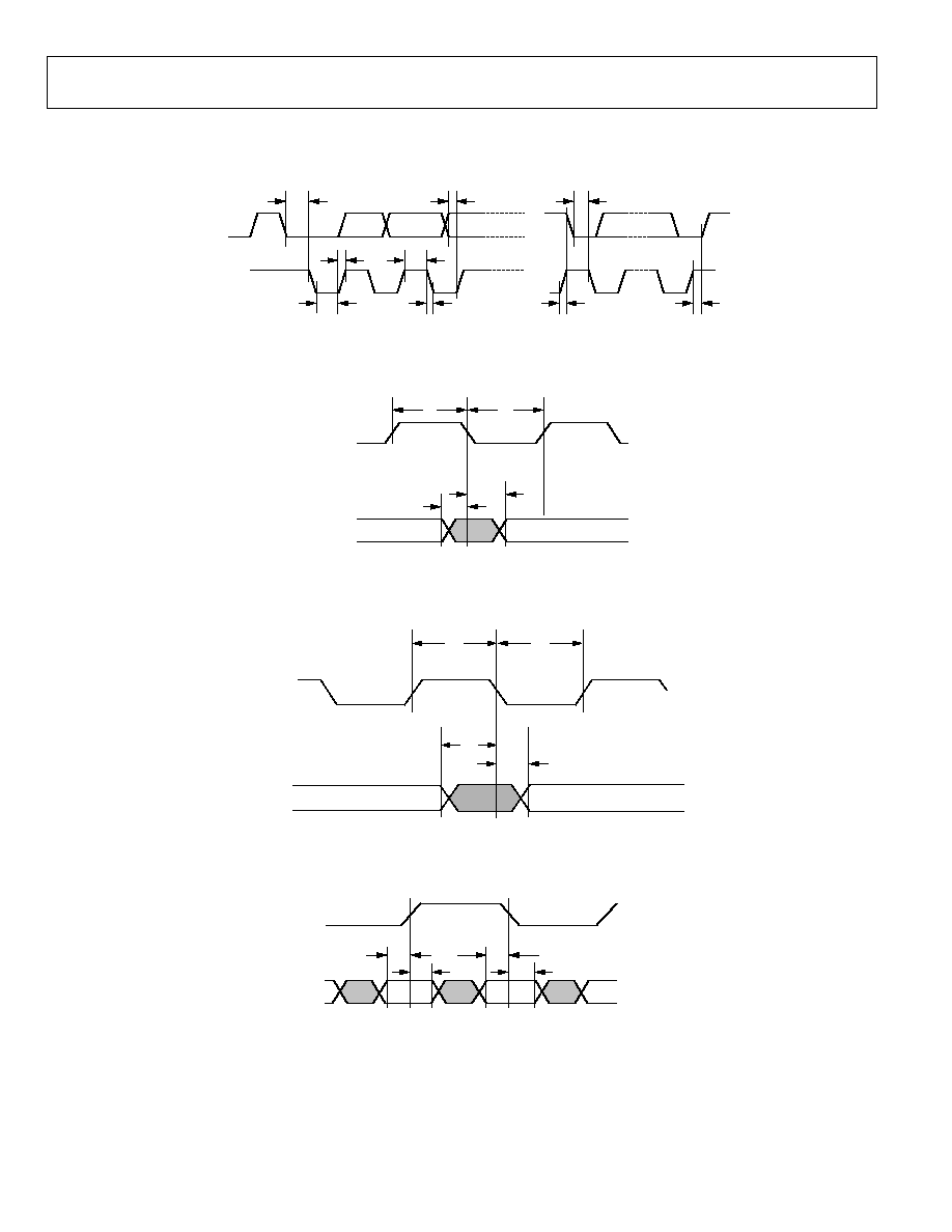
TIMING DIAGRAMS
05000-003
SDA1/SDA2
SCLK1/SCLK2
t
5
t
3
t
4
t
8
t
6
t
7
t
2
t
1
t
3
Figure 3. I
2
C Timing
05000-004
LLC1
P2P9, P12P19,
P22P29, VS, HS,
FIELD/DE,
SFL/SYNC_OUT
t
9
t
10
t
12
t
11
Figure 4. Pixel Port and Control Output SDR Timing (SD Core)
05000-005
t
9
LLC1
P2P9, P12P19,
P22P29
t
13
t
14
t
10
Figure 5. Pixel Port SDR Timing (CP Core)
LLC1
P6P9,
P12P19
t
16
t
18
t
15
t
17
05000-006
Figure 6. Pixel Port DDR Timing (CP Core)
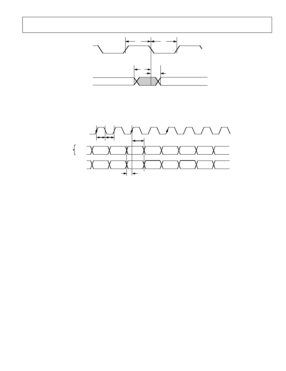
ADV7400A
Rev. A | Page 15 of 16
05000-007
LLC1
VS, HS,
FIELD/DE
t
14
t
9
t
13
t
10
Figure 7. Control Output SDR/DDR Timing (CP Core)
t
9
t
10
t
20
t
19
DCLK_IN
DE_IN
HS_IN
VS_IN
CONTROL
INPUTS
05000-008
P0P1, P10P11,
P20P21, P22P29,
P31P32, P33P40
Figure 8. Digital Input Port and Control Input Timing
ADV7400A
Rev. A | Page 16 of 16
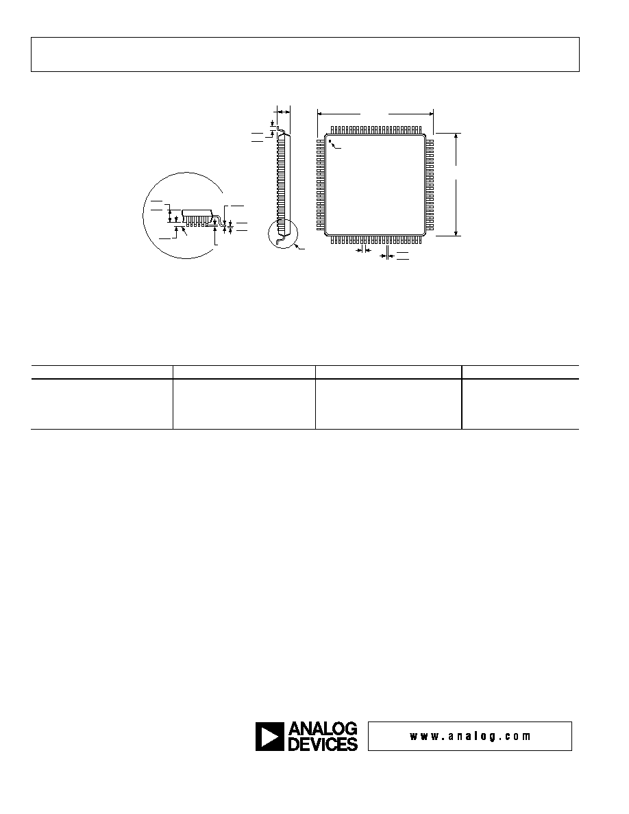
OUTLINE DIMENSIONS
COMPLIANT TO JEDEC STANDARDS MS-026-BED
TOP VIEW
(PINS DOWN)
1
25
26
51
50
75
76
100
0.50
BSC
LEAD PITCH
0.27
0.22
0.17
1.60 MAX
0.75
0.60
0.45
VIEW A
16.00
BSC SQ
14.00
BSC SQ
PIN 1
1.45
1.40
1.35
0.15
0.05
0.20
0.09
0.08 MAX
COPLANARITY
VIEW A
ROTATED 90° CCW
SEATING
PLANE
7°
3.5°
0°
Figure 9. 100-Lead Low Profile Quad Flat Package [LQFP]
(ST-100)
Dimensions shown in millimeters
ORDERING GUIDE
Model
Temperature Range
Package Description
Package Option
ADV7400AKSTZ-110
1
-25°C to +70°C
100-Lead LQFP
ST-100
ADV7400AKSTZ-80
1
-25°C to +70°C
100-Lead LQFP
ST-100
ADV7400ABSTZ-110
1
-40°C to + 85°C
100-Lead LQFP
ST-100
EVAL-ADV7400AEBM
Evaluation
Board
1
Z = Pb-free part. The ADV7400A is a Pb-free environmentally friendly product. It is manufactured using the most up-to-date materials and processes. The coating on
the leads of each device is 100% pure Sn electroplate. The device is suitable for Pb-free applications, and is able to withstand surface-mount soldering at up to 255°C
(±5°C). In addition, it is backward compatible with conventional SnPb soldering processes. This means that the electroplated Sn coating can be soldered with SnPb
solder pastes at conventional reflow temperatures of 220°C to 235°C.
Purchase of licensed I
2
C components of Analog Devices or one of its sublicensed Associated Companies conveys a license for the purchaser under the Philips I
2
C Patent
Rights to use these components in an I
2
C system, provided that the system conforms to the I
2
C Standard Specification as defined by Philips.
© 2005 Analog Devices, Inc. All rights reserved. Trademarks and
registered trademarks are the property of their respective owners.
D0500003/05(A)