 | ÐлекÑÑоннÑй компоненÑ: ADXL105J | СкаÑаÑÑ:  PDF PDF  ZIP ZIP |
ADXL105 DS
REV. A
Information furnished by Analog Devices is believed to be accurate and
reliable. However, no responsibility is assumed by Analog Devices for its
use, nor for any infringements of patents or other rights of third parties
which may result from its use. No license is granted by implication or
otherwise under any patent or patent rights of Analog Devices.
a
ADXL105*
One Technology Way, P.O. Box 9106, Norwood, MA 02062-9106, U.S.A.
Tel: 781/329-4700
World Wide Web Site: http://www.analog.com
Fax: 781/326-8703
© Analog Devices, Inc., 1999
i
MEM
S
is a registered trademark of Analog Devices, Inc.
*Patent Pending.
FEATURES
Monolithic IC Chip
2 m
g Resolution
10 kHz Bandwidth
Flat Amplitude Response ( 1%) to 5 kHz
Low Bias and Sensitivity Drift
Low Power 2 mA
Output Ratiometric to Supply
User Scalable
g Range
On-Board Temperature Sensor
Uncommitted Amplifier
Surface Mount Package
+2.7 V to +5.25 V Single Supply Operation
1000
g Shock Survival
APPLICATIONS
Automotive
Accurate Tilt Sensing with Fast Response
Machine Health and Vibration Measurement
Affordable Inertial Sensing of Velocity and Position
Seismic Sensing
Rotational Acceleration
GENERAL DESCRIPTION
The ADXL105 is a high performance, high accuracy and com-
plete single-axis acceleration measurement system on a single
monolithic IC. The ADXL105 offers significantly increased
bandwidth and reduced noise versus previously available micro-
machined devices. The ADXL105 measures acceleration with a
full-scale range up to
±
5 g and produces an analog voltage out-
put. Typical noise floor is 225
µ
g
Hz allowing signals below
2 mg to be resolved. A 10 kHz wide frequency response enables
vibration measurement applications. The product exhibits signifi-
cant reduction in offset and sensitivity drift over temperature
compared to the ADXL05.
The ADXL105 can measure both dynamic accelerations, (typi-
cal of vibration) or static accelerations (such as inertial force,
gravity or tilt).
Output scale factors from 250 mV/g to 1.5 V/g are set using the
on-board uncommitted amplifier and external resistors. The
device features an on-board temperature sensor with an output
of 8 mV/
°
C for optional temperature compensation of offset vs.
temperature for high accuracy application.
The ADXL105 is available in a hermetic 14-lead surface mount
Cerpak with versions specified for the 0
°
C to +70
°
C, and
40
°
C to +85
°
C temperature ranges.
High Accuracy 1
g to 5 g Single Axis
i
MEM
S
®
Accelerometer with Analog Input
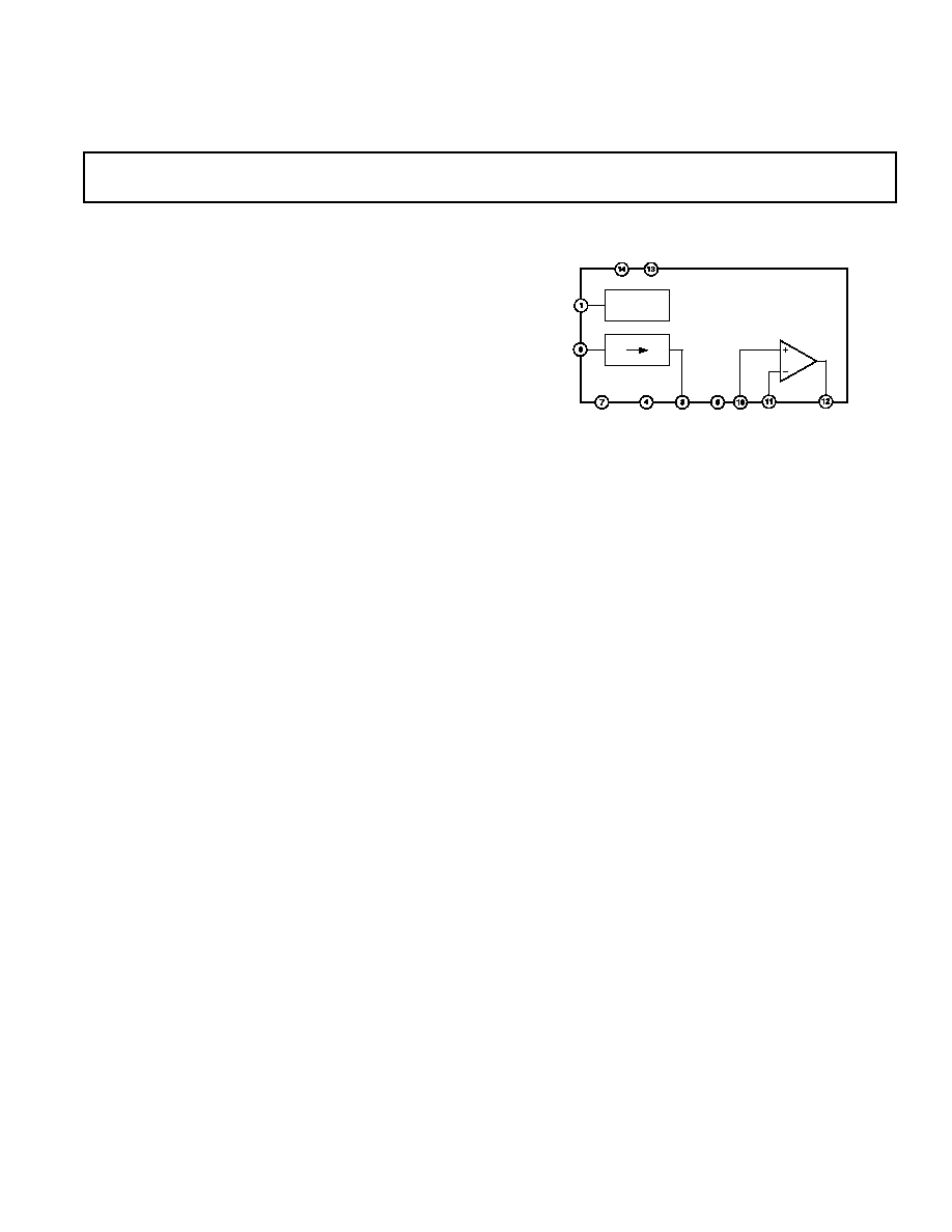
FUNCTIONAL BLOCK DIAGRAM
V
DD
T
OUT
ST
COM
A
OUT
V
MID
V
IN
V
NIN
UCA
OUT
UNCOMMITTED
AMPLIFIER
ADXL105
X SENSOR
TEMP
SENSOR
COM

REV. A
2
ADXL105SPECIFICATIONS
ADXL105J/A
Parameter
Conditions
Min
Typ
Max
Units
SENSOR INPUT
Measurement Range
1
±
5
±
7
g
Nonlinearity
Best Fit Straight Line
0.2
% of FS
Alignment Error
2
±
1
Degrees
Cross Axis Sensitivity
3
Z Axis, @ +25
°
C
±
1
±
5
%
SENSITIVITY
4
(Ratiometric)
At A
OUT
Initial
225
250
275
mV/g
V
S
= 2.7 V
80
105
120
mV/g
vs. Temperature
5, 6
±
0.5
%
ZERO g BIAS LEVEL
5
(Ratiometric)
At A
OUT
Zero g Offset Error
From +2.5 V Nominal
625
+625
mV
vs. Supply
20
+20
mV/V
DD
/V
vs. Temperature
5, 7
50
mV
NOISE PERFORMANCE
Voltage Density
7
@ +25
°
C
225
325
µ
g/
Hz
Noise in 100 Hz Bandwidth
2.25
mg rms
FREQUENCY RESPONSE
3 dB Bandwidth
10
12
kHz
Sensor Resonant Frequency
13
18
kHz
TEMP SENSOR
4
(Ratiometric)
Output Error at +25
°
C
From +2.5 V Nominal
100
+100
mV
Nominal Scale Factor
8
mV/
°
C
Output Impedance
10
k
V
MID
4
(Ratiometric)
Output Error
From +2.5 V Nominal
15
+15
mV
Output Impedance
10
k
SELF-TEST
(Proportional to V
DD
)
Voltage Delta at A
OUT
Self-Test "0" to "1"
100
500
mV
Input Impedance
8
30
50
k
A
OUT
Output Drive
I =
±
50
µ
A
0.50
V
S
0.5
V
Capacitive Load Drive
1000
pF
UNCOMMITTED AMPLIFIER
Initial Offset
25
+25
mV
Initial Offset vs. Temperature
5
µ
V/
°
C
Common-Mode Range
1.0
4.0
V
Input Bias Current
9
25
nA
Open Loop Gain
100
V/mV
Output Drive
I =
±
100
µ
A
0.25
V
S
0.25
V
Capacitive Load Drive
1000
pF
POWER SUPPLY
Operating Voltage Range
2.70
5.25
V
Quiescent Supply Current
At 5.0 V
1.9
2.6
mA
At 2.7 V
1.3
2.0
mA
Turn-On Time
700
µ
s
TEMPERATURE RANGE
Operating Range J
0
+70
°
C
Specified Performance A
40
+85
°
C
NOTES
1
Guaranteed by tests of zero g bias, sensitivity and output swing.
2
Alignment of the X axis is with respect to the long edge of the bottom half of the Cerpak package.
3
Cross axis sensitivity is measured with an applied acceleration in the Z axis of the device.
4
This parameter is ratiometric to the supply voltage V
DD
. Specification is shown with a 5.0 V V
DD
. To calculate approximate values at another V
DD
, multiply the specification by
V
DD
/5 V.
5
Specification refers to the maximum change in parameter from its initial value at +25
°
C to its worst case value at T
MIN
to T
MAX
.
6
See Figure 3.
7
See Figure 2.
8
CMOS and TTL Compatible.
9
UCA input bias current is tested at final test.
All min and max specifications are guaranteed. Typical specifications are not tested or guaranteed.
Specifications subject to change without notice.
(T
A
= T
MIN
to T
MAX
, T
A
= +25 C for J Grade Only, V
S
= +5 V, @ Acceleration = 0
g,
unless otherwise noted)
REV. A
3
ADXL105
ABSOLUTE MAXIMUM RATINGS*
Acceleration (Any Axis, Unpowered for 0.5 ms) . . . . . .1000 g
Acceleration (Any Axis, Powered for 0.5 ms) . . . . . . . . . 500 g
+V
S
. . . . . . . . . . . . . . . . . . . . . . . . . . . . . . . . 0.3 V to +7.0 V
Output Short Circuit Duration
(Any Pin to Common) . . . . . . . . . . . . . . . . . . . . Indefinite
Operating Temperature . . . . . . . . . . . . . . . . 55
°
C to +125
°
C
Storage Temperature . . . . . . . . . . . . . . . . . . 65
°
C to +150
°
C
*Stresses above those listed under Absolute Maximum Ratings may cause perma-
nent damage to the device. This is a stress rating only; the functional operation of
the device at these or any other conditions above those indicated in the operational
sections of this specification is not implied. Exposure to absolute maximum rating
conditions for extended periods may affect device reliability.
Package Characteristics
Package
JA
JC
Device Weight
14-Lead Cerpak
110
°
C/W
30
°
C/W
<2 Grams
ORDERING GUIDE
Model
Temperature Range
Package Option
ADXL105JQC
0
°
C to +70
°
C
QC-14
ADXL105AQC
40
°
C to +85
°
C
QC-14
PIN FUNCTION DESCRIPTIONS
Pin No.
Name
Description
1
T
OUT
Temperature Sensor Output
2, 3, 5
NC
No Connect
4
COM
Common
6
ST
Self-Test
7
COM
Common (Substrate)
8
A
OUT
Accelerometer Output
9
V
MID
V
DD
/2 Reference Voltage
10
V
NIN
Uncommitted Amp Noninverting Input
11
V
IN
Uncommitted Amp Inverting Input
12
UCA
OUT
Uncommitted Amp Output
13, 14
V
DD
Power Supply Voltage
PIN CONFIGURATION
CAUTION
ESD (electrostatic discharge) sensitive device. Electrostatic charges as high as 4000 V readily
accumulate on the human body and test equipment and can discharge without detection.
Although the ADXL105 features proprietary ESD protection circuitry, permanent damage may
occur on devices subjected to high energy electrostatic discharges. Therefore, proper ESD
precautions are recommended to avoid performance degradation or loss of functionality.
WARNING!
ESD SENSITIVE DEVICE
Drops onto hard surfaces can cause shocks of greater than 1000 g
and exceed the absolute maximum rating of the device. Care should
be exercised in handling to avoid damage.
14
13
12
11
10
9
8
1
2
3
4
5
6
7
14
13
12
11
10
9
8
1
2
3
4
5
6
7
14
13
12
11
10
9
8
1
2
3
4
5
6
7
A
OUT
= 2.75V
A
OUT
= 2.50V
A
OUT
= 2.25V
Figure 1. ADXL105 Response Due to Gravity
TOP VIEW
(Not to Scale)
14
13
12
11
10
9
8
1
2
3
4
5
6
7
NC = NO CONNECT
NC
NC
COM
NC
ST
COM
V
DD
UCA
OUT
V
IN
V
NIN
V
MID
A
OUT
T
OUT
ADXL105
V
DD
REV. A
ADXL105
4
Typical Performance Characteristics
TEMPERATURE C
120
120
50
100
0
g
OFFSET SHIFT mV
0
50
30
0
90
60
30
60
90
Figure 2. Typical 0 g Shift vs. Temperature*
TEMPERATURE C
5
2
50
100
SENSITIVITY CHANGE %
0
50
2
1
4
3
0
1
Figure 3. Typical Sensitivity Shift vs. Temperature*
OUTPUT V
20
6
0
2.2 2.25
% OF UNITS
2.3 2.35 2.4 2.45 2.5 2.55 2.6 2.65 2.7 2.75 2.8
18
8
4
2
14
10
16
12
Figure 4. 0 g Output Distribution*
SENSITIVITY V/
g
25
0
0.242
0.260
0.244
% OF UNITS
0.246 0.248 0.250 0.252 0.254
0.258
10
5
20
15
0.256
Figure 5. Sensitivity Distribution*
SUPPLY VOLTAGE
2.5
0
2.7
5.5
CURRENT mA
3.3
4
1
0.5
2
1.5
5
Figure 6. Typical Supply Current vs. Supply Voltage
FREQUENCY Hz
6
18
100
100000
OUTPUT dB
12
10000
1000
12
0
6
18
Figure 7. Noise Graph
*Data from several characterization lots.
REV. A
5
ADXL105
SUPPLY VOLTAGE
500
2
6
NOISE
g
/
Hz
3
4
5
450
400
350
300
250
200
150
Figure 8. Typical Noise Density vs. Supply Voltage
NOISE DENSITY
g
/
Hz
40
0
205
250
210
% OF UNITS
215
220
225
230
235
245
25
20
35
30
240
15
10
5
Figure 9. Noise Distribution*
DEGREES OF MISALIGNMENT
20
0
1.375
0.625
% OF PARTS
0.375
0.0125
0.0125
0.375
0.625
1.125
14
12
18
16
0.875
10
8
6
0.875
1.125
1.375
4
2
Figure 10. Rotational Die Alignment*
Figure 11. Typical Self-Test Response at V
DD
= 5 V
FREQUENCY Hz
1
10000
OUTPUT dB
10
100
1000
15
10
5
0
5
10
15
100000
ADXL105 SOLDERED AND GLUED TO PCB
ADXL105 SOLDERED TO PCB
Figure 12. Frequency Response
FREQUENCY Hz
1
10000
PHASE Degrees
10
100
1000
400
300
200
100
0
100
200
100000
ADXL105 SOLDERED AND GLUED TO PCB
ADXL105 SOLDERED TO PCB
300
Figure 13. Phase Response
*Data from several characterization lots.
REV. A
ADXL105
6
THEORY OF OPERATION
The ADXL105 is a complete acceleration measurement system
on a single monolithic IC. It contains a polysilicon surface-
micromachined sensor and BiMOS signal conditioning circuitry
to implement an open loop acceleration measurement architec-
ture. The ADXL105 is capable of measuring both positive and
negative accelerations to a maximum level of
±
5 g. The acceler-
ometer also measures static acceleration such as gravity, allow-
ing it to be used as a tilt sensor.
The sensor is a surface micromachined polysilicon structure
built on top of the silicon wafer. Polysilicon springs suspend the
structure over the surface of the wafer and provide a resistance
against acceleration-induced forces. Deflection of the structure
is measured with a differential capacitor structure that consists
of two independent fixed plates and a central plate attached to
the moving mass. A 180
°
out-of-phase square wave drives the
fixed plates. An acceleration causing the beam to deflect, will
unbalance the differential capacitor resulting in an output square
wave whose amplitude is proportional to acceleration. Phase sensi-
tive demodulation techniques are then used to rectify the signal
and determine the direction of the acceleration.
An uncommitted amplifier is supplied for setting the output
scale factor, filtering and other analog signal processing.
A ratiometric voltage output temperature sensor measures the
exact die temperature and can be used for optional calibration
of the accelerometer over temperature.
V
DD
The ADXL105 has two power supply (V
DD
) pins, 13 and 14.
The two pins should be connected directly together. The output
of the ADXL105 is ratiometric to the power supply. Therefore a
0.22
µ
F decoupling capacitor between V
DD
and COM is re-
quired to reduce power supply noise. To further reduce noise,
insert a resistor (and/or a ferrite bead) in series with the V
DD
pin. See the EMC and Electrical Noise section for more details.
COM
The ADXL105 has two common (COM) pins, 4 and 7. These
two pins should be connected directly together and Pin 7
grounded.
ST
The ST pin (Pin 6) controls the self-test feature. When this pin
is set to V
DD
, an electrostatic force is exerted on the beam of the
accelerometer causing the beam to move. The change in output
resulting from movement of the beam allows the user to test for
mechanical and electrical functionality. This pin may be left
open-circuit or connected to common in normal use. The self-
test input is CMOS and TTL compatible.
A
OUT
The accelerometer output (Pin 8) is set to a nominal scale fac-
tor of 250 mV/g (for V
DD
= 5 V). Note that A
OUT
is guaranteed
to source/sink a minimum of 50
µ
A (approximately 50 k
out-
put impedance). So a buffer may be required between A
OUT
and
some A-to-D converter inputs.
V
MID
V
MID
is nominally V
DD
/2. It is primarily intended for use as a
reference output for the on board uncommitted amplifier (UCA)
as shown in Figures 14a and 14b. Its output impedance is ap-
proximately 10 k
.
V
DD
T
OUT
ST
COM
A
OUT
V
MID
V
IN
V
NIN
UCA
OUT
UNCOMMITTED
AMPLIFIER
ADXL105
X SENSOR
TEMP
SENSOR
OUTPUT
V
DD
R1
R2
+V
COM
0.22 F
GAIN
1
2
3
4
250
500
750
1000
50k
50k
50k
50k
50k
100k
150k
200k
SCALE mV/
g
R1
R2
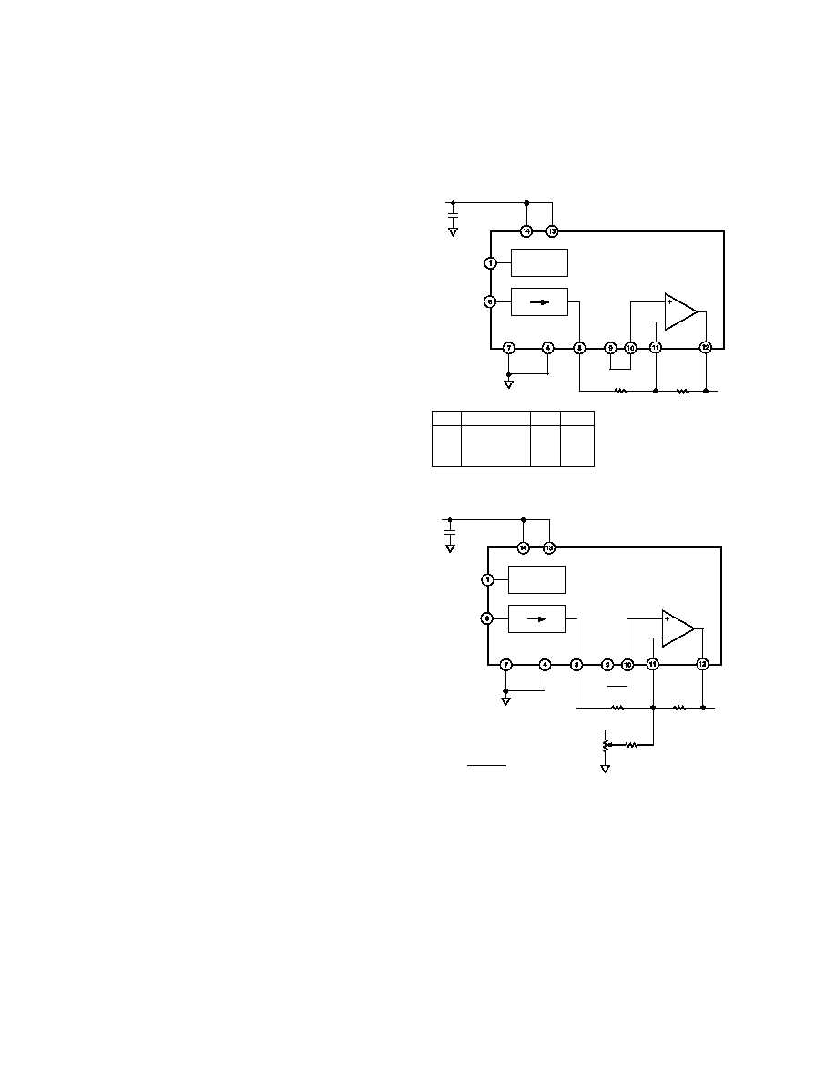
a. Using the UCA to Change the Scale Factor
V
DD
T
OUT
ST
COM
A
OUT
V
MID
V
IN
V
NIN
UCA
OUT
UNCOMMITTED
AMPLIFIER
ADXL105
X SENSOR
TEMP
SENSOR
OUTPUT
V
DD
R1
R2
+V
COM
0.22 F
+V
10k
R3
R3 = 5R1
R1 > 20k
SCALE =
(250) R2
R1
mV/
g
b. Using the UCA to Change the Scale Factor
and Zero g Bias
Figure 14. Application Circuit for Increasing Scale Factor
T
OUT
The temperature sensor output is nominally 2.5 V at +25
°
C and
typically changes 8 mV/
°
C, and is optimized for repeatability
rather than accuracy. The output is ratiometric with supply
voltage.
Uncommitted Amplifier (UCA)
The uncommitted amplifier has a low noise, low drift bipolar
front end design. The UCA can be used to change the scale
factor of the ADXL105 as shown in Figure 14. The UCA may
also be used to add a 1- or 2-pole active filter as shown in Fig-
ures 15a through 15d.
REV. A
7
ADXL105
Output Scaling
The acceleration output (A
OUT
) of the ADXL105 is nominally
250 mV/g. This scale factor may not be appropriate for all appli-
cations. The UCA may be used to increase the scale factor. The
simplest implementation would be as shown in Figure 14a.
Since the 0 g offset of the ADXL105 is 2.5 V
±
625 mV, using a
gain of greater than 4 could result in having the UCA output at
0 V or 5 V at 0 g. The solution is to add R3 and VR1, as shown
in Figure 14b, turning the UCA into a summing amplifier. VR1
is adjusted such that the UCA output is V
DD
/2 at 0 g.
C
R1
OUT
R2
IN
f
3dB
=
1
2 CR1
GAIN =
R1
R2
V
MID
a. 1-Pole Low-Pass Filter
0.22 F
OUT
20k
IN
f
3dB
= 30Hz
20k
0.18 F
V
MID
b. 2-Pole Bessel Low-Pass Filter
R1
OUT
R2
IN
f
3dB
=
1
2 CR2
GAIN =
R1
R2
C
R3
R3 2.5 R1
~
~
V
MID
V
MID
c. 1-Pole High-Pass Filter
44.2k
OUT
IN
f
3dB
= 10Hz
59k
0.39 F
0.39 F
V
MID
d. 2-Pole Bessel High-Pass Filter
Figure 15. UCA Used as Active Filters*
Device Bandwidth vs. Resolution
In general the bandwidth selected will determine the noise floor
and hence, the measurement resolution (smallest detectable
acceleration) of the ADXL105. Since the noise of the ADXL105
has the characteristic of white Gaussian noise that contributes
equally at all frequencies, the noise amplitude may be reduced
by simply reducing the bandwidth. So the typical noise of the
ADXL105 is:
Noise (rms) = (225
µ
g/
Hz)
× (
Bandwidth
×
K)
Where
K
1.6 for a single-pole filter
K
1.4 for a 2-pole filter
So given a bandwidth of 1000 Hz, the typical rms noise floor of
an ADLX105 will be:
Noise = (225
µ
g/
Hz)
×
(
1000
×
1.6)
= 9 mg rms for a single-pole filter
and
Noise = (225
µ
g/
Hz)
×
(
1000
×
1.4)
= 8.4 mg rms for 2-pole filter
Often the peak value of the noise is desired. Peak-to-peak noise
can only be estimated by statistical means. Table I may be used
for estimating the probabilities of exceeding various peak values
given the rms value. The peak-to-peak noise value will give the
best estimate of the uncertainty in a single measurement.
Table I. Estimation of Peak-to-Peak Noise
Nominal Peak-to-
% of Time that Noise Will
Peak Value
Exceed Peak-to-Peak Value
2
×
rms
32%
3
×
rms
13%
4
×
rms
4.6%
5
×
rms
1.2%
6
×
rms
0.27%
7
×
rms
0.047%
8
×
rms
0.0063%
The UCA may be configured to act as an active filter with gain
and 0 g offset control as shown in Figure 16.
0.1 F
OUT
IN
GAIN = 2
f
3dB
= 30Hz
0.1 F
100k
47k
47k
10k
V
DD
47k
Figure 16. UCA Configured as an Active Low-Pass Filter
with Gain and Offset
EMC and Electrical Noise
The design of the ADXL105 is such that EMI or magnetic
fields do not normally affect it. Since the ADXL105 is ratiomet-
ric, conducted electrical noise on V
DD
does affect the output.
This is particularly true for noise at the ADXL105's internal
clock frequency (200 kHz) and its odd harmonics. So maintain-
ing a clean supply voltage is key in preserving the low noise and
high resolution properties of the ADXL105.
One way to ensure that V
DD
contains no high frequency noise is
to add an R-C low-pass filter near the V
DD
pin as shown in
Figure 17. Using the component values shown in Figure 17,
noise at 200 kHz is attenuated by approximately 23 dB. As-
suming the ADXL105 consumes 2 mA, there will be a 100 mV
drop across R1. This can be neglected simply by using the
ADXL105's V
DD
as the A-to-D converter's reference voltage as
shown in Figure 17.
*For other corner frequencies, consult an active filter handbook.
REV. A
ADXL105
8
C3549a19/99
PRINTED IN U.S.A.
Dynamic Operation
In applications where only dynamic accelerations (vibration) are
of interest, it is often best to ac-couple the accelerometer output
as shown in Figures 15c and 15d. The advantage of ac coupling
is that 0g offset variability (part to part) and drifts are eliminated.
Low Power Operation
The most straightforward method of lowering the ADXL105's
power consumption is to minimize its supply voltage. By lower-
ing V
DD
from 5 V to 2.7 V the power consumption goes from
9.5 mW to 3.5 mW. There may be reasons why lowering the
supply voltage is impractical in many applications, in which case
the best way to minimize power consumption is by power cycling.
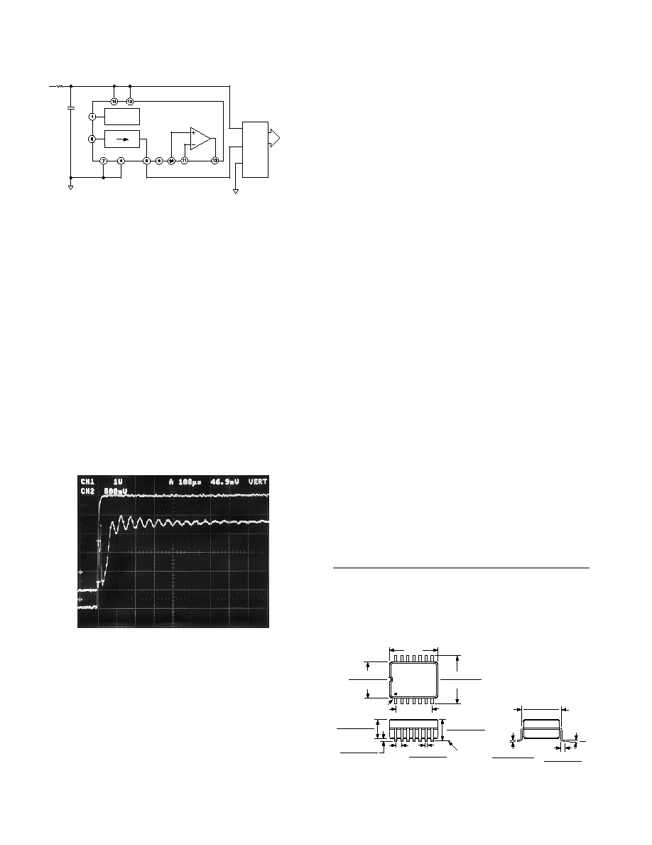
The ADXL105 is capable of turning on and giving an accurate
reading within 700
µ
s (see Figure 18). Most microcontrollers
can perform an A-to-D conversion in under 25
µ
s. So it is prac-
tical to turn on the ADXL105 and take a reading in under 750
µ
s. Given a 100 Hz sample rate the average current required at
2.7 V would be:
100 samples/s
×
750
µ
s
×
1.3 mA = 97.5
µ
A
Figure 18. Typical Turn-On Response at V
DD
= 5 V
Note that if a filter is used in the UCA, sufficient time must be
allowed for the settling of the filter as well.
Broadband Operation
The ADXL105 has a number of characteristics that permits
operation over a wide frequency range. Its frequency and phase
response is essentially flat from dc to 10 kHz (see Figures 12
and 13). Its sensitivity is also constant over temperature (see
Figure 3). In contrast, most accelerometers do not have linear
response at low frequencies (in many cases, no response at very
low frequencies or dc), and often have a large sensitivity tem-
perature coefficient that must be compensated for. In addi-
tion, the ADXL105's noise floor is essentially flat from dc to
5 kHz where it gently rolls off (see Figure 7). The beam reso-
nance at 16 kHz can be seen in Figure 7 where there is a small
noise peak (+5 dB) at the beam's resonant frequency. There are
no other significant noise peaks at any frequency.
The resonant frequency of the beam in the ADXL105 deter-
mines its high frequency limit. However the resonant frequency
of the Cerpak package is typically around 7 kHz. As a result, it
is not unusual to see 6 dB peaks occurring at the package reso-
nant frequency (as shown in Figures 12 and 13). Indeed, the
PCB will often have one or more resonant peaks well below
7 kHz. Therefore, if the application calls for accurate operation
at or above 6 kHz the ADXL105 should be glued to the PCB in
order to eliminate the amplitude response peak due to the pack-
age, and careful consideration should be given to the PCB
mechanical design.
CALIBRATING THE ADXL105
The initial value of the offset and scale factor for the ADXL105
will require dc calibration for applications such as tilt
measurement.
For low g applications, the force of gravity is the most stable,
accurate and convenient acceleration reference available. An
approximate reading of the 0 g point can be determined by
orienting the device parallel to the Earth's surface and then
reading the output. For high accuracy, a calibrated fixture must
be used to ensure exact 90 degree orientation to the 1 g gravity
signal.
An accurate sensitivity calibration method is to make a measure-
ment at +1 g and 1 g. The sensitivity can be determined by the
two measurements. This method has the advantage of being less
sensitive to the alignment of the accelerometer because the on
axis signal is proportional to the Cosine of the angle. For ex-
ample, a 5
°
error in the orientation results in only a 0.4% error
in the measurement.
To calibrate, the accelerometer measurement axis is pointed
directly at the Earth. The 1 g reading is saved and the sensor is
turned 180
°
to measure 1 g. Using the two readings and sensi-
tivity is calculated:
Sensitivity = [1 g Reading (1 g Reading)]/2 V/g
V
DD
T
OUT
ST
COM
A
OUT
V
MID
V
IN
V
NIN
UCA
OUT
UNCOMMITTED
AMPLIFIER
ADXL105
X SENSOR
TEMP
SENSOR
V
DD
0.22 F
50
COM
+V
A-TO-D
CONVERTER
DOUT
VREF
AIN
COM
Figure 17. Reducing Noise on V
DD
OUTLINE DIMENSIONS
Dimensions shown in inches and (mm).
14-Lead Cerpak
(QC-14)
1
7
8
14
0.310 (7.874)
0.275 (6.985)
0.415 (10.541)
MAX
PIN 1
0.300 (7.62)
0.419 (10.643)
0.394 (10.008)
0.345 (8.763)
0.290 (7.366)
0.050 (1.270)
0.016 (0.406)
8
0
0.0125 (0.318)
0.009 (0.229)
SEATING
PLANE
0.170 (4.318)
0.135 (3.429)
0.190 (4.826)
0.140 (3.556)
0.020 (0.508)
0.013 (0.330)
0.050
(1.27)
BSC
0.020 (0.508)
0.004 (0.102)