Äîêóìåíòàöèÿ è îïèñàíèÿ www.docs.chipfind.ru
REV. 0
Information furnished by Analog Devices is believed to be accurate and
reliable. However, no responsibility is assumed by Analog Devices for its
use, nor for any infringements of patents or other rights of third parties
which may result from its use. No license is granted by implication or
otherwise under any patent or patent rights of Analog Devices.
a
ADXL190*
One Technology Way, P.O. Box 9106, Norwood, MA 02062-9106, U.S.A.
Tel: 781/329-4700
World Wide Web Site: http://www.analog.com
Fax: 781/326-8703
© Analog Devices, Inc., 1999
Low Cost 100
g Single Axis
Accelerometer with Analog Output
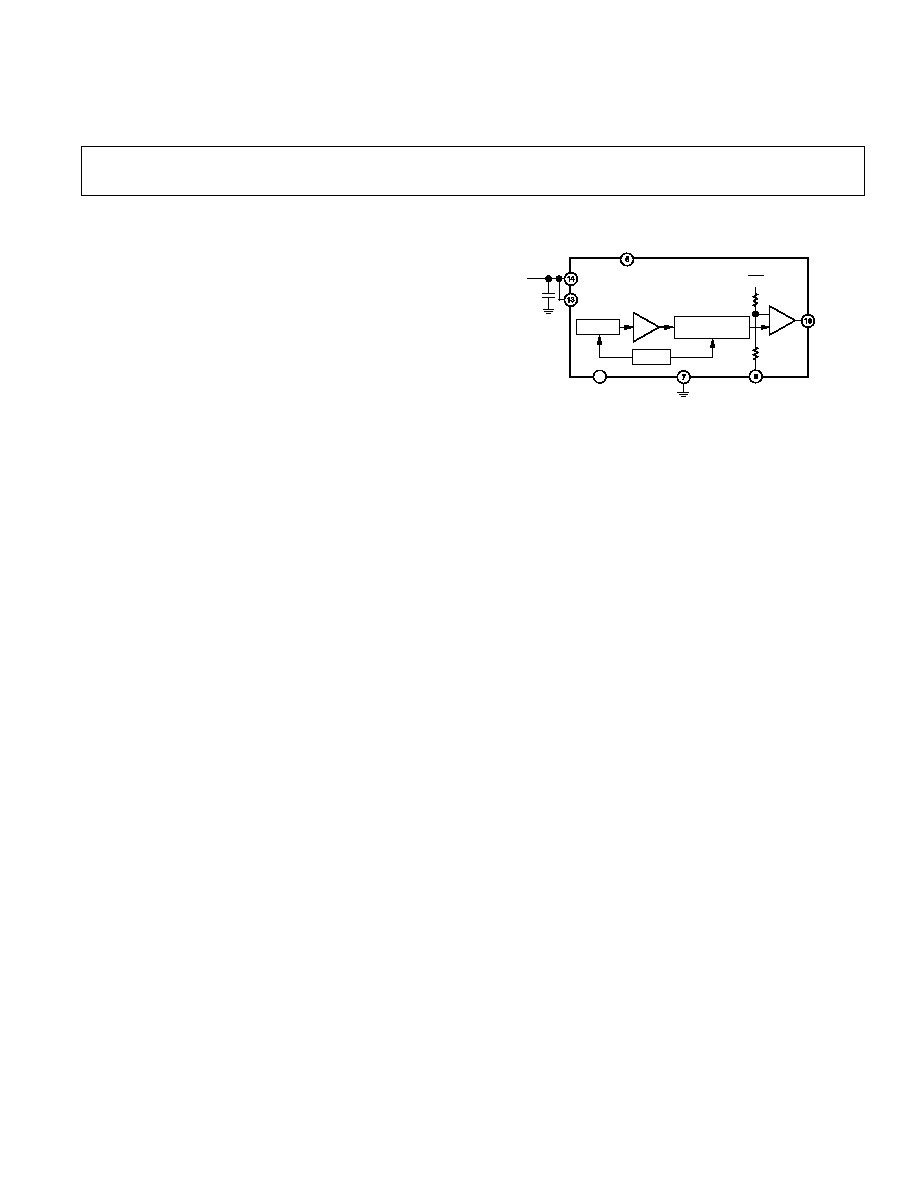
FUNCTIONAL BLOCK DIAGRAM
SELF-TEST
+V
S
2
25k
5k
ADXL190
GAIN
AMP
ZERO
g
ADJUST
COM
0.1 F
BUFFER
AMP
DEMODULATOR
SENSOR
+V
S
TP
(DO NOT CONNECT)
V
OUT
9
CLOCK
i
MEM
S
is a registered trademark of Analog Devices, Inc.
*Patent Pending.
FEATURES
i
MEM
S
®
Single Chip IC Accelerometer
40 Milli-
g Resolution
Low Power 2 mA
400 Hz Bandwidth
+5.0 V Single Supply Operation
2000
g Shock Survival
APPLICATIONS
Shock and Vibration Measurement
Machine Health
Shipping Recorders
Military Fuze, Safe and Arm
GENERAL DESCRIPTION
The ADXL190 is a complete acceleration measurement system
on a single monolithic IC. It contains a polysilicon surface-
micromachined sensor and signal conditioning circuitry to
implement an open-loop acceleration measurement architecture.
The ADXL190 is capable of measuring both positive and nega-
tive accelerations up to
±
100 g, making it suitable for shock and
vibration measurement.
Typical noise floor is 4 mg/
Hz allowing signals below 40 milli-g
to be resolved. The ADXL190 can measure both dynamic accel-
erations, (typical of vibration) or static accelerations, (such as
inertial force or gravity).
The ADXL190 has a two-pole Bessel switched-capacitor filter.
Bessel filters, sometimes called linear phase filters, have a step
response with minimal overshoot and a maximally flat group
delay. The 3 dB frequency of the poles is preset at the factory
to 400 Hz. These filters are also completely self-contained and
buffered, requiring no external components.
The product features a built-in self-test feature that exercises
both the mechanical structure and electrical circuitry. When
triggered by a logic high on the self-test pin, an electrostatic
force acts on the beam equivalent to approximately 20% of full-
scale acceleration input, and thus a proportional voltage change
appears on the output pin. No external components other than a
decoupling capacitor are required.
The ADXL190 is available in a hermetic 14-lead surface mount
cerpak, specified over the 40
°
C to +105
°
C temperature range.

REV. 0
2
ADXL190SPECIFICATIONS
ADXL190WQC
Parameter
Conditions
Min
Typ
Max
Units
SENSOR INPUT
Dynamic Range
1, 2, 3
Without Zero-g Adjust
±
105
g
Alignment Error
±
1
Degrees
Nonlinearity
0.2
%
Cross Axis Sensitivity
±
2
%
SENSITIVITY
Initial
4
Ratiometric
16.5
18.0
19.5
mV/g
Temperature Drift
5
from +25
°
C
±
0.5
%
ZERO g BIAS LEVEL
Initial
2, 3
Ratiometric
2.3
2.5
2.7
V
0 g Offset vs. Temperature
5
from +25
°
C
1.0
g
Zero g Adjustment Gain
0.45
0.50
0.55
V
OUT
/
V 0 g Adjust
Zero g Adjust Pin Input Impedance
20
30
40
k
NOISE PERFORMANCE
Noise Density
4
12
mg/
Hz rms
FREQUENCY RESPONSE
3 dB Bandwidth
360
400
Hz
Sensor Resonant Frequency
24
kHz
SELF-TEST
Output Change
6
450
990
mV
Logic "1" Voltage
3.5
V
Logic "0" Voltage
1.0
V
Input Impedance
50
k
ANALOG OUTPUT
Output Voltage Range
I
OUT
=
±
100
µ
A
0.25
V
S
0.25
V
Capacitive Load Drive
1000
pF
POWER SUPPLY
Specified Performance
4.75
5.25
V
Quiescent Supply Current
2.0
5.0
mA
TEMPERATURE RANGE
Specified Performance
40
+105
°
C
NOTES
1
Product is tested at
±
50 g, and the combination of 0-g error, sensitivity error, and output voltage swing measurements provide the calculations for dynamic range.
2
0-g is nominally V
S
/2. Use of the 0-g adjustment pin is used to null the 0-g error, resulting in increased dynamic range. It can also be used to create an asymmetrical
dynamic range if so desired.
3
The output response is ratiometric and is described by the following equation. V
OUT
(accel, V
S
) = [V
S
/2
±
(a V
S
/5 V)] + [(accel) (b V
S
+ c V
S
2
)(1
±
0.08)]
Where a = 0.2 V, b = 2.712
×
10
3
1/g , c = 0.178
×
10
3
1/g/V.
4
Measured at 100 Hz,
±
50 g.
5
Specification refers to the maximum change in parameter from its initial value at +25
°
C to its worst case value at T
MIN
or T
MAX
.
6
ST pin Logic "0" to "1";
V
OUT
= (
V
OUT
@ 5 V)
×
(V
S
/5 V).
All min and max specifications are guaranteed. Typical specifications are not tested or guaranteed.
Specifications subject to change without notice.
(T
A
= T
MIN
to T
MAX
, V
S
= +5 V, Acceleration = 0
g unless otherwise noted)
REV. 0
ADXL190
3
ABSOLUTE MAXIMUM RATINGS*
Acceleration (Any Axis, Unpowered for 0.5 ms) . . . . . . 2000 g
Acceleration (Any Axis, Powered for 0.5 ms) . . . . . . . . 1000 g
+V
S
. . . . . . . . . . . . . . . . . . . . . . . . . . . . . . . . 0.3 V to +7.0 V
Short Circuit Duration (Any Pin to Common) . . . . Indefinite
Operating Temperature . . . . . . . . . . . . . . . . 55
°
C to +125
°
C
Storage Temperature . . . . . . . . . . . . . . . . . . 65
°
C to +150
°
C
*Stresses above those listed under Absolute Maximum Ratings may cause perma-
nent damage to the device. This is a stress rating only; the functional operation of
the device at these or any other conditions above those indicated in the operational
sections of this specification is not implied. Exposure to absolute maximum rating
conditions for extended periods may affect device reliability.
Drops onto hard surfaces can cause shocks of greater than 2000 g
and exceed the absolute maximum rating of the device. Care
should be exercised in handling to avoid damage.
PIN FUNCTION DESCRIPTIONS
Pin No.
Function
1, 2, 3, 4, 6, 11, 12
No Connect
5
Test Point (Do Not Connect)
7
Common
8
Zero g Adjust
9
Self-Test
10
V
OUT
13, 14
V
S
PACKAGE CHARACTERISTICS
Package
JA
JC
Device Weight
14-Lead Cerpak
+110
°
C/W
+30
°
C/W
5 Grams
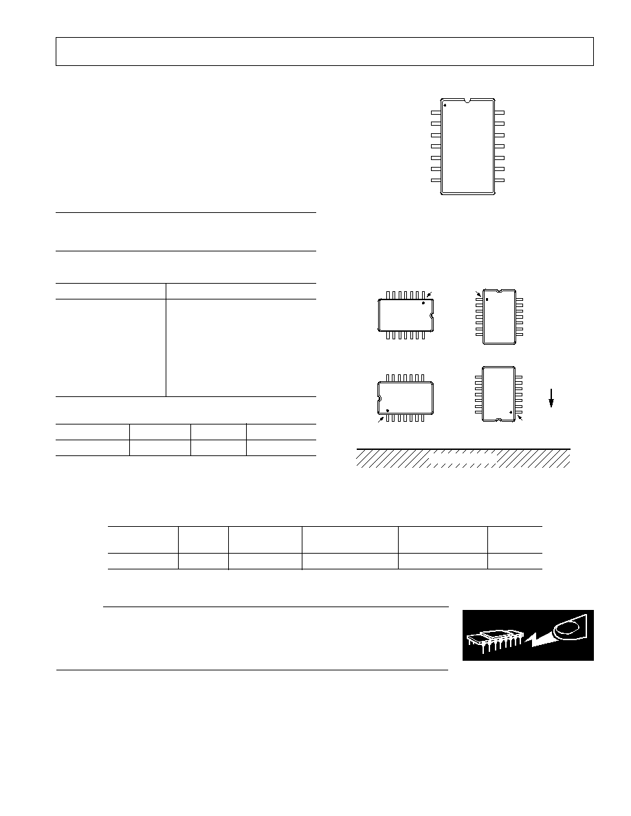
PIN CONFIGURATION
TOP VIEW
(Not to Scale)
14
13
12
11
10
9
8
1
2
3
4
5
6
7
ADXL190
NC
NC
NC
NC
NC
COMMON
V
S
NC
NC
V
OUT
SELF-TEST
ZERO
g
ADJUST
NC = NO CONNECT
V
S
TEST POINT
(DO NOT CONNECT)
Figure 1 shows the response of the ADXL190 to the earth's
gravitational field. The output values shown are nominal. They
are presented to show the user what type of response to expect
from each of the output pins due to changes in orientation with
respect to the earth.
TYPICAL OUTPUT AT
PIN 10 = 2.500V
1
7
8
14
PIN 1
1
g
TYPICAL OUTPUT AT
PIN 10 = 2.482V
1
7
8
14
PIN 1
TYPICAL OUTPUT AT
PIN 10 = 2.500V
1
7
8
14
PIN 1
TYPICAL OUTPUT AT
PIN 10 = 2.518V
1
7
8
14
PIN 1
EARTH'S SURFACE
Figure 1. ADXL190 Response Due to Gravity
CAUTION
ESD (electrostatic discharge) sensitive device. Electrostatic charges as high as 4000 V readily
accumulate on the human body and test equipment and can discharge without detection.
Although the ADXL190 features proprietary ESD protection circuitry, permanent damage may
occur on devices subjected to high energy electrostatic discharges. Therefore, proper ESD
precautions are recommended to avoid performance degradation or loss of functionality.
WARNING!
ESD SENSITIVE DEVICE
ORDERING GUIDE
#
Specified
Temperature
Package
Package
Model
Axis
Voltage
Range
Description
Option
ADXL190WQC
1
+5 V
40
°
C to +105
°
C
14-Lead Cerpak
QC-14
REV. 0
ADXL190
4
APPLICATIONS
All the circuitry needed to drive the sensor and convert the
capacitance change to voltage is incorporated on-chip requiring
no external components except for standard power supply de-
coupling. Both sensitivity and the zero-g value are ratiometric to
the supply voltage, so that ratiometric devices following the
accelerometer (such as an ADC, etc.) will track the accelerom-
eter if the supply voltage changes. The output voltage (V
OUT
) is
a function of both the acceleration input (a) and the power
supply voltage (V
S
) as follows:
V
OUT
= V
S
/2 (Sensitivity
×
V
S
/5 V
×
a)
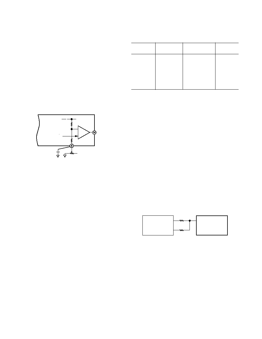
Adjusting the 0 g Bias Level
In some cases the user may have an asymmetrical input or may
want to fine adjust the zero-g output level to obtain maximum
dynamic range. The zero-g level is adjusted by supplying a
voltage to the zero-g adjustment pin (see Figure 2).
+V
S
2
25k
5k
ADXL190
ZERO
g
ADJUST
FILTER
V
OUT
GAIN = 3
ACCELERATION
SIGNAL
+V
S
200k
C2
0.1 F
Figure 2. Optional Zero-g Adjust Circuit Detail
Any voltage difference between the zero-g adjustment pin and
V
S
/2 is reduced by a factor of 6 by the internal resistor divider.
This is then gained by the factor of 3 in the output stage for a
total gain of 0.5 for the zero-g adjustment. (Note: The ratio of
the resistors in the divider is consistent from part-to-part; how-
ever, the absolute values can have a
±
30% tolerance). The
zero-g adjustment voltage can be set up by a variety of methods
including a potentiometer (as shown in Figure 2), a PWM sig-
nal, or with a simple three-state output.
The simplest way is by adding a resistor between the ZERO g
ADJUST pin and V
S
or ground. The output will be offset by:
Offset (V) = (7.5
×
V
S
)/(30 + R)
where R is in k
and connected to V
S
.
Offset (V) = (7.5
×
V
S
)/(30 + R)
where R is in k
and connected to ground.
Resistors may also be connected to microcontroller I/O pins as
shown in Figure 3. Using two I/Os that may be set to V
S
, ground,
or three-state, there are seven possibilities as shown in Table I
(one cannot set one I/O pin to V
S
and the other to ground).
Using such a system, any ADXL190 may be user trimmed to
output 2.5 V
±
35 mV at zero g.
Table I. Offsets Produced Using the Circuit in Figure 3 for V
S
= 5 V
Offset Voltage
P1
P0
Produced
Offset in g
Three-State
Three-State
0 mV
0
Three-State
0
71 mV
4
0
Three-State
134 mV
7.4
0
0
191 mV
10.6
Three-State
1
71 mV
4
1
Three-State
134 mV
7.4
1
1
191 mV
10.6
Another way to adjust the zero g offset is to supply a voltage to
the ZERO g ADJUST pin. The difference between V
S
/2 and
the voltage at the ZERO g ADJUST pin is reduced by a factor
of 6 (as a result of the internal 5 k
and 25 k
voltage divider)
and then multiplied by a factor of 3 in the output stage of the
ADXL190 resulting in a total gain of 0.5. Offset is thus de-
scribed by the following equation:
Offset (V) = (Voltage at the ZERO g ADJUST Pin V
S
/2)/2
This voltage may be produced by a variety of methods includ-
ing a PWM signal from a microcontroller. Care must be taken
that the output impedance of this voltage source is less than
5 k
and that there is very little ripple (noise). Any noise at the
ZERO g ADJUST pin will cause output errors.
If an asymmetric range of acceleration is required (e.g., +75 g
to 125 g) a resistor may be connected between the ZERO g
ADJUST and ground or V
S
as described above. For example:
For a range of +75 g to 125 g the offset required is 25 g.
25 g at 18 mV/g = 450 mV of offset is required.
Rearranging the offset equations above:
R = [(7.5
×
V
S
)/offset] 30 = 53.3 k
connected to ground.
For asymmetric operation the g range midpoint may be shifted
up to
±
80 g typically.
500k
250k
ZERO
g
ADJUST
ADXL190
MICROCONTROLLER
P1
P0
Figure 3. An Offset Adjustment Scheme
REV. 0
ADXL190
5
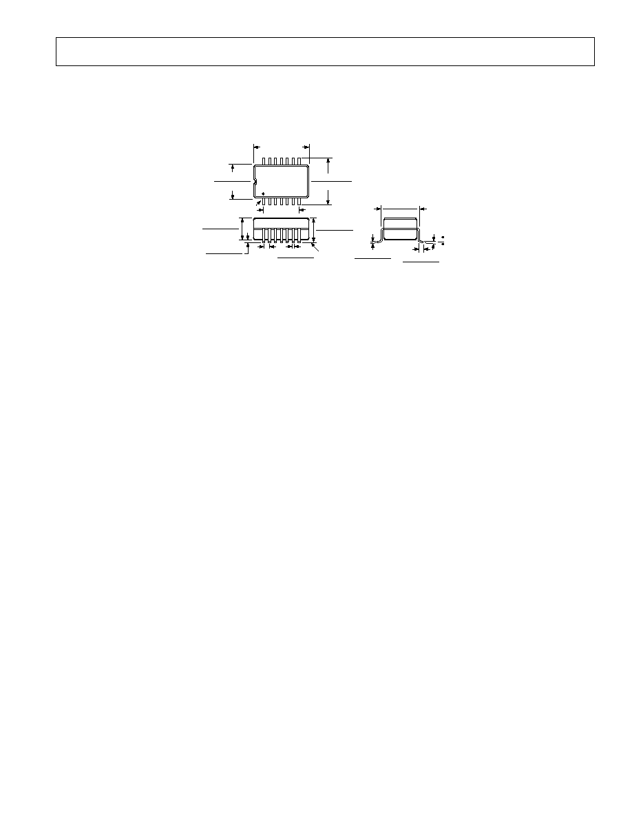
OUTLINE DIMENSIONS
Dimensions shown in inches and (mm).
14-Lead Cerpak
(QC-14)
1
7
8
14
0.291 (7.391)
0.285 (7.239)
0.485 (12.319)
MAX
PIN 1
0.300 (7.62)
0.419 (10.643)
0.394 (10.008)
0.345 (8.763)
0.290 (7.366)
8
0
0.050 (1.270)
0.016 (0.406)
0.013 (0.318)
0.009 (0.229)
SEATING
PLANE
0.195 (4.953)
0.115 (2.921)
0.215 (5.461)
0.119 (3.023)
0.020 (0.508)
0.013 (0.330)
0.050
(1.27)
BSC
0.020 (0.508)
0.004 (0.102)
C345782/99
PRINTED IN U.S.A.