 | –≠–ª–µ–∫—Ç—Ä–æ–Ω–Ω—ã–π –∫–æ–º–ø–æ–Ω–µ–Ω—Ç: ADXL311 | –°–∫–∞—á–∞—Ç—å:  PDF PDF  ZIP ZIP |
Low Cost, Ultracompact
±2
g
Dual-Axis Accelerometer
ADXL311
FEATURES
Low cost
High resolution
Dual-axis accelerometer on a single IC chip
5 mm ◊ 5 mm ◊ 2 mm CLCC package
Low power < 400
µA (typ)
X-axis and Y-axis aligned to within 0.1∞ (typ)
BW adjustment with a single capacitor
Single-supply operation
High shock survival
APPLICATIONS
Tilt and motion sensing in cost-sensitive applications
Smart handheld devices
Computer security
Input devices
Pedometers and activity monitors
Game controllers
Toys and entertainment products
GENERAL DESCRIPTION
The ADXL311 is a low cost, low power, complete dual-axis
accelerometer with signal conditioned voltage outputs, all on a
single monolithic IC. The ADXL311 is built using the same
proven iMEMSÆ process used in over 100 million Analog
Devices accelerometers shipped to date, with demonstrated
1 FIT reliability (1 failure per 1 billion device operating hours).
The ADXL311 will measure acceleration with a full-scale
range of ±2
g. The ADXL311 can measure both dynamic
acceleration (e.g., vibration) and static acceleration (e.g.,
gravity). The outputs are analog voltages proportional to
acceleration.
The typical noise floor is 300 µ
g/
Hz
allowing signals below
2 m
g (0.1∞ of inclination) to be resolved in tilt sensing appli-
cations using narrow bandwidths (10 Hz).
The user selects the bandwidth of the accelerometer using
capacitors C
X
and C
Y
at the X
FILT
and Y
FILT
pins. Bandwidths
of 1 Hz to 2 kHz may be selected to suit the application.
The ADXL311 is available in a 5 mm ◊ 5 mm ◊ 2 mm
8-terminal hermetic CLCC package
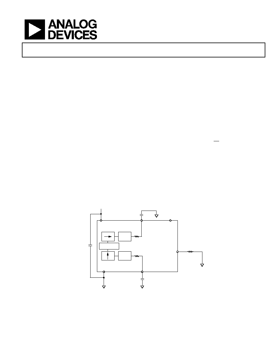
COM
Y
OUT
X
OUT
V
DD
C
X
ADXL311JE
Y SENSOR
3.0V
SELF TEST
X SENSOR
R
FILT
32k
R
FILT
32k
200k
CY
CDC
OSCILLATOR
DEMOD
DEMOD
BIAS
Figure 1. Functional Block Diagram
Rev. A
Information furnished by Analog Devices is believed to be accurate and reliable.
However, no responsibility is assumed by Analog Devices for its use, nor for any
infringements of patents or other rights of third parties that may result from its use.
Specifications subject to change without notice. No license is granted by implication
or otherwise under any patent or patent rights of Analog Devices. Trademarks and
registered trademarks are the property of their respective companies.
One Technology Way, P.O. Box 9106, Norwood, MA 02062-9106, U.S.A.
Tel: 781.329.4700
www.analog.com
Fax: 781.326.8703
© 2003 Analog Devices, Inc. All rights reserved.

ADXL311
TABLE OF CONTENTS
Specifications..................................................................................... 3
Absolute Maximum Ratings............................................................ 4
Typical Performance Characteristics ............................................. 5
Theory of Operation ........................................................................ 7
Applications................................................................................... 7
Design Trade-Offs for Selecting Filter Characteristics: The
Noise/BW Trade-Off.................................................................... 7
Using the ADXL311 as a Dual-Axis Tilt Sensor....................... 8
Pin Configuration and Functional Descriptions...........................9
Outline Dimensions ....................................................................... 10
Ordering Guide .......................................................................... 10
REVISION HISTORY
7/03--Data sheet changed from Rev. 0 to Rev. A.
Change to OUTLINE DIMENSIONS.......................................... 10
Revision 0: Initial Version
Rev. A | Page 2 of 12

ADXL311
Rev. A | Page 3 of 12
SPECIFICATIONS
Table 1. T
A
= 25
o
C, V
DD
= 3 V, R
BIAS
= 125 k, Acceleration = 0
g, unless otherwise noted.)
Parameter Conditions
Min
Typ
Max
Units
SENSOR INPUT
Each Axis
Measurement Range
±2
g
Nonlinearity
Best Fit Straight Line
0.2
% of FS
Aligment Error
1
±1
Degrees
Aligment Error
X Sensor to Y Sensor
0.01
Degrees
Cross Axis Sensitivity
2
±2
%
SENSITIVITY Each
Axis
Sensitivity at X
FILT
, Y
FILT
V
DD
= 3 V
140
167
195
mV/g
Sensitivity Change due to Temperature
3
Delta from 25∞C
-0.025
%/∞C
ZERO g BIAS LEVEL
Each Axis
0 g Voltage X
FILT
, Y
FILT
V
DD
= 3 V
1.2
1.5
1.8
V
0 g Offset vs. Temperature
Delta from 25∞C
2.0
mg/∞C
NOISE PERFORMANCE
Noise Density
@25∞C
300
µg/Hz RMS
FREQUENCY RESPONSE
3 dB Bandwidth
At Pins X
FILT
, Y
FILT
6
kHz
Sensor Resonant Frequency
10
kHz
FILTER
R
FILT
Tolerance
32 k Nominal
±15
%
Minimum Capacitance
At Pins X
FILT
, Y
FILT
1000
pF
SELF TEST
X
FILT
, Y
FILT
Self Test 0 to 1
45
mV
POWER SUPPLY
Operating Voltage Range
2.7
5.25
V
Quiescent Supply Current
0.4
1.0
mA
Turn-On Time
160 ◊ C
FILT
+ 0.3
ms
TEMPERATURE RANGE
Operating Range
0
70
∞C
1
Alignment error is specified as the angle between the true and indicated axis of sensitivity (
).
Figure 1
2
Cross axis sensitivity is the algebraic sum of the alignment and the inherent sensitivity errors.
3
Defined as the output change from ambient to maximum temperature or ambient to minimum temperature.
ADXL311
Rev. A | Page 4 of 12
ABSOLUTE MAXIMUM RATINGS
Table 2.
Parameter Rating
Acceleration
(Any Axis, Unpowered)
3,500 g, 0.5 ms
Acceleration
(Any Axis, Powered, V
DD
= 3 V)
3,500 g, 0.5 ms
V
DD
≠0.3 V to +0.6 V
Output Short-Circuit Duration,
(Any Pin to Commom)
Indefinite
Operating Temperature Range
≠55∞C to +125∞C
Storage Temperature
≠65∞C to +150∞C
Stresses above those listed under Absolute Maximum Ratings
may cause permanent damage to the device. This is a stress rat-
ing only and functional operation of the device at these or any
other conditions above those indicated in the operational sec-
tion of this specification is not implied. Exposure to absolute
maximum rating conditions for extended periods may affect
device reliability.
Table 3. Package Characteristics
Package Type
JA
JC
Device Weight
8-Lead CLCC
120∞C/W
TBD∞C/W
<1.0 gram
ADXL311
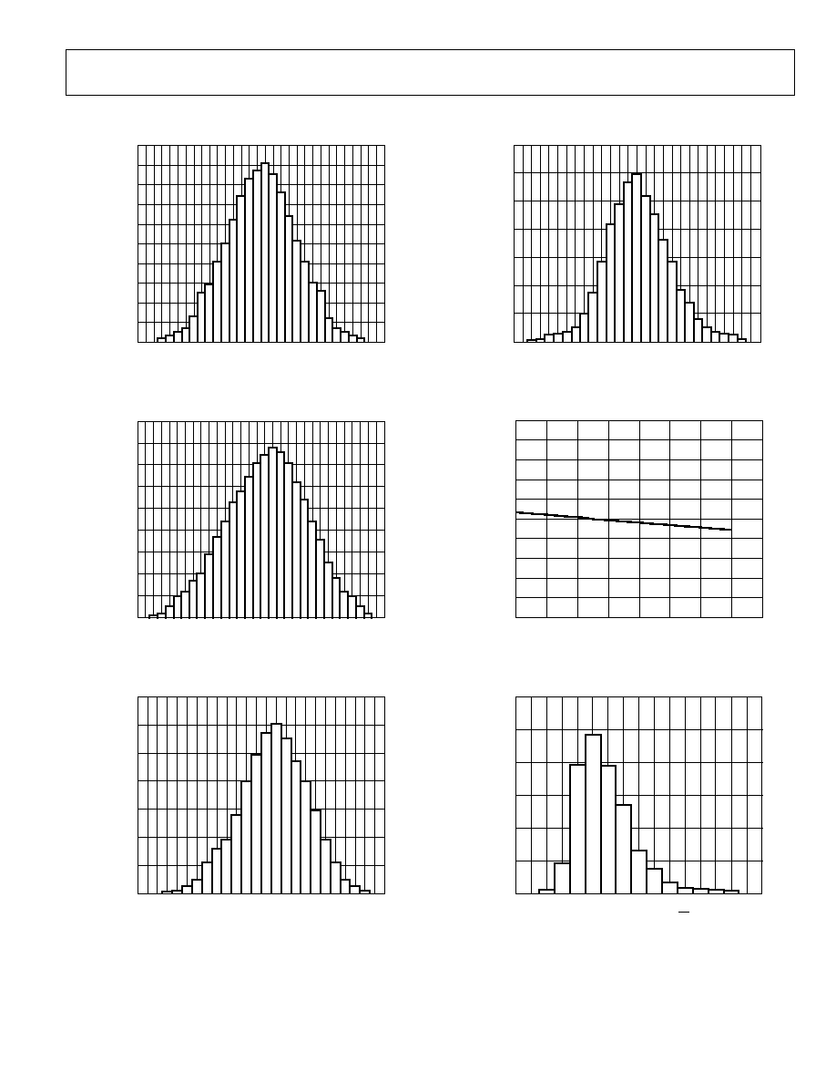
TYPICAL PERFORMANCE CHARACTERISTICS
V
P
E
RCE
NT OF P
ARTS
10
9
7
8
6
5
4
3
2
1
0
1.33
1.37
1.41
1.45
1.49
1.53
1.57
1.61
Figure 2. X-Axis Zero g BIAS Output Distribution
V
P
E
RCE
NT OF P
ARTS
9
7
8
6
5
4
3
2
1
0
1.33
1.37
1.41
1.45
1.49
1.53
1.57
1.61
Figure 3. Y-Axis Zero g BIAS Output Distribution
V/g
P
E
RCE
NT OF P
ARTS
14
12
8
10
6
4
2
0
0.156
0.16
0.164
0.168
0.172
0.176
0.18
Figure 4. X-Axis Output Sensitivity Distribution at X
OUT
V/g
P
E
RCE
NT OF P
ARTS
14
12
8
10
6
4
2
0
0.153
0.157
0.165
0.169
0.161
0.173
0.177
0.181
Figure 5. Y-Axis Sensitivity Distribution at Y
OUT
TEMPERATURE ≠
∞C
SEN
SITIVITY
≠ %
90
92
94
96
98
100
102
104
106
108
110
10
0
30
20
40
60
50
80
70
Figure 6. Normalized Sensitivity vs. Temperature
NOISE DENSITY ≠
µg/Hz
P
E
RCE
NT OF P
ARTS
30
15
10
25
20
5
0
150
200
250
300
350
400
450
500
550
Figure 7. Noise Density Distribution
Rev. A | Page 5 of 12