Äîêóìåíòàöèÿ è îïèñàíèÿ www.docs.chipfind.ru
Small and Thin ±5 g Accelerometer
ADXL320
Rev. 0
Information furnished by Analog Devices is believed to be accurate and reliable.
However, no responsibility is assumed by Analog Devices for its use, nor for any
infringements of patents or other rights of third parties that may result from its use.
Specifications subject to change without notice. No license is granted by implication
or otherwise under any patent or patent rights of Analog Devices. Trademarks and
registered trademarks are the property of their respective owners.
One Technology Way, P.O. Box 9106, Norwood, MA 02062-9106, U.S.A.
Tel: 781.329.4700
www.analog.com
Fax: 781.326.8703
© 2004 Analog Devices, Inc. All rights reserved.
FEATURES
Small and thin
4 mm × 4 mm × 1.45 mm LFCSP package
2 mg resolution at 60 Hz
Wide supply voltage range: 2.4 V to 5.25 V
Low power: 350 µA at V
S
= 2.4 V (typ)
Good zero g bias stability
Good sensitivity accuracy
X-axis and Y-axis aligned to within 0.1° (typ)
BW adjustment with a single capacitor
Single-supply operation
10,000 g shock survival
Compatible with Sn/Pb and Pb-free solder processes
APPLICATIONS
Cost-sensitive motion- and tilt-sensing applications
Smart hand-held devices
Mobile phones
Sports and health-related devices
PC security and PC peripherals
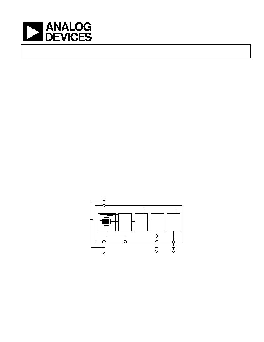
GENERAL DESCRIPTION
The ADXL320 is a low cost, low power, complete dual-axis
accelerometer with signal conditioned voltage outputs, which is
all on a single monolithic IC. The product measures
acceleration with a full-scale range of ±5 g (typical). It can also
measure both dynamic acceleration (vibration) and static
acceleration (gravity).
The ADXL320's typical noise floor is 250 µg/Hz, allowing
signals below 2 mg to be resolved in tilt-sensing applications
using narrow bandwidths (<60 Hz).
The user selects the bandwidth of the accelerometer using
capacitors C
X
and C
Y
at the X
OUT
and Y
OUT
pins. Bandwidths of
0.5 Hz to 2.5 kHz may be selected to suit the application.
The ADXL320 is available in a very thin 4 mm × 4 mm ×
1.45 mm, 16-lead, plastic LFCSP.
FUNCTIONAL BLOCK DIAGRAM
04993-001
ADXL320
SENSOR
+3V
OUTPUT
AMP
OUTPUT
AMP
COM
ST
V
S
C
DC
DEMOD
AC
AMP
R
FILT
32k
X
OUT
C
X
Y
OUT
C
Y
R
FILT
32k
Figure 1.

ADXL320
Rev. 0 | Page 2 of 16
TABLE OF CONTENTS
Specifications..................................................................................... 3
Absolute Maximum Ratings............................................................ 4
ESD Caution.................................................................................. 4
Pin Configuration and Function Descriptions............................. 5
Typical Performance Characteristics (V
S
= 3.0 V) ....................... 7
Theory of Operation ...................................................................... 11
Performance ................................................................................ 11
Applications..................................................................................... 12
Power Supply Decoupling ......................................................... 12
Setting the Bandwidth Using C
X
and C
Y
................................. 12
Self-Test ....................................................................................... 12
Design Trade-Offs for Selecting Filter Characteristics: The
Noise/BW Trade-Off.................................................................. 12
Use with Operating Voltages Other than 3 V ............................. 13
Use as a Dual-Axis Tilt Sensor ................................................. 13
Outline Dimensions ....................................................................... 14
Ordering Guide .......................................................................... 14
REVISION HISTORY
9/04--Revision 0: Initial Version

ADXL320
Rev. 0 | Page 3 of 16
SPECIFICATIONS
1
T
A
= 25°C, V
S
= 3 V, C
X
= C
Y
= 0.1 µF, Acceleration = 0 g, unless otherwise noted.
Table 1.
Parameter Conditions
Min
Typ
Max
Unit
SENSOR INPUT
Each axis
Measurement Range
±5
g
Nonlinearity
% of full scale
±0.2
%
Package Alignment Error
±1
Degrees
Alignment Error
X sensor to Y sensor
±0.1
Degrees
Cross Axis Sensitivity
±2
%
SENSITIVITY (RATIOMETRIC)
2
Each
axis
Sensitivity at X
OUT
, Y
OUT
V
S
= 3 V
156
174
192
mV/g
Sensitivity Change due to Temperature
3
V
S
= 3 V
0.01
%/°C
ZERO g BIAS LEVEL (RATIOMETRIC)
Each axis
0 g Voltage at X
OUT
, Y
OUT
V
S
= 3 V
1.3
1.5
1.7
V
0 g Offset Versus Temperature
±0.6
mg/°C
NOISE
PERFORMANCE
Noise Density
@ 25°C
250
µg/Hz rms
FREQUENCY RESPONSE
4
C
X
, C
Y
Range
5
0.002
10
µF
R
FILT
Tolerance
32 ± 15%
k
Sensor Resonant Frequency
5.5
kHz
SELF-TEST
6
Logic Input Low
0.6
V
Logic Input High
2.4
V
ST Input Resistance to Ground
50
k
Output Change at X
OUT
, Y
OUT
Self-test 0 to 1
55
mV
OUTPUT
AMPLIFIER
Output Swing Low
No load
0.3
V
Output Swing High
No load
2.5
V
POWER
SUPPLY
Operating Voltage Range
2.4
5.25
V
Quiescent Supply Current
0.48
mA
Turn-On Time
7
20 ms
TEMPERATURE
Operating Temperature Range
-20
70
°C
1
All minimum and maximum specifications are guaranteed. Typical specifications are not guaranteed.
2
Sensitivity is essentially ratiometric to V
S
. For V
S
= 2.7 V to 3.3 V, sensitivity is 154 mV/V/g to 194 mV/V/g typical.
3
Defined as the output change from ambient-to-maximum temperature or ambient-to-minimum temperature.
4
Actual frequency response controlled by user-supplied external capacitor (C
X
, C
Y
).
5
Bandwidth = 1/(2 × × 32 k × C). For C
X
, C
Y
= 0.002 µF, bandwidth = 2500 Hz. For C
X
, C
Y
= 10 µF, bandwidth = 0.5 Hz. Minimum/maximum values are not tested.
6
Self-test response changes cubically with V
S
.
7
Larger values of C
X
, C
Y
increase turn-on time. Turn-on time is approximately 160 × C
X
or C
Y
+ 4 ms, where C
X
, C
Y
are in µF.
ADXL320
Rev. 0 | Page 4 of 16
ABSOLUTE MAXIMUM RATINGS
Table 2.
Parameter Rating
Acceleration (Any Axis, Unpowered)
10,000 g
Acceleration (Any Axis, Powered)
10,000 g
V
S
-0.3 V to +7.0 V
All Other Pins
(COM - 0.3 V) to
(V
S
+ 0.3 V)
Output Short-Circuit Duration
(Any Pin to Common)
Indefinite
Operating Temperature Range
-55°C to +125°C
Storage Temperature
-65°C to +150°C
Stresses above those listed under Absolute Maximum Ratings
may cause permanent damage to the device. This is a stress
rating only; functional operation of the device at these or any
other conditions above those indicated in the operational
section of this specification is not implied. Exposure to absolute
maximum rating conditions for extended periods may affect
device reliability.
ESD CAUTION
ESD (electrostatic discharge) sensitive device. Electrostatic charges as high as 4000 V readily accumulate
on the human body and test equipment and can discharge without detection. Although this product features
proprietary ESD protection circuitry, permanent damage may occur on devices subjected to high energy
electrostatic discharges. Therefore, proper ESD precautions are recommended to avoid performance
degradation or loss of functionality.
ADXL320
Rev. 0 | Page 5 of 16
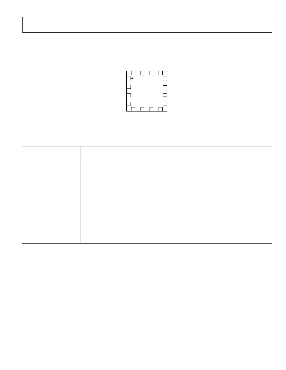
PIN CONFIGURATION AND FUNCTION DESCRIPTIONS
NC
X
OUT
ST
NC
COM
Y
OUT
NC
NC
COM COM COM
NC
NC
V
S
V
S
NC
NC = NO CONNECT
ADXL320
TOP VIEW
(Not to Scale)
04993-022
Figure 2. Pin Configuration
Table 3. Pin Function Descriptions
Pin No.
Mnemonic
Description
1
NC
Do Not Connect
2 ST
Self-Test
3 COM
Common
4
NC
Do Not Connect
5 COM
Common
6 COM
Common
7 COM
Common
8
NC
Do Not Connect
9
NC
Do Not Connect
10 Y
OUT
Y Channel Output
11
NC
Do Not Connect
12 X
OUT
X Channel Output
13
NC
Do Not Connect
14 V
S
2.4 V to 5.25 V
15 V
S
2.4 V to 5.25 V
16
NC
Do Not Connect
Document Outline
- FEATURES
- APPLICATIONS
- FUNCTIONAL BLOCK DIAGRAM
- GENERAL DESCRIPTION
- TABLE OF CONTENTS
- þÿ
- þÿ
- þÿ
- þÿ
- þÿ
- þÿ
- þÿ