Äîêóìåíòàöèÿ è îïèñàíèÿ www.docs.chipfind.ru
±75°/s Single Chip Yaw Rate
Gyro with Signal Conditioning
ADXRS401
Rev. 0
Information furnished by Analog Devices is believed to be accurate and reliable.
However, no responsibility is assumed by Analog Devices for its use, nor for any
infringements of patents or other rights of third parties that may result from its use.
Specifications subject to change without notice. No license is granted by implication
or otherwise under any patent or patent rights of Analog Devices. Trademarks and
registered trademarks are the property of their respective owners.
One Technology Way, P.O. Box 9106, Norwood, MA 02062-9106, U.S.A.
Tel: 781.329.4700
www.analog.com
Fax: 781.326.8703
© 2004 Analog Devices, Inc. All rights reserved.
FEATURES
Complete rate gyroscope on a single chip
Z-axis (yaw-rate) response
High vibration rejection over wide frequency
2000 g powered shock survivability
Self-test on digital command
Temperature sensor output
Precision voltage reference output
Absolute rate output for precision applications
5 V single-supply operation
Ultra small and light (< 0.15 cc, < 0.5 gram)
APPLICATIONS
GPS navigation systems
Image stabilization
Inertial measurement units
Platform stabilization
GENERAL DESCRIPTION
The ADXRS401 is a functionally complete and low cost angular
rate sensor (gyroscope), integrated with all of the required
electronics on one chip. It is manufactured using Analog
Devices' surface-micromachining technique, the same high
volume BIMOS process used for high reliability automotive
airbag accelerometers. It is available in a 7 mm × 7 mm × 3 mm
BGA surface-mount package.
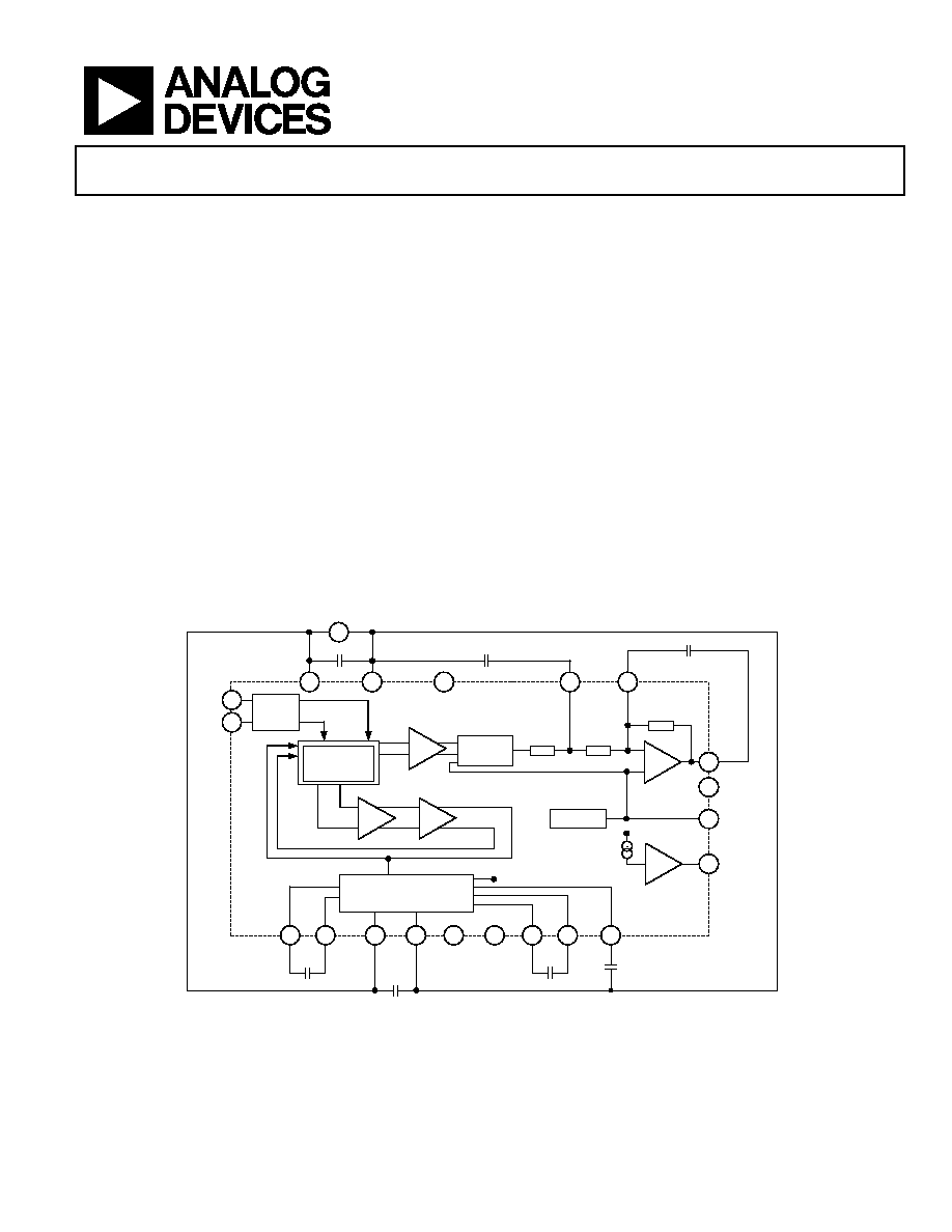
The output signal, RATEOUT (1B, 2A), is a voltage proportional
to angular rate about the axis normal to the top surface of the
package (see Figure 2). A single external resistor can be used to
lower the scale factor. An external capacitor is used to set the
bandwidth. Other external capacitors are required for operation
(see Figure 1).
A precision reference and a temperature output are also
provided for compensation techniques. Two digital self-test
inputs electromechanically excite the sensor to test proper
operation of both sensors and the signal conditioning circuits.
FUNCTIONAL BLOCK DIAGRAM
5G
4G
3A
5V
2G
1F
7F
6A
7D
7C
7B
1C
4A
5A
7E
6G
1D
2A
1E
3G
1B
PDD
12V
+
ADXRS401
1
µ
F
22nF
100nF
22nF
CP2
CP1
PGND
CP4
CP3
CP5
CHARGE PUMP/REG.
TEMP
PTAT
RATEOUT
2.5V
DEMOD
RATE
SENSOR
SELF
TEST
100nF
100nF
CMID
AGND
AVCC
ST1
ST2
CORIOLIS SIGNAL CHANNEL
S
SEN
2
R
SEN
1
C
OUT
R
OUT
180k
1%
9k
±
35%
9k
±
35%
SUMJ
2.5V REF
RESONATOR LOOP
04992-001
Figure 1.

ADXRS401
Rev. 0 | Page 2 of 12
TABLE OF CONTENTS
Specifications..................................................................................... 3
Absolute Maximum Ratings............................................................ 4
Rate-Sensitive Axis ....................................................................... 4
Pin Configuration and Function Descriptions............................. 5
Typical Performance Characteristics ............................................. 6
Theory of Operation ........................................................................ 8
Supply and Common Considerations ....................................... 8
Setting Bandwidth ........................................................................ 9
Increasing Measurement Range ................................................. 9
Temperature Output and Calibration ........................................ 9
Use with a Supply-Ratiometric ADC....................................... 10
Null Adjust................................................................................... 10
Self-Test Function....................................................................... 10
Acceleration Sensitivity ............................................................. 10
Outline Dimensions ....................................................................... 12
Ordering Guide........................................................................... 12
REVISION HISTORY
7/04--Revision 0: Initial Version

ADXRS401
Rev. 0 | Page 3 of 12
SPECIFICATIONS
@T
A
= 25°C, V
s
= 5 V, bandwidth = 80 Hz (C
OUT
= 0.01 µF), angular rate = 0°/s, ± 1 g, unless otherwise noted.
Table 1.
Parameter Conditions
Min
Typ
Max
Unit
SENSITIVITY
Top view clockwise rotation is positive output
Dynamic Range
1
Full-scale range,
-40
°
C to +85
°
C
±75
°/s
Scale Factor
-40
°
C to +85
°
C
12.75 15
17.25
mV/°/s
Nonlinearity
Best fit straight line
0.1
% of FS
NULL
Initial Null
2.50
V
Turn-On Time
Power on to ± ½°/s of final
35
ms
Linear Acceleration Effect
Any axis
0.2
°/s/g
NOISE PERFORMANCE
Rate Noise
@ 10 Hz bandwidth
3
mV (rms)
FREQUENCY RESPONSE
3 dB Bandwidth
2
(User Selectable)
22 nF as C
OUT
(see Setting Bandwidth section)
40
Hz
Sensor Resonant Frequency
14
kHz
SELF TEST
ST1 RATEOUT Response
3
ST1 pin from Logic 0 to 1
-800
mV
ST2 RATEOUT Response
3
ST2 pin from Logic 0 to 1
+800
mV
Logic 1 Input Voltage
Standard high logic level definition
3.3
V
Logic 0 Input Voltage
Standard low logic level definition
1.7
V
Input Impedance
To common
50
k
TEMPERATURE SENSOR
V
OUT
at 298K
2.50
V
Max Current Load on Pin
Source to common
50
µA
Scale Factor
Proportional to absolute temperature
8.4
mV/K
OUTPUT DRIVE CAPABILITY
Output Voltage Swing
I
OUT
= ±100 µA
0.25
V
S
0.25
V
Capacitive Load Drive
1000
pF
2.5 V REFERENCE
Voltage Value
2.5
V
Load Drive to Ground
Source
200
µA
Load Regulation
0 < I
OUT
< 200 µA
5.0
mV/mA
POWER SUPPLY
Operating Voltage Range
4.75
5.00
5.25
V
Quiescent Supply Current
6.0
8.0
mA
TEMPERATURE RANGE
Operating Temperature Range
-40
+85 °C
1
Dynamic range is the maximum full-scale measurement range possible, including output swing range, initial offset, sensitivity, offset drift, and sensitivity drift at 5 V
supplies.
2
Frequency at which response is 3 dB down from dc response with specified compensation capacitor value. Internal pole forming resistor is 180 k
. See the S
section.
etting
Bandwidth
3
Self-test response varies with temperature. See the
section for details.
Self-Test Function
ADXRS401
Rev. 0 | Page 4 of 12
ABSOLUTE MAXIMUM RATINGS
Table 2.
Parameter Rating
Acceleration (Any Axis, Unpowered, 0.5 ms)
2000 g
Acceleration (Any Axis, Powered, 0.5 ms)
2000 g
+V
S
-0.3 V to +6.0 V
Output Short-Circuit Duration (Any Pin to
Common)
Indefinite
Operating Temperature Range
-55°C to +125°C
Storage Temperature
-65°C to +150°C
Stresses above those listed under the Absolute Maximum
Ratings may cause permanent damage to the device. This is a
stress rating only; functional operation of the device at these or
any other conditions above those indicated in the operational
section of this specification is not implied. Exposure to absolute
maximum rating conditions for extended periods may affect
device reliability.
Applications requiring more than 200 cycles to MIL-STD-883
Method 1010 Condition B (55°C to +125°C) require underfill
or other means to achieve this requirement.
Drops onto hard surfaces can cause shocks of greater than
2000 g and exceed the absolute maximum rating of the device.
Care should be exercised in handling to avoid damage.
ESD CAUTION
ESD (electrostatic discharge) sensitive device. Electrostatic charges as high as 4000 V readily accumulate on
the human body and test equipment and can discharge without detection. Although this product features
proprietary ESD protection circuitry, permanent damage may occur on devices subjected to high energy
electrostatic discharges. Therefore, proper ESD precautions are recommended to avoid performance
degradation or loss of functionality.
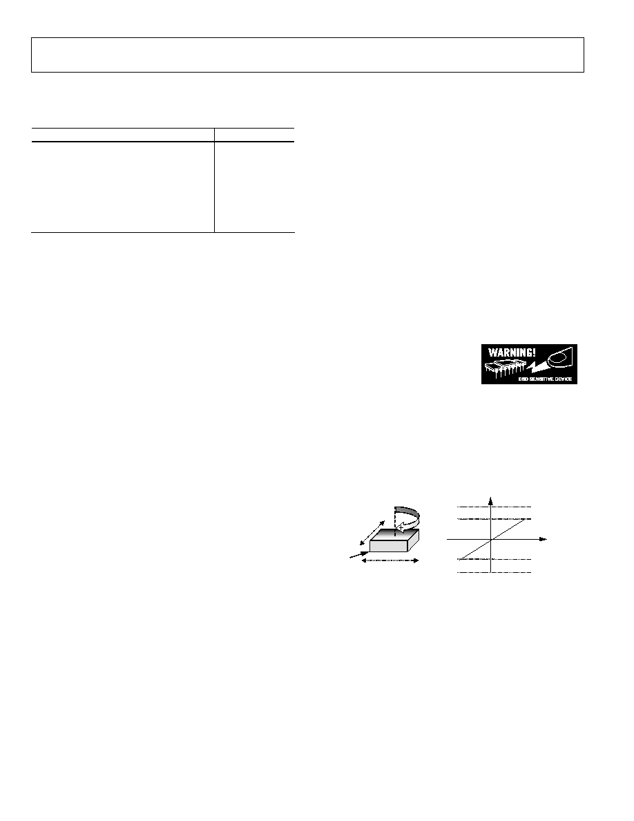
RATE-SENSITIVE AXIS
This Z-axis rate-sensing device is also called a yaw-rate sensing
device. It produces a positive-going output voltage for clockwise
rotation about the axis normal to the package top (clockwise
when looking down at the package lid).
2.5V
RATE
AXIS
RATEOUT
RATE IN
GND
4.75V
0.25V
LATERAL AXIS
A B C D E F G
7
A1
1
LONGITUDINAL
AXIS
V
CC
= 5V
04992-002
Figure 2. RATEOUT Signal Increases with Clockwise Rotation
ADXRS401
Rev. 0 | Page 5 of 12
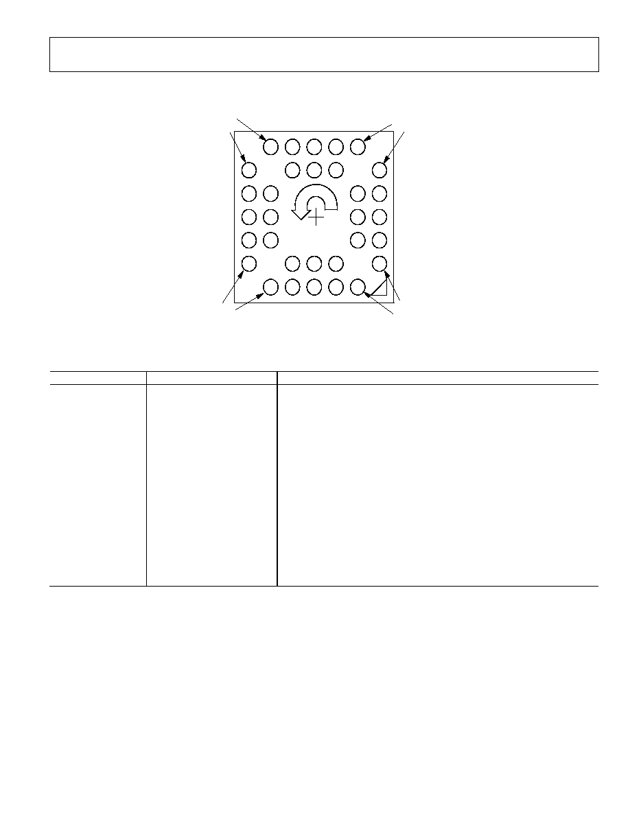
PIN CONFIGURATION AND FUNCTION DESCRIPTIONS
04992-020
AGND
TEMP
ST2
ST1
PGND
AVCC
CP1
CP2
CP4
RATEOUT
G
F
E
D
C
B
A
7
6
5
4
3
2
1
CP5
CP3
PDD
CMID SUMJ
2.5V
Figure 3. BGA-32 (Bottom View)
Table 3. Pin Function Descriptions
Pin No.
Mnemonic
Description
6D, 7D
CP5
HV Filter Capacitor to Ground 1
µ
F 20 V minimum
6A, 7B
CP4
Charge Pump Capacitor 22 nF
6C, 7C
CP3
Charge Pump Capacitor 22 nF
5A, 5B
CP1
Charge Pump Capacitor 22 nF
4A, 4B
CP2
Charge Pump Capacitor 22 nF
3A, 3B
AVCC
+ Analog Supply
1B, 2A
RATEOUT
Rate Signal Output
1C, 2C
SUMJ
Output Amp Summing Junction
1D, 2D
CMID
HF Filter Capacitor 100 nF
1E, 2E
V2.5
2.5 V Precision Reference
1F, 2G
AGND
Analog Supply Return
3F, 3G
TEMP
Temperature Voltage Output
4F, 4G
ST2
Self-Test for Sensor 2
5F, 5G
ST1
Self-Test for Sensor 1
6G, 7F
PGND
Charge Pump Supply Return
6E, 7E
PDD
+ Charge Pump Supply
Document Outline