
AIC1761/1766
BATTERY CHARGE CONTROLLER
SPEC NO: DS-1761-02
ANALOG INTEGRATIONS CORPORATION
www.analog.com.tw
4F, 9 Industry E. 9th Road, Science-based Industrial Park , Hsinchu, Taiwan, R.O.C. TEL: (8863)577-2500 FAX:(8863)577-2510
1
FEATURES
Reliable Fast Charge Control of NiMH/NiCd Bat-
teries.
Quick and Easy Testing for Production.
Fast Charge Termination by:
1. Accurate -
V Detection Level with Respect to
Peak Battery Voltage Value.
AIC1761 ....................................... -1%
AIC1766 ...................................... -0.25%
2. Peak Voltage Timer (0
V).
Adjustable Fast Charge Safety Timer.
Protection against Temperature Fault.
Protection against Short-Circuited and Open Bat-
teries.
Wide Operation Voltage Range: 9V to 18V, no Ex-
tra Regulator Needed.
Large Battery Voltage Detection Range: 0.65V to
3.7V.
LED Drivers to Indicate Charge Status or Fault
Conditions.
Voltage Reference Output.
Space-Saving Packages:
8-PIN DIP, SO
14-PIN DIP, SO
APPLICATIONS
Battery Chargers for :
Mobile Phones
Notebook and Laptop Personal Computers
Portable Power Tools and Toys
Portable Communication Equipments
Portable Video and Stereo Equipments
DESCRIPTION
The AIC1761/1766 fast charge controller IC is
designed for intelligent charging of NiMH or NiCd
batteries without overcharging. It detects a voltage
drop (-
V) occurring in the final stage of a fast
charging cycle and correspondingly controls the
charging current. Fast charge can also be cut off
by a peak voltage timer (0
V).
The detection of -
V is a very reliable method to
terminate fast charging for NiMH and NiCd batter-
ies. The AIC1761/1766 uses -
V detection as one
of primary decisions for fast charge cut-off. The -
V value for the AIC1761 is as small as 16mV per
cell, suitable for NiCd batteries. The
-
V value for the AIC1766 is as small as 4mV per
cell, particularly suitable for NiMH as well as the
NiCd batteries. The peak voltage timer is particu-
larly useful when the voltage drop at the end of
charge for some batteries, e.g. NiMH cells, is not
pronounced enough for reliable detection. An ad-
justable safety timer (3 settings) is used as a back-
up termination method. Provisions are made with
the AIC1761/1766 to prevent fast charge under
temperature fault conditions. Two LED outputs are
used to indicate the charging status. Another flash
LED output can be used alone to indicate charge
status.
AC mode allows the battery to drive its loads while
being charged. Test mode is provided to dramati-
cally reduce production test time.

AIC1761/1766
BATTERY CHARGE CONTROLLER
SPEC NO: DS-1761-02
ANALOG INTEGRATIONS CORPORATION
www.analog.com.tw
4F, 9 Industry E. 9th Road, Science-based Industrial Park , Hsinchu, Taiwan, R.O.C. TEL: (8863)577-2500 FAX:(8863)577-2510
2
TYPICAL APPLICATION CIRCUIT
9.1V
1N4148
+
+
C1
0.33
1W
R8
470
10
µ
F
V
IN
12 ~ 15 V
GREEN
LED2
RED
LED1
1N4148
D1
120
0.5W
R1
R9
1K
R10
1K
100
µ
F
C7
ZD1
R5
D3
R2
1K
C2
+
+
1
µ
F
C3
100K
R3
220
µ
F
R7
470pF
AIC1563
IS
BST
FB
VCC
GND
TC
SE
SC
1
2
3
4
5
6
7
8
D2
C4
1N5819
*Fast Charge Current= (0.3/RS) A
8
VREF
7
6
5
LED
VOUT
VDD
4.7
µ
F
0.1
µ
F
150K
AIC1761/66
C6
R4
C5
51K
4
3
2
1
MODE
TIMER
GND
VBT
+
L1
1N5819
1K
BATTERY
D4
3 ~ 5 CELLS
220
µ
H
*RS
Simple Battery Charger for NiMH / NiCd Battery
ORDERING INFORMATION
AIC176X-XXXX
ORDER NUMBER
TOP VIEW
AIC1761-CN08
AIC1766-CN08
(PLASTIC DIP)
AIC1761-CS08
AIC1766-CS08
(PLASTIC SO)
PIN CONFIGURATION
AIC1761-CN14
AIC1766-CN14
(PLASTIC DIP)
AIC1761-CS14
AIC1766-CS14
(PLASTIC SO)
1
3
4
2
8
VREF
6
VOUT
5
LED
7
VDD
GND
TIMER
MODE
VBT
TOP VIEW
14
1
3
4
2
5
7
6
12
11
13
10
8
9
VBT
GND
NC
NC
VDD
VREF
VNTC
TIMER
MODE
LED
GND
NC
FLASH
VOUT
VERSION
08: 8 PIN VERSION
14: 14 PIN VERSION
PACKAGE TYPE
N: PLASTIC DIP
S: SMALL OUTLINE
TEMPERATURE RANGE
C=0
∞
C~70
∞
C
-
V DETECTION LEVEL
1: -1%
6: -0.25%
ABSOLUTE MAXIMUM RATINGS
Supply Voltage
................................................................................................................
18V
DC Voltage Applied on any Pin
...........................................................................................
18V
Sink Current of VOUT Pin, LED Pin, and FLASH Pin
.......................................................
20mA
Operating Temperature Range
...............................................................................
0
∞
C to 70
∞
C
Storage Temperature Range .............................................................................. -65
∞
C to 150
∞
C

AIC1761/1766
BATTERY CHARGE CONTROLLER
SPEC NO: DS-1761-02
ANALOG INTEGRATIONS CORPORATION
www.analog.com.tw
4F, 9 Industry E. 9th Road, Science-based Industrial Park , Hsinchu, Taiwan, R.O.C. TEL: (8863)577-2500 FAX:(8863)577-2510
3
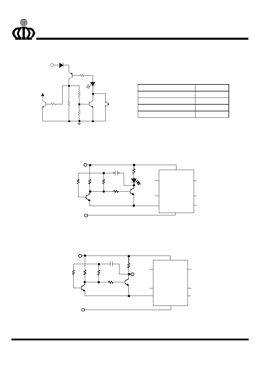
TEST CIRCUIT
+
+V
DD
+V
DD
MODE
FLASH
LED
VOUT
VDD
Voltage
Source
390K
R1
4.
7
µ
F
C1
150K
R2
20K
R5
4.7K
R4
VNTC
VREF
TIMER
0.1
µ
F
C2
150K
R3
GND
VBT
-
100
µ
F
C4
1.5K
R6
1.5K
R7
0.1
µ
F
C3
1.5K
R8
+
+
ELECTRICAL CHARACTERISTICS
(V
DD
=12.5V, Ta=25
∞
∞
∞
∞
C, unless otherwise specified.)
PARAMETER
TEST CONDITIONS SYMBO
L
MIN.
TYP.
MAX.
UNIT
Supply Voltage
V
DD
9
18
V
Supply Current
I
DD
1.5
mA
-
V Detection Level w.r.t.* Peak
Value
AIC1761
AIC1766
-1
-0.25
%
%
Voltage Protection Limits
Battery Low
Battery High
V
BT
0.5
3.5
0.65
3.7
0.8
3.9
V
V
Input Impedance of TIMER Pin
Z
TIMER
100
K
Input Impedance of MODE Pin
Z
MODE
100
K
Output Resistance of LED Pin
Fast Charge
Trickle Charge
R
LED
1
25
M
Output Resistance of VOUT Pin
Fast Charge
Trickle Charge
R
VOUT
1
25
M
FLASH pin
Output Resistance
Frequency
Duty Cycle
Fast Charge
Trickle Charge
R
FLASH
F
FLASH
D
FLASH
25
1
50
Hz
%
Reference Voltage
Reference Source Current
V
REF
I
REF
1.5
5.85
V
mA
Temperature Fault Voltage
Limits as Fraction of V
REF
Under-Temperature
Over-Temperature
NTCL
NTCH
0.60
0.15
0.7
0.2
0.80
0.25
V
REF
V
REF
*w.r.t.: with respect to
AIC1761/1766
BATTERY CHARGE CONTROLLER
SPEC NO: DS-1761-02
ANALOG INTEGRATIONS CORPORATION
www.analog.com.tw
4F, 9 Industry E. 9th Road, Science-based Industrial Park , Hsinchu, Taiwan, R.O.C. TEL: (8863)577-2500 FAX:(8863)577-2510
4
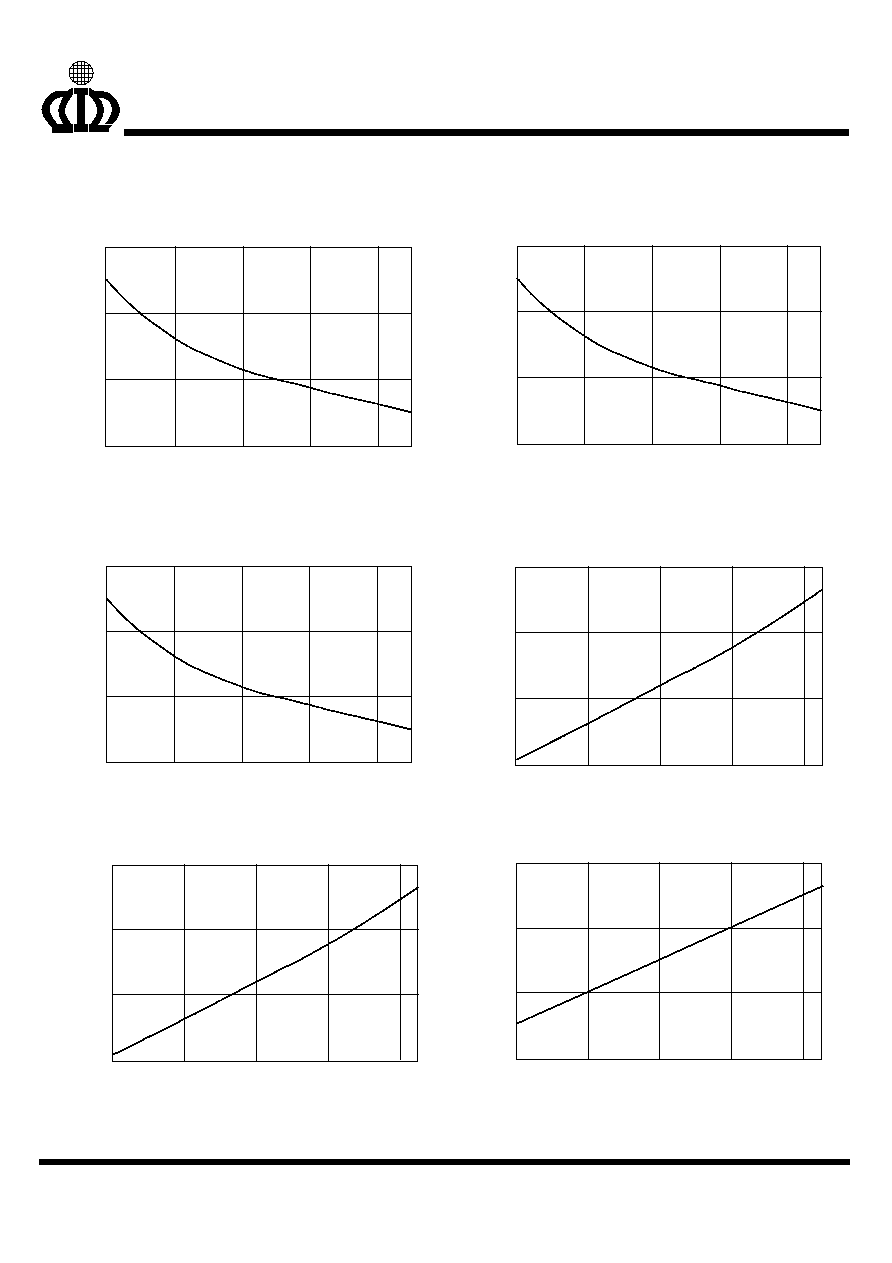
TYPICAL PERFORMANCE CHARACTERISTICS
V
DD
(V)
Output Resistance of VOUT pin vs Power
Supply Voltage (Fast Charge Mode)
R
VOUT
(
)
9
11
13
15
17
18
20
24
28
32
V
DD
(V)
Output Resistance of LED pin vs Power
Supply Voltage (Trickle Charge Mode)
R
LED
(
)
9
11
13
15
17
18
20
24
28
32
V
DD
(V)
Output Resistance of FLASH pin vs Power
Supply Voltage (Fast Charge Mode)
9
11
13
15
17
18
20
24
28
32
R
FL
AS
H
(
)
Output Resistance of VOUT pin vs
Temperature (Fast Charge Cycle)
Temperature (
∞
C)
R
VO
UT
(
)
0
20
40
60
80
26
30
34
22
Output Resistance of LED pin vs Temperature
(Trickle Charge Cycle)
Temperature (
∞
C)
R
LE
D
(V
)
0
20
40
60
80
22
26
30
34
V
REF
Reference Voltage vs Temperature
Temperature (
∞
C)
0
20
40
60
80
5.6
5.8
6.0
6.2
V
REF
(V
)

AIC1761/1766
BATTERY CHARGE CONTROLLER
SPEC NO: DS-1761-02
ANALOG INTEGRATIONS CORPORATION
www.analog.com.tw
4F, 9 Industry E. 9th Road, Science-based Industrial Park , Hsinchu, Taiwan, R.O.C. TEL: (8863)577-2500 FAX:(8863)577-2510
5
TYPICAL PERFORMANCE CHARACTERISTICS
(CONTINUED)
V
BT
(High) Limit vs Temperature
(V)
Temperature (
∞
C)
V
BT
(V
)
0
20
40
60
80
3.4
3.6
3.8
3.7
3.5
V
BT
(Low) Limit vs Temperature
Temperature (
∞
C)
0
20
40
60
80
0.55
0.63
0.71
0.59
V
BT
(V
)
0.67
Safety Timer vs Temperature
(MODE pin = V
DD
)
Temperature (
∞
C)
0
20
40
60
80
35
37
39
41
43
45
S
a
fet
y
Ti
m
e
r
(
m
i
n
.)
BLOCK DIAGRAM
CHARGE CONTROL
STATE MACHINE
13-Bit
ADC
Mode
Select
Timing
Control
Oscillator
Power On
Reset
+
-
VR1
VR2
LED
VDD
VREF
Voltage
Regulator
GND
+
-
VR3
VR4
+
-
-
+
VBT
VOUT
MODE
TIMER
VNTC (for 14 pin version)
FLASH
(for 14 pin version)
AIC1761/1766
BATTERY CHARGE CONTROLLER
SPEC NO: DS-1761-02
ANALOG INTEGRATIONS CORPORATION
www.analog.com.tw
4F, 9 Industry E. 9th Road, Science-based Industrial Park , Hsinchu, Taiwan, R.O.C. TEL: (8863)577-2500 FAX:(8863)577-2510
6
PIN DESCRIPTIONS
VDD PIN
- Supply voltage input.
GND PIN
- Ground.
VBT PIN
- Input, to sense battery voltage.
MODE PIN - Input, to set IC operation mode.
TIMER PIN - Input, for safety timer control.
VREF PIN - Voltage reference output.
LED PIN
- Output, for LED indicator.
VOUT PIN - Output, for LED indicator.
FLASH PIN - Output, for LED indicator.
(Available for 14-pin version only.)
VNTC PIN - Input, for temperature protection.
(Available for 14-pin version only.)
APPLICATION INFORMATIONS
BATTERY PROPERTIES
The basic principle of rechargeable battery sys-
tems, including NiMH and NiCd cells, is that the
processes of charge and discharge are reversible.
The charge characteristics of NiMH and NiCd
cells look similar in that (1) the cell voltage at the
end of charge drops and (2) the cell temperature
increases rapidly near the end of charge. Fig. 1
shows the charge voltage and charge tempera-
ture characteristics of NiMH and NiCd cells. No-
tice that the cell voltage decline of NiMH cells at
the end of charge is less pronounced than for
NiCd cells.
NiMH
Time (min.)
C
e
ll V
o
lt
a
g
e
(
V
)
1.1
1.2
1.3
1.4
1.5
1.6
1.7
Voltage
20
40
50
60
70
80
C
e
l
l
T
e
m
p
er
at
ur
e (
∞
C)
40
60
100
80
0
20
NiCd
Charge Current=1C
NiMH
NiCd
Temperature
30
Fig.
1
Typical Charge Characteristics of
NiMH/NiCd Battery
Fast-charge batteries are available where re-
charging takes for only 1 hour or less with a sim-
ple control circuit. One main purpose of the con-
trol circuit is to terminate the fast-charge process
to prevent the temperature and internal pressure
of the battery cell from building up to a damaging
level which degrades or even destroys the battery
cell.
The AIC1761/1766 is a battery fast charge con-
troller IC that utilizes the following methods to
terminate the fast charge process for NiMH or
NiCd battery cells:
Negative delta voltage cutoff (-
V).
Peak voltage timer cutoff (0
V).
Maximum temperature cutoff (TCO).
Maximum voltage cutoff (VCO).
Safety timer cutoff.
The principle of operation of the AIC1761/1766 is
described in the following section.
THE AIC1761/1766 OPERATION
When power is first applied to the charge system,
consisting of rechargeable battery cells, charge cur-
rent source, the AIC1761/1766 and its associated
external circuit, all internal digital circuit blocks of
the AIC1761/1766 are reset by internal power-on-
reset circuitry. The internal control unit then checks
the battery condition to prevent fast charge from
taking place under battery fault conditions, i.e. cell
voltage fault (V
BT
<0.65V or V
BT
>3.7V) or cell tem-
perature fault (
NTC>
NTCL or
NTC<
NTCH, for
the 14-pin version). Temperature fault limits corre-
sponding to
NTCL and
NTCH are determined by
an external thermistor divider circuit as included in
the Application Examples, Fig. 10. After the battery
passes condition fault checks, VOUT pin goes to
low to start fast charge while initial timer and safety
timer of the AIC1761/1766 start counting. Both the
negative delta voltage detector and the peak voltage
timer, however, are disabled until the initial timer
period in the initial stage of a charge circle elapses.
AIC1761/1766
BATTERY CHARGE CONTROLLER
SPEC NO: DS-1761-02
ANALOG INTEGRATIONS CORPORATION
www.analog.com.tw
4F, 9 Industry E. 9th Road, Science-based Industrial Park , Hsinchu, Taiwan, R.O.C. TEL: (8863)577-2500 FAX:(8863)577-2510
7
The AIC1761/1766 constantly monitors the voltage
at VBT pin, which rises as battery cells are being
fast-charged till battery full condition is nearly ap-
proached. The battery temperature is also con-
stantly being sensed to guard against abnormal
temperature situations. VOUT pin will be pulled high
by an external pull-up device and the fast charge
process be switched to trickle charge when one of
the following situations is encountered:
A negative delta voltage (-
V) at VBT pin is de-
tected when compared to its peak value. The
sampling rate of -
V detection is 2seconds/
sample. The detection level of -
V is -1% for the
AIC1761 and -0.25% for the AIC1766.
The battery voltage stays at its peak value for
the duration determined by the peak voltage
timer setting (0
V).
The VBT pin voltage exceeds the "high" battery
voltage protection limit (VCO).
The battery temperature, sensed by the ther-
mistor divider, exceeds the fault temperature
range (TCO).
The selected safety timer period has finished.
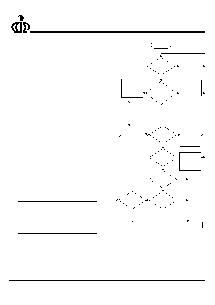
TIMER PIN
The TIMER pin can be used as follows to select
one of the preset safety timer period and its cor-
responding periods of initial timer and peak volt-
age timer:
TIMER
Pin
Safety
Timer
Peak Volt-
age Timer
Initial Timer
V
DD
40 min.
2 min.
1.5 min.
GND
80 min.
4 min.
3.0 min.
Floating
160 min.
8 min.
3.0 min.
Power ON
If
0.65V<V
BT
<3.7V
If
NTCL>
NTC
&
NTC>
NTCH
-
V detector &
peak voltage timer
start working after
initial period ends.
V
OUT
goes low for
fast charge,
safety timer starts
counting.
-
V detector &
peak voltage timer
working.
V
OUT
goes high for
trickle charge,
safety timer and
-
V detector reset.
V
OUT
goes high for
trickle charge ,
-
V detector reset,
safety timer stops.
If
0.65V<V
BT
<3.7V
If
safety timer period
has finished.
V
OUT
goes high
for trickle charge,
Safety Timer
and
-
V Detector
reset
V
OUT
goes to high, fast charge finished, and trickle charge start.
YES
YES
YES
YES
YES
YES
YES
NO
NO
NO
NO
NO
NO
NO
V
OUT
goes high
for trickle
charge, -
V
detector reset,
safety timer
stops.
If
NTCL>
NTC
&
NTC>
NTCH
If
peak voltage timer
period has finished.
If
-
V decline of VBT
is detected.
Fig. 2 Operation Chart of the AIC1761/1766

AIC1761/1766
BATTERY CHARGE CONTROLLER
SPEC NO: DS-1761-02
ANALOG INTEGRATIONS CORPORATION
www.analog.com.tw
4F, 9 Industry E. 9th Road, Science-based Industrial Park , Hsinchu, Taiwan, R.O.C. TEL: (8863)577-2500 FAX:(8863)577-2510
8
MODE PIN
The MODE pin determines the mode in which the
IC works:
MODE
Pin
Mode
Function
Floating
NORMAL
Normal operation
V
DD
TEST
1/512 safety timer
GND
AC
-
V detector reset,
timer stops (not reset)
The AIC1761/1766 will operate normally when the
MODE pin is left floating ( a 0.1
µ
F capacitor is re-
commended to be tied to MODE pin if the charge
circuit works in a noisy environment). The
AIC1761/1766 otherwise works in following ways
if the MODE pin is biased either to V
DD
or to GND:
(A) AC Mode (MODE pin biased to GND)
In the midst of normal charge operation, where
VBT pin voltage is in the range from 0.8V to 3.5V
and the preset safety timer has not run out, the
safety timer will stop if the MODE pin is somehow
pulled down to GND level. As long as the MODE
pin remains low, the VOUT pin stays ON and
LED pin OFF regardless whether the battery pack
voltage declines (-
V present) or not.
The AC mode can be activated by pulling MODE
pin to GND to avoid premature battery charge
cutoff due to fluctuating charge current source.
Switching MODE pin after the end of the safety
timer has no effect on the AIC1761/1766 display
outputs, i.e., VOUT pin stays OFF while LED pin
stays ON.
(B) TEST Mode (MODE pin biased to V
DD
)
An unique feature of the AIC1761/1766 is that it
can be put into a TEST mode by pulling the
MODE pin to V
DD
, allowing verification tests for
the AIC1761/1766 charge circuit to be performed
in a few tens of seconds, extremely valuable in fi-
nal phase of production.
When the AIC1761/1766 is in TEST mode, all the
internal timers are reduced by the following fac-
tors when compared to normal operation:
1. Safety timer reduced by 512 times.
2. Initial timer reduced by 512 times.
3. Peak timer reduced by 64 times.
One critical requirement needs to be observed for
-
V detector of the AIC1761/1766 to work prop-
erly in TEST mode. That is, VBT pin voltage must
be kept between approximately 2.8V to 3.3V,
rather than 0.8V to 3.5V in NORMAL mode.
If the TEST mode function is to be utilized in pro-
duction test, it has to be well planned and includ-
ed in circuit design phase to make the voltages of
VBT pin and MODE pin externally controllable. In
addition, an externally controllable TIMER pin can
further reduce test time required for testing the
AIC1761/1766 in TEST mode.
Fig. 3 shows the timing diagram for externally
controlled VBT, TIMER, and MODE pin voltages
of a recommended AIC1766 charge circuit pro-
duction test scheme, utilizing TEST mode func-
tion. Output waveforms of VOUT and LED pins
(and FLASH pin for 14 pin version) of a properly
functioning AIC1766 are also shown in the figure.
In timer segments 4, 8 and 10, VOUT pin should
change from ON to OFF, LED pin from OFF to
ON, and FLASH pin from ON to flashing output
(approximately 4 Hz). For the reset of time,
VOUT pin should remain ON, LED pin OFF, and
FLASH pin ON.

AIC1761/1766
BATTERY CHARGE CONTROLLER
SPEC NO: DS-1761-02
ANALOG INTEGRATIONS CORPORATION
www.analog.com.tw
4F, 9 Industry E. 9th Road, Science-based Industrial Park , Hsinchu, Taiwan, R.O.C. TEL: (8863)577-2500 FAX:(8863)577-2510
9
Init.
Timer
VBT
Set
Up
Peak Timer Test
(min.1.875S)
AC
Mode
VBT
Set Up
-
V Test
(min. 3.75S)
AC
Mode
Safety Timer Test
TIMER
Pin
MODE
Pin
VBT
Pin
VOUT
Pin
LED
Pin
FLASH
Pin
TIME
Section
VDD
VDD
2.98V
2.8V
3V
2.995V
3V
VDD/2
2.995V
*2.988V
GND
ON
OFF
ON
OFF
ON
4.27Hz
0.5S
1
0.4S
2
1.5S
3
1.5S
4
20mS
5
0.4S
6
4.7S
7
1.5S
8
20mS
9
2.5S
10
0.5S
11
GND
GND
* 2.972V for the AIC1761
Fig. 3 Timing Diagram of AIC1766 in Test Mode

AIC1761/1766
BATTERY CHARGE CONTROLLER
SPEC NO: DS-1761-02
ANALOG INTEGRATIONS CORPORATION
www.analog.com.tw
4F, 9 Industry E. 9th Road, Science-based Industrial Park , Hsinchu, Taiwan, R.O.C. TEL: (8863)577-2500 FAX:(8863)577-2510
10
The LED indicators work as the following table:
LED
PIN
VOUT
PIN
FLASH
PIN
Fast Charge
OFF
ON
ON
Trickle
Charge
ON
OFF
FLASH
V
BT
Abnormal
OFF
OFF
OFF
LED pin is used in conjunction with VOUT pin
while FLASH pin works alone.
Referring to the APPLICATION EXAMPLES (Fig.
10), the temperature limits beyond where the fast
charge is prohibited can be set by choosing values
for resistors and the thermistor of the thermistor
divider according to the following formula:
R18 = 3.57 R
T1
R
T2
/ (R
T1
-
R
T2
)
R19 = 10 R
T1
R
T2
/ (1.218 R
T1
-
11.2 R
T2
)
R
T1
: Thermistor resistance at low temperature
limit.
R
T2
: Thermistor resistance at high temperature
limit.
BATTERY VOLTAGE DIVIDER
To ensure proper operation of the AIC1761/1766,
selection of resistor values for battery voltage di-
vider must meet the following two crucial require-
ments:
1. When the battery pack is disconnected from
the charge circuitry, the voltage of VBT pin
must be higher than 4.0V or lower than 0.5 V to
put the AIC1761/1766 in reset status, where
VOUT and LED pins become high impedance
and FLASH pin (only for 14 pin version) goes to
high level.
2. When the battery pack is connected in normal
operation, the VBT pin voltage must remain in
the range of 0.8V to 3.5V even when the bat-
tery pack voltage reaches to its peak when
near full charge.
Take charging a 8-cell battery pack as an example.
The highest voltage would be 16V when fully
charged if the highest voltage of a fully charged
battery cell is assumed to be 2V. Since the VBT
pin voltage is restricted to be no higher than 3.5V,
the battery voltage divider ratio must be higher
than 3.57 (16V/3.5V -1). In other words, resistor
R14+R13 must be greater than 535K
if R15 is
150K
(refer to Fig. 4). When the battery pack is
disconnected from the charging circuitry the VBT
pin voltage must be higher than 4.0V, dictating
V
BAT
node voltage of the charging circuitry to be
higher than 18.3V (4V x 4.57). Practically, however,
the charging circuit supply voltage +V
IN
should be
higher than 18.5V in order to ensure proper op-
eration. In the case that supply voltage +V
IN
can
not meet this requirement, application circuit of Fig.
4 can be adopted to get around this problem.
9012
Q2
9012
Q1
27K
270K
270K
+V
IN
150K
390K
150K
4.7
µ
F
0.1
µ
F
0.1
µ
F
C1
150K
V
BAT
GND
VBT
R3
R2
R14
R13
R5
C2
R15
C3
R7
+
Fig. 4 Battery Voltage can be Raised to V
IN
- 0.9V
when being Charged.
CHARGER CIRCUIT DESIGN TIPS
1. A stable constant charge current is crucial for
reliable precision
-
V detection by the
AIC1761/1766 since fluctuation of the charge
current can cause fluctuation of the battery
terminal voltage due to battery internal series
resistance, which will likely result in errors
-
V detection by a properly functioning
AIC1761/1766.
2. To prevent the AIC1761/1766 from over-
voltage damage, make sure that none of
AIC1761/1766 pins sees any voltage beyond
the supply voltage, which needs to be be-
tween +9V and +18V.

AIC1761/1766
BATTERY CHARGE CONTROLLER
SPEC NO: DS-1761-02
ANALOG INTEGRATIONS CORPORATION
www.analog.com.tw
4F, 9 Industry E. 9th Road, Science-based Industrial Park , Hsinchu, Taiwan, R.O.C. TEL: (8863)577-2500 FAX:(8863)577-2510
11
3. If the battery charge current is high, say, over
1.5A, quality of circuit board layout and wiring
connection points become increasingly im-
portant in the charger circuit reliability.
4. Critical components need to meet adequate
rating to prevent heating-up of these compo-
nents from causing circuit malfunction.
5. Since the AIC1761/1766 is fabricated with
CMOS process, cares must be taken in han-
dling this device to avoid possible damage
from electro-static discharge.
EXPERIMENTAL RESULTS
Experiments have been conducted to verify the
AIC1761/1766 operation with NiCd and NiMH
battery cells of various brands. Actual results
shown in the following figures clearly indicate that
the negative delta voltage detector and the peak
voltage timer of the AIC1761/1766 have precisely
detected the tiny cell voltage drops or the cell volt-
age peaks and subsequently terminated the fast
charge process after batteries are fully charged.
The battery cell temperatures were all under
safety levels. Note that the fast charge for the
NiMH battery in Fig. 5 is terminated by the peak
voltage timer (0 V
) while the fast charge for the
NiCd battery in Fig. 6 is terminated by the -
V
detector.
Charge Time (min.)
C
e
l
l
Tempera
t
ure
(
∞
C)
C
e
l
l
V
o
l
t
age (V
)
0
20
40
60
80
1.2
1.3
1.4
1.5
1.6
Temperature
Voltage
Charge Current = 1A
Cell Capacity = 1000mAH
20
30
40
50
60
AIC1766
AIC1766
Fig. 5 Charge Characteristics of NiMH Battery
Both Fig. 5 and Fig. 6 were obtained by using the
AIC1766. Results of similar experiments by using the
AIC1761 are shown in Fig. 7 and Fig.8.
Charge Time (min.)
C
e
l
l
Tem
p
erat
ure(
∞
C)
C
e
ll
V
o
lta
g
e
(
V
)
20
30
40
50
60
0
20
40
60
80
1.3
1.4
1.5
1.6
1.7
Temperature
Voltage
Charge Current=0.7A
Cell Capacity=700mAH
AIC1766
Fig. 6 Charge Characteristics of NiCd Battery
Charge Time (min.)
C
e
l
l
V
o
l
t
age
(V
)
C
e
l
l
T
e
m
p
erat
ure
(
∞
C)
0
10
20
30
40
50
60
70
1.2
1.3
1.4
1.5
1.6
20
30
40
50
60
Temperature
Voltage
AIC1761
Charge Current = 1A
Cell Capacity =1000mAH
Fig. 7 Charge Characteristics of NiMH Battery
C
e
l
l
V
o
l
t
age(V
)
0
20
40
60
80
1.3
1.4
1.5
1.6
1.7
Charge Time (min.)
20
30
40
50
60
Voltage
C
e
l
l
T
e
mpera
t
ure
(
∞
C)
Temperature
Charge Current=0.7A
Cell Capacity=700mAH
AIC1761
Fig. 8 Charge Characteristics of NiCd Battery

AIC1761/1766
BATTERY CHARGE CONTROLLER
SPEC NO: DS-1761-02
ANALOG INTEGRATIONS CORPORATION
www.analog.com.tw
4F, 9 Industry E. 9th Road, Science-based Industrial Park , Hsinchu, Taiwan, R.O.C. TEL: (8863)577-2500 FAX:(8863)577-2510
12
APPLICATION EXAMPLES
+
+
+
*L1=MPP Core or Iron Powder Core
# 3~5 Cells for V
IN
=12~28V
**Fast Charge Current:(0.3/RS)A
# 3~6 Cells for V
IN
=15~28V
AIC1563
Q1
# BATTERY
C1
220
µ
F
35V
1nF
C2
R5
100K
1N5819
220
µ
H
*L1
R2
1.2K
0.33
1W
2N3904
R8
470
GREEN
LED2
RED
LED1
AIC1761/66
4.7
µ
F
C5
R9
1K
R10
1K
100
µ
F
C7
9.1V
ZD1
1K
R4
D3
1N4148
C6
0.1
µ
F
150K
R7
D4
51K
R6
4
3
2
1
8
7
6
5
LED
VOUT
VDD
MODE
TIMER
GND
VBT
VREF
12~28 V
R1
2K
+V
IN
1N4148
D1
C3
4.7
µ
F
50V
IS
BST
FB
VCC
GND
TC
SE
SC
1
2
3
4
5
6
7
8
C4
220
µ
F
35V
1N5819
+
D5
1N4148
D2
+
**RS
Fig. 9 Battery Charge Circuit for NiMH/NiCd Battery with Wide Range Input Voltage
+
1.5K
R13
AIC1766
C8
0.1
µ
F
1N5819
D2
+V
IN
1N5819
D1
L1
400
µ
H
470
R1
A1012
Q1
V
BAT
+
VB-
R2
0.2
GND
1.1K
R7
494
B
A
TTE
R
Y
TH
E
R
M
I
S
T
O
R
R1
9
R18
MODE
VOUT
VNTC
VREF
TIMER
VDD
25V
C1
220
µ
F
C6
0.1
µ
F
R15
150K
C7
4.7
µ
F
6.3V
100
µ
F
25V
C4
0.
1
u
F
C5
1.7K
R12
C3
R5
5.1K
6.8nF
R6
27K
R14
390K
150K
R16
GND
VBT
LED
330
R17
ZD1
16V
560
R4
10K
R9
20K
33K
1nF
C2
R10
R11
R8
R3
1.5K
Q2
9014
14
2K
10
1
9
13
12
8
11
4
5
7
3
16
2
15
6
+
LED2
GREEN
LED1
RED
Note: V
IN
should be higher than 10V, ZD1 is required when V
IN
exceed 18V.
Fast charge current is approximately 1A. Adjustable through R7.
Trickle charge current is adjustable through R12
Fig. 10 Step-Down Rechargeable Battery Charger

AIC1761/1766
BATTERY CHARGE CONTROLLER
SPEC NO: DS-1761-02
ANALOG INTEGRATIONS CORPORATION
www.analog.com.tw
4F, 9 Industry E. 9th Road, Science-based Industrial Park , Hsinchu, Taiwan, R.O.C. TEL: (8863)577-2500 FAX:(8863)577-2510
13
APPLICATION EXAMPLES
(CONTINUED)
12K
10
0
µ
F
C1
4.
7V
ZD
1
R
IF
22K
R7
220
R10
100
µ
F
C4
120K
R11
33K
R5
10nF
C3
1N4148
D1
100K
R6
0.1
µ
F
C5
1.5K
R13
T
r
i
ckl
e
1.5K
R12
C
h
ar
g
i
ng
MODE
AIC1761/1766
VOUT
LED
TIMER
VDD
VREF
VBT
GND
4.
7
µ
F
C6
100
K
0.82
+V
IN
I
R
F
D
020
Q1
50
µ
H
L1
22
0
µ
F
C2
1
N
41
48
D3
33K
R4
AIC1630
VOUT
LBI
LBO
FB
GND
EXT
VIN
SD
2A FUSE
150
R1
IN5819
D2
(V
IN
< V
BAT
)
Battery Pack
V
BA
T
R2
24
0K R3
+
+
+
R9
+
Note:
Charging current =0.8A
V
IN
must be lower than V
BAT
.
(R
IF
sets the Charging Current)
Short Circuit Condition is protected with a 2A Fuse.
FIG. 11
Step-Up Rechargeable Battery Charger
100
µ
F
C1
L1
4.
7
V
ZD1
2N3904
Q5
R
IT
75K
Battery Pack
R
IF
0.82
120K
R15
4.7
µ
F
C3
100K
R1
0
22K
R9
120K
R11
0.1
µ
F
C5
+
V
IN
(+V
IN
can be either higher or lower
than the battery voltage.)
AIC1761/1766
MODE
VOUT
LED
TIMER
VDD
VREF
VBT
GND
2N2222
Q4
R6
330
220
µ
F
C2
240K
R4
12K R5
IN5819 D2
150
R1
2N3904
Q2
47K
R3
AIC1630
VOUT
LBI
LBO
FB
GND
EXT
VIN
SD
V
BA
T
TIP42C
Q3
I
RFD0
2
0
50
µ
H
+
750
R2
+
+
220
R12
100
µ
F
C4
+
1.5K
R14
Tr
i
c
k
l
e
1.5K
R13
C
har
g
i
ng
Q
1
Note: Fast Charge Current = 0.8A @V
IN
<V
BAT
R
IF
sets Fast Charge Current, R
IT
sets Trickle Charge Current
=(V
IN
- V
BAT
- 0.5)/0.82 @V
IN
>V
BAT
Typical Efficiency = 75%.
Trickle charge Current = 30mA.
With Short Circuit Protection.
FIG. 12
Step-Up/Down Rechargeable Battery Charger
+V
IN
9~18V
AIC1761/1766
2
R7
10
R8
V
BAT
B
A
TTE
R
Y
2~
8 c
e
l
l
s
220
R3
680
R5
TIP32C
Q3
9014
Q1
9014
Q2
0.1
µ
F
C1
1N4001
9014
Q4
4.7K
R6
C2
4.7
µ
F
150K
R11
390K
R9
150K
R1
0
100
µ
F
C6
9V
ZD1
0.1
µ
F
C5
1.5K
R14
C
har
gi
ng
Tr
i
c
k
l
e
1.5K
R12
9014
Q5
10K
R13
MODE
GND
VBT
TIMER
VDD
VOUT
LED
VREF
0.1
µ
F
C3
10K
20K
R2
R1
D1
+
R15
330
R4
120
+
Q6
9014
Note:
V
IN
=9V~18V for 2~8 cells
Fast Charge Current=400mA (
V
R7 / /R8
0.65
R7 / /R8
BE
)
FIG. 13
Step-Down Low-Side Current Sense Pulse Battery Charger
AIC1761/1766
BATTERY CHARGE CONTROLLER
SPEC NO: DS-1761-02
ANALOG INTEGRATIONS CORPORATION
www.analog.com.tw
4F, 9 Industry E. 9th Road, Science-based Industrial Park , Hsinchu, Taiwan, R.O.C. TEL: (8863)577-2500 FAX:(8863)577-2510
14
APPLICATION EXAMPLES
(CONTINUED)
V
BAT
of
Battery
2W
33
R3
R26
3.9K
1K
R2
12K
R1
150
S1
9014
Q3
To VBT pin of
AIC1761/1766
9014
Q2
9012
Q1
R5
IN4001
Final Voltage of Battery
R26
6V
6.8K
5V
5.1K
4V
3.9K
3V
2.7K
Note:
The final voltage of battery is determined by R26.
Discharge current is decided by R5.
S1: Push to initiate discharge
Fig. 14 Discharge Circuit of Rechargeable Battery
AIC1761/1766
VDD
GND
VBT
LED
VREF
VOUT
MODE
TIMER
R2
C33
4.7M
R33
330K
4.7M
R1
9014
Q1
0.1
µ
F
100K
R5
2.4K
R4
9014
Q2
GND
+V
IN
Note:
Frequency (about 1Hz) is determined by R33 and C33.
LED will flash when LED pin goes low.
Fig. 15 Flashing-LED Circuit for Trickle Mode
AIC1761/1766
VDD
GND
VBT
LED
VREF
VOUT
MODE
TIMER
Q1
C33
1M
R1
100K
R2
240K
R33
9014
9014
100K
1nF
10K
R5
To
Buzzer
GND
+V
IN
R4
Q2
Note:
Frequency (about 1Hz) is determined by R33 and C33.
Buzzer will be activated when LED pin goes low.
Fig. 16 Buzzer Circuit for Trickle Mode

AIC1761/1766
BATTERY CHARGE CONTROLLER
SPEC NO: DS-1761-02
ANALOG INTEGRATIONS CORPORATION
www.analog.com.tw
4F, 9 Industry E. 9th Road, Science-based Industrial Park , Hsinchu, Taiwan, R.O.C. TEL: (8863)577-2500 FAX:(8863)577-2510
15
PHYSICAL DIMENSION
8 LEAD PLASTIC DIP
8 LEAD PLASTIC SO
0.5
±
0.1
2.54
±
0.10
3.2
±
0.3
3.3
±
0.1
0.6
±
0.3
10
∞
max
8.5
±
1.0
8.0
±
0.5
2.5
±
0.1
6.2
±
0.2
9.3
±
0.3
4.80
±
0.20
6.0
±
0.2
0.015X45
∞
1.27
±
0.10
1.5
±
0.2
0.45
±
0.10
8
∞
max.
0.2
±
0.
1
0.2
5
±
0.
10
3.8
±
0.2
14 LEAD PLASTIC DIP
14 LEAD PLASTIC SO
0.5
±
0.1
2.54
±
0.10
3.2
±
0.1
3.3
±
0.1
0.6
±
0.3
1.5
±
0.5
6.2
±
0.2
10
∞
max.
8.5
±
1.0
8.0
±
0.5
0.25
±
0.1
19.0
±
0.5
6.0
±
0.
2
3.8
±
0.
2
8.6
±
0.2
1.27
±
0.10
1.5
±
0.2
0.45
±
0.05
0.38
◊
45
∞
8
∞
max.
0.25
±
0.10
0.
2
±
0.1
UNIT: mm