 | ÐлекÑÑоннÑй компоненÑ: AMP04G | СкаÑаÑÑ:  PDF PDF  ZIP ZIP |
/home/web/doc/html/ad/164987
REV. B
Information furnished by Analog Devices is believed to be accurate and
reliable. However, no responsibility is assumed by Analog Devices for its
use, nor for any infringements of patents or other rights of third parties
which may result from its use. No license is granted by implication or
otherwise under any patent or patent rights of Analog Devices.
a
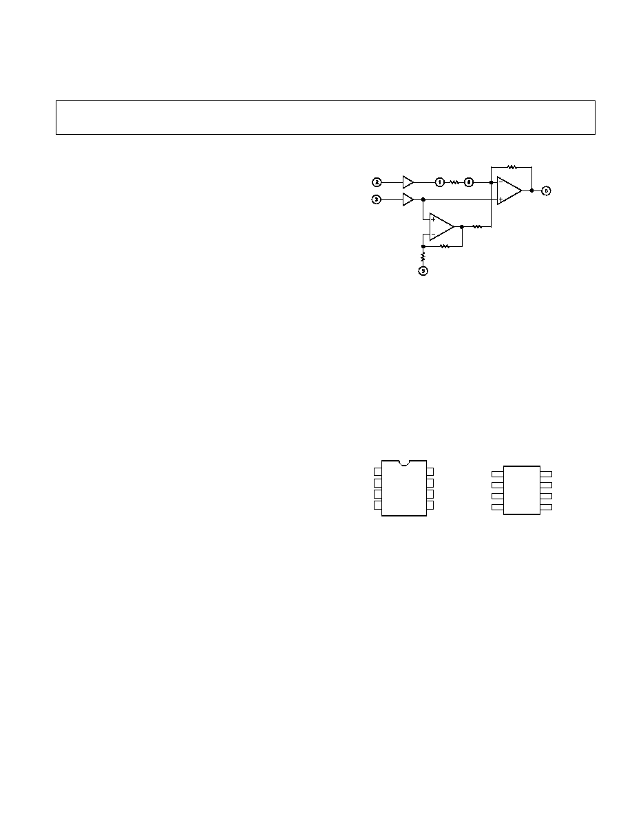
AMP04*
FUNCTIONAL BLOCK DIAGRAM
IN()
IN(+)
INPUT BUFFERS
REF
100k
11k
11k
R
GAIN
V
OUT
100k
FEATURES
Single Supply Operation
Low Supply Current: 700 A Max
Wide Gain Range: 1 to 1000
Low Offset Voltage: 150 V Max
Zero-In/Zero-Out
Single-Resistor Gain Set
8-Lead Mini-DIP and SO Packages
APPLICATIONS
Strain Gages
Thermocouples
RTDs
Battery-Powered Equipment
Medical Instrumentation
Data Acquisition Systems
PC-Based Instruments
Portable Instrumentation
Precision Single Supply
Instrumentation Amplifier
GENERAL DESCRIPTION
The AMP04 is a single-supply instrumentation amplifier
designed to work over a +5 volt to
±15 volt supply range. It
offers an excellent combination of accuracy, low power con-
sumption, wide input voltage range, and excellent gain
performance.
Gain is set by a single external resistor and can be from 1 to
1000. Input common-mode voltage range allows the AMP04 to
handle signals with full accuracy from ground to within 1 volt of
the positive supply. And the output can swing to within 1 volt of
the positive supply. Gain bandwidth is over 700 kHz. In addi-
tion to being easy to use, the AMP04 draws only 700
µA of
supply current.
For high resolution data acquisition systems, laser trimming of
low drift thin-film resistors limits the input offset voltage to
under 150
µV, and allows the AMP04 to offer gain nonlinearity
of 0.005% and a gain tempco of 30 ppm/
°C.
A proprietary input structure limits input offset currents to
less than 5 nA with drift of only 8 pA/
°C, allowing direct con-
nection of the AMP04 to high impedance transducers and
other signal sources.
The AMP04 is specified over the extended industrial (40
°C to
+85
°C) temperature range. AMP04s are available in plastic and
ceramic DIP plus SO-8 surface mount packages.
Contact your local sales office for MIL-STD-883 data sheet
and availability.
PIN CONNECTIONS
8-Lead Epoxy DIP
(P Suffix)
8-Lead Narrow-Body SO
(S Suffix)
*Protected by U.S. Patent No. 5,075,633.
1
2
3
4
8
7
6
5
AMP04
R
GAIN
V+
V
OUT
REF
R
GAIN
IN
+IN
V
AMP04
V+
R
GAIN
V
OUT
REF
R
GAIN
IN
+IN
V
One Technology Way, P.O. Box 9106, Norwood, MA 02062-9106, U.S.A.
Tel: 781/329-4700
World Wide Web Site: http://www.analog.com
Fax: 781/326-8703
© Analog Devices, Inc., 2000
AMP04SPECIFICATIONS
ELECTRICAL CHARACTERISTICS
AMP04E
AMP04F
Parameter
Symbol
Conditions
Min
Typ
Max
Min
Typ
Max
Unit
OFFSET VOLTAGE
Input Offset Voltage
V
IOS
30
150
300
µV
40
°C T
A
+85°C
300
600
µV
Input Offset Voltage Drift
TCV
IOS
3
6
µV/°C
Output Offset Voltage
V
OOS
0.5
1.5
3
mV
40
°C T
A
+85°C
3
6
mV
Output Offset Voltage Drift
TCV
OOS
30
50
µV/°C
INPUT CURRENT
Input Bias Current
I
B
22
30
40
nA
40
°C T
A
+85°C
50
60
nA
Input Bias Current Drift
TCI
B
65
65
pA/
°C
Input Offset Current
I
OS
1
5
10
nA
40
°C T
A
+85°C
10
15
nA
Input Offset Current Drift
TCI
OS
8
8
pA/
°C
INPUT
Common-Mode Input Resistance
4
4
G
Differential Input Resistance
4
4
G
Input Voltage Range
V
IN
0
3.0
0
3.0
V
Common-Mode Rejection
CMR
0 V
V
CM
3.0 V
G = 1
60
80
55
dB
G = 10
80
100
75
dB
G = 100
90
105
80
dB
G = 1000
90
105
80
dB
Common-Mode Rejection
CMR
0 V
V
CM
2.5 V
40
°C T
A
+85°C
G = 1
55
50
dB
G = 10
75
70
dB
G = 100
85
75
dB
G = 1000
85
75
dB
Power Supply Rejection
PSRR
4.0 V
V
S
12 V
40
°C T
A
+85°C
G = 1
95
85
dB
G = 10
105
95
dB
G = 100
105
95
dB
G = 1000
105
95
dB
GAIN (G = 100 K/R
GAIN
)
Gain Equation Accuracy
G = 1 to 100
0.2
0.5
0.75
%
G = 1 to 100
40
°C T
A
+85°C
0.8
1.0
%
G = 1000
0.4
0.75
%
Gain Range
G
1
1000
1
1000
V/V
Nonlinearity
G = 1, R
L
= 5 k
0.005
%
G = 10, R
L
= 5 k
0.015
%
G = 100, R
L
= 5 k
0.025
%
Gain Temperature Coefficient
G/T
30
50
ppm/
°C
OUTPUT
Output Voltage Swing High
V
OH
R
L
= 2 k
4.0
4.2
4.0
V
R
L
= 2 k
40
°C T
A
+85°C
3.8
3.8
V
Output Voltage Swing Low
V
OL
R
L
= 2 k
40
°C T
A
+85°C
2.0
2.5
mV
Output Current Limit
Sink
30
30
mA
Source
15
15
mA
REV. B
2
(V
S
= 5 V, V
CM
= 2.5 V, T
A
= 25 C unless otherwise noted)
AMP04
REV. B
3
AMP04E
AMP04F
Parameter
Symbol
Conditions
Min
Typ
Max
Min
Typ
Max
Unit
NOISE
Noise Voltage Density, RTI
e
N
f = 1 kHz, G = 1
270
270
nV/
Hz
f = 1 kHz, G = 10
45
45
nV/
Hz
f = 100 Hz, G = 100
30
30
nV/
Hz
f = 100 Hz, G = 1000
25
25
nV/
Hz
Noise Current Density, RTI
i
N
f = 100 Hz, G = 100
4
4
pA/
Hz
Input Noise Voltage
e
N
p-p
0.1 Hz to 10 Hz, G = 1
7
7
µV p-p
0.1 Hz to 10 Hz, G = 10
1.5
1.5
µV p-p
0.1 Hz to 10 Hz, G = 100
0.7
0.7
µV p-p
DYNAMIC RESPONSE
Small Signal Bandwidth
BW
G = 1, 3 dB
300
300
kHz
POWER SUPPLY
Supply Current
I
SY
550
700
700
µA
40
°C T
A
+85°C
850
850
µA
Specifications subject to change without notice.
ELECTRICAL CHARACTERISTICS
AMP04E
AMP04F
Parameter
Symbol
Conditions
Min
Typ
Max
Min
Typ
Max
Unit
OFFSET VOLTAGE
Input Offset Voltage
V
IOS
80
400
600
µV
40
°C T
A
+85°C
600
900
µV
Input Offset Voltage Drift
TCV
IOS
3
6
µV/°C
Output Offset Voltage
V
OOS
1
3
6
mV
40
°C T
A
+85°C
6
9
mV
Output Offset Voltage Drift
TCV
OOS
30
50
µV/°C
INPUT CURRENT
Input Bias Current
I
B
17
30
40
nA
40
°C T
A
+85°C
50
60
nA
Input Bias Current Drift
TCI
B
65
65
pA/
°C
Input Offset Current
I
OS
2
5
10
nA
40
°C T
A
+85°C
15
20
nA
Input Offset Current Drift
TCI
OS
28
28
pA/
°C
INPUT
Common-Mode Input Resistance
4
4
G
Differential Input Resistance
4
4
G
Input Voltage Range
V
IN
12
+12
12
+12
V
Common-Mode Rejection
CMR
12 V
V
CM
+12 V
G = 1
60
80
55
dB
G = 10
80
100
75
dB
G = 100
90
105
80
dB
G = 1000
90
105
80
dB
Common-Mode Rejection
CMR
11 V
V
CM
+11 V
40
°C T
A
+85°C
G = 1
55
50
dB
G = 10
75
70
dB
G = 100
85
75
dB
G = 1000
85
75
dB
Power Supply Rejection
PSRR
±2.5 V V
S
±18 V
40
°C T
A
+85°C
G = 1
75
70
dB
G = 10
90
80
dB
G = 100
95
85
dB
G = 1000
95
85
dB
(V
S
= 15 V, V
CM
= 0 V, T
A
= 25 C unless otherwise noted)
AMP04
REV. B
4
AMP04E
AMP04F
Parameter
Symbol
Conditions
Min
Typ
Max
Min
Typ
Max
Unit
GAIN (G = 100 K/R
GAIN
)
Gain Equation Accuracy
G = 1 to 100
0.2
0.5
0.75
%
G = 1000
0.4
0.75
%
G = 1 to 100
40
°C T
A
+85°C
0.8
1.0
%
Gain Range
G
1
1000
1
1000
V/V
Nonlinearity
G = 1, R
L
= 5 k
0.005
0.005
%
G = 10, R
L
= 5 k
0.015
0.015
%
G = 100, R
L
= 5 k
0.025
0.025
%
Gain Temperature Coefficient
G/T
30
50
ppm/
°C
OUTPUT
Output Voltage Swing High
V
OH
R
L
= 2 k
13
13.4
13
V
R
L
= 2 k
40
°C T
A
+85°C
12.5
12.5
V
Output Voltage Swing Low
V
OL
R
L
= 2 k
40
°C T
A
+85°C
14.5
14.5 V
Output Current Limit
Sink
30
30
mA
Source
15
15
mA
NOISE
Noise Voltage Density, RTI
e
N
f = 1 kHz, G = 1
270
270
nV/
Hz
f = 1 kHz, G = 10
45
45
nV/
Hz
f = 100 Hz, G = 100
30
30
nV/
Hz
f = 100 Hz, G = 1000
25
25
nV/
Hz
Noise Current Density, RTI
i
N
f = 100 Hz, G = 100
4
4
pA/
Hz
Input Noise Voltage
e
N
p-p
0.1 Hz to 10 Hz, G = 1
5
5
µV p-p
0.1 Hz to 10 Hz, G = 10
1
1
µV p-p
0.1 Hz to 10 Hz, G = 100
0.5
0.5
µV p-p
DYNAMIC RESPONSE
Small Signal Bandwidth
BW
G = 1, 3 dB
700
700
kHz
POWER SUPPLY
Supply Current
I
SY
750
900
900
µA
40
°C T
A
+85°C
1100
1100
µA
Specifications subject to change without notice.
WAFER TEST LIMITS
Parameter
Symbol
Conditions
Limit
Unit
OFFSET VOLTAGE
Input Offset Voltage
V
IOS
300
µV max
Output Offset Voltage
V
OOS
3
mV max
INPUT CURRENT
Input Bias Current
I
B
40
nA max
Input Offset Current
I
OS
10
nA max
INPUT
Common-Mode Rejection
CMR
0 V
V
CM
3.0 V
G = 1
55
dB min
G = 10
75
dB min
G = 100
80
dB min
G = 1000
80
dB min
Common-Mode Rejection
CMR
V
S
=
±15 V, 12 V V
CM
+12 V
G = 1
55
dB min
G = 10
75
dB min
G = 100
80
dB min
(V
S
= 5 V, V
CM
= 2.5 V, T
A
= 25 C unless otherwise noted)
AMP04
REV. B
5
Parameter
Symbol
Conditions
Limit
Unit
G = 1000
80
dB min
Power Supply Rejection
PSRR
4.0 V
V
S
12 V
G = 1
85
dB min
G = 10
95
dB min
G = 100
95
dB min
G = 1000
95
dB min
GAIN (G = 100 K/R
GAIN
)
Gain Equation Accuracy
G = 1 to 100
0.75
% max
OUTPUT
Output Voltage Swing High
V
OH
R
L
= 2 k
4.0
V min
Output Voltage Swing Low
V
OL
R
L
= 2 k
2.5
mV max
POWER SUPPLY
Supply Current
I
SY
V
S
=
±15
900
µA max
700
µA max
NOTE
Electrical tests and wafer probe to the limits shown. Due to variations in assembly methods and normal yield loss, yield after packaging is not guaranteed for standard
product dice. Consult factory to negotiate specifications based on dice lot qualifications through sample lot assembly and testing.
ABSOLUTE MAXIMUM RATINGS
1
Supply Voltage . . . . . . . . . . . . . . . . . . . . . . . . . . . . . . . . .
±18 V
Common-Mode Input Voltage
2
. . . . . . . . . . . . . . . . . . .
±18 V
Differential Input Voltage . . . . . . . . . . . . . . . . . . . . . . . . . 36 V
Output Short-Circuit Duration to GND . . . . . . . . . . Indefinite
Storage Temperature Range
Z Package . . . . . . . . . . . . . . . . . . . . . . . . . . 65
°C to +175°C
P, S Package . . . . . . . . . . . . . . . . . . . . . . . . 65
°C to +150°C
Operating Temperature Range
AMP04A . . . . . . . . . . . . . . . . . . . . . . . . . . 55
°C to +125°C
AMP04E, F . . . . . . . . . . . . . . . . . . . . . . . . . 40
°C to +85°C
Junction Temperature Range
Z Package . . . . . . . . . . . . . . . . . . . . . . . . . . 65
°C to +175°C
P, S Package . . . . . . . . . . . . . . . . . . . . . . . . 65
°C to +150°C
Lead Temperature Range (Soldering, 60 sec) . . . . . . . . 300
°C
Package Type
JA
3
JC
Unit
8-Lead Cerdip (Z)
148
16
°C/W
8-Lead Plastic DIP (P)
103
43
°C/W
8-Lead SOIC (S)
158
43
°C/W
NOTES
1
Absolute maximum ratings apply to both DICE and packaged parts, unless
otherwise noted.
2
For supply voltages less than
± 18 V, the absolute maximum input voltage is
equal to the supply voltage.
3
JA
is specified for the worst case conditions, i.e.,
JA
is specified for device in
socket for cerdip, P-DIP, and LCC packages;
JA
is specified for device
soldered in circuit board for SOIC package.
ORDERING GUIDE
Temperature
V
OS
@ 5 V
Package
Package
Model
Range
T
A
= 25 C
Description
Option
AMP04EP
XIND
150
µV
Plastic DIP
N-8
AMP04ES
XIND
150
µV
SOIC
SO-8
AMP04ES-REEL7
XIND
150
µV
SOIC
SO-8
AMP04FP
XIND
300
µV
Plastic DIP
N-8
AMP04FS
XIND
300
µV
SOIC
SO-8
AMP04FS-REEL
XIND
150
µV
SOIC
SO-8
AMP04FS-REEL7
XIND
150
µV
SOIC
SO-8
AMP04GBC
25
°C
300
µV
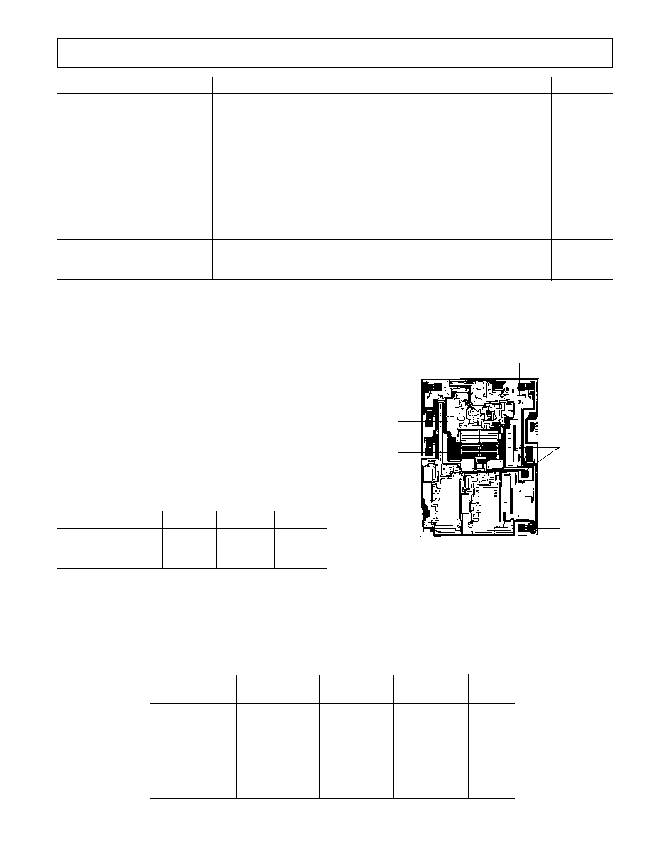
DICE CHARACTERISTICS
R
GAIN
1
R
GAIN
8
7 V+
6 V
OUT
5 REF
IN 2
+IN 3
V 4
AMP04 Die Size 0.075
× 0.99 inch, 7,425 sq. mils.
Substrate (Die Backside) Is Connected to V+.
Transistor Count, 81.