 | ÐлекÑÑоннÑй компоненÑ: AND8020D | СкаÑаÑÑ:  PDF PDF  ZIP ZIP |
Äîêóìåíòàöèÿ è îïèñàíèÿ www.docs.chipfind.ru
©
Semiconductor Components Industries, LLC, 2004
July, 2004 - Rev. 5
1
Publication Order Number:
AND8020/D
AND8020/D
Termination of ECL
Logic Devices with
EF (Emitter Follower)
OUTPUT Structure
Prepared by: Paul Shockman
ON Semiconductor Logic Applications Engineering
CONTENTS OF APPLICATION NOTE
Introduction - DC Termination Analysis
Vt
R
t
R
t
R
t
R
t
R
t
R
t
Vt1
Vt2
External
Internal
Near (Standard Pair)
Far (Standard Pair)
Far (Standard Pair)
V
EE
R
t
R
t
R
t
R
t
R
t
Vt1
Vt2
V
EE
V
to
(Open)
V
EE
(Shorted)
V
TT
Near (Standard Pair)
V
TT
V
TT
R
E
V
EE
Section 2. Parallel Termination - External and Internal
Section 1. Unterminated Lines
R
R
R
R
Section 3. Thevenin Equivalent/Parallel Termination
R
R
Section 4. Series (Back) Termination
V
BB
V
BB
Driver
Receiver
*All Media
*
*
D1
D2
D1
D2
Section 5. Diode Termination
R
R
R
R
R
V
CC
V
BB
Section 6. Capacitive Coupling
R
E
R
E
R
E
R
E
R
E
R
E
R
E
R
E
APPLICATION NOTE
http://onsemi.com
AND8020/D
http://onsemi.com
2
INTRODUCTION
Static DC Termination Analysis
A standard Emitter Coupled Logic (ECL) output driver
typically uses a current switching differential with an emitter
follower for level shifting the output and the internal CML
levels to familiar ECL levels. This output driver architecture
presents about 6-8
W internal impedance in both LOW and
HIGH states when properly current biased. This results in a
typical V
PP
signal of 800 mV
PP
(measured single-endedly on
each line) swinging around a DC voltage point of
V
CC
-
1.3
V when properly terminated and operating
correctly as shown in Figure 1.
Q
V
EE
V
CC
D
V
CC
V
EE
Driver
Receiver
8
W
Internal Output
Impedance
V
EE
Figure 1. Typical ECL Output with Emitter Follower Output Structure,
Typical Termination, and Typical ECL Input Interconnect
Q
D
R
E
R
E
For proper static and dynamic operation, the output
emitter follower transistor must remain in the active region
of operation which requires an external resistive path be
provided from the output pin to a voltage more negative than
worst case V
OL
, such as V
EE
. The resistor, R
E
, is considered
a current bias for the Emitter Follower output structure.
When properly terminated and current biased (loaded),
the outputs will generate both: (1) static state voltage levels
V
OL
(LOW) or V
OH
(HIGH) and (2) a dynamic transition
edge (tr or tf) between state levels.
Static State Voltage Levels
Figure 2 illustrates the typical relationship of static signal
levels and dynamic transition edges between an Output
Driver Signal and a Receiver Input Signal. Both outputs of
a differential driver should always be terminated and loaded
as identically as possible to preserve minimum skew and
jitter operation of the device.
V
IH
V
OH
V
IL
V
CC
V
OL
V
EE
Figure 2. State Levels V
OH
, V
OL
,
and Dynamic Transitions at Q or Q and D or D
V
CC
-1.3 V
tr
tf
V
IH
V
OH
V
IL
V
CC
V
OL
V
EE
V
CC
-1.3 V
tr
tf
Output
Driver
Signal
Input
Receiver
Signal
AND8020/D
http://onsemi.com
3
Output Open, Short, and Safe DC Current
Left open, an output will only swing a few millivolts due
to parasitic "minimum current" leakage paths.
Shorted to V
EE
, a maximum current will develop, limited
only by the output transistor 8
W impedance, and may cause
damage to the output. Worst case short circuit current risks
destruction of the devices.
ISC
+
VOH
RINT
+
4 V
8
W
= 500 mA!
(eq. 1)
Where:
V
OH
= 4.0 V
V
CC
= 5.0 V
V
EE
= 0.0 V
R
int
= 8
W
The continuous safe output current, I
out
(continuous),
maximum limit is 50 mA under all spec operating
conditions. The continuous safe repetitive surge, I
out
(surge), maximum current limit is 100 mA for
10 milliseconds per second duty cycle, provided the device's
total thermal limits are observed. Output current polarity
will always be sinking into the termination scheme during
proper operation.
Static Analysis of Termination Resistor R
E
The output continuous safe current limit, I
out
(cont),
determines R
E
minimum DC termination scheme resistance
to V
EE
although this will not provide a practical AC signal
termination as shown in Table A: Minimum R
E
Values.
RE
+
VOH
I max
(eq. 2)
Table A. Minimum R
E
Values
Line
V
OH
R
E
(min)
PECL
4.0 V
80
W
LVPECL
2.4 V
48
W
LVEP PECL
1.6 V
32
W
A DC terminating resistor minimum, R
E
(min), of 80
W,
while sufficiently limiting the output load current to V
EE
,
may generate insufficient PECL output LOW and HIGH
state transitions.
The R
E
maximum is effectively determined by the
application load capacitance, C
L
, since an RC network is
formed by R
E
and C
L
which limits the signal fall time,
discharging the line to the LOW state voltage level. A
sufficiently high value R
E
or C
L
can cause the signal fall
time to the V
OL
level to violate specification limits.
Designed R
E
or C
L
values may selectively eliminate
undesirable noise.
Dynamic Analysis of Termination Resistor R
E
The dynamic function of the termination resistor, R
E
is to
develop the voltage change,
DV, during a high-to-low or
low-to-high transition and present this to the transmission
medium such as coax, twisted pair, microstrip or stripline.
The
DV signal propagates to the receiver and is either
reflected, dissipated, or a combination.
Since the reflection coefficient at the load is of opposite
polarity to that of the source, a reflection will travel back and
forth over the transmission changing polarity after each
reflection until critically damped by line impedance. Thus,
steps may appear in the signal
DV at the receiving gate input
due to impedance mismatch and consequent partial
reflections.
When R
E
is too large, steps appear in the trailing edge of
the propagating signal,
DV, at the input to the receiving gate,
slowing the edge speed and increasing the net propagation
delay. A reasonable negative-going signal swing at the input
of the receiving gate results when the value of R
E
is selected
to produce an initial step of 75% of the expected
DV, or a
600 mV step for an 800 mV signal at the driving gate. For
a RSECL expected
DV swing of 400, a 300 mV initial step
is desired. Hence for a 600 mV initial step:
( VOH
*
VEE )
( Rt
)
Z0 )
* Z0
y
0.6
I(init) * Z0
u
0.6
(eq. 3)
The value for R
E
is found in Table B: Recommended
Values of R
E
in Dynamic Functional Application. This table
lists recommended R
E
values for the various ECL devices by
Family Series according to the equation above. The table
assumes operation with various data sheet V
OH
values and
various V
CC
values driving a Z
0
= 50
W line. Lowering the
value of R
E
will increase the voltage change,
DV, launched
into the transmission media. Raising the value of R
E
will
decrease the voltage change,
DV, launched into the
transmission media.
Table B. Recommended Nominal Values of R
E
in
Dynamic Functional Application
Series
|V
CC
-V
EE
|
R
E
(
W)
NB
2.5
140
NB
3.3
250
10/100LVEP
2.5
50
10/100EP, 100LVEL
3.3
120
10/100EL, 10/100E
5.0
235
AND8020/D
http://onsemi.com
4
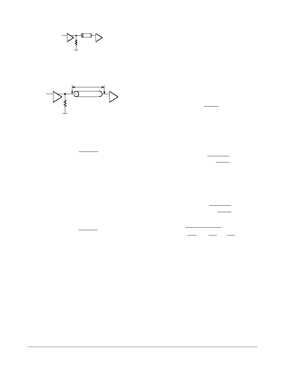
SECTION 1. UNTERMINATED LINES
R
From transmission line theory, when the driver R
E
develops a
DV swing, the signal propagates from point A
arriving at point B at time Td later as shown in Figure 3. This
configuration is also referred to as a stub or an open line.
Figure 3. Unterminated Transmission Line Stub
V
EE
T-Line Z
0
A
B
Td
R
E
At point B, the signal is reflected as a function of
ò
L
. If the
input impedance of the receiving gate is large relative to the
line characteristic impedance, according to Equation 4:
ò
L
+
(RL
*
Z0)
(RL
)
Z0)
(eq. 4)
Where:
ò
L
= Load Reflection Coefficient
R
L
= Load Impedance
Z
0
= Line Characteristic Impedance
A large positive reflection occurs resulting in overshoot.
The reflected signal reaches point A at time 2Td , and a large
negative reflection results because the output impedance of
the driver gate is much less than the line characteristic
impedance (i.e. R
O
<< Z
0
).
When the reflected signal arrives at the source it is
reflected back toward the load with a magnitude dictated by
the source reflection coefficient:
ò
S
+
(Rs
*
Z0)
(Rs
)
Z0)
(eq. 5)
Where:
ò
S
= Source Reflection Coefficient
R
L
= Source Impedance
Z
0
= Line Characteristic Impedance
The reflected signal continues to be reflected by the source
and load impedances and is attenuated with each passage over
the transmission line. The output response appears as a
damped oscillation asymptotically approaching a steady state
value. This phenomena is often referred to as "ringing."
The importance of minimizing the reflected signals lies in
their adverse affect on noise margin and the potential for
driving the input transistors of the succeeding stage into
saturation. Both of these phenomena can lead to less than
ideal system performance. To maximize signal integrity on
transmission lines, four basic techniques are available:
1. Minimizing Interconnect Line Lengths (Section 1)
2. Parallel Termination (Sections 2 and 3)
3. Series Termination (Section 4)
4. Diode Termination (Section 5)
Interconnect Line Lengths
The output signal Waveform rise (tr) and fall (tf) time are
measured from the 20% and 80% levels of the static signal
levels. This edge rate represents the waveforms highest
harmonic and determines the maximum unterminated open
line trace length, L
max
, permissible without sustaining
signal reflections.
The impetus in restricting interconnect lengths, L, is to
mitigate the effects of overshoot and undershoot. A handy
rule of thumb is that the undershoot can be limited to less
than 15% of the logic swing if the two way line delay is less
than the rise time of the pulse. With an undershoot of <15%,
the physics of the situation will result in an overshoot which
will not cause saturation problems at the receiving input.
Thus, the maximum line length can be determined:
L max
t
tr
2 * Tpd
(eq. 6)
Where:
L
max
= Maximum Open Line Length
t
r
= Signal Rise Time
T
pd
= Length Pulse Delay per Unit Length
Further, the propagation delay increases with gate
loading; thus, the effective delay per unit length (T
pdEff
) is
given as:
TpdEff
+
Tpd
1
)
CD
L * CO
(eq. 7)
Where:
T
pd
= Length Pulse Delay per Unit Length
C
D
= Distributed Capacitance
C
O
= Capacitance per Unit Length (Foot)
L = Line Length
Using the effective delay per unit length, Tpd
Eff,
yields:
tr
y
(2) (L) (Tpd )
1
)
CD
L * CO
(eq. 8)
Solving for L
max
line length produces:
L max
+
0.5
CD
CO
2
)
tr
tpd
2
*
CD
CO
(eq. 9)
Where:
L
max
= Line Length Maximum
C
D
= Distributed Capacitance
C
O
= Capacitance per Unit Length (Foot)
T
pd
= Length Pulse Delay per Unit Length
Assuming a worst case capacitance of 2 pF and a rise time
of 100 ps for EP gives a value of 0.03 inch for the maximum
open line length. Maximum open line lengths derived from
SPICE simulations for single and double gate loads, a
maximum overshoot of 40% and undershoot of 20% was
assumed. The simulation results indicate that for a 50
W line,
a stub length of
x 0.03 inches will limit the overshoot to less
than 40%, and the undershoot to within 20% of the logic
swing. Signal traces will most assuredly be larger than
0.03 inch for most practical applications.
Therefore, it will be necessary to use controlled
impedance environments for EP devices in general and
devices with faster edges.
AND8020/D
http://onsemi.com
5
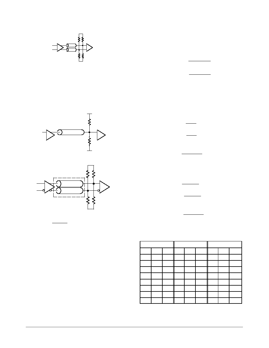
TERMINATION OF ECL LOGIC DEVICES
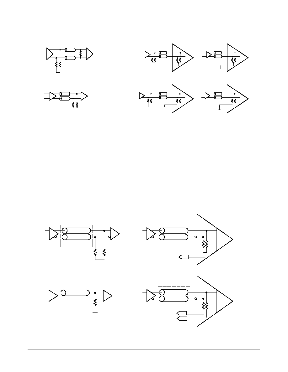
SECTION 2. PARALLEL TERMINATION - EXTERNAL AND INTERNAL
R
t
R
t
External
Internal
Near (Standard Pair)
Far (Standard Pair)
Near (Standard Pair)
Far (Standard Pair)
V
EE
R
t
V
TT
Vt
R
t
R
t
R
t
R
t
Vt1
Vt2
R
t
R
t
R
t
R
t
Vt1
Vt2
V
EE
V
to
(Open)
V
EE
(Shorted)
V
TT
V
TT
R
E
R
E
R
E
R
E
R
E
R
E
Parallel termination advantages:
·
Method of choice for best circuit performance
·
Particularly excellent for driving distributed loads
·
Undistorted waveform along the full length of the line
·
Decreased power consumption.
Far DC Current Return - V
TT
A parallel terminated line is one in which the receiving end
is signal terminated internally or externally (usually to a
voltage V
TT
) through a resistor (R
t
) with a value equal to the
line characteristic impedance (Figure 4). This line also carries
the biasing current for the drivers output far from the driver.
Output current and power dissipation is decreased due to use
of a V
TT
termination supply. The V
TT
supply must sustain the
emitter follower output transistor in its active operating region
under all operating conditions. A minimum continuous current
occurs for the most negative V
OL
, therefore the V
TT
supply
must remain more negative than the worst case V
OLmin
and
always sink current.
Standard V
TT
is 2.0 V below V
CC
supply. A parallel
resistor, R
t
, matching the controlled impedance transmission
line, Z
0
, connects the signal to the V
TT
supply. The Parallel
Termination to V
TT
is shown in Figure 4. The termination
resistors may be internal or external and either ganged into a
Combo pin or offered as Singulated pins. Some devices may
have each internal resistors independently pinned out,
allowing further termination versatility.
Figure 4. Parallel Termination to V
TT
- Differential and Single-Ended with Combo or Singulated Vt Pins (Far Return)
V
TT
R
t
= Z
0
V
TT
=
V
CC
-2.0 V
T-Line Z
0
V
TT
(*or twisted pair)
Driver
Receiver
*T-Line Z
0
*T-Line Z
0
V
TT
R
R
(*or twisted pair)
Driver
Receiver
*T-Line Z
0
*T-Line Z
0
Vt
Driver
Receiver
External (Far, Diff.)
Internal Termination Combo Pin (Far, Diff.)
V
TT
R
R
(*or twisted pair)
Driver
Receiver
*T-Line Z
0
*T-Line Z
0
Vt1
Internal Termination Singulated Pins (Far, Diff.)
R
t
R
t
R
t
Vt2
External (Far, S.E.)
AND8020/D
http://onsemi.com
6
Internal Termination Resistors
Internal termination conveniently uses 50
W values for R
t
,
with the most popular being Z
0
. Note the internal termination
allows the Combo Pin node, V
t
, from the internal resistors to
be connected to an external V
TT
supply, typically at
V
CC
- 2.0 V, as shown in Figure 5. Alternatively, this Combo
Pin may be pulled to V
EE
through an external resistor to form
a "Y" type termination variant, as shown in Figure 5. See the
"Y Variance" topic and the "Y Term Table" for R
t3
resistor
values.
Figure 5. Combo Pin V
TT
or "Y" Connection with
Internal Parallel Termination
V
TT
R
R
(*or twisted pair)
Driver
Receiver
*T-Line Z
0
*T-Line Z
0
V
TT
Connection
V
EE
R
R
(*or twisted pair)
Driver
Receiver
*T-Line Z
0
*T-Line Z
0
Y Connection
R
t3
A.
B.
Example Calculations
Ideally, V
TT
supply tracks 1:1 with V
CC
; however, supply
tolerances need to be considered. Assume for instance a
MC10EP16, +85
°
C, nominal +3.3 V
CC
, terminated 50
W (R
t
)
to V
TT
, where V
TT
is V
CC
- 2.0 V, or 1.3 V:
IOHmax of (VCC )
*
0.885 V
IOLmin of (VCC )
*
1.685 V
resulting in the nominal case:
IOHmax
+
(VOHmax
*
VTT )
Rt
(3.3
*
0.885)
*
1.3
50
+
22.3 mA
IOLmin
+
(VOLmin
*
VTT )
Rt
(3.3
*
1.685)
*
1.3
50
+
6.3 mA
If +5% tolerances are assumed, two worst case conditions result.
Case #1: V
CC
min = V
CC
- 5%, V
TT
max = V
TT
+ 5%
((3.135
*
0.885)
*
1.365)
50
+
17.7 mA
IOHmax
+
(VOHmax
*
VTT)
Rt
IOLmin
+
(VOLmin
*
VTT)
Rt
((3.135
*
1.685)
*
1.365)
50
+
1.7 mA
Case #2: V
CCmin
+ 5%, V
TTmax
- 5%
((3.465
*
0.885)
*
1.235)
50
+
26.9 mA
IOHmax
+
(VOHmax
*
VTT)
Rt
((3.465
*
1.685)
*
1.235)
50
+
1.09 mA
IOLmin
+
(VOLmin
*
VTT)
Rt
Y Variance
The "Y" termination for a differential pair may be
preferred when avoiding the use of a V
TT
supply. The design
is shown in Figure 6 and utilizes the following formulas for
calculating resistor values which are found in the Y Term
Table. The voltage at the Node where R
t1
, R
t2
, and R
t3
connect remains at a static V
TT
voltage of V
CC
- 2.0 V, or
1.3 V.
Rt3
+
Rt1
VTT
*
VEE
VOH
)
VOL
*
2VTT
Rt1
+
Rt2
+
Z0
(eq. 10)
(eq. 11)
VTT
+
Rt3 ( VOH
)
VOL )
)
( Rt1 * VEE )
Rt1
)
2Rt3
(eq. 12)
Figure 6. "Y" Variance
Driver
Receiver
*T-Line Z
0
*T-Line Z
0
V
CC
* or Twisted Pair
R
t1
R
t2
R
t3
C
1
0.1-0.01
m
F
AND8020/D
http://onsemi.com
7
Table C. Y Term Table
|V
CC
-V
EE
| = 5.0 V
|V
CC
-V
EE
| = 3.3 V
|V
CC
-V
EE
| = 2.5 V
Z
0
R
t1
R
t2
R
t3
Z
0
R
t1
R
t2
R
t3
Z
0
R
t1
R
t2
R
t3
50
50
50
112
50
50
50
46
50
50
50
21.2
70
70
70
156
70
70
70
64
70
70
70
29.7
75
75
75
166
75
75
75
68
75
75
75
31.8
80
80
80
179
80
80
80
72
80
80
80
33.9
90
90
90
201
90
90
90
82
90
90
90
38.1
100
100
100
223
100
100
100
91
100
100
100
42.4
120
120
120
268
120
120
120
109
120
120
120
50.8
150
150
150
335
150
150
150
136
150
150
150
63.6
V
EE
R
E
R
E
Figure 7. Standard Pair with External Parallel
R
t
(*or twisted pair)
*T-Line Z
0
*T-Line Z
0
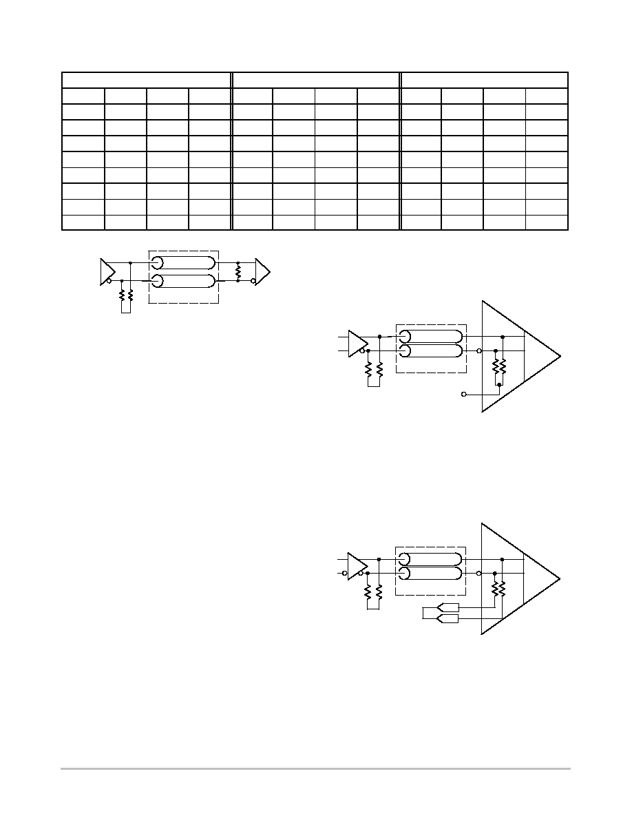
Near DC Current Return - Standard Pair
Termination
The standard pair termination scheme uses a pull-down
resistor, R
E
, located at each driver pin to return the output
transistor bias current near the driver, and an impedance
matching parallel resistor, R
T
, located at the receiver input
pins (see Figure 7, standard pair with external parallel, and
Figure
8, standard pair termination with internal
termination, and Figure 9, standard pair termination with
singulated internal termination resistors). The impedance
matching parallel resistor may be internal or external
depending on the receiver device. If internal to the receiver,
the resistor may be singulated or combined ("combo") for
external pinout.
The diagram of Figure 7 shows a Standard Pair
Termination with an R
E
resistor for DC output current bias
located nearby each driver pin: refer to Table B, for values
of R
E
. The differential transmission line AC impedance
matching resistance, R
t
, is located externally near the
receiver input pins.
As a variation of a Standard Pair Termination, a receiver
may provide the differential transmission line AC
impedance matching resistance, R
t
, internally. This internal
impedance matching termination may be pinned out either
combined into a Combo V
t
pin or each resistor may be
singulated and pinned out, such as V
t1
and V
t2
.
When left open, the Combo Pin still provides a passive
100
W termination across the nearby receiver's differential
signal line pair. This can compliment a pull-down resistor, R
E
,
located on each line of a differential at the driver pins. This is
illustrated in Figure 8.
Figure 8. Standard Pair Termination with
Internal Termination
Open V
t
Pin
R
R
(*or twisted pair)
Driver
Receiver
*T-Line Z
0
*T-Line Z
0
Internal Termination Combo Pin
V
EE
R
E
R
E
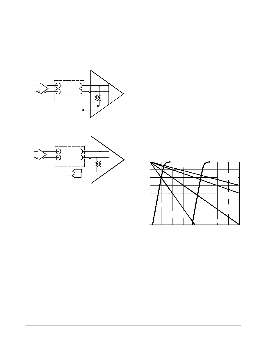
When the Internal Termination resistors are singulated,
the two V
t
pins must be shorted to create the 100
W value as
shown in Figure 9.
Figure 9. Standard Pair Termination with
Singulated Internal Termination Resistors
Internal Termination Singulated Pins
R
R
(*or twisted pair)
Driver
Receiver
*T-Line Z
0
*T-Line Z
0
V
EE
Vt1
Vt2
Shorted
R
E
R
E
AND8020/D
http://onsemi.com
8
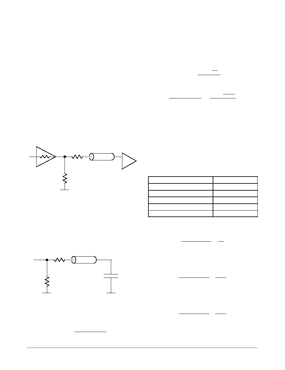
Internal 100
W
Termination (LVDS)
For some technologies, such as LVDS, this passive 100
W
internal termination can provide sufficient termination for the
driver as shown in Figure 10. Devices with a Combo Pin will
require this pin to remain open, while devices with singulated
internal resistors require the two pinned out V
t
nodes for a
differential pair to be shorted together to provide the 100
W
termination.
Figure 10. LVDS Interconnect with Internal
Termination
Open V
t
Pin
R
R
(*or twisted pair)
LVDS Driver
Receiver
*T-Line Z
0
*T-Line Z
0
Internal Termination Combo Pin
Internal Termination Singulated Pins
R
R
(*or twisted pair)
LVDS Driver
Receiver
*T-Line Z
0
*T-Line Z
0
Vt1
Vt2
Shorted
Differential ECL outputs can be terminated as independent
complimentary single-ended lines. Both sides of any
differential pair must be terminated as identically as possible
to minimize phase error and pulse width duty cycle skew.
The I
OH
currents in these two cases will vary the DC V
OH
levels by
$40 mV. However in the vast majority of cases, DC
levels are well centered in their specification windows, thus
this variation will simply move the level within the valid
specification window and no loss of worst case noise margin
will be seen.
The I
OL
situation on the other hand does pose a potential
AC problem. In the worst Case #1 I
OLmin
situation, the
output emitter follower could move into the cutoff state
(0 mA). The output emitter followers of ECL devices are
designed to be in the conducting, active region of operation
at all times. When forced into cutoff, the delay of the device
will be increased due to the extra time required to pull the
output emitter follower out of the cutoff state. Again, this
situation will arise only under a number of simultaneous
worst case situations and therefore, is highly unlikely to
occur. But, because of the potential, it should not be
overlooked.
Output Drive Characteristics
Figure 11 shows the nominal output characteristics for
ECL devices operating in negative ECL mode, driving
various load impedances (including the standard 50
W)
returned to a negative two volt supply. The output
resistances, RH (high state output resistance) and RL (low
state output resistance), are obtained from the reciprocal of
the slope at the desired operating point. Many applications
require loads other than 50
W - the resulting V
OH
and V
OL
levels can be estimated using the following technique.
V
OH
-2.0
0
-5
-10
-15
-0.75
-1.0
-1.25
-20
-25
-30
-35
-40
-1.75
-0.5 -0.25
0
OUTPUT VOLTAGE (V)
OUTPUT CURRENT (mA)
SLOPE = 6
W
- 8
W
-1.5
Figure 11. Normal Output Levels Driving Various
Load Impedances
V
OL
T
A
=25
°
C
25
W
to - 2.0 V
50
W
to - 2.0 V
150
W
to - 2.0 V
100
W
to - 2.0 V
AND8020/D
http://onsemi.com
9
SECTION 3. THEVENIN EQUIVALENT PARALLEL TERMINATION
R
R
R
R
Although the single resistor termination to V
TT
conserves
power, it requires an additional supply voltage. An alternate
approach to using a V
TT
power supply is to use a resistor
divider network as shown in Figure 12 to develop a
Thevenin voltage, V
TT
, and provide a parallel impedance
matching AC termination, the Thevenin parallel
termination.
Figure 12. Thevenin Equivalent Parallel Termination
V
EE
T-Line Z
0
Driver
R2
R1
V
CC
Receiver
R2
R2
R1
R1
Driver
Receiver
T-Line Z
0
T-Line Z
0
V
EE
V
CC
or Twisted Pair
VTT
+
VCC
*
2.0V
+
VCC
R2
R1
)
R2
*
*
*
*
*
*
*
(eq. 13)
Differential ECL outputs can be terminated as independent
complimentary single-ended lines. Both sides of a
differential pair must be terminated. Balanced, symmetrical
loading of each line must be preserved.
While a Thevenin Parallel technique dissipates more
termination power, it does not require the additional V
TT
supply. This additional power is consumed entirely in the
external resistor divider network and thus will not change
the current being sourced by the device, hence it does not
alter the IC reliability or lifetime. As with standard parallel
termination, variance of V
TT
and V
CC
supplies must be
considered.
The Thevenin equivalent of the two resistors needs to be
equal to the characteristic impedance of the signal
transmission line. Calculated values for resistors R1 and R2
may be obtained from the following relationships.
R2
+
Z0
VCC
*
VEE
VCC
*
VTT
(eq. 14)
R1
+
R2
VCC
*
VTT
VTT
*
VEE
(eq. 15)
Where:
V
TT
= V
CC
- 2.0 V
Z
0
= Characteristic Impedance of the Signal
Transmission Line
For a typical V
CC
= 5.0 V PECL scheme, where V
EE
=
GND, V
TT
= 3.0 V, and Z
0
= 50
W:
R2
+
50
5
*
0
5
*
3
+
125
W
(eq. 16)
R1
+
125
5
*
3
3
*
0
+
83.3
W
(eq. 17)
and cross-checking for V
TT
:
VTT
+
5
125
125
)
83.3
+
3.0 V
(eq. 18)
VTT
+
VCC
*
2.0 V
+
3.0 V
(eq. 19)
For the typical V
CC
= 3.3 V LVPECL scheme, where
V
EE
= GND, V
TT
= 1.3 V, and Z
0
= 50
W:
R2
+
50
3.3
*
0
3.3
*
1.3
+
82.5
W
(eq. 20)
R1
+
82.5
3.3
*
1.3
1.3
*
0
+
126
W
(eq. 21)
and cross-checking for V
TT
:
VTT
+
3.3
82.5
126
)
82.5
+
1.3 V
(eq. 22)
VTT
+
VCC
*
2.0 V
+
1.3 V
(eq. 23)
Table D. Thevenin Term Table
|V
CC
-V
EE
| = 5.0 V
|V
CC
-V
EE
| = 3.3 V
|V
CC
-V
EE
| = 2.5 V
Z
0
R1
R2
Z
0
R1
R2
Z
0
R1
R2
50
83
125
50
127
83
50
250
62.5
70
117
175
70
178
115
70
350
87.5
75
125
188
75
190
123
75
375
93.8
80
133
200
80
203
132
80
400
100
90
150
225
90
229
149
90
450
112.5
100
167
250
100
253
165
100
500
125.5
120
200
300
120
305
198
120
600
150
150
250
375
150
381
248
150
750
187.5

AND8020/D
http://onsemi.com
10
Because the resistor divider network of R1 and R2 is used
to generate V
TT
, the variation in V
TT
will be intimately tied
to the variation in V
CC
. Differentiating the equation for V
TT
with respect to V
CC
yields:
D
VTT
D
VCC
+
R2
( R1
)
R2 )
D
VCC
(eq. 24)
For the nominal case, this equation reduces to:
D
VTT
+
0.6
D
VCC
(eq. 25)
If
DV
CC
=
$5% = $0.25 V, then DV
TT
=
$0.15 V.
As mentioned previously, the real potential for problems
will be if the V
OL
level can potentially put the output emitter
follower out of the active operating region and into cutoff.
Because of the relationship between the V
CC
and V
TT
levels,
the only cutoff risk condition occurs at V
CCmin
, the lowest
value of V
CC
. Applying the equation for I
OLmin
under this
-5% V
CC
condition yields:
IOLmin
+
( VOLmin
*
VTT )
Rt
(eq. 26)
IOLmin
+
(4.75
*
1.85)
*
2.85
50
+
1.0 mA
(eq. 27)
The results of this cutoff risk analysis show there is no
potential for the output emitter follower to be in cutoff. This
would indicate a Thevenin equivalent termination scheme is
more robust to variation in V
CC
. Since the designer has the
flexibility of choosing the V
TT
level via the selection of the
R1 and R2 resistors, the following procedure can be used.
At -5% minimal variation case for V
CC
:
V
CC
= 4.75 V
V
TT
= V
CC
- 2.0 V = 2.75 V
R2 = 119
W
R1 = 86
W
Thus:
I
OHmax
= 23 mA
I
OLmin
= 3.0 mA
At +5% minimal variation case for V
CC
:
V
CC
= 5.25 V
V
TT
= 3.05 V
Thus:
I
OHmax
= 28 mA
I
OLmin
= 5.2 mA
Although the output currents are slightly higher than
nominal, the elimination of emitter follower cutoff risk is
well justified.
When the equivalent termination resistance matches the
line impedance, no reflection occurs because all the energy
in the signal is dissipated by the termination. Hence, in
comparing properly terminated schemes parallel and
Thevenin, a primary consideration is the power supply
requirements. As mentioned earlier, the parallel V
TT
scheme
requires an extra power supply; however, the Thevenin
termination dissipates 10 times more DC power.
Fortunately, this extra power dissipation cannot be seen on
the die; therefore, either technique results in similar die
junction temperatures.
AND8020/D
http://onsemi.com
11
SECTION 4. SERIES TERMINATION
R
R
R
R
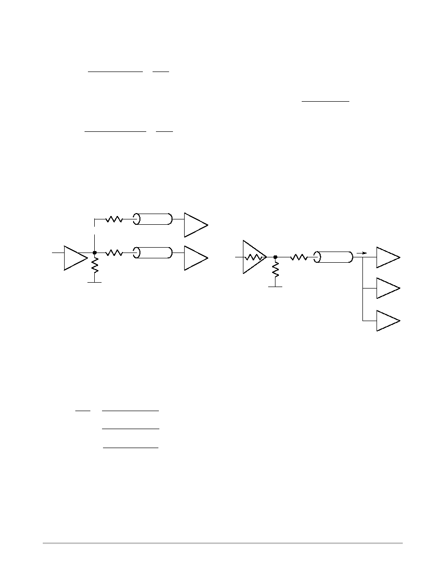
Series Damping is a technique in which a termination
resistance is placed between the driver and the transmission
line with no termination resistance placed at the receiving
end of the line (Figure 13).
*T-Line Z
0
*T-Line Z
0
*T-Line Z
0
Driver
R
t
V
EE
R
S
R
S
* Optional
Receiver
Driver
V
EE
R
S
* Optional
Receiver
Figure 13. Series Termination
or Twisted Pair
R
t
R
t
Differential ECL outputs can be terminated as
independent complimentary single-ended lines. Both sides
of any differential pair must be terminated as identically as
possible to minimize phase error and pulse width duty cycle
skew.
Series Termination is a special case of series damping in
which the sum of the termination resistor (R
S
) and the output
impedance of the Driver gate (R
O
) is equal to the line
characteristic impedance (Figure 14).
RS
)
RO
+
Z0
(eq. 28)
Where:
R
S
= Series Termination Resistor
R
O
= Output Impedance
Z
0
= Line Characteristic Impedance
*T-Line Z
0
V
EE
R
S
Receiver
Figure 14. Series Termination
Driver
V
O
A
B
R
O
R
t
Series termination techniques are useful when the
interconnect lengths are long or impedance discontinuities
exist on the line. Additionally, the signal travels down the
line at half amplitude minimizing problems associated with
crosstalk. Unfortunately, a drawback with this technique is
the possibility of a two-step signal appearing when the
driven inputs are far from the end of the transmission line.
To avoid this problem, the distance between the end of the
transmission line and input gates should adhere to the
guidelines specified from the section on unterminated lines.
Series Termination Theory
When the output of the series terminated driver gate
switches levels, this driver output voltage change,
DV
O
, is
impressed on the input to the transmission line (Point A) as
a change in voltage (
DV
A
) and propagates to the Receiver at
the output of the transmission line (Point B) as a change in
voltage (
DV
B
) in Figure 14.
D
VA
+ D
VO *
Z0
RS
)
RO
)
Z0
(eq. 29)
Where:
DV
A
= Input to the Transmission Line Voltage
Change
DV
B
= Receiver Input Voltage Change
DV
O
= Driver Output Voltage Change
Z
0
= Line Characteristic Impedance
R
O
= Output Impedance of the Driver Gate
R
S
= Termination Resistance
Since Z
0
= R
S
+ R
O
, substitution into the above equations
yields:
D
VA
+
D
VO
2
(eq. 30)
AND8020/D
http://onsemi.com
12
From this relationship,
DV
A
=
DV
O
/ 2, an incident wave
of half amplitude propagates down the transmission line. At
the Receivers input Point B, typically high impedance, the
transmission line sees an unterminated open line and the
signal reflection coefficient at the Receiver load is
approximately unity. The reflection causes the voltage to
double at the receiving end. When the reflected wave arrives
back at the source end, its energy is dissipated by the series
resistor. When the sum of the source and series impedance
is equal to the characteristic impedance of the line, no further
reflections occur.
Calculation of R
t
The Emitter Pull-Down Resistor, R
t
, functions to
establish V
OH
and V
OL
levels. Voltage transitions imposed
on R
t
propagate through R
S
and Z
0
to a receiver. Negative
voltage transition are current limited by R
t
, R
S
, and Z
0
when
the driver output switches to the low state. The R
t
value must
maximize the negative voltage transition and prevent the
output transistor from entering the cutoff operating region in
a low state (Figure 15).
*T-Line Z
0
V
EE
R
S
Receiver
Figure 15. Equivalent Circuit for RE Determination
Driver
R
O
R
t
The worst case scenario occurs when the driver output
emitter follower enters into cutoff during a negative going
transition. When this happens, the driver can be considered
opened and, at the instant it opens, the line characteristic
impedance behaves as a linear resistor returned to V
OH
. The
model becomes a simple series resistive network as shown
in Figure 16.
*T-Line Z
0
V
EE
R
S
Figure 16. Equivalent Circuit with Output Cutoff
V
EE
V
OH
R
t
The maximum current, I
max
, occurs at the instant the
switch opens and is calculated by:
I max
+
( VOH
*
VEE )
( Rt
)
RS
)
Z0 )
(eq. 31)
An initial current, I
init
,
must be sufficient to generate a
transient voltage equal to half of the logic swing since the
voltage at the receiver will double due the reflection
coefficient approaching 1.0 for series termination. To
accommodate reflections caused by discontinuities and load
capacitances the transient voltage should be increased by
25%. Thus, I
init
is defined as:
Iinit
+
1.25 *
Vpp
2
Z0
(eq. 32)
To satisfy the initial constraints of I
max
> I
init
:
( VOH
*
VEE )
( Rt
)
RS
)
Z0 )
u
1.25 *
VSWING
2
Z0
(eq. 33)
Solving for R
t
, gives the inequality:
Rt
v
( KZ0 ) Z0
*
RS
(eq. 34)
Where:
Z
0
= Line Characteristic Impedance
R
O
= Output Impedance of the Driver Gate
R
S
= Termination Resistance
KZ
0
= Coefficient to Z
0
For various series, the coefficient to Z
0
, KZ
0
, is presented
in Table E: Coefficient to Z
0
.
Table E. Coefficient to Z
0
Series
KZ
0
10EP
4.0
100LVEL
4.01
10EL
5.99
10E
7.10
100E
6.57
For the 10EP series (LVPECL mode operation),
where V
OH
= 2.4 V, V
SWING
= 0.8 V, and V
EE
= 0.0 V:
(2.4
*
0.0)
(Rt
)
RS
)
Z0)
y
0.5
Z0
* Z0
*
RS
y
Rt
4.0
(eq. 35)
For the 100LVEL series (LVPECL mode operation),
where: V
OH
= 2.345 V, V
SWING
= 0.750 V, V
EE
= 0.0 V:
(2.345
*
0.0)
(Rt
)
RS
)
Z0)
y
0.468
Z0
* Z0
*
RS
y
Rt
4.01
(eq. 36)
For the 10EL series (PECL mode operation),
where: V
OH
= 4.185 V, V
SWING
= 0.958 V, V
EE
= 0.0 V:
(4.185
*
0.0)
(Rt
)
RS
)
Z0)
y
0.599
Z0
* Z0
*
RS
y
Rt
5.99
(eq. 37)
AND8020/D
http://onsemi.com
13
For the 10E series (ECL mode operation),
where: V
OH
= -0.9 V, V
SWING
= 0.85 V, V
EE
= -5.2 V:
(
*
0.9)
*
(
*
5.2)
Rt
)
Rs
)
Z0
y
0.531
Z0
* Z0
*
Rs
y
Rt
7.10
(eq. 38)
For the 100E series (ECL mode operation),
where: V
OH
= -0.955 V, V
SWING
= 0.75 V, V
EE
= -4.5 V:
(
*
0.955)
*
(
*
4.5)
Rt
)
Rs
)
Z0
y
0.468
Z0
* Z0
*
Rs
y
Rt
6.57
(eq. 39)
Parallel Fanout of Series Termination
An extension of the series termination technique, using
parallel fanout, eliminates the problem of lumped loading at
the expense of extra transmission lines (Figure 17).
*T-Line Z
0
R
S
n
Receiver
n
Figure 17. Parallel Fanout Using Series Termination
*T-Line Z
0
R
S
1
Receiver 1
Driver
R
t
V
EE
N number of lines
Figure 17 shows a modification of the series termination
scheme in which several series terminated lines in parallel
fanout are driven using a single ECL gate. The principle
concern when applying this technique is to maintain the
current in the output emitter follower below the maximum
rated value. The value for R
t
can be calculated by viewing
the circuit in terms of conductances.
Goutput
u
G1
)
G2
)
G
n
(eq. 40)
From Table B, for each of the series:
1
( Rt )
y
1
(
* Z01
*
RS1)
KZ
0
)
1
(
* Z02
*
RS2)
KZ
0
)
1
(
* Z0
*
RS)
n
KZ
0
(eq. 41)
Where:
n = Number of Parallel Circuits
When:
Z01
+
Z02
+
Z0 , and RS1
+
RS2
+
RS
n
n
(eq. 42)
Then R
t
is calculated as:
Rt
x
(KZ0 * Z0
*
Rs)
r
n
(eq. 43)
When a single series terminated line is driving more than
a single receiver, the maximum number of loads must be
addressed. The factor limiting the number of loads is the DC
voltage drop across the series termination resistor caused by
the summary input currents I
T
during the receivers quiescent
high state. Noise margin loss, NM
loss
, will probably
determine the acceptable DC voltage drop limit across R
s
.
NMloss
+
IT * ( Rs
+
RO )
(eq. 44)
Where:
I
T
= Sum of IINH Currents
R
O
= Output Impedance of the Driver Gate
R
S
= Termination Resistance
Figure 18. Noise Margin Loss Example
*T-Line Z
0
R
S
Receiver 1
Driver
R
t
V
EE
R
O
Receiver 2
Receiver
N
I
T
For the majority of ECL devices typical maximum value
for quiescent high state input current is 150 uA. Thus, for the
circuit shown in Figure 18, in which three gate loads are
present in a 50
W environment, the loss in high state noise
margin is calculated as:
NMloss
+
3 *
*
150 mA * 50
W + *
22.5 mV
(eq. 45)
This represents a potential shift in the V
OH
level of
-22.5 mV.
AND8020/D
http://onsemi.com
14
SECTION 5. DIODE TERMINATION
V
BB
V
BB
Driver
Receiver
*All Media
*
*
D1
D2
D1
D2
Alternative to the resistor network termination schemes,
a Diode method shown in Figure 19 may afford certain
advantages when a design has the following constraints.
1. Impedance controlled media line is not required
(coax, twisted pair, striplines, etc.)
2. Impedance matched termination network is not
required.
3. Overshoot and Noise need to be clamped to logic
HIGH/LOW levels.
Figure 19. Diode Termination
V
BB
V
BB
Driver
Receiver
*All Media
*
*
D1
D2
D1
D2
V
BB
Driver
Receiver
*All Media
*
D1
D2
D1 and D2 diodes may be an MBD301, MMBD301,
MBD701, MMBD701LT1, or a dual package MMBD452LT1.
Diode forward voltage curves from a data sheet, such as shown
in Figure 20, will determine specific current and voltage
operation range. Frequency limitations may be a consideration
when selecting the diodes. The Silicon Hot-Carrier Schottky
Barrier diode MBD701, for example, displays a forward V
f
of
about 0.55 V and an I
f
of about 11 mA (at 25
°
C) to match a
50
W impedance line. At higher temperatures, the current
decreases.
Figure 20. MMBD701 Diode Forward Voltage
0.1
1.0
10
100
0
0.2
0.4
0.8
1.2
1.6
2.0
I
F
, FOR
W
ARD CURRENT (mA)
V
F
, FORWARD VOLTAGE (V)
T
A
= 85
°
C
T
A
=-40
°
C
T
A
= 25
°
C
AND8020/D
http://onsemi.com
15
SECTION 6. CAPACITIVE COUPLING
R
R
R
R
R
V
CC
V
BB
Although not strictly a termination, AC or capacitive
coupling is often used to provide features in conjunction
with proper termination. Such capabilities as hot swapping
capability, DC isolation to a receiver, and level shifting are
possible with capacitive coupling.
Data stream characteristics may impose restriction on
both termination and capacitive coupling. AC coupled
signals have the line DC blocked and will require a DC
restoration voltage, V
BIAS
, for the receiver input. Data in
unencoded Non-Return-to-Zero (NRZ) format will require
DC restoration prior to AC coupling into a ECL receiver
input.
A sinusoidal waveform clock signal may be cap coupled
for conversion to a square wave with 50% duty cycle and
sharp rise and fall edges.
The capacitor used to couple the signal must have a
impedance rating of < 50
W over the frequency range of the
input signal. Because large capacitors appear somewhat
inductive at high frequencies, it may be necessary to use a
small capacitor in parallel with a larger one to achieve
satisfactory operation.
A coupling capacitor and the signal load impedance form
an RC network which will boundary the duration of a pulse.
Values for the R (load and leakage total resistance) and C
(coupling capacitor) should be selected to provide a time
constant, T
C
, of at least 10x the pulse width. Data streams
may require larger T
C
values to retain logic levels.
Hot Swapping
The desire often arises to remove or install a receiver or
daughter card without powering down the driver or
motherboard. This is termed "Hot Swapping".
Powered Driver and an Unpowered Receiver
Damage Risk
Hot swapping presents a potential risk to an unpowered or
powered down ECL device receiver and driver in either the
Negative or Positive mode when driven by a typical signal
level.
When a receiver PECL receiver V
CC
is off or powered
down, the V
CC
Power Supply typically appears as a low
impedance source at 0.0 V capable of sinking considerable
current. Typical driver signal levels present voltages that
forward bias the input ESD protection diode structure and
the input base collector junction. Potentially lethal current
paths may develop through forwarded junctions to V
CC
.
There is also a risk for a powered down or off NECL or
LVNECL receiver and driver. A V
EE
supply will typically
appear as a low impedance path to 0.0 V (GND). Typical
negative levels present signal voltages that will forward bias
the input ESD protection diode structure and the input base
collector junction to this low impedance path. Potentially
lethal current paths may develop through the forwarded
junctions and V
EE
to 0.0 V.
Powered down receiver risk may be managed in several
ways.
1. Physical Sequencing - the supplies for V
EE
(Ground) and V
CC
(Power) may be physically
connected prior to signal lines by altering the
daughter board edge connection geometry, making
V
EE
and V
CC
connectors protrude and engage or
sequence first. V
EE
connectors could even be
sequenced prior to V
CC
.
This insures the supplies
are powered prior to input signal voltages.
2. Switching - a relay (or analog switch) could be
used to open or close the supply lines insuring the
power supply line is opened when powered off.
3. Cap Coupling - DC isolation of potentially
damaging current.
4. Series R - an additional series impedance matching
resistor, R
S
, will act as power splitter with an
existing parallel termination resistor, R
T
, to
accomplish some current limiting to help manage
the risk. This will also attenuate the amplitude
50%, easily tolerated by most high gain, high input
sensitivity devices.
Using V
BB
Pin for V
BIAS
Some devices provide a convenient V
BB
pin for use as a
VBIAS reference supply to rebias a DC level. A DC rebias
level must be at the common mode voltage of the input
signal to properly preserve a 50% output duty cycle (see
AND8066). A package V
BB
pin may provide an internally
generated DC switching reference voltage for the device
inputs, and is available only to the package input pins. Do not
port one package V
BB
pin directly to another device without
current amplification. When used, decouple V
BB
to V
CC
(or
V
TT
) via a 0.01 to 0.001
mF capacitor to suppress noise
injection. Limit current to less than 0.5 mA (Absolute
Maximum Rating source or sink) as shown in Figure 21.
When not used, V
BB
should be left open.
AND8020/D
http://onsemi.com
16
Figure 21. Differential and Single-Ended AC
Configurations Using V
BB
Reference
V
CC
or
V
TT
V
CC
Rpu 25 k
W
to 100 k
W
Receiver
OUT
OUT
IN
INb
R
t
V
BB
V
TT
1 k
W
* 0.001
m
F
0.001
m
F
V
CC
or
V
TT
V
CC
Rpu 25 k
W
to 100 k
W
Receiver
OUT
OUT
IN
V
BB
V
TT
1 k
W
* 0.001
m
F
0.01 - 0.001
m
F
R
t
R
t
R
t
* High Voltage Cap May Be Needed
0.01 - 0.001
m
F
A. Differential
B. Single-Ended
In Figure 21A, the IN line has a 1 k
W resistor to V
BB
,
presenting a 1 K
W impedance across the differential signal
lines. This assumes the signal impedance matching has been
accomplished prior to the cap coupling, on the driver side of
cap. Locate the coupling capacitor as physically close to the
input pin as possible to minimize the trace length and
diminish potential reflections due to the impedance
mismatch.
If signal impedance matching has not been accomplished
prior to the cap coupling, then a characteristic impedance
resistor, 2Z
0
, would be used across the input lines, on the
receiver side of the cap. The value of the Rpu resistor would
be adjusted to produce an acceptable null signal default
voltage drop.
Auto-Oscillation Suppression with V
BB
If the differential inputs to the AC coupled device are left
open or if the driving signals are lost, both receiver input pin
voltages converge toward the VBIAS reference voltage V
BB
value. Sustained oscillation may autonomously result from
a combination of ambient environmental noise, the device
small signal gain, and feedback from the output to the input
through parasitic capacitive and inductive paths.
As a differential receiver input voltage diverges, the
output responds by transitioning toward a state voltage. A
sufficient voltage
D across the receiver inputs will force the
output to state level. Depending on conditions, about 10 to
50 mV is sufficient to suppress instability oscillation and
force a determined state on the output.
For the configuration using the V
BB
reference, Figure 21,
this input voltage
D may be accomplished by injecting a
minimum current from V
CC
through an external pullup
resistor, Rpu, on ONE input line. The value of Rpu could
range from 25 k
W to 100 kW. As Rpu increases, the phase
error is diminished and the susceptibility to oscillation
increases.
Generally, an internal pull-down resistor ranging in value
from 52 k
W to 75 kW is deployed on an input pin. On some
D-bar (Invert) input pins an additional 36 k
W to 75 kW
resistor is deployed to suppress oscillation by forcing a
determined state on the output under open input or null
voltage conditions. A minimum input voltage
D of 20 to
30 mV may be effective depending on noise, gain, and
layout.
Generating V
BB
for VBIAS
When V
BB
voltages are desired, but not available within
a device, the reference level may be ported from a generator
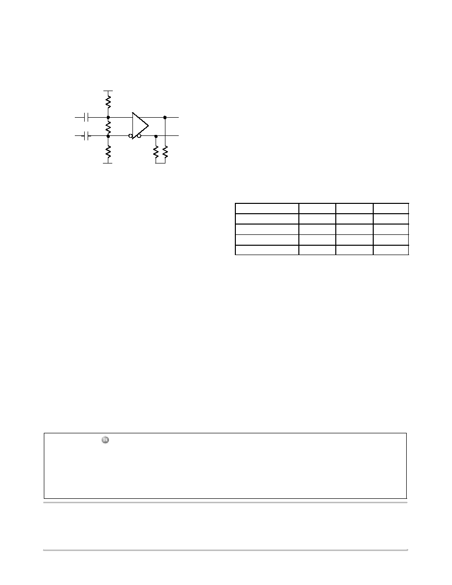
as illustrated in Figure 22. Any of the "16" type buffers are
recommended for use in a high current gain V
BB
Generator
buffer. For example, the E416, EL16, LVEL16, EP16,
LVEP16, EL17, LVEL17, etc. type devices have a V
BB
pin
available for constructing a V
BB
Generator buffer.
Figure 22. V
BB
Voltage Reference Generator
V
BB(out)
16
RT
V
TT
V
CC
or V
TT
V
BB
0.01
m
F
1 K
W
Non-V
BB
Biasing
Alternative to a device supplied V
BB
, any voltage source
may be supplied to bias receiver inputs to provide an
acceptable V
IHCMR
(Voltage Input HIGH Common Mode
Range) DC reference to the receiver (see specific device data
sheet). Signal impedance matching may be accomplished
prior to cap coupling, allowing a wide range values for a
rebiasing resistor network.
AND8020/D
http://onsemi.com
17
When the coupling capacitor is physically located near
enough to the receiver input pins to prohibit reflections on the
connecting trace length or signal impedance matching has
been accomplished prior to cap coupling, then a simple high
value resistor divider network from V
CC
to V
EE
is
recommended as shown in Figure 23. Differential and
Single-Ended AC Configurations Using Non-V
BB
Biasing
(A and B). This network total resistance may be from 1 K
W
to 10 K
W. For 50 W impedance traces, the typical value for the
voltage divider resistors are given in Table F. Typical Rebias
and Impedance Matching Resistor Network Values @
Z
0
= 50. Note the impedance presented to a signal is
u5 KW.
Table F. Typical Rebias and Impedance Matching Resistor Network Values @ Z
0
= 50
Resistor
|V
CC
-V
EE
| = 5.0 V
|V
CC
-V
EE
| = 3.3 V
|V
CC
-V
EE
| = 2.5 V
Units
R1 (R1
)
4
4
4
K
W
R2 (R2
)
6
6
6
K
W
V
rebias
3.3
2.2
1.7
V
When the coupling capacitor is physically located at a
distance from receiver over a trace or cable length capable
of sustaining reflections, a Thevenin parallel network
matching the line of impedance is recommended for their
suppression. This is shown in Figure 23. Differential and
Single-Ended AC Configurations Using Non-V
BB
Biasing
(A and B). The rebias voltage may always be safely set at
V
CC
-1.3. For 50
W impedance traces, the typical value for
the voltage divider resistors are given in Table G. Typical
Rebias and Impedance Matching Resistor Network Values @
Z
0
= 50.
Table G. Typical Rebias and Impedance Matching Resistor Network Values @ Z
0
= 50
Resistor
|V
CC
-V
EE
| = 5.0 V
|V
CC
-V
EE
| = 3.3 V
|V
CC
-V
EE
| = 2.5 V
Units
R1 (R1
)
68
83
96.15
W
R2 (R2
)
192
127
104.16
W
V
rebias
3.7
2.0
1.2
V
Figure 23. Differential and Single-Ended AC
Configurations Using Non-V
BB
Biasing
V
CC
Receiver
OUT
OUTb
IN
INb
R
t
R
t
V
TT
0.001
m
F
0.001
m
F
V
EE
R2
R2
R1
R1
V
CC
Receiver
OUT
OUTb
IN
V
TT
0.001
m
F
V
EE
R2
R2
R1
R1
R
t
R
t
A. Differential
B. Single-Ended
The characterized V
BB
reference voltage bias, VBIAS, is
V
CC
- 1.33 V, but a device is not restricted to this VBIAS
value. The VBIAS range is determined by the Vpp
amplitude and the signal HIGH level, V
IH
. Input HIGH
level, V
IH
, is constrained by the data sheet specification of
common mode range, V
IHCMR
or V
CMR
. Thus, the VBIAS
range is constrained:
VBIAS max
+
VIHCMRmax
*
( 0.5 ) ( Vpp )
VBIAS min
+
VIHCMRmin
*
( 0.5 ) ( Vpp )
A single-ended source into a differential type input signal
amplitude swing, V
pp
, is typically constrained from
V
ppmin
= 300 mV to V
ppmax
= 1000 mV.
An input signal must swing symmetrically above and
below VBIAS to preserve a 50% duty cycle out of the
receiver. Differential signals must have identical crosspoint
voltages to preserve minimum phase error and duty cycle
error. Crosspoint voltages are determined by the matched
precision of the resistor divider network from V
CC
to V
EE
.
Auto-Oscillation Suppression without V
BB
For a configuration without a V
BB
reference pin, such as
illustrated in Figure 23, the resistor network may be
modified to have an input voltage
D of 20 to 30 mV offset
between the input pins. Either a high resistor value divider
or a Thevenin parallel network may be modified to
accomplish this input voltage
D. This is accomplished by
altering the values of R1, R1
, R2, and R2
.
AND8020/D
http://onsemi.com
18
Combining the high impedance and impedance matching
networks results in an input voltage scheme shown in
Figure 24. This creates the proper input voltage
D, VBIAS,
using fewer components.
V
TT
V
CC
Figure 24. VBIAS and Auto-Oscillation Suppression
with Thevenin Parallel Network
R1
Receiver
OUT
OUTb
IN
R
t
R
t
V
EE
0.001
m
F
R
Z
R2
INb
0.001
m
F
For a 3.3 V V
CC
, the values of R1 and R2 provide a
Thevenin parallel network divider voltage with V
IH
in the
V
IHCMR
of the receiver. Current through the divider
develops the default offset across R
z
and can be adjusted as
needed. For example, in Z
0
= 50 traces, a 30 mV default
offset difference will be created if V
CC
= 3.3 V and the DC
bias voltage is 2.0 V (typical V
BB
) when:
R1
+
4.22 k
W
R2
+
6.34 k
W
RZ
+
100
W
The 0.001 coupling cap may need to be adjusted to
frequency and Vpp amplitude of the receiver input signal.
A similar single-ended network may be used with only
one coupling cap and sufficient bypass capacitance on the
non-driven resistor to preserve a DC level.
Output Level Shifting
Receiver inputs may be level shifted using capacitive
coupling and adjusting VBIAS within the acceptable
common mode range for V
IH
. Output levels may also be
changed independent of input levels. The driver device may
be operated with both V
CC
and V
EE
at shifted values. This
is used at the factory to evaluate devices and conveniently
port signals directly into standard 50
W impedance
equipment modules. The V
CC
is fixed to +2.0 V above Test
System chassis ground and the test equipment internal 50
W
impedance constitutes a proper signal termination. Thus, the
split V
EE
supply is adjusted to a negative value.
|V
CC
- V
EE
|
Split V
CC
Split V
EE
Unit
3.0
+2.0
-1.0
V
3.3
+2.0
-1.3
V
5.0
+2.0
-3.0
V
5.5
+2.0
-3.5
V
Output levels may be shifted to symmetrically cross 0.0 V
by a similar method although the advantage of conveniently
directly connecting into standard test equipment is no longer
available.
ON Semiconductor and are registered trademarks of Semiconductor Components Industries, LLC (SCILLC). SCILLC reserves the right to make changes without further notice
to any products herein. SCILLC makes no warranty, representation or guarantee regarding the suitability of its products for any particular purpose, nor does SCILLC assume any liability
arising out of the application or use of any product or circuit, and specifically disclaims any and all liability, including without limitation special, consequential or incidental damages.
"Typical" parameters which may be provided in SCILLC data sheets and/or specifications can and do vary in different applications and actual performance may vary over time. All
operating parameters, including "Typicals" must be validated for each customer application by customer's technical experts. SCILLC does not convey any license under its patent rights
nor the rights of others. SCILLC products are not designed, intended, or authorized for use as components in systems intended for surgical implant into the body, or other applications
intended to support or sustain life, or for any other application in which the failure of the SCILLC product could create a situation where personal injury or death may occur. Should
Buyer purchase or use SCILLC products for any such unintended or unauthorized application, Buyer shall indemnify and hold SCILLC and its officers, employees, subsidiaries, affiliates,
and distributors harmless against all claims, costs, damages, and expenses, and reasonable attorney fees arising out of, directly or indirectly, any claim of personal injury or death
associated with such unintended or unauthorized use, even if such claim alleges that SCILLC was negligent regarding the design or manufacture of the part. SCILLC is an Equal
Opportunity/Affirmative Action Employer. This literature is subject to all applicable copyright laws and is not for resale in any manner.
PUBLICATION ORDERING INFORMATION
N. American Technical Support: 800-282-9855 Toll Free
USA/Canada
Japan: ON Semiconductor, Japan Customer Focus Center
2-9-1 Kamimeguro, Meguro-ku, Tokyo, Japan 153-0051
Phone: 81-3-5773-3850
AND8020/D
LITERATURE FULFILLMENT:
Literature Distribution Center for ON Semiconductor
P.O. Box 61312, Phoenix, Arizona 85082-1312 USA
Phone: 480-829-7710 or 800-344-3860 Toll Free USA/Canada
Fax: 480-829-7709 or 800-344-3867 Toll Free USA/Canada
Email: orderlit@onsemi.com
ON Semiconductor Website: http://onsemi.com
Order Literature: http://www.onsemi.com/litorder
For additional information, please contact your
local Sales Representative.