Äîêóìåíòàöèÿ è îïèñàíèÿ www.docs.chipfind.ru
1.
Product profile
1.1 General description
140 W LDMOS power transistor for base station applications at frequencies from
1800 MHz to 2000 MHz.
[1]
Test signal: 3GPP; test model 1; 64 DPCH; PAR = 7 dB at 0.01 % probability on CCDF per carrier; carrier
spacing 10 MHz.
1.2 Features
s
Typical 2-carrier W-CDMA performance at frequencies of 1930 MHz and 1990 MHz, a
supply voltage of 28 V and an I
Dq
of 1000 mA:
x
Average output power = 35.5 W
x
Power gain = 16.5 dB (typ)
x
Efficiency = 31 %
x
IMD3 =
-
37 dBc
x
ACPR =
-
40 dBc
s
Easy power control
s
Integrated ESD protection
s
Excellent ruggedness
s
High efficiency
s
Excellent thermal stability
s
Designed for broadband operation (1800 MHz to 2000 MHz)
s
Internally matched for ease of use
BLC6G20-140; BLC6G20LS-140
UHF power LDMOS transistor
Rev. 01 -- 30 January 2006
Objective data sheet
Table 1:
Typical performance
RF performance at T
case
= 25
°
C in a common source class-AB production test circuit.
Mode of operation
f
V
DS
P
L(AV)
G
p
D
IMD3
ACPR
(MHz)
(V)
(W)
(dB)
(%)
(dBc)
(dBc)
2-carrier W-CDMA
1930 to 1990
28
35.5
16.5
31
-
37
[1]
-
40
[1]
CAUTION
This device is sensitive to ElectroStatic Discharge (ESD). Therefore care should be taken
during transport and handling.
BLC6G20-140_6G20LS-140_1
© Koninklijke Philips Electronics N.V. 2006. All rights reserved.
Objective data sheet
Rev. 01 -- 30 January 2006
2 of 9
Philips Semiconductors
BLC6G20-140; BLC6G20LS-140
UHF power LDMOS transistor
1.3 Applications
s
RF power amplifiers for GSM, GSM EDGE, W-CDMA and CDMA base stations and
multi carrier applications in the 1800 MHz to 2000 MHz frequency range.
2.
Pinning information
[1]
Connected to flange
3.
Ordering information
4.
Limiting values
Table 2:
Pinning
Pin
Description
Simplified outline
Symbol
BLC6G20-140 (SOT895-1)
1
drain
2
gate
3
source
[1]
BLC6G20LS-140 (SOT896-1)
1
drain
2
gate
3
source
[1]
3
2
1
sym112
1
3
2
3
2
1
sym112
1
3
2
Table 3:
Ordering information
Type number
Package
Name
Description
Version
BLC6G20-140
-
plastic flanged cavity package; 2 mounting slots; 2 leads
SOT895-1
BLC6G20LS-140 -
plastic earless flanged cavity package; 2 leads
SOT896-1
Table 4:
Limiting values
In accordance with the Absolute Maximum Rating System (IEC 60134).
Symbol
Parameter
Conditions
Min
Max
Unit
V
DS
drain-source voltage
-
65
V
V
GS
gate-source voltage
-
0.5
+13
V
I
D
drain current
-
<tbd>
A
T
stg
storage temperature
-
65
+150
°
C
T
j
junction temperature
-
225
°
C

BLC6G20-140_6G20LS-140_1
© Koninklijke Philips Electronics N.V. 2006. All rights reserved.
Objective data sheet
Rev. 01 -- 30 January 2006
3 of 9
Philips Semiconductors
BLC6G20-140; BLC6G20LS-140
UHF power LDMOS transistor
5.
Thermal characteristics
6.
Characteristics
7.
Application information
7.1 Ruggedness in class-AB operation
The BLC6G20-140 and BLC6G20LS-140 are capable of withstanding a load mismatch
corresponding to VSWR = 10 : 1 through all phases under the following conditions:
V
DS
= 28 V; I
Dq
= 1000 mA; P
L
= 140 W (CW); f = 1990 MHz.
Table 5:
Thermal characteristics
Symbol
Parameter
Conditions
Type
Min
Typ
Max
Unit
R
th(j-case)
thermal resistance
from junction to case
T
case
= 80
°
C;
P
L
= 35.5 W
BLC6G20-140
<tbd> <tbd> <tbd>
K/W
BLC6G20LS-140
<tbd>
0.43
0.52
K/W
Table 6:
Characteristics
T
j
= 25
°
C unless otherwise specified
Symbol Parameter
Conditions
Min
Typ
Max
Unit
V
(BR)DSS
drain-source breakdown
voltage
V
GS
= 0 V; I
D
= 0.5 mA
65
-
-
V
V
GS(th)
gate-source threshold voltage
V
DS
= 10 V; I
D
= 216 mA
<tbd>
2
<tbd>
V
V
GSq
gate-source quiescent voltage
V
DS
= 28 V; I
D
= 950 mA
<tbd> <tbd> <tbd>
V
I
DSS
drain leakage current
V
GS
= 0 V; V
DS
= 28 V
-
-
5
µ
A
I
DSX
drain cut-off current
V
GS
= V
GS(th)
+ 3.75 V;
V
DS
= 10 V
32
39
-
A
I
GSS
gate leakage current
V
GS
= 13 V; V
DS
= 0 V
-
-
450
nA
g
fs
forward transconductance
V
DS
= 10 V; I
D
= 10.8 A
-
13.5
-
S
R
DS(on)
drain-source on-state
resistance
V
GS
= V
GS(th)
+ 3.75 V;
I
D
= 7.56 A
-
0.07
-
C
rs
feedback capacitance
V
GS
= 0 V; V
DS
= 28 V;
f = 1 MHz
-
<tbd>
-
pF
Table 7:
Application information
Mode of operation: 2-carrier W-CDMA; PAR 7 dB at 0.01 % probability on CCDF; 3GPP test
model 1; 1-64 PDPCH; f
1
= 1932.5 MHz; f
2
= 1942.5 MHz; f
3
= 1977.5 MHz; f
4
= 1987.5 MHz;
RF performance at V
DS
= 28 V; I
Dq
= 1000 mA; T
case
= 25
°
C; unless otherwise specified; in a
class-AB production test circuit
Symbol Parameter
Conditions
Min
Typ
Max
Unit
P
L(AV)
average output power
-
35.5
-
W
G
p
power gain
P
L(AV)
= 35.5 W
<tbd>
16.5
-
dB
IRL
input return loss
P
L(AV)
= 35.5 W
-
<tbd> <tbd>
dB
D
drain efficiency
P
L(AV)
= 35.5 W
<tbd>
31
-
%
IMD3
third order intermodulation distortion
P
L(AV)
= 35.5 W
-
-
37
<tbd>
dBc
ACPR
adjacent channel power ratio
P
L(AV)
= 35.5 W
-
-
40
<tbd>
dBc
BLC6G20-140_6G20LS-140_1
© Koninklijke Philips Electronics N.V. 2006. All rights reserved.
Objective data sheet
Rev. 01 -- 30 January 2006
4 of 9
Philips Semiconductors
BLC6G20-140; BLC6G20LS-140
UHF power LDMOS transistor
8.
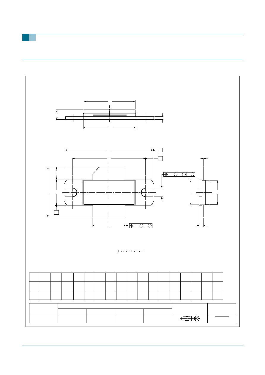
Package outline
Fig 1.
Package outline SOT895-1
REFERENCES
OUTLINE
VERSION
EUROPEAN
PROJECTION
ISSUE DATE
IEC
JEDEC
JEITA
SOT895-1
SOT895-1
05-06-22
05-06-28
DIMENSIONS (mm are the original dimensions)
Plastic flanged cavity package; 2 mounting slots; 2 leads
0
5
10 mm
scale
UNIT
A
mm
D
b
12.83
12.57
0.17
0.14
19.9
19.7
9.78
9.53
19.94
18.92
9.91
9.65
4.1
3.3
c
U
2
0.6
w
2
F
1.14
0.89
U
1
34.16
33.91
L
5.3
4.5
p
3.38
3.12
E
E
1
9.53
9.27
inches
0.505
0.495
0.0065
0.0055
0.785
0.775
D
1
20.42
20.12
0.804
0.792
0.385
0.375
0.785
0.745
0.390
0.380
0.161
0.130
0.023
0.25
w
1
0.01
27.94
1.100
0.045
0.035
1.345
1.335
0.209
0.177
0.133
0.123
Q
1.75
1.50
0.069
0.059
q
0.375
0.365
H
A
D
1
D
F
B
C
A
q
A
B
w1
M
M
M
C
w2
M
M
U
1
L
p
U
2
H
b
1
2
3
E
E
1
Q
c
BLC6G20-140_6G20LS-140_1
© Koninklijke Philips Electronics N.V. 2006. All rights reserved.
Objective data sheet
Rev. 01 -- 30 January 2006
5 of 9
Philips Semiconductors
BLC6G20-140; BLC6G20LS-140
UHF power LDMOS transistor
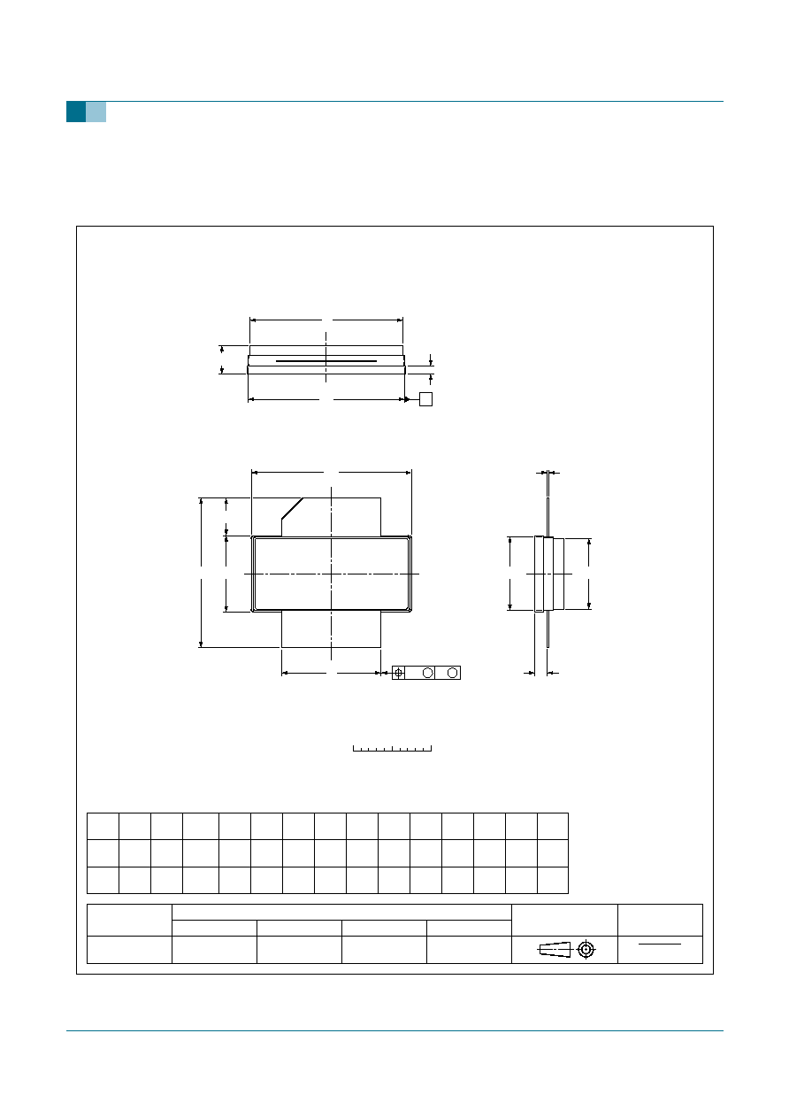
Fig 2.
Package outline SOT896-1
REFERENCES
OUTLINE
VERSION
EUROPEAN
PROJECTION
ISSUE DATE
IEC
JEDEC
JEITA
SOT896-1
SOT896-1
05-06-22
05-06-28
DIMENSIONS (mm are the original dimensions)
Plastic earless flanged cavity package; 2 leads
0
5
10 mm
scale
UNIT
A
mm
D
b
12.83
12.57
0.17
0.14
19.9
19.7
9.78
9.53
19.94
18.92
9.91
9.65
4.1
3.3
c
U
2
0.6
w
2
F
1.14
0.89
U
1
20.70
20.45
L
5.3
4.5
Q
1.75
1.50
E
E
1
9.53
9.27
inches
0.505
0.495
0.0065
0.0055
0.785
0.775
D
1
20.42
20.12
0.804
0.792
0.385
0.375
0.785
0.745
0.390
0.380
0.161
0.130
0.023
0.045
0.035
0.815
0.805
0.209
0.177
0.069
0.059
0.375
0.365
H
A
D
1
D
F
D
3
E
E
1
Q
c
D
w2
M
M
U
1
L
U
2
H
b
1
2
Document Outline