 | ÐлекÑÑоннÑй компоненÑ: BUF04 | СкаÑаÑÑ:  PDF PDF  ZIP ZIP |
Äîêóìåíòàöèÿ è îïèñàíèÿ www.docs.chipfind.ru
FUNCTIONAL BLOCK DIAGRAMS
REV. 0
Information furnished by Analog Devices is believed to be accurate and
reliable. However, no responsibility is assumed by Analog Devices for its
use, nor for any infringements of patents or other rights of third parties
which may result from its use. No license is granted by implication or
otherwise under any patent or patent rights of Analog Devices.
a
Closed-Loop
High Speed Buffer
BUF04*
One Technology Way, P.O. Box 9106, Norwood, MA 02062-9106, U.S.A.
Tel: 617/329-4700
Fax: 617/326-8703
FEATURES
Bandwidth 110 MHz
Slew Rate 3000 V/ s
Low Offset Voltage <1 mV
Very Low Noise < 4 nV/
Hz
Low Supply Current 8.5 mA Mux
Wide Supply Range 5 V to 15 V
Drives Capacitive Loads
Pin Compatible with BUF03
APPLICATIONS
Instrumentation Buffer
RF Buffer
Line Driver
High Speed Current Source
Op Amp Output Current Booster
High Performance Audio
High Speed AD/DA
High slew rate and very low noise and THD, coupled with wide
input and output dynamic range, make the BUF04 an excellent
choice for video and high performance audio circuits.
The BUF04's inherent ability to drive capacitive loads over a
wide voltage and temperature range makes it extremely useful
for a wide variety of applications in military, industrial, and
commercial equipment.
The BUF04 is specified over the extended industrial (40
°
C to
+85
°
C) and military (55
°
C to +125
°
C) temperature range.
BUF04s are available in plastic and ceramic DIP plus SO-8
surface mount packages.
Contact your local sales office for MIL-STD-883 data sheet and
availability.
*Patent pending.
GENERAL DESCRIPTION
The BUF04 is a wideband, closed-loop buffer that combines
state of the art dynamic performance with excellent dc
performance. This combination enables designers to maximize
system performance without any speed versus dc accuracy
compromises.
Built on a high speed Complementary Bipolar (CB) process for
better power performance ratio, the BUF04 consumes less than
8.5 mA operating from
±
5 V or
±
15 V supplies. With a 2000 V/
µ
s
min slew rate, and 100 MHz gain bandwidth product, the
BUF04 is ideally suited for use in high speed applications where
low power dissipation is critical.
Full
±
10 V output swing over the extended temperature range
along with outstanding ac performance and high loop gain
accuracy makes the device useful in high speed data acquisition
systems.
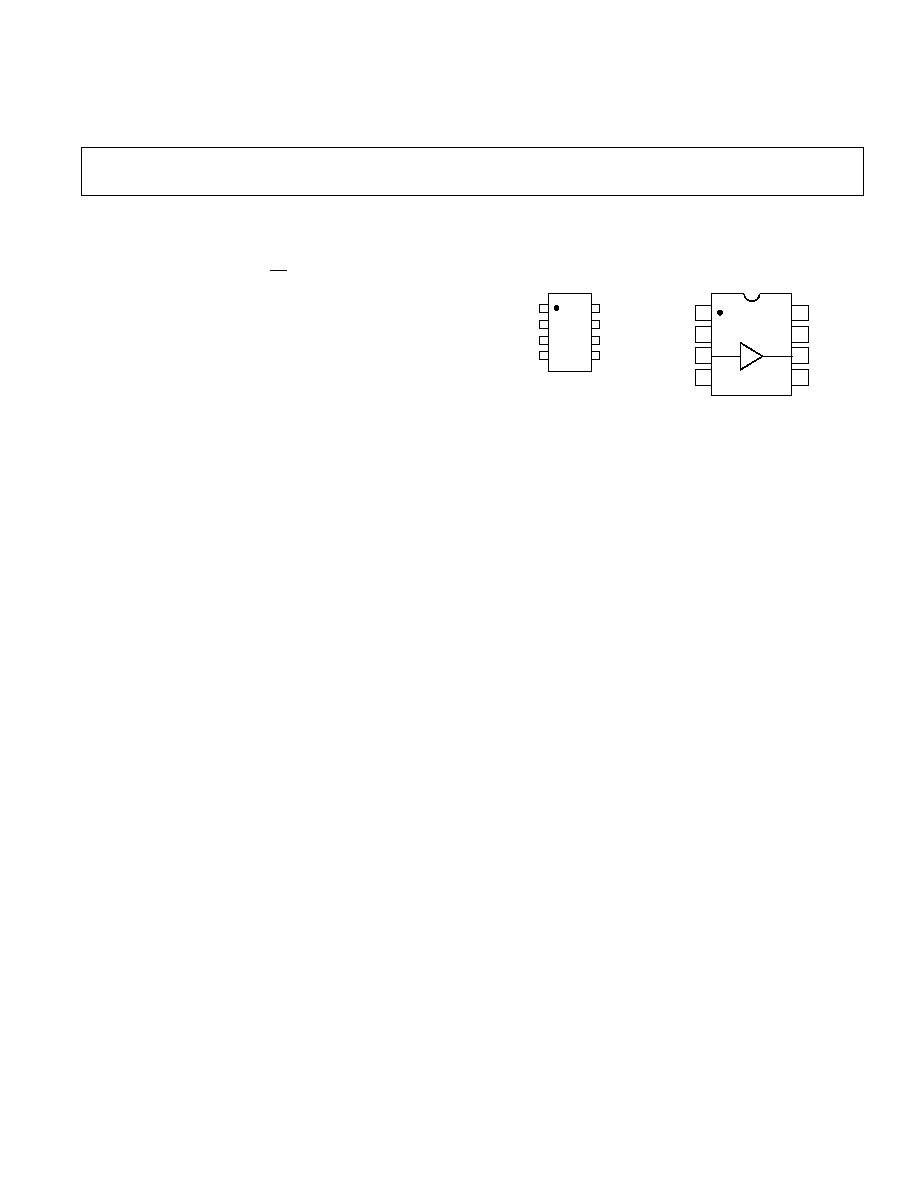
Plastic DIP
8-Lead and Cerdip
(P, Z Suffix)
8-Lead Narrow-Body SO
(S Suffix)
BUF04
1
2
3
4
8
7
6
5
BUF04
NULL
NC
IN
V
NC = NO CONNECT
NULL
OUT
V+
Top View
1
1
NC

BUF04SPECIFICATIONS
ELECTRICAL CHARACTERISTICS
Parameter
Symbol
Conditions
Min
Typ
Max
Units
INPUT CHARACTERISTICS
Offset Voltage
V
OS
0.3
1
mV
40
°
C
T
A
+85
°
C
1.3
4
mV
Input Bias Current
I
B
V
CM
= 0
0.7
5
µ
A
40
°
C
T
A
+85
°
C
2.2
10
µ
A
Input Voltage Range
V
CM
±
13
V
Offset Voltage Drift
V
OS
/
T
30
µ
V/
°
C
Offset Null Range
±
25
mV
OUTPUT CHARACTERISTICS
Output Voltage Swing
V
O
R
L
= 150
,
±
10.5
±
11.1
V
40
°
C
T
A
+85
°
C
±
10
±
11
V
R
L
= 2 k
,
±
13
±
13.5
V
40
°
C
T
A
+85
°
C
±
13
±
13.15
V
Output Current Continuous
I
OUT
±
50
±
65
mA
Peak Output Current
I
OUTP
Note 2
±
80
mA
TRANSFER CHARACTERISTICS
Gain
A
VCL
R
L
= 2 k
0.995
0.9985
1.005
V/V
40
°
C
T
A
+85
°
C
0.995
0.9980
1.005
V/V
Gain Linearity
NL
R
L
= 1 k
, V
O
=
±
10 V
0.005
%
R
L
= 150 k
0.008
%
POWER SUPPLY
Power Supply Rejection Ratio
PSRR
V
S
=
±
4.5 V to
±
18 V
76
93
dB
40
°
C
T
A
+85
°
C
76
93
dB
Supply Current
I
SY
V
O
= 0 V, R
L
=
6.9
8.5
mA
40
°
C
T
A
+85
°
C
6.9
8.5
mA
DYNAMIC PERFORMANCE
Slew Rate
SR
R
L
= 2 k
, C
L
= 70 pF
2000
3000
V/
µ
s
Bandwidth
BW
3 dB, C
L
= 20 pF, R
L
=
110
MHz
Bandwidth
BW
3 dB, C
L
= 20 pF, R
L
= 1 k
110
MHz
Bandwidth
BW
3 dB, C
L
= 20 pF, R
L
= 150
110
MHz
Settling Time
V
IN
=
±
10 V Step to 0.1%
60
ns
Differential Phase
f = 3.58 MHz, R
L
= 150
0.02
Degrees
f = 4.43 MHz, R
L
= 150
0.03
Degrees
Differential Gain
f = 3.58 MHz, R
L
= 150
0.014
%
f = 4.43 MHz, R
L
= 150
0.008
%
Input Capacitance
3
pF
NOISE PERFORMANCE
Voltage Noise Density
e
n
f = 1 kHz
4
nV/
Hz
Current Noise Density
i
n
f = 1 kHz
2
pA/
Hz
NOTE
1
Long term offset voltage is guaranteed by a 1000 hour life test performed on three independent lots at +125
°
C with an LTPD of 1.3.
Specifications subject to change without notice.
REV. 0
2
(@ V
S
= 15.0 V, T
A
= +25 C unless otherwise noted)

ELECTRICAL CHARACTERISTICS
Parameter
Symbol
Conditions
Min
Typ
Max
Units
INPUT CHARACTERISTICS
Offset Voltage
V
OS
0.8
2.0
mV
40
°
C
T
A
+85
°
C
1.0
4
mV
Input Bias Current
I
B
V
CM
= 0 V
0.15
5
µ
A
40
°
C
T
A
+85
°
C
1.6
10
µ
A
Input Voltage Range
V
CM
±
3.0
V
Offset Voltage Drift
V
OS
/
T
30
µ
V/
°
C
Offset Null Range
±
25
mV
OUTPUT CHARACTERISTICS
Output Voltage Swing
V
O
R
L
= 150
,
±
3.0
V
40
°
C
T
A
+85
°
C
±
2.75
±
3.00
V
R
L
= 2 k
,
±
3.0
±
3.6
V
40
°
C
T
A
+85
°
C
±
3.0
±
3.35
V
Output Current - Continuous
I
OUT
±
40
mA
Peak Output Current
I
OUTP
Note 2
±
75
mA
TRANSFER CHARACTERISTICS
Gain
A
VCL
R
L
= 2 k
,
0.995
0.9977
1.005
V/V
40
°
C
T
A
+85
°
C
0.995
1.005
V/V
Gain Linearity
NL
R
L
= 1 k
0.005
%
POWER SUPPLY
Power Supply Rejection Ratio
PSRR
V
S
=
±
4.5 V to
±
18 V
76
93
dB
40
°
C
T
A
+85
°
C
76
93
dB
Supply Current
I
SY
V
O
= 0 V, R
L
=
6.60
8
mA
40
°
C
T
A
+85
°
C
6.70
8
mA
DYNAMIC PERFORMANCE
Slew Rate
SR
R
L
= 2 k
, C
L
= 70 pF
2000
V/
µ
s
Bandwidth
BW
3 dB, C
L
= 20 pF, R
L
=
100
MHz
Bandwidth
BW
3 dB, C
L
= 20 pF, R
L
= 1 k
100
MHz
Bandwidth
BW
3 dB, C
L
= 20 pF, R
L
= 150
100
MHz
Differential Phase
f = 3.58 MHz, R
L
= 150
0.13
Degrees
f = 4.43 MHz, R
L
= 150
0.15
Degrees
Differential Gain
f = 3.58 MHz, R
L
= 150
0.04
%
f = 4.43 MHz, R
L
= 150
0.06
%
NOISE PERFORMANCE
Voltage Noise Density
e
n
f = 1 kHz
4
nV/
Hz
Current Noise Density
i
n
f = 1 kHz
2
pA/
Hz
NOTE
1
Long term offset voltage is guaranteed by a 1000 hour life test performed on three independent lots at +125
°
C, with an LTPD of 1.3.
Specifications subject to change without notice.
(@ V
S
= 5.0 V, T
A
= +25 C unless otherwise noted)
BUF04
REV. 0
3
BUF04
REV. 0
4
WAFER TEST LIMITS
Parameter
Symbol
Conditions
Limit
Units
Offset Voltage
V
OS
V
S
=
±
15 V
1
mV max
V
OS
V
S
=
±
5 V
2
mV max
Input Bias Current
I
B
V
CM
= 0 V
5
µ
A max
Power Supply Rejection Ratio
PSRR
V =
±
4.5 V to
±
18 V
76
dB
Output Voltage Range
V
O
R
L
= 150
±
10.5
V min
Supply Current
I
SY
V
O
= 0 V, R
L
= 2 k
8.5
mA max
Gain
A
VCL
V
O
=
±
10 V, R
L
= 2 k
1
±
0.005
V/V
NOTE
Electrical tests and wafer probe to the limits shown. Due to variations in assembly methods and normal yield loss, yield after packaging is not guaranteed for standard
product dice. Consult factory to negotiate specifications based on dice lot qualifications through sample lot assembly and testing.
ABSOLUTE MAXIMUM RATINGS
1
Supply Voltage . . . . . . . . . . . . . . . . . . . . . . . . . . . . . . . .
±
18 V
Input Voltage . . . . . . . . . . . . . . . . . . . . . . . . . . . . . . . . .
±
18 V
Maximum Power Dissipation . . . . . . . . . . . . . . . See Figure 16
Storage Temperature Range
Z Package . . . . . . . . . . . . . . . . . . . . . . . . . 65
°
C to +175
°
C
P, S Package . . . . . . . . . . . . . . . . . . . . . . . 65
°
C to +150
°
C
Operating Temperature Range
BUF04Z . . . . . . . . . . . . . . . . . . . . . . . . . . 55
°
C to +125
°
C
BUF04S, P . . . . . . . . . . . . . . . . . . . . . . . . . 40
°
C to +85
°
C
Junction Temperature Range
Z Package . . . . . . . . . . . . . . . . . . . . . . . . . 65
°
C to +150
°
C
P, S Package . . . . . . . . . . . . . . . . . . . . . . . 65
°
C to +150
°
C
Lead Temperature Range (Soldering 60 sec) . . . . . . . . +300
°
C
Package Type
JA
2
JC
Units
8-Pin Cerdip (Z)
148
16
°
C/W
8-Pin Plastic DIP (P)
103
43
°
C/W
8-Pin SOIC (S)
158
43
°
C/W
NOTES
1
Absolute maximum ratings apply to both DICE and packaged parts, unless
otherwise noted.
2
JA
is specified for the worst case conditions, i.e.,
JA
is specified for device in socket
for cerdip, P-DIP, and LCC packages;
JA
is specified for device soldered in circuit
board for SOIC package.
ORDERING GUIDE
Temperature
Package
Package
Model
Range
Description
Option
BUF04AZ/883
55
°
C to +125
°
C
Cerdip
Q-8
BUF04GP
40
°
C to +85
°
C
Plastic DIP
N-8
BUF04GS
40
°
C to +85
°
C
SO
SO-8
BUF04GBC
+25
°
C
DICE
DICE
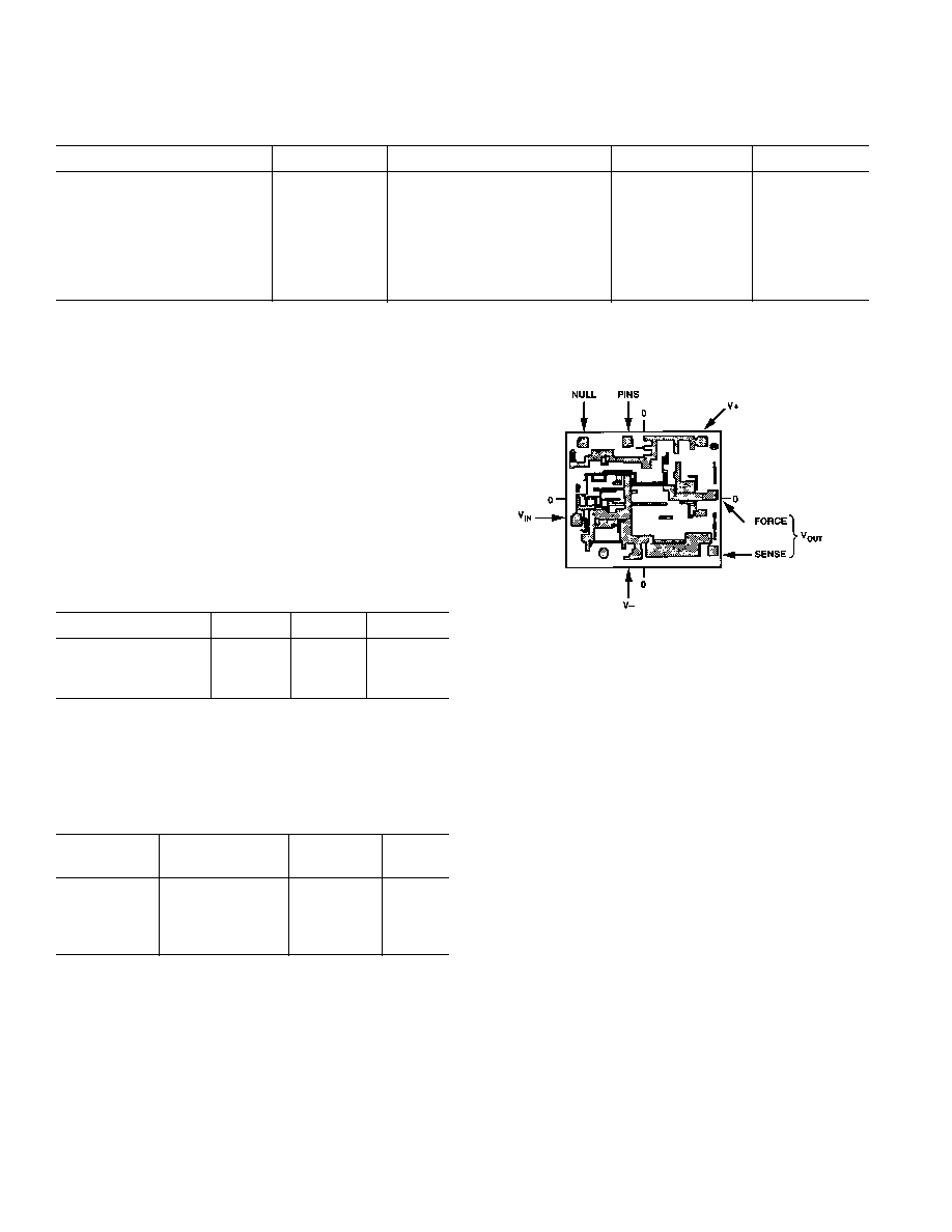
DICE CHARACTERISTICS
BUF04 Die Size 0.075 x 0.064 inch, 5,280 Sq. Mils
Substrate (Die Backside) Is Connected to V+
Transistor Count 45.
(@ V
S
= 15.0 V, T
A
= +25 C unless otherwise noted)
BUF04
REV. 0
5
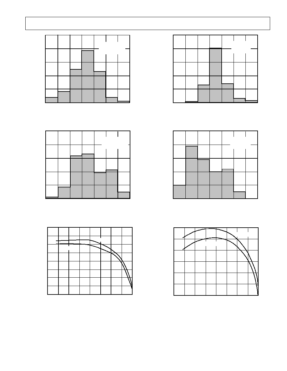
0.6
0.0
0.1
0.5
0.4
0.3
0.2
0.1
OFFSET mV
0
UNITS
150
90
30
60
120
0
30
V
S
= ±15V
315 PLASTIC DIPS
T
A
= +25°C
Figure 1. Input Offset Voltage (V
OS
) Distribution @
±
15 V, P-DIP
1.4
0.2
0
1.2
1.0
0.8
0.6
0.4
OFFSET mV
125
0
75
25
50
100
UNITS
V
S
= ±5V
315 PLASTIC DIPS
T
A
= +25°C
Figure 2. Input Offset Voltage (V
OS
) Distribution @
±
5 V, P-DIP
125
50
75
100
75
50
25
0
25
TEMPERATURE °C
2.0
1.0
5.0
6.0
3.0
4.0
2.0
0
1.0
OFFSET mV
±5V
±15V
Figure 3. Input Offset Voltage (V
OS
) vs. Temperature
Typical Performance Characteristics
200
0
0.2
120
40
0.1
80
0.15
160
0.15
0.1
0.5
0
0.5
OFFSET mV
UNITS
V
S
= ±15V
315 CERDIPS
T
A
= +25°C
Figure 4. Input Offset Voltage (V
OS
) Distribution @
±
15 V, Cerdip
125
0
1.4
75
25
0.2
50
0
100
1.2
1.0
0.8
0.6
0.4
OFFSET mV
UNITS
V
S
= ±5V
315 CERDIPS
T
A
= +25°C
Figure 5. Input Offset Voltage (V
OS
) Distribution @
±
5 V, Cerdip
125
50
75
100
75
50
25
0
25
TEMPERATURE °C
1.0
5.0
6.0
3.0
4.0
2.0
0
INPUT BIAS CURRENT µA
V
S
= ±5V
V
S
= ±15V
Figure 6. Input Bias Current vs. Temperature