BUF04* Closed-Loop High Speed Buffer
FUNCTIONAL BLOCK DIAGRAMS
REV. 0
Information furnished by Analog Devices is believed to be accurate and
reliable. However, no responsibility is assumed by Analog Devices for its
use, nor for any infringements of patents or other rights of third parties
which may result from its use. No license is granted by implication or
otherwise under any patent or patent rights of Analog Devices.
a
Closed-Loop
High Speed Buffer
BUF04*
One Technology Way, P.O. Box 9106, Norwood, MA 02062-9106, U.S.A.
Tel: 617/329-4700
Fax: 617/326-8703
FEATURES
Bandwidth ≠ 110 MHz
Slew Rate ≠ 3000 V/ s
Low Offset Voltage ≠ <1 mV
Very Low Noise ≠ < 4 nV/
Hz
Low Supply Current ≠ 8.5 mA Mux
Wide Supply Range ≠ 5 V to 15 V
Drives Capacitive Loads
Pin Compatible with BUF03
APPLICATIONS
Instrumentation Buffer
RF Buffer
Line Driver
High Speed Current Source
Op Amp Output Current Booster
High Performance Audio
High Speed AD/DA
High slew rate and very low noise and THD, coupled with wide
input and output dynamic range, make the BUF04 an excellent
choice for video and high performance audio circuits.
The BUF04's inherent ability to drive capacitive loads over a
wide voltage and temperature range makes it extremely useful
for a wide variety of applications in military, industrial, and
commercial equipment.
The BUF04 is specified over the extended industrial (≠40
∞
C to
+85
∞
C) and military (≠55
∞
C to +125
∞
C) temperature range.
BUF04s are available in plastic and ceramic DIP plus SO-8
surface mount packages.
Contact your local sales office for MIL-STD-883 data sheet and
availability.
*Patent pending.
GENERAL DESCRIPTION
The BUF04 is a wideband, closed-loop buffer that combines
state of the art dynamic performance with excellent dc
performance. This combination enables designers to maximize
system performance without any speed versus dc accuracy
compromises.
Built on a high speed Complementary Bipolar (CB) process for
better power performance ratio, the BUF04 consumes less than
8.5 mA operating from
±
5 V or
±
15 V supplies. With a 2000 V/
µ
s
min slew rate, and 100 MHz gain bandwidth product, the
BUF04 is ideally suited for use in high speed applications where
low power dissipation is critical.
Full
±
10 V output swing over the extended temperature range
along with outstanding ac performance and high loop gain
accuracy makes the device useful in high speed data acquisition
systems.
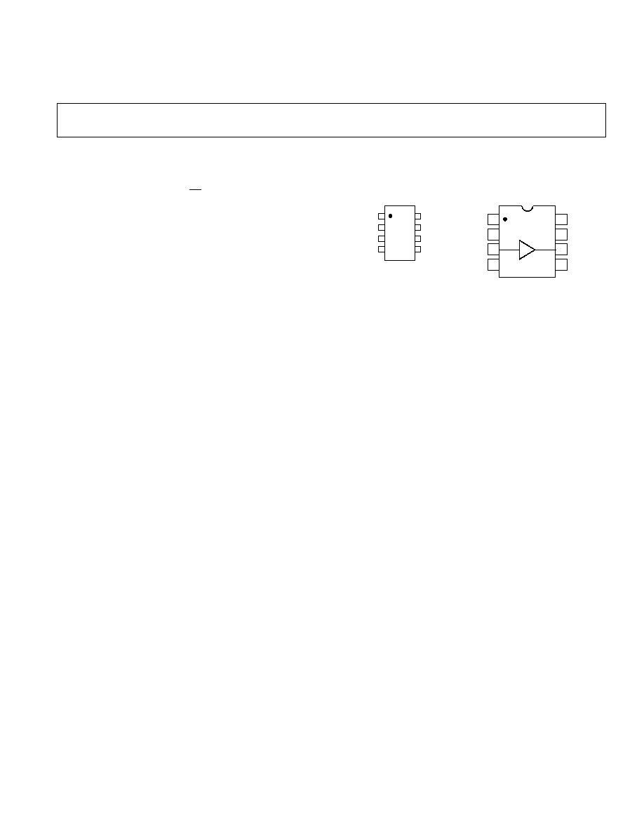
Plastic DIP
8-Lead and Cerdip
(P, Z Suffix)
8-Lead Narrow-Body SO
(S Suffix)
BUF04
1
2
3
4
8
7
6
5
BUF04
NULL
NC
IN
V≠
NC = NO CONNECT
NULL
OUT
V+
Top View
1
1
NC

BUF04≠SPECIFICATIONS
ELECTRICAL CHARACTERISTICS
Parameter
Symbol
Conditions
Min
Typ
Max
Units
INPUT CHARACTERISTICS
Offset Voltage
V
OS
0.3
1
mV
≠40
∞
C
T
A
+85
∞
C
1.3
4
mV
Input Bias Current
I
B
V
CM
= 0
0.7
5
µ
A
≠40
∞
C
T
A
+85
∞
C
2.2
10
µ
A
Input Voltage Range
V
CM
±
13
V
Offset Voltage Drift
V
OS
/
T
30
µ
V/
∞
C
Offset Null Range
±
25
mV
OUTPUT CHARACTERISTICS
Output Voltage Swing
V
O
R
L
= 150
,
±
10.5
±
11.1
V
≠40
∞
C
T
A
+85
∞
C
±
10
±
11
V
R
L
= 2 k
,
±
13
±
13.5
V
≠40
∞
C
T
A
+85
∞
C
±
13
±
13.15
V
Output Current ≠ Continuous
I
OUT
±
50
±
65
mA
Peak Output Current
I
OUTP
Note 2
±
80
mA
TRANSFER CHARACTERISTICS
Gain
A
VCL
R
L
= 2 k
0.995
0.9985
1.005
V/V
≠40
∞
C
T
A
+85
∞
C
0.995
0.9980
1.005
V/V
Gain Linearity
NL
R
L
= 1 k
, V
O
=
±
10 V
0.005
%
R
L
= 150 k
0.008
%
POWER SUPPLY
Power Supply Rejection Ratio
PSRR
V
S
=
±
4.5 V to
±
18 V
76
93
dB
≠40
∞
C
T
A
+85
∞
C
76
93
dB
Supply Current
I
SY
V
O
= 0 V, R
L
=
6.9
8.5
mA
≠40
∞
C
T
A
+85
∞
C
6.9
8.5
mA
DYNAMIC PERFORMANCE
Slew Rate
SR
R
L
= 2 k
, C
L
= 70 pF
2000
3000
V/
µ
s
Bandwidth
BW
≠3 dB, C
L
= 20 pF, R
L
=
110
MHz
Bandwidth
BW
≠3 dB, C
L
= 20 pF, R
L
= 1 k
110
MHz
Bandwidth
BW
≠3 dB, C
L
= 20 pF, R
L
= 150
110
MHz
Settling Time
V
IN
=
±
10 V Step to 0.1%
60
ns
Differential Phase
f = 3.58 MHz, R
L
= 150
0.02
Degrees
f = 4.43 MHz, R
L
= 150
0.03
Degrees
Differential Gain
f = 3.58 MHz, R
L
= 150
0.014
%
f = 4.43 MHz, R
L
= 150
0.008
%
Input Capacitance
3
pF
NOISE PERFORMANCE
Voltage Noise Density
e
n
f = 1 kHz
4
nV/
Hz
Current Noise Density
i
n
f = 1 kHz
2
pA/
Hz
NOTE
1
Long term offset voltage is guaranteed by a 1000 hour life test performed on three independent lots at +125
∞
C with an LTPD of 1.3.
Specifications subject to change without notice.
REV. 0
≠2≠
(@ V
S
= 15.0 V, T
A
= +25 C unless otherwise noted)

ELECTRICAL CHARACTERISTICS
Parameter
Symbol
Conditions
Min
Typ
Max
Units
INPUT CHARACTERISTICS
Offset Voltage
V
OS
0.8
2.0
mV
≠40
∞
C
T
A
+85
∞
C
1.0
4
mV
Input Bias Current
I
B
V
CM
= 0 V
0.15
5
µ
A
≠40
∞
C
T
A
+85
∞
C
1.6
10
µ
A
Input Voltage Range
V
CM
±
3.0
V
Offset Voltage Drift
V
OS
/
T
30
µ
V/
∞
C
Offset Null Range
±
25
mV
OUTPUT CHARACTERISTICS
Output Voltage Swing
V
O
R
L
= 150
,
±
3.0
V
≠40
∞
C
T
A
+85
∞
C
±
2.75
±
3.00
V
R
L
= 2 k
,
±
3.0
±
3.6
V
≠40
∞
C
T
A
+85
∞
C
±
3.0
±
3.35
V
Output Current - Continuous
I
OUT
±
40
mA
Peak Output Current
I
OUTP
Note 2
±
75
mA
TRANSFER CHARACTERISTICS
Gain
A
VCL
R
L
= 2 k
,
0.995
0.9977
1.005
V/V
≠40
∞
C
T
A
+85
∞
C
0.995
1.005
V/V
Gain Linearity
NL
R
L
= 1 k
0.005
%
POWER SUPPLY
Power Supply Rejection Ratio
PSRR
V
S
=
±
4.5 V to
±
18 V
76
93
dB
≠40
∞
C
T
A
+85
∞
C
76
93
dB
Supply Current
I
SY
V
O
= 0 V, R
L
=
6.60
8
mA
≠40
∞
C
T
A
+85
∞
C
6.70
8
mA
DYNAMIC PERFORMANCE
Slew Rate
SR
R
L
= 2 k
, C
L
= 70 pF
2000
V/
µ
s
Bandwidth
BW
≠3 dB, C
L
= 20 pF, R
L
=
100
MHz
Bandwidth
BW
≠3 dB, C
L
= 20 pF, R
L
= 1 k
100
MHz
Bandwidth
BW
≠3 dB, C
L
= 20 pF, R
L
= 150
100
MHz
Differential Phase
f = 3.58 MHz, R
L
= 150
0.13
Degrees
f = 4.43 MHz, R
L
= 150
0.15
Degrees
Differential Gain
f = 3.58 MHz, R
L
= 150
0.04
%
f = 4.43 MHz, R
L
= 150
0.06
%
NOISE PERFORMANCE
Voltage Noise Density
e
n
f = 1 kHz
4
nV/
Hz
Current Noise Density
i
n
f = 1 kHz
2
pA/
Hz
NOTE
1
Long term offset voltage is guaranteed by a 1000 hour life test performed on three independent lots at +125
∞
C, with an LTPD of 1.3.
Specifications subject to change without notice.
(@ V
S
= 5.0 V, T
A
= +25 C unless otherwise noted)
BUF04
REV. 0
≠3≠
BUF04
REV. 0
≠4≠
WAFER TEST LIMITS
Parameter
Symbol
Conditions
Limit
Units
Offset Voltage
V
OS
V
S
=
±
15 V
1
mV max
V
OS
V
S
=
±
5 V
2
mV max
Input Bias Current
I
B
V
CM
= 0 V
5
µ
A max
Power Supply Rejection Ratio
PSRR
V =
±
4.5 V to
±
18 V
76
dB
Output Voltage Range
V
O
R
L
= 150
±
10.5
V min
Supply Current
I
SY
V
O
= 0 V, R
L
= 2 k
8.5
mA max
Gain
A
VCL
V
O
=
±
10 V, R
L
= 2 k
1
±
0.005
V/V
NOTE
Electrical tests and wafer probe to the limits shown. Due to variations in assembly methods and normal yield loss, yield after packaging is not guaranteed for standard
product dice. Consult factory to negotiate specifications based on dice lot qualifications through sample lot assembly and testing.
ABSOLUTE MAXIMUM RATINGS
1
Supply Voltage . . . . . . . . . . . . . . . . . . . . . . . . . . . . . . . .
±
18 V
Input Voltage . . . . . . . . . . . . . . . . . . . . . . . . . . . . . . . . .
±
18 V
Maximum Power Dissipation . . . . . . . . . . . . . . . See Figure 16
Storage Temperature Range
Z Package . . . . . . . . . . . . . . . . . . . . . . . . . ≠65
∞
C to +175
∞
C
P, S Package . . . . . . . . . . . . . . . . . . . . . . . ≠65
∞
C to +150
∞
C
Operating Temperature Range
BUF04Z . . . . . . . . . . . . . . . . . . . . . . . . . . ≠55
∞
C to +125
∞
C
BUF04S, P . . . . . . . . . . . . . . . . . . . . . . . . . ≠40
∞
C to +85
∞
C
Junction Temperature Range
Z Package . . . . . . . . . . . . . . . . . . . . . . . . . ≠65
∞
C to +150
∞
C
P, S Package . . . . . . . . . . . . . . . . . . . . . . . ≠65
∞
C to +150
∞
C
Lead Temperature Range (Soldering 60 sec) . . . . . . . . +300
∞
C
Package Type
JA
2
JC
Units
8-Pin Cerdip (Z)
148
16
∞
C/W
8-Pin Plastic DIP (P)
103
43
∞
C/W
8-Pin SOIC (S)
158
43
∞
C/W
NOTES
1
Absolute maximum ratings apply to both DICE and packaged parts, unless
otherwise noted.
2
JA
is specified for the worst case conditions, i.e.,
JA
is specified for device in socket
for cerdip, P-DIP, and LCC packages;
JA
is specified for device soldered in circuit
board for SOIC package.
ORDERING GUIDE
Temperature
Package
Package
Model
Range
Description
Option
BUF04AZ/883
≠55
∞
C to +125
∞
C
Cerdip
Q-8
BUF04GP
≠40
∞
C to +85
∞
C
Plastic DIP
N-8
BUF04GS
≠40
∞
C to +85
∞
C
SO
SO-8
BUF04GBC
+25
∞
C
DICE
DICE
DICE CHARACTERISTICS
BUF04 Die Size 0.075 x 0.064 inch, 5,280 Sq. Mils
Substrate (Die Backside) Is Connected to V+
Transistor Count 45.
(@ V
S
= 15.0 V, T
A
= +25 C unless otherwise noted)
BUF04
REV. 0
≠5≠
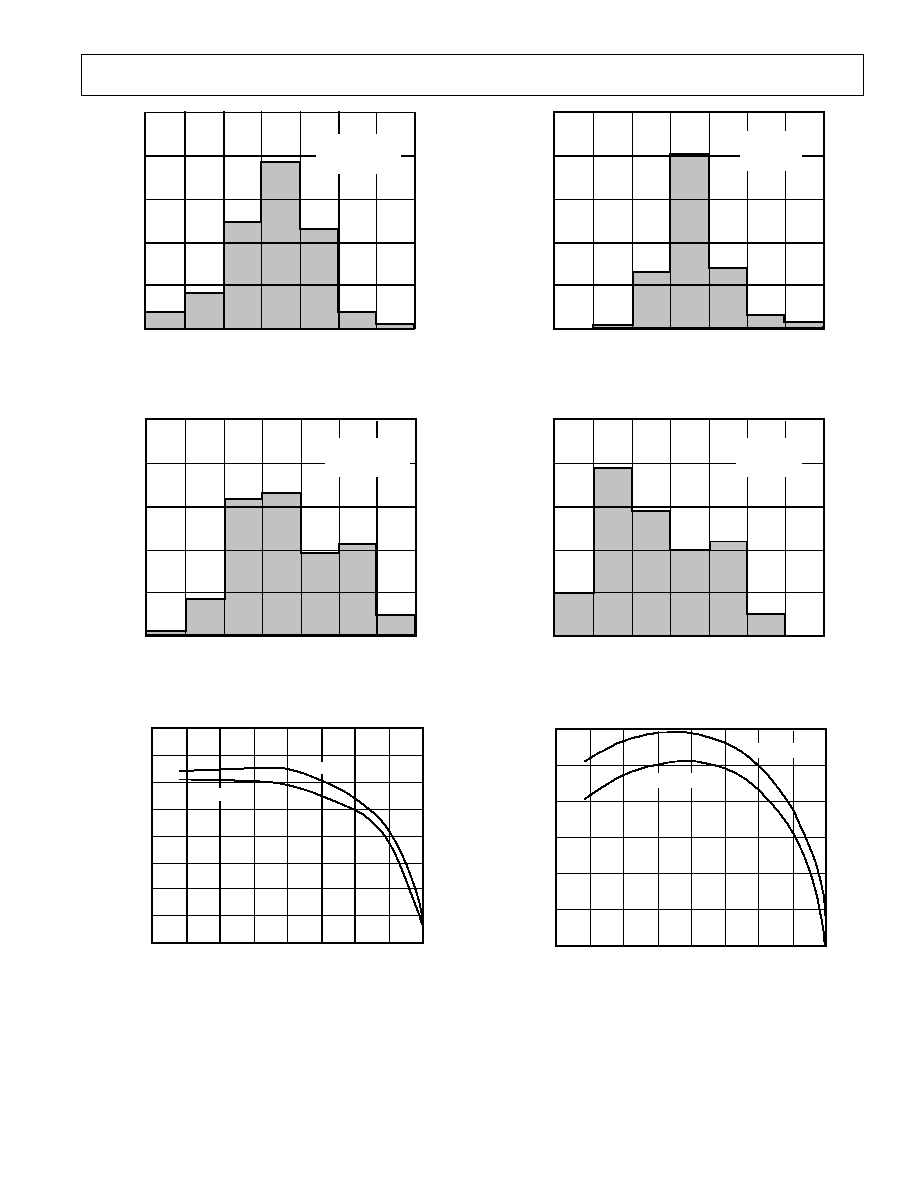
0.6
0.0
≠0.1
0.5
0.4
0.3
0.2
0.1
OFFSET ≠ mV
0
UNITS
150
90
30
60
120
0
30
V
S
= ±15V
315 PLASTIC DIPS
T
A
= +25∞C
Figure 1. Input Offset Voltage (V
OS
) Distribution @
±
15 V, P-DIP
1.4
0.2
0
1.2
1.0
0.8
0.6
0.4
OFFSET ≠ mV
125
0
75
25
50
100
UNITS
V
S
= ±5V
315 PLASTIC DIPS
T
A
= +25∞C
Figure 2. Input Offset Voltage (V
OS
) Distribution @
±
5 V, P-DIP
125
≠50
≠75
100
75
50
25
0
≠25
TEMPERATURE ≠ ∞C
2.0
≠1.0
≠5.0
≠6.0
≠3.0
≠4.0
≠2.0
0
1.0
OFFSET ≠ mV
±5V
±15V
Figure 3. Input Offset Voltage (V
OS
) vs. Temperature
Typical Performance Characteristics≠
200
0
0.2
120
40
≠0.1
80
≠0.15
160
0.15
0.1
0.5
0
≠0.5
OFFSET ≠ mV
UNITS
V
S
= ±15V
315 CERDIPS
T
A
= +25∞C
Figure 4. Input Offset Voltage (V
OS
) Distribution @
±
15 V, Cerdip
125
0
1.4
75
25
0.2
50
0
100
1.2
1.0
0.8
0.6
0.4
OFFSET ≠ mV
UNITS
V
S
= ±5V
315 CERDIPS
T
A
= +25∞C
Figure 5. Input Offset Voltage (V
OS
) Distribution @
±
5 V, Cerdip
125
≠50
≠75
100
75
50
25
0
≠25
TEMPERATURE ≠ ∞C
≠1.0
≠5.0
≠6.0
≠3.0
≠4.0
≠2.0
0
INPUT BIAS CURRENT ≠ µA
V
S
= ±5V
V
S
= ±15V
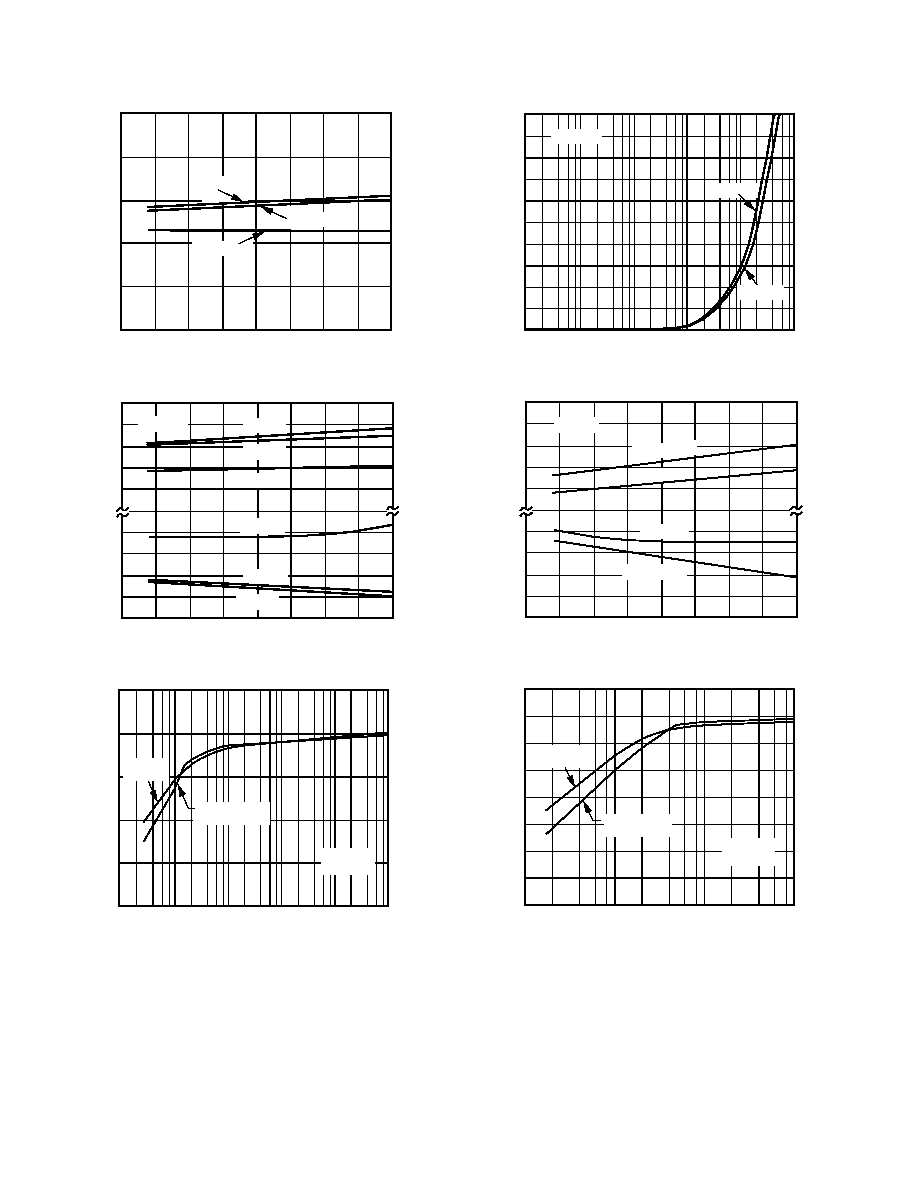
Figure 6. Input Bias Current vs. Temperature
BUF04
REV. 0
≠6≠
125
≠50
≠75
100
75
50
25
0
≠25
TEMPERATURE ≠ ∞C
8.0
5.5
7.0
6.0
6.5
7.5
SUPPLY CURRENT ≠ mA
V
S
= ±18V
V
S
= ±5V
V
S
= ±15V
Figure 7. Supply Current vs. Temperature
15
≠15
≠12
≠14
≠13
11
≠11
12
13
14
OUTPUT SWING ≠ Volts
V
S
= ±15V
R
L
= 1k
R
L
= 1k
R
L
= 150
125
≠50
≠75
100
75
50
25
0
≠25
TEMPERATURE ≠ ∞C
R
L
= 150
R
L
= 2k
R
L
= 2k
Figure 8. Output Voltage Swing vs. Temperature @
±
15 V
ABS NEGATIVE
SWING
V
S
= ±5V
T
A
= +25∞C
10
100
1M
100k
10k
1k
LOAD RESISTANCE ≠
5
4
0
3
2
1
OUTPUT SWING ≠ Volts
POSITIVE
SWING
Figure 9. Maximum V
OUT
Swing vs. Load @
±
5 V
T
A
= +25∞C
V
S
= ±5V
1k
10k
100M
10M
1M
100k
FREQUENCY ≠ Hz
50
25
0
30
35
40
45
5
10
15
20
OUTPUT IMPEDANCE ≠
V
S
= ±15V
Figure 10. Output Impedance vs. Frequency
5.0
≠5.0
≠3.5
≠4.5
≠4.0
3.0
≠3.0
3.5
4.0
4.5
OUTPUT SWING ≠ Volts
V
S
= ±5V
R
L
= 2k , 1k
R
L
= 150
125
≠50
≠75
100
75
50
25
0
≠25
TEMPERATURE ≠ ∞C
R
L
= 150
R
L
= 2k , 1k
Figure 11. Output Voltage Swing vs. Temperature @
±
5 V
V
S
= ±15V
T
A
= +25∞C
10
100
10k
1k
LOAD RESISTANCE ≠
16
8
0
4
12
14
10
6
2
OUTPUT SWING ≠ Volts
POSITIVE
SWING
ABS NEGATIVE
SWING
Figure 12. Maximum V
OUT
Swing vs. Load @
±
15 V
BUF04
REV. 0
≠7≠
10
≠8
≠10
8
6
4
2
0
≠2
≠4
≠6
COMMON MODE VOLTAGE ≠ Volts
0.5
≠2.0
≠0.5
≠1.5
≠1.0
0
INPUT BIAS CURRENT ≠ µA
T
A
= +25∞C
Figure 13. Bias Current vs. Input Voltage
1k
10k
100M
10M
1M
100k
FREQUENCY ≠ Hz
100
50
0
60
70
80
90
10
20
30
40
POWER SUPPLY REJECTION ≠ dB
T
A
= +25∞C
V
S
= ±5, ±15V
+PSRR
≠ PSRR
Figure 14. Power Supply Rejection vs. Frequency
6000
0
3000
1000
2000
5000
4000
SLEW RATE ≠ V/µs
125
≠50
≠75
100
50
25
0
75
≠25
TEMPERATURE ≠ ∞C
V
S
= ±15V
+EDGE
≠EDGE
Figure 15. Slew Rate vs. Temperature
0
125
25
100
75
50
85
TEMPERATURE ≠
∞
C
0
1.5
1.0
0.5
POWER DISSIPATION ≠ W
T
J
MAX = 150∞C
FREE AIR
NO HEAT SINK
JA
= 148∞C/W
JA
= 158∞C/W
JA
= 103∞C/W
P DIP
CERDIP
SOIC
Figure 16. Maximum Power Dissipation vs.
Ambient Temperature
10
0
100
1
10
1M
100k
10k
1k
100
FREQUENCY ≠ Hz
INPUT NOISE VOLTAGE
SPECTRAL DENSITY ≠ nV/ Hz
Figure 17. Input Noise Voltage vs. Frequency
250
50
0
200
150
100
CAPACITIVE LOAD ≠ pF
6000
0
3000
1000
2000
5000
4000
SLEW RATE ≠ V/µs
POSITIVE
SLEW RATE
NEGATIVE
SLEW RATE
V
S
= ±15V
SWING = ±10V
T
A
= +25∞C
Figure 18. Slew Rate vs. Capacitive Loads
BUF04
REV. 0
≠8≠
250
50
0
200
150
100
CAPACITANCE ≠ pF
150
0
75
25
50
125
100
BANDWIDTH ≠ MHz
PHASE ≠ Deg
≠45
≠180
≠112.5
≠157.5
≠135
≠67.5
≠90
T
A
= +25∞C
V
S
= ±5V
PHASE @
R
L
= 150
PHASE @
R
L
= 2k
BANDWIDTH
Figure 19. Bandwidth and Phase vs.
Capacitive Loads @
±
5 V
±15
±10
±5
SUPPLY VOLTAGE ≠Volts
140
80
110
90
100
130
120
BANDWIDTH ≠ MHz
R
L
= 2k
≠55∞C
+25∞C
+125∞C
Figure 20. Bandwidth vs. Supply Voltage and
Temperature
10
≠8
≠10
8
4
2
0
6
≠2
≠4
≠6
OUTPUT VOLTAGE ≠ Volts
1.5
≠1.5
0
≠1.0
≠0.5
1.0
0.5
GAIN DEVIATION ≠ dB
6
≠6
0
≠4
≠2
4
2
PHASE DEVIATION ≠ Degrees
PHASE
GAIN
V
S
= ±15V
V
IN
= 0.1V
RMS
FREQUENCY = 10MHz
R
L
= 150
Figure 21. Gain and Phase Deviation, R
L
= 150
250
50
0
200
150
100
CAPACITANCE ≠ pF
150
0
75
25
50
125
100
BANDWIDTH ≠ MHz
PHASE ≠ Deg
≠45
≠180
≠112.5
≠157.5
≠135
≠67.5
≠90
T
A
= +25∞C
V
S
= ±15V
R
L
= 150
R
L
= 2k
BANDWIDTH
PHASE
Figure 22. Bandwidth & Phase vs.
Capacitive Loads @
±
15 V
100
1k
10k
RESISTIVE LOAD ≠
200
100
0
50
150
BANDWIDTH ≠ MHz
T
A
= +25∞C
V
S
= ±15V
Figure 23. Bandwidth vs. Loads
10
≠8
≠10
8
4
2
0
6
≠2
≠4
≠6
OUTPUT VOLTAGE ≠ Volts
0.075
≠0.075
0
≠0.050
≠0.025
0.050
0.025
GAIN DEVIATION ≠ dB
PHASE
GAIN
V
S
= ±15V
V
IN
= 0.1V
RMS
FREQUENCY = 10MHz
R
L
= 2k
PHASE DEVIATION ≠ Degrees
≠1.5
0
≠1.0
≠0.5
1.0
0.5
1.5
Figure 24. Gain and Phase Deviation, R
L
= 2 k
BUF04
REV. 0
≠9≠
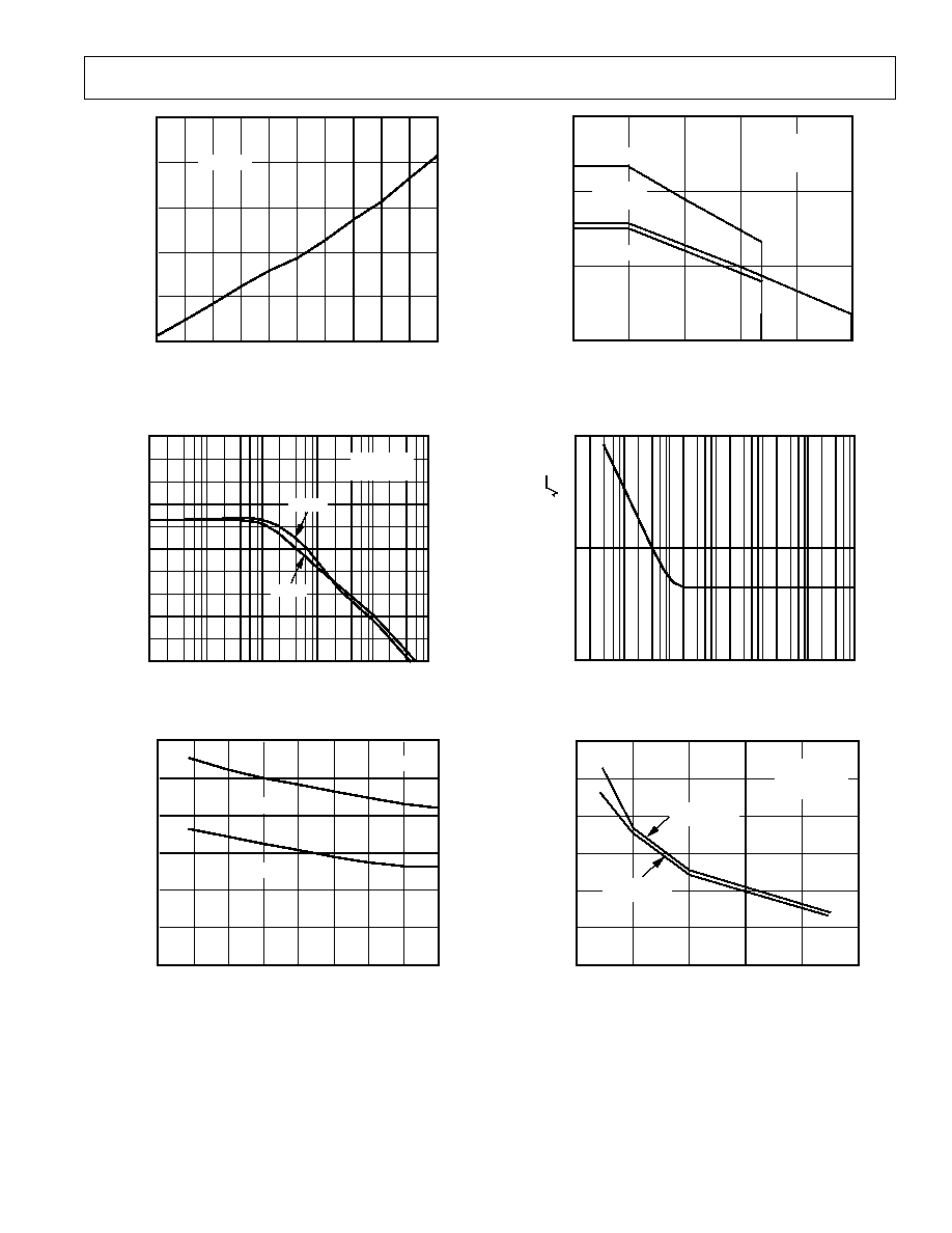
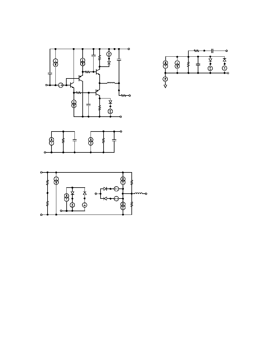
FUNCTIONAL DESCRIPTION
The BUF04 is a closed-loop voltage buffer based on a current
feedback architecture. Its high open-loop transimpedance, high
output current drive capability, and its low input offset voltage
makes it useful in a variety of applications, such as buffering the
inputs of sampling and flash A/D converters, audio and video
line drivers, active filters, and precision op amp hoosters.
A transistor-level equivalent circuit for the BUF04 is illustrated
in Figure 29. The input stage consists of a pair of emitter
follower transistors, Q1 and Q2, whose outputs drive a second
set of transistors, Q3 and Q4. The emitters of Q3 and Q4 are
connected together through diodes, D1 and D2, to form a low
impedance input for the feedback signal (in current mode) from
the output stage. The outputs of Q3 and Q4 are then
"mirrored" to Q5 and Q6 which form the gain stage of the
BUF04. The signal is taken from the collectors of Q5 and Q6
which drive a "Darlington-connected" output stage made up of
transistors Q7-Q10. Three R-C networks (R1≠C1, R2≠C2, and
R3≠C3) form feed-forward paths which bypass certain sections
of the BUF04 for improved high frequency performance and
capacitive load drive capability. Since the signal conveyed
internally in the BUF04 is a current, the frequency response
and slew rate of the BUF04 are insensitive to supply voltage
variations.
12
0
≠12
10k
100k
1000M
100M
10M
1M
3
6
9
≠9
≠6
≠3
GAIN ≠ dB
FREQUENCY ≠ Hz
V
S
= ±15V
T
A
= +25
∞
C
R
L
= 150
C
L
= 100pF
C
L
= 50pF
C
L
= 0pF
150
CL
10
BUF04
Figure 28. Bandwidth vs. Frequency
Q11
Q13
Q5
Q3
Q7
Q9
Q2
Q1
C1
C3
R3
D2
D1
Q4
R2
Q10
Q8
Q6
Q14
Q12
V
IN
V
OUT
C2
R
FB
100
20
20
Figure 29. Transistor-Level Equivalent Circuit
An interesting feature of the BUF04 architecture is the use of
"slew-enhancement" transistors, Q11≠Q14. Under normal small
signal (V
IN
< 2 V
be
s) conditions, these transistors are normally
"OFF." In large signals, high speed transient applications where
the input signal is > 2 V
be
s, these transistors turn on and literally
"brute-force" the output to follow the input. When the input
signal drops below 2 V
be
s, the transistors return to their
normally "OFF" state.
10
100
0%
90
50mV
10ns
50mV
INPUT
(50mV/DIV)
OUTPUT
(50mV/DIV)
V
S
= ±15V, R
L
= 2k
, C
L
= 15pF
Figure 25. Small-Signal Transient Response
10
100
0%
90
2V
50ns
2V
INPUT
(2V/DIV)
OUTPUT
(2V/DIV)
V
S
= ±15V, R
L
= 2k
, C
L
= 15pF
DLY 375.0ns
Figure 26. Large-Signal Transient Response
0.1
0.010
0.001
0.0001
20
100
1k
10k
20k
07 MAR 93 21:31:53
AUDIO PRECISION BUF04 THD+N (%) vs FREQ (Hz)
T
A
D
B
C
VS= ±15V
LPF=80kHz
: VIN = 0.775Vrms, RL= 150W
: VIN = 0.775Vrms, RL= 600W
A : VIN = 7.75Vrms, RL= 150W
B : VIN = 7.75Vrms, RL= 600W
A
B
C
D
C
C
D
Figure 27. THD + Noise vs. Amplitude
BUF04
REV. 0
≠10≠
A two-terminal equivalent circuit of the BUF04 is shown in
Figure 30 where the transistor-level equivalent circuit is reduced
to its essential elements. The input stage develops a signal
current, I
IN
, that is replicated by an internal current conveyor so
as to flow through R
t
, the transimpedance of the BUF04. The
voltage developed across R
t
is buffered by a unity-gain output
voltage follower. With an open-loop R
t
of 400 k
and an R
IN
of
30
, the voltage gain of the BUF04, given by the ratio R
t
/R
IN
is
approximately 13,000--accurate to approximately 13.5 bits.
The BUF04's open-loop ac transimpedance response is
determined by the open-loop pole formed by R
t
and C
t
. Since
C
t
is typically 8 pF, the open-loop pole occurs at approximately
50 kHz.
X1
I
IN
R
t
R
IN
I
IN
V
OUT
C
t
V
IN
XI
R
FB
R
IN
= 30
R
t
= 400 k
C
t
= 8pF
RFB = 100
Figure 30. Current-Feedback Functional Equivalent
Circuit of the BUF04
Grounding and Bypassing Considerations
To take full advantage of the BUF04's very wide bandwidth,
high slew rates, and dynamic range capabilities requires due
diligence with regard to supply bypassing. In high speed circuits,
the supply bypassing network must provide a very low impedance
return path for currents flowing to and from the load network.
As with any high speed application, multiple bypassing is always
recommended. A 10
µ
F tantalum electrolytic in parallel with a
0.1
µ
F ceramic capacitor is sufficient for most applications. For
those high speed applications where output load currents
approach 50 mA, small valued resistors (1.1
to 4.7
) in
series with the tantalum capacitors may improve circuit
transient response by damping out the capacitor's self-
inductance. Figure 31 illustrates bypassing recommendations.
BUF04
7
6
10µF R1
0.1µF
V+
0.1µF
V≠
10µF
R2
4
3
R
S
R
L
KELVIN RETURN
FOR LOAD CURRENT
KELVIN RETURN
FOR LOAD CURRENT
V
IN
V
OUT
NOTE
USE SHORT LEAD LENGTHS (<5mm)
Figure 31. Recommended Power-Supply Bypassing
To minimize the effects of high-frequency coupling, circuits
must be built with short interconnect leads, and large ground
planes should he used whenever possible to provide a low
resistance, low-inductance circuit path. Sockets should be
avoided because the increased interlead capacitance can degrade
bandwidth and stability. If sockets are necessary, individual pin
sockets (oftentimes called "cage jacks," AMP Part No.
5-330808-3 or 5-330808-6) should be used. They contribute far
less stray reactance than molded socket assemblies.
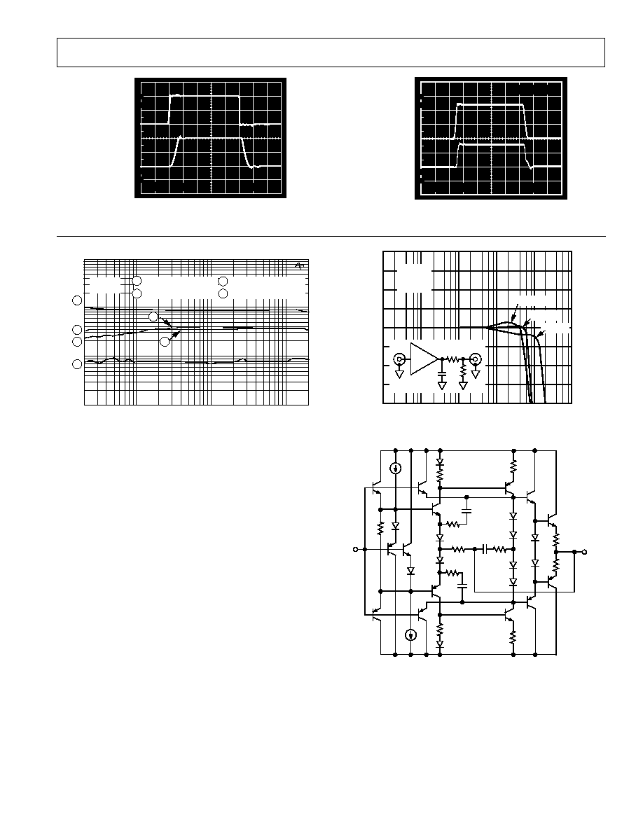
Offset Voltage Nulling
Although the offset voltage of the BUF04 is very low (1 mV,
maximum) for such a high speed buffer, the circuit shown in
Figure 32 can be used if additional offset voltage nulling is
required. A potentiometer ranging from 1 k to 10 k can be used
for V
OS
nulling; with a 10 k
potentiometer, the trim range is
±
30 mV.
V+
BUF04
7
6
10µF
0.1µF
0.1µF
V≠
10µF
4
3
V
IN
10k
1
V
OUT
TRIM RANGE
±30mV
8
Figure 32. Optional Offset Voltage Nulling Scheme
APPLICATIONS
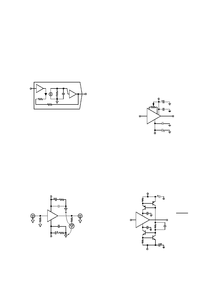
Output Short-Circuit Protection
To optimize the transient response and output voltage swing of
the BUF04, internal output short-circuit current limiting was
omitted. Although the BUF04 can provide continuous output
currents of 50 mA without protection, direct connection of the
BUF04's output to ground or to the supplies will destroy the
device. An active current limit technique, illustrated in Figure
33, provides the necessary short-circuit protection while
retaining full dc output voltage swing to the load.
BUF04
7
6
10µF
0.1µF
0.1µF
≠15V
10µF
4
3
V
IN
V
OUT
+15V
RSC2
10
2N2219
2N2219
2N2905
2N2905
RSC1
10
0.01µF
SET ISC +(ISC≠) <60mA,
CONTINUOUS
RSC1 (RSC2) =
0.6V
ISC + (ISC≠)
6.2k
Figure 33. Short-Circuit Current Limiting Using
Current Sources
BUF04
REV. 0
≠11≠
Output Current Transient Recovery
Settling characteristics of high speed buffers also include the
buffer's ability to recover, i.e., settle, from a transient output
current load condition. When driving the input of an A/D
converter, especially the successive-approximation converter
types, the buffer must maintain a constant output voltage under
dynamically changing load current conditions. In these types of
converters, the comparison point is usually diode-clamped, but
it may deviate several hundred millivolts resulting in high
frequency modulation of the A/D input current. Open-loop and
closed-loop buffers (also, op amps configured as followers) that
exhibit high closed-loop output impedances and/or low unity
gain crossover frequencies recover very slowly from output load
current transients. This slow recovery leads to linearity errors or
missing codes because of errors in the instantaneous input volt-
age. Therefore, the buffer (or op amp) chosen for this type of
application should exhibit low output impedance and high unity
gain bandwidth so that its output has had a chance to settle to
its nominal value before the converter makes its comparison.
The circuit in Figure 34 illustrates a settling measurement
circuit for evaluating the recovery time of high speed buffers
from an output load current transient. The input to the buffer is
grounded for ease of measuring the recovery time, and two
resistors are used to sum steady-state and transient load currents
at the output. As a worst-case condition, R1, was chosen such
that the BUF04 would source (or sink) a steady-state current of
25 mA. R2 was then chosen to add a 10 mA transient current
upon the steady-state value. To set accurately the nodal voltages
internal to the BUF04, the supply voltages were offset by the
voltage applied to R1. Because of its high transimpedance, wide
bandwidth, and low output impedance, the BUF04 exhibits an
extremely fast recovery time of 60 ns to 0.01%, as shown in
Figure 34. Results were identical regardless whether the BUF04
was sourcing or sinking current.
BUF04
7
6
0.1µF
0.1µF
10µF
4
3
TP2
TP1
R2
250
10µF
R1
200
V
LOAD
V+
SOURCE: ≠5V
SINK: +5V
V
IN
SOURCE: 0
≠2.5 V
SINK: 0
+2.5V
V≠
Figure 34. Transient Output Load Current Test Circuit
10
90
100
0%
5mV
59.00ns
20ns
100mV
t
I
SOURCE
(4mA/DIV)
V
OUT
(5mV/DIV)
35mA
25mA
Figure 35. BUF04's Output Load Current Recovery Time
Terminated Line Drivers
The BUF04's high output current, large slew rate, and wide
bandwidth all combine to make it an ideal device for high speed
line driver applications. As shown in Figure 36, the BUF04 can
be configured for driving doubly terminated 50
and 75
cables. To optimize the circuit's pulse response, a capacitor, C
T
(C
X
+ C
TRIM
), is connected across the series back termination.
The BUF04 can drive a 50
line to
±
2.5 V and a 75
line to
±
3.75 V when operating on
±
15 V supplies.
6
3
V
IN
6'
COAX
R
L
BUF04
R
S
R
X
C
T
C
X
Z
O
50
75
COAX
RG-58
RG-59
R
S
, R
L
50
75
R
X
50
75
C
X
91pF
62pF
C
T
3≠15pF
3≠15pF
Figure 36. Line Driver Configuration
Low-Pass Active Filter
In many signal-conditioning applications, filters are required to
band-limit noise or altogether eliminate other unwanted signals
prior to conversion. Often, high frequency filters are needed for
these applications; however, there are few op amps that exhibit
the high open-loop gain and wide unity-gain crossover
frequency required for these applications. As illustrated in
Figure 37, the BUF04 and a handful of passive components can
be configured as a high frequency, low-pass active filter. Since
the filter configuration is a unity-gain Sallen-Key topology, the
BUF04 is particularly well suited for this application. In this
circuit, an additional resistor, R3, was added to prevent
interaction between C2 and the BUF04's input capacitance.
BUF04
6
3
V
IN
V
OUT
R1
499
R2
499
R3
47
C1*
44pF (22pF x 2)
C2*
22pF
* SILVERED MICA OR
DIPPED CERAMIC
W
O
= R1 ∑ R2 ∑ C1 ∑ C2
1
; Q = 4 ∑ C2
C1
Figure 37. A 10 MHz Low-Pass Active Filter
BUF04
REV. 0
≠12≠
Operation Within an Op Amp Feedback Loop
The BUF04 is well suited as a current booster or isolation
buffer within the closed loop of precision op amps such as the
OP177, the OP97, the OP27, or the OP77. Since the BUF04 is
a closed loop voltage buffer, no interstage coupling resistor
between the op amp and the buffer's input is required for circuit
stability. The wide bandwidth and high slew rate of the BUF04
assure that the loop has the characteristics of the op amp; hence,
no additional rolloff is required.
BUF04
6
3
R
L
500
OP177
V
IN
3
R2
R1
100
2
C
L
1000pF
6
GAIN
10
100
1000
R2 (k
)
1
10
100
V
OUT
Figure 38. BUF04 as Booster Stage for a Precision Op Amp
Paralleling BUF04s for Increased Load Drive Capability
In applications where continuous output currents greater than
50 mA are required or where heat management is an issue, a
number of BUF04s can be connected in parallel to reduce the
drive requirement of any one buffer. An example of one such
application is illustrated in Figure 39. In this circuit, the
BUF04s are required to drive a doubly terminated 50
line to
±
5 V. This type of a load for a single BUF04 would certainly
cause a power dissipation problem. Parallel operation results in
lower input and output impedances and increased bias currents;
on the other hand, input equivalent noise voltage is reduced and
input offset voltage remains unchanged.
V
IN
±10V
R
L
50
V
OUT
3
R3
100
R1
47
6
BUF04
R
S
50
3
R2
47
6
BUF04
±5V
R4
100
Figure 39. Paralleling BUF04s for High Output Currents
Overdrive Recovery and Phase Reversal
In applications where the inputs could be driven to the supply
rails, the BUF04 recovers in 10 ns from positive or negative
overdrive. The BUF04 does not exhibit any output voltage
phase reversal when the input signal exceeds its input voltage
range.

BUF04
REV. 0
≠13≠
* BUF04 SPICE Macro-model
7/93, Rev. A
*
JCB / PMI
*
* Copyright 1993 by Analog Devices, Inc.
*
*
* Node assignments
*
noninverting input
*
positive supply
*
negative supply
*
output
*
*
.SUBCKT BUF04
1
99
50
6
*
* INPUT STAGE
*
R1
99
8
200
R2
10
50
200
V1
99
9
4.4
D1
9
8
DX
V2
11
50
4.4
D2
10
11
DX
I1
99
5
1.8E-3
I2
4
50
1.8E-3
Q1
50
3
5
QP
Q2
99
3
4
QN
Q3
8
61
30
QN
Q4
10
7
30
QP
R3
5
61
50E3
R4
4
7
50E3
CP1
61
99
14E-15
CP2
7
50
14E-15
RFB
6
2
100
*
* INPUT ERROR SOURCES
*
IB1
99
1
0.7E-6
VOS
3
1
0.7E-6
LS1
30
2
1E-9
CS1
99
2
2.0E-12
CS2
99
1
3.0E-12
*
EREF
97
0
22 0 1
*
* TRANSCONDUCTANCE STAGE
*
R5
12
97
365E3
C3
12
97
8E-12
G1
97
12
99 8 SE-3
G2
12
97
10 50 SE-3
E3
13
97
POLY(1)
99
97 ≠2.5
1.1
E4
97
14
POLY(1)
97
50 ≠2.5
1.1
D3
12
13
DX
D4
14
12
DX
R6
12
15
200
C2
15
6
20E-12
*
* POLE AT 200 MHz
*
R11
20
97
1E6
C7
20
97
0.759E-15
G7
97
20
12 22 1E-6
*
* POLE AT 200 MHz
*
R12
21
97
1E6
C8
21
97
0.759E-15
G8
97
21
20 22 1E-6
*
* OUTPU T STAGE
*
FSY
99
50
POLY(2) V7 V8 1.85E-3 1 1
R13
22
99
16.67E3
R14
22
50
16.67E3
R15
27
99
80
R16
27
50
80
L2
27
6
10E-9
G11
27
99
99 21 12.5E-3
G12
50
27
21 50 12.5E-3
V5
23
27
3.3
V6
27
24
3.3
D5
21
23
DX
D6
24
21
DX
G10
97
70
27 21 12.5E-3
D7
70
71
DX
D8
72
70
DX
V7
71
97
DC 0
V8
97
72
DC 0
*
* MODELS USED
*
.MODEL QN NPN(BF= 1000 IS= 1E-15)
.MODEL QP PNP(BF= 1000 IS= 1E-15)
.MODEL DX D(IS= 1E-15)
.ENDS BUF04
BUF04
REV. 0
≠14≠
BUF04 SPICE
D3
G1
G2
R5
97
12
C3
E3
D4
E4
14
13
R6
15
C2
6
G7
R11
C7
G8
R12
C8
21
20
97
V7
D7
71
V8
D8
72
G10
97
FSY
R13
22
R14
99
50
G11
R15
R16
G12
23
24
D5
D6
21
V5
V6
27
L2
6
70
CS2
+IN
IB1
99
V
OS
50
1
3
Q2
I2
R4
7
5
R3
61
CP2
R2
V2
D2
11
30
LS1
CS1
V1
D1
2
6
RFB
R1
Q3
Q4
CP1
I1
Q1
10
8
4
9
12
BUF04
REV. 0
≠15≠
OUTLINE DIMENSIONS
Dimensions shown in inches and (mm).
8-Lead Plastic DIP (N-8)
PIN 1
0.280 (7.11)
0.240 (6.10)
4
5
8
1
SEATING
PLANE
0.015
(0.381) TYP
0.130
(3.30)
MIN
0.210
(5.33)
MAX
0.160 (4.06)
0.115 (2.93)
0.430 (10.92)
0.348 (8.84)
0.022 (0.558)
0.014 (0.356)
0.070 (1.77)
0.045 (1.15)
0.100
(2.54)
BSC
0.325 (8.25)
0.300 (7.62)
0.015 (0.381)
0.008 (0.204)
0.195 (4.95)
0.115 (2.93)
8-Lead Cerdip (Q-8)
0.320 (8.13)
0.290 (7.37)
0.015 (0.38)
0.008 (0.20)
15
∞
0
∞
0.005 (0.13) MIN
0.055 (1.4) MAX
1
PIN 1
4
5
8
0.310 (7.87)
0.220 (5.59)
0.405 (10.29) MAX
0.200
(5.08)
MAX
SEATING
PLANE
0.023 (0.58)
0.014 (0.36)
0.070 (1.78)
0.030 (0.76)
0.060 (1.52)
0.015 (0.38)
0.150
(3.81)
MIN
0.200 (5.08)
0.125 (3.18)
0.100
(2.54)
BSC
8-Lead Narrow-Body SO (R-8)
0.0098 (0.25)
0.0075 (0.19)
0.0500 (1.27)
0.0160 (0.41)
8
∞
0
∞
0.0196 (0.50)
0.0099 (0.25)
x 45
∞
PIN 1
0.1574 (4.00)
0.1497 (3.80)
0.2440 (6.20)
0.2284 (5.80)
4
5
1
8
0.102 (2.59)
0.094 (2.39)
0.0192 (0.49)
0.0138 (0.35)
0.0500
(1.27)
BSC
0.0098 (0.25)
0.0040 (0.10)
0.1968 (5.00)
0.1890 (4.80)

BUF04
REV. 0
≠16≠
C1856≠10≠10/93
PRINTED IN U.S.A.