 | ÐлекÑÑоннÑй компоненÑ: CMP04F | СкаÑаÑÑ:  PDF PDF  ZIP ZIP |
CMP04 Data Sheet
REV. C
Information furnished by Analog Devices is believed to be accurate and
reliable. However, no responsibility is assumed by Analog Devices for its
use, nor for any infringements of patents or other rights of third parties
which may result from its use. No license is granted by implication or
otherwise under any patent or patent rights of Analog Devices.
a
Quad Low Power,
Precision Comparator
CMP04
GENERAL DESCRIPTION
Four precision independent comparators comprise the CMP04.
Performance highlights include a very low offset voltage, low
output saturation voltage and high gain in a single supply de-
sign. The input voltage range includes ground for single supply
operation and V for split supplies. A low power supply current
of 2 mA, which is independent of supply voltage, makes this the
preferred comparator for precision applications requiring mini-
mal power consumption. Maximum logic interface flexibility is
offered by the open-collector TTL output.
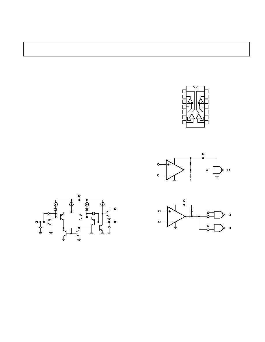
PIN CONNECTIONS
14-Lead Cerdip
14-Lead Plastic DIP
14-Lead SOIC
14
13
12
11
10
9
8
1
2
3
4
5
6
7
CMP04
1
4
3
2
OUT 2
OUT 3
OUT 1
V+
IN 1
IN 1+
IN 2
IN 2+
OUT 4
GND
IN 4+
IN 4
IN 3+
IN 3
Q3
Q2
100 A
3.5 A
3.5 A
100 A
Q8
+INPUT
*
OUTPUT
Q4
Q7
*
INPUT
Q6
Q5
Q1
V+
*
SUBSTRATE DIODES
Figure 1. Simplified Schematic (1/4 CMP04)
TYPICAL INTERFACE
5.0
1/4
CMP04
3
12
100k
1/4
CD4011
Figure 2a. Driving CMOS
5.0
1/4
CMP04
3
12
10k
1/4 SN7400
Figure 2b. Driving TTL
FEATURES
High Gain: 200 V/mV typ
Single or Dual Supply Operation
Input Voltage Range Includes Ground
Low Power Consumption (1.5 mW/Comparator)
Low Input Bias Current: 100 nA max
Low Input Offset Current: 10 nA max
Low Offset Voltage: 1 mV max
Low Output Saturation Voltage: 250 mV @ 4 mA
Logic Output Compatible with TTL, DTL, ECL, MOS and
CMOS
Directly Replaces LM139/239/339 Comparators
Available in Die Form
One Technology Way, P.O. Box 9106, Norwood, MA 02062-9106, U.S.A.
Tel: 781/329-4700
World Wide Web Site: http://www.analog.com
Fax: 781/326-8703
© Analog Devices, Inc., 1998
REV. C
2
ELECTRICAL CHARACTERISTICS
(@ V+ = +5 V, T
A
= +25 C, unless otherwise noted)
Parameter
Symbol
Conditions
Min
Typ
Max
Units
Input Offset Voltage
V
OS
R
S
= 0
, R
L
= 5.1 k
, V
O
= 1.4 V
1
0.4
1
mV
Input Offset Current
I
OS
I
IN
(+) I
IN
(), R
L
= 5.1 k
, V
O
= 1.4 V
2
10
nA
Input Bias Current
I
B
I
IN
(+) or I
IN
()
25
100
nA
Voltage Gain
A
V
R
L
15 k
, V+ = 15 V
2
80
200
V/mV
Large-Signal Response Time
t
r
V
IN
= TTL Logic Swing, V
REF
= 1.4 V
3
V
RL
= 5 V, R
L
= 5.1 k
300
ns
Small-Signal Response Time
t
r
V
IN
= 100 mV Step
3
, 5 mV Overdrive
V
RL
= 5 V, R
L
= 5.1 k
1.3
µ
s
Input Voltage Range
CMVR
(Note 4)
0
V+ 1.5
V
Common-Mode Rejection Ratio
CMRR
(Notes 2, 5)
80
100
dB
Power Supply Rejection Ratio
PSRR
V+ = +5 V to +18 V
2
80
100
dB
Saturation Voltage
V
OL
V
IN
()
1 V, V
IN
(+) = 0, I
SINK
4 mA
250
400
mV
Output Sink Current
I
SINK
V
IN
()
1 V, V
IN
(+) = 0, V
O
1.5 V
6
16
mA
Output Leakage Current
I
LEAK
V
IN
(+)
1 V, V
IN
() = 0, V
O
= 30 V
0.1
100
nA
Supply Current
I+
R
L
=
, All Comps V+ = 30 V
0.8
2.0
mA
NOTES
1
At output switch point, V
O
= 1.4 V, R
S
= 0
with V+ from 5 V; and over the full input common-mode range (0 V to V+ 1.5 V).
2
Guaranteed by design.
3
Sample tested.
4
The input common-mode voltage or input signal voltage should not be allowed to go negative by more than 0.3 V. The upper end of the common-mode voltage range
is V+ 1.5 V, but either or both inputs can go to +30 V without damage.
5
R
L
15 k
, V+ = 15 V, V
CM
= 1.5 V to 13.5 V.
Specifications subject to change without notice.
CMP04SPECIFICATIONS
ORDERING GUIDE
T
A
= +25 C
Temperature
Package
Package
Model
V
OS
Ranges
Descriptions
Options
CMP04BY/883C
1 mV
55
°
C to +125
°
C
14-Lead Cerdip
Q-14
CMP04FP
1 mV
40
°
C to +85
°
C
14-Lead Plastic DIP
N-14
CMP04FS
1 mV
40
°
C to +85
°
C
14-Lead SOIC
R-14/SO-14
ABSOLUTE MAXIMUM RATINGS
1
Supply Voltage . . . . . . . . . . . . . . . . . . . . . . . . . . 36 V or
±
18 V
Differential Input Voltage . . . . . . . . . . . . . . . . . . . . . . 36 V dc
Input Voltage . . . . . . . . . . . . . . . . . . . . . . . . . 0.3 V to +36 V
Operating Temperature Range
CMP04BY . . . . . . . . . . . . . . . . . . . . . . . . 55
°
C to +125
°
C
CMP04FP, FS . . . . . . . . . . . . . . . . . . . . . . 40
°
C to +85
°
C
Junction Temperature (T
J
) . . . . . . . . . . . . . 65
°
C to +150
°
C
Storage Temperature Range . . . . . . . . . . . . 65
°
C to +150
°
C
(P Suffix) . . . . . . . . . . . . . . . . . . . . . . . . . 65
°
C to +125
°
C
Input Current (V
IN
< 3.0 V) . . . . . . . . . . . . . . . . . . . 50 mA
Output Short-Circuit to GND . . . . . . . . . . . . . . . . Continuous
Lead Temperature (Soldering, 60 sec) . . . . . . . . . . . . +300
°
C
Package Type
JA
2
JC
Units
14-Lead Hermetic DIP (Y)
94
10
°
C/W
14-Lead Plastic DIP (P)
83
39
°
C/W
14-Lead SOIC
120
36
°
C/W
NOTES
1
Absolute maximum ratings apply to both DICE and packaged parts, unless
otherwise noted. Stresses above those listed under Absolute Maximum Ratings
may cause permanent damage to the device. This is a stress rating only; functional
operation of the device at these or any other conditions above those listed in the
operational sections of this specification is not implied. Exposure to absolute
maximum rating conditions for extended periods may affect device reliability.
2
JA
is specified for worst case mounting conditions, i.e.,
JA
is specified for device
in socket for cerdip and plastic DIP packages;
JA
is specified for device soldered
to printed circuit board for SO package.
CAUTION
ESD (electrostatic discharge) sensitive device. Electrostatic charges as high as 4000 V readily
accumulate on the human body and test equipment and can discharge without detection.
Although the CMP04 features proprietary ESD protection circuitry, permanent damage may
occur on devices subjected to high energy electrostatic discharges. Therefore, proper ESD
precautions are recommended to avoid performance degradation or loss of functionality.
WARNING!
ESD SENSITIVE DEVICE
ELECTRICAL CHARACTERISTICS
CMP04B/F
1
Parameter
Symbol
Conditions
Min
Typ
Max
Units
Input Offset Voltage
V
OS
R
S
= 0
, R
L
= 5.1 k
1
2
mV
V
O
= 1.4 V
2
1
2
mV
Input Offset Current
I
OS
I
IN
(+) I
IN
()
4
20
nA
R
L
= 5.1 k
4
20
nA
V
O
= 1.4 V
4
20
nA
Input Bias Current
I
B
I
IN
(+) or I
IN
()
40
200
nA
Voltage Gain
A
V
R
L
15 k
, V+ = 15 V
3
70
125
V/mV
Large-Signal Response Time
t
r
V
IN
= TTL Logic Swing
300
ns
V
REF
= 1.4 V
4
300
ns
V
RL
= 5 V, R
L
= 5.1 k
300
ns
Small-Signal Response Time
t
r
V
IN
= 100 mV Step
4
1.3
µ
s
5 mV Overdrive
1.3
µ
s
V
RL
= 5 V, R
L
= 5.1 k
1.3
µ
s
Input Voltage Range
CMVR
(Note 5)
0
V+ 1.5
V
Common-Mode Rejection Ratio
CMRR
(Notes 1, 3)
60
100
dB
Power Supply Rejection Ratio
PSRR
V+ = +5 V to +18 V
80
100
dB
Saturation Voltage
V
OL
V
IN
()
1 V, V
IN
(+) = 0,
250
700
mV
I
SINK
4 mA
250
700
mV
Output Sink Current
I
SINK
V
IN
()
1 V,
5
16
mA
V
IN
(+) = 0, V
O
1.5 V
5
16
mA
Output Leakage Current
I
LEAK
V
IN
(+)
1 V,
0.1
200
nA
V
IN
() = 0, V
O
= 30 V
0.1
200
nA
Supply Current
I+
R
L
=
, All Comps
1.2
3.0
mA
V+ = 30 V
1.2
3.0
mA
NOTES
1
R
L
15 k
, V+ = 15 V, V
CM
= 1.5 V to 13.5 V.
2
At output switch point, V
O
= 1.4 V, R
S
= 0
with V+ from 5 V; and over the full input common-mode range (0 V to V+ 1.5 V).
3
Guaranteed by design.
4
Sample tested.
5
The input common-mode voltage or input signal voltage should not be allowed to go negative by more than 0.3 V. The upper end of the common-mode
voltage range is V+ 1.5 V, but either or both inputs can go to +30 V without damage.
Specifications subject to change without notice.
(@ V+ = +5 V, 55 C
T
A
+125 C for CMP04BY, 40 C
T
A
+85 C for
CMP04FP/FS, unless otherwise noted)
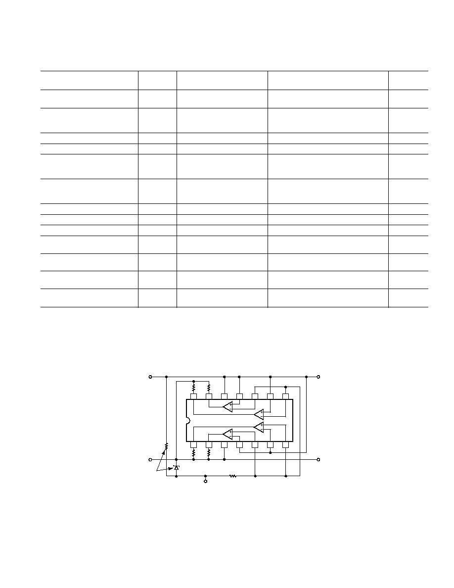
CMP04
3
3.6k
2
3
4
5
6
1
7
13
12
11
10
9
14
8
3.6k
4
2
1
CMP04
3.6k
3.6k
ZENER
5.8V TO 6.2V
1 WATT
470k
+30V
TO ADJACENT SOCKETS
18V
+18V
18V
100k
ONE EACH
PER BOARD
+18V
MIL-STD-883, METHOD 1015, CONDITION B
Figure 3. Burn-In Circuit
3
REV. C
CMP04
4
REV. C
DICE CHARACTERISTICS
WAFER TEST LIMITS
CMP04N
CMP04G
Parameter
Symbol
Conditions
Limit
Limit
Units
Input Offset Voltage
V
OS
R
S
= 0
, R
L
= 5.1 k
V
O
= 1.4 V
1
1
2
mV max
Input Offset Current
I
OS
I
IN
(+) I
IN
()
R
L
= 5.1 k
V
O
= 1.4 V
10
25
nA max
Input Bias Current
I
B
I
IN
(+) or I
IN
()
1
100
100
nA max
Voltage Gain
A
V
R
L
15 k
, V+ = 15 V
3
80
50
V/mV min
Input Voltage Range
CMVR
(Notes 2, 3)
V+ 1.5
V+ 1.5
V max
Common-Mode Rejection Ratio
CMRR
(Note 4)
80
80
dB min
Power Supply Rejection Ratio
PSRR
V+ = +5 V to +18 V
80
80
dB min
Saturation Voltage
V
OL
V
IN
()
1 V, V
IN
(+) = 0,
I
SINK
4 mA
400
400
mV max
Output Sink Current
I
SINK
V
IN
()
1 V,
V
IN
(+) = 0, V
O
1.5 V
6
6
mA min
Output Leakage Current
I
LEAK
V
IN
(+)
1 V,
V
IN
() = 0, V
O
= 30 V
100
100
nA max
Supply Current
I+
R
L
=
, All Comps
V+ = 30 V
2
2
mA max
NOTES
Electrical tests are performed at wafer probe to the limits shown. Due to variations in assembly methods and normal yield loss, yield after packaging is not guaranteed
for standard product dice. Consult factory to negotiate specifications based on dice lot qualification through sample lot assembly and testing.
(@ V+ = +5 V, T
A
= +25 C, unless otherwise noted)
TYPICAL ELECTRICAL CHARACTERISTICS
.
CMP04N
CMP04G
Parameter
Symbol
Conditions
Typical
Typical
Units
Large-Signal Response Time
t
r
V
IN
= TTL Logic Swing
V
REF
= 1.4 V
5
V
RL
= 5 V, R
L
= 5.1 k
600
600
ns
Small-Signal Response Time
t
r
V
IN
= 100 mV Step
5
5 mV Overdrive
V
RL
= 5 V, R
L
= 5.1 k
1.3
1.3
µ
s
(@ V+ = +5 V, unless otherwise noted)
NOTES
1
At output switch point, V
O
= 1.4 V, R
S
= 0
with V+ from 5 V; and over the
full input common-mode range (0 V to V+ 1.5 V).
2
The input common-mode voltage or either input signal voltage should not be allowed
to go negative by more than 0.3 V. The upper end of the common-mode voltage
range is V+ 1.5 V, but either or both inputs can go to +30 V without damage.
3
Guaranteed by design.
4
R
L
15 k
. V
CM
= 1.5 V to 13.5 V.
5
Sample tested.
Specifications subject to change without notice.
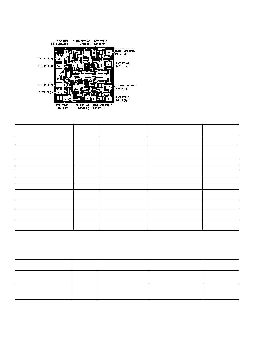
DIE SIZE 0.058
×
0.055 inch, 3190 sq. mils
(1.47
×
1.40 mm, 2.058 sq. mm)
CMP04
5
REV. C
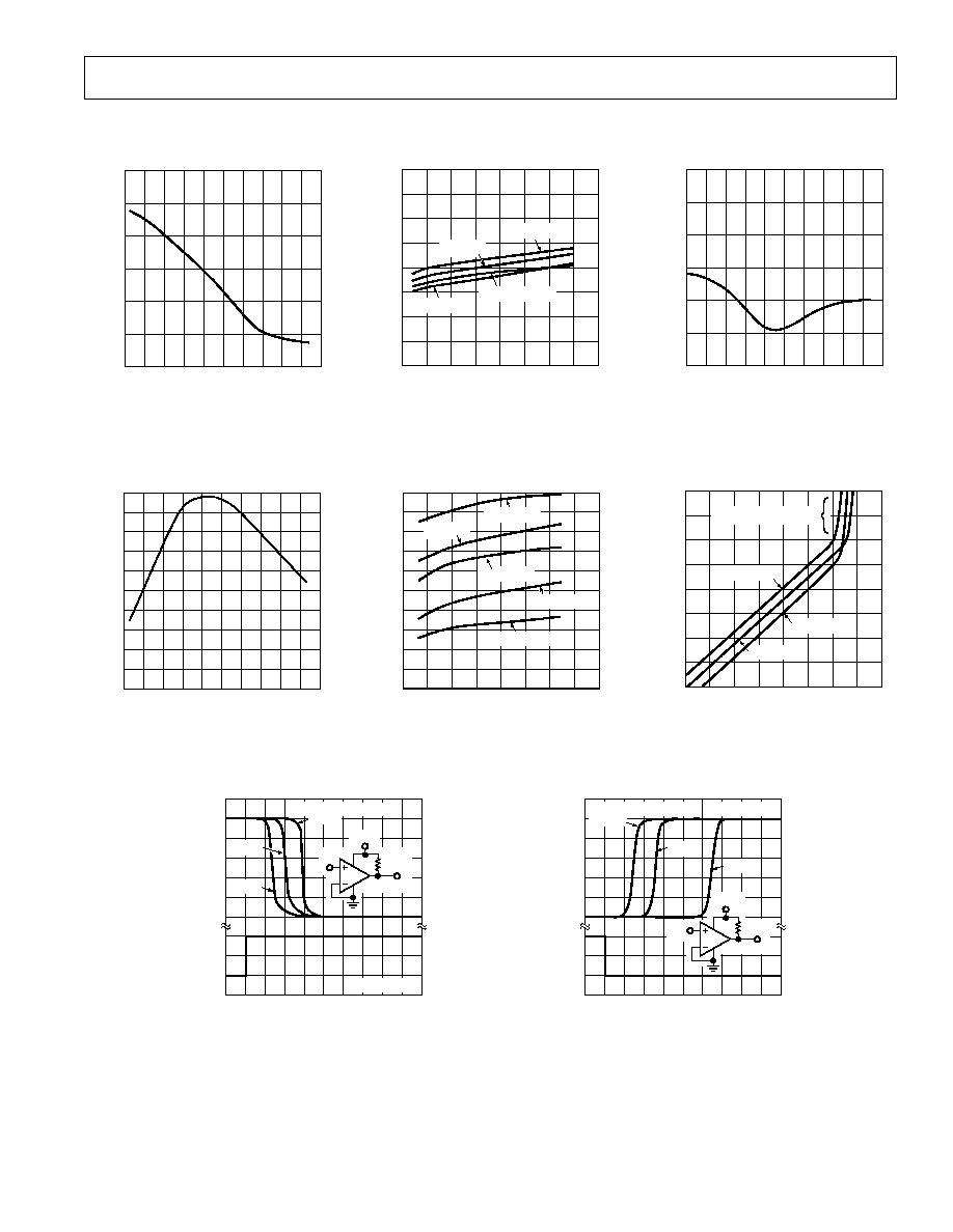
TEMPERATURE C
V
OS
OFFSET VOLTAGE mV
+0.3
40
0
+0.2
+0.1
0
0.1
0.2
0.3
20
20
40
60
80 100 120 140
60
Figure 4. Offset Voltage vs.
Temperature
TEMPERATURE C
A
V
VOLTAGE GAIN V/
mV
160
40
0
110
100
90
80
70
60
20
20
40
60
80 100 120 140
60
150
140
130
120
Figure 7. Voltage Gain vs.
Temperature
Typical Performance Characteristics
V+ SUPPLY VOLTAGE V
DC
I
B
INPUT BIAS CURRENT nA
80
5
15
60
40
20
0
10
20
25
30
35
40
0
T
A
= 0 C
T
A
= +25 C/70 C
T
A
= +125 C
T
A
= 55 C
Figure 5. Input Bias Current vs. V+
and Temperature
SUPPLY VOLTAGE V
DC
1.1
5
15
0.9
0.3
0.1
10
20
25
30
35
40
0
T
A
= 0 C
T
A
= +25 C
T
A
= +125 C
SUPPLY CURRENT mA
0.5
0.7
T
A
= +70 C
T
A
= 55 C
Figure 8. Supply Current vs. Supply
Voltage
TEMPERATURE C
I
OS
INPUT OFFSET CURRENT nA
3.0
40
0
2.0
1.0
0
1.0
2.0
3.0
20
20
40
60
80 100 120 140
60
Figure 6. Input Offset Current vs.
Temperature
I
O
OUTPUT SINK CURRENT mA
V
OL
SATURATION VOLTAGE V
DC
10
1.0
0.1
0.01
0.001
0.1
1.0
10
100
0.01
T
A
= +25 C
T
A
= 55 C
OUT OF SATURATION
T
A
= +125 C
Figure 9. Output Voltage vs. Out-
put Current and Temperature
TIME s
6.0
5.0
50
100
0.5
1.0
1.5
2.0
0
20mV
T
A
= +25 C
OUTPUT VOLTAGE
V
O
Volts
0
4.0
3.0
2.0
1.0
0
INPUT VOLTAGE
V
IN
mV
100mV
INPUT OVERDRIVE =
5.0mV
V
IN
5.1k
V
OUT
+5V
DC
Figure 10. Response Time for Various Input
Overdrives--Negative Transition
TIME s
6.0
5.0
50
100
0.5
1.0
1.5
2.0
0
20mV
T
A
= +25 C
OUTPUT VOLTAGE
V
O
Volts
0
4.0
3.0
2.0
1.0
0
INPUT VOLTAGE
V
IN
mV
5mV
INPUT OVERDRIVE =
100mV
V
IN
5.1k
V
OUT
+5V
DC
Figure 11. Response Time for Various Input
Overdrives--Positive Transition