 | ÐлекÑÑоннÑй компоненÑ: CMP04FP | СкаÑаÑÑ:  PDF PDF  ZIP ZIP |
Äîêóìåíòàöèÿ è îïèñàíèÿ www.docs.chipfind.ru
REV. D
a
CMP04
Information furnished by Analog Devices is believed to be accurate and
reliable. However, no responsibility is assumed by Analog Devices for its
use, nor for any infringements of patents or other rights of third parties that
may result from its use. No license is granted by implication or otherwise
under any patent or patent rights of Analog Devices. Trademarks and
registered trademarks are the property of their respective companies.
One Technology Way, P.O. Box 9106, Norwood, MA 02062-9106, U.S.A.
Tel: 781/329-4700
www.analog.com
Fax: 781/326-8703
© 2003 Analog Devices, Inc. All rights reserved.
Quad Low Power,
Precision Comparator
FEATURES
High Gain: 200 V/mV Typ
Single- or Dual-Supply Operation
Input Voltage Range Includes Ground
Low Power Consumption (1.5 mW/Comparator)
Low Input Bias Current: 100 nA Max
Low Input Offset Current: 10 nA Max
Low Offset Voltage: 1 mV Max
Low Output Saturation Voltage: 250 mV @ 4 mA
Logic Output Compatible with TTL, DTL, ECL, MOS,
and CMOS
Directly Replaces LM139/LM239/LM339 Comparators
GENERAL DESCRIPTION
Four precision independent comparators comprise the CMP04.
Performance highlights include a very low offset voltage, low
output saturation voltage, and high gain in a single-supply
design. The input voltage range includes ground for single-
supply operation and V for split supplies. A low power
supply current of 2 mA, which is independent of supply voltage,
makes this the preferred comparator for precision applications
requiring minimal power consumption. Maximum logic inter-
face flexibility is offered by the open-collector TTL output.
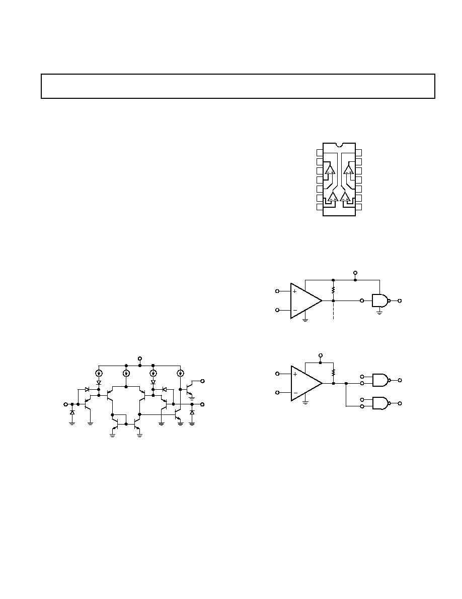
Q3
Q2
100 A
3.5 A
3.5 A
100 A
Q8
+INPUT
*
OUTPUT
Q4
Q7
*
INPUT
Q6
Q5
Q1
V+
*SUBSTRATE DIODES
Figure 1. Simplified Schematic (1/4 CMP04)
PIN CONNECTIONS
14-Lead SOIC
14
13
12
11
10
9
8
1
2
3
4
5
6
7
CMP04
1
4
3
2
OUT 2
OUT 3
OUT 1
V+
IN 1
IN 1+
IN 2
IN 2+
OUT 4
GND
IN 4+
IN 4
IN 3+
IN 3
TYPICAL INTERFACE
5.0
1/4
CMP04
3
12
100k
1/4
CD4011
Figure 2a. Driving CMOS
5.0
1/4
CMP04
3
12
10k
1/4 SN7400
Figure 2b. Driving TTL
REV. D
2
CMP04SPECIFICATIONS
Parameter
Symbol
Conditions
Min
Typ
Max
Unit
Input Offset Voltage
V
OS
R
S
= 0
, R
L
= 5.1 k
, V
O
= 1.4 V
1
0.4
1
mV
Input Offset Current
I
OS
I
IN
(+) I
IN
(), R
L
= 5.1 k
, V
O
= 1.4 V
2
10
nA
Input Bias Current
I
B
I
IN
(+) or I
IN
()
25
100
nA
Voltage Gain
A
V
R
L
15 k, V+ = 15 V
2
80
200
V/mV
Large Signal Response Time
t
r
V
IN
= TTL Logic Swing, V
REF
= 1.4 V
3
V
RL
= 5 V, R
L
= 5.1 k
300
ns
Small Signal Response Time
t
r
V
IN
= 100 mV Step
3
, 5 mV Overdrive
V
RL
= 5 V, R
L
= 5.1 k
1.3
µs
Input Voltage Range
CMVR
Note 4
0
V+ 1.5
V
Common-Mode Rejection Ratio
CMRR
Notes 2, 5
80
100
dB
Power Supply Rejection Ratio
PSRR
V+ = 5 V to 18 V
2
80
100
dB
Saturation Voltage
V
OL
V
IN
()
1 V, V
IN
(+) = 0, I
SINK
4 mA
250
400
mV
Output Sink Current
I
SINK
V
IN
()
1 V, V
IN
(+) = 0, V
O
1.5 V
6
16
mA
Output Leakage Current
I
LEAK
V
IN
(+)
1 V, V
IN
() = 0, V
O
= 30 V
0.1
100
nA
Supply Current
I+
R
L
=
, All Comps V+ = 30 V
0.8
2.0
mA
NOTES
1
At output switch point, V
O
= 1.4 V, R
S
= 0
with V+ from 5 V, and over the full input common-mode range (0 V to V+ 1.5 V).
2
Guaranteed by design.
3
Sample tested.
4
The input common-mode voltage or input signal voltage should not be allowed to go negative by more than 0.3 V. The upper end of the common-mode voltage range
is V+ 1.5 V, but either or both inputs can go to 30 V without damage.
5
R
L
15 k, V+ = 15 V, V
CM
= 1.5 V to 13.5 V.
Specifications subject to change without notice.
ELECTRICAL CHARACTERISTICS
(@ V+ = 5 V, T
A
= 25 C, unless otherwise noted.)
ABSOLUTE MAXIMUM RATINGS
1
Supply Voltage . . . . . . . . . . . . . . . . . . . . . . . . +36 V or
±18 V
Differential Input Voltage . . . . . . . . . . . . . . . . . . . . . . 36 V dc
Input Voltage . . . . . . . . . . . . . . . . . . . . . . . . . 0.3 V to +36 V
Operating Temperature Range
CMP04FS . . . . . . . . . . . . . . . . . . . . . . . . . 40
°C to +85°C
Junction Temperature (T
J
) . . . . . . . . . . . . . 65
°C to +150°C
Storage Temperature Range . . . . . . . . . . . . 65
°C to +150°C
Input Current (V
IN
< 3.0 V) . . . . . . . . . . . . . . . . . . . 50 mA
Output Short Circuit to GND . . . . . . . . . . . . . . . . Continuous
Lead Temperature (Soldering, 60 sec) . . . . . . . . . . . . . 300
°C
Package Type
JA
2
JC
Unit
14-Lead SOIC
120
36
°C/W
NOTES
1
Absolute maximum ratings apply to both DICE and packaged parts, unless
otherwise noted. Stresses above those listed under Absolute Maximum Ratings
may cause permanent damage to the device. This is a stress rating only; functional
operation of the device at these or any other conditions above those listed in the
operational sections of this specification is not implied. Exposure to absolute
maximum rating conditions for extended periods may affect device reliability.
2
JA
is specified for worst-case mounting conditions, i.e.,
JA
is specified for device
soldered to printed circuit board for SOIC package.
ORDERING GUIDE
T
A
= 25 C
Temperature
Package
Package
Model
V
OS
Ranges
Descriptions
Options
CMP04FS
1 mV
40
°C to +85°C
14-Lead SOIC
R-14
CAUTION
ESD (electrostatic discharge) sensitive device. Electrostatic charges as high as 4000 V readily
accumulate on the human body and test equipment and can discharge without detection. Although
the CMP04 features proprietary ESD protection circuitry, permanent damage may occur on
devices subjected to high energy electrostatic discharges. Therefore, proper ESD precautions are
recommended to avoid performance degradation or loss of functionality.
WARNING!
ESD SENSITIVE DEVICE
REV. D
3
CMP04
CMP04F
1
Parameter
Symbol
Conditions
Min
Typ
Max
Unit
Input Offset Voltage
V
OS
R
S
= 0
, R
L
= 5.1 k
1
2
mV
V
O
= 1.4 V
2
1
2
mV
Input Offset Current
I
OS
I
IN
(+) I
IN
()
4
20
nA
R
L
= 5.1 k
4
20
nA
V
O
= 1.4 V
4
20
nA
Input Bias Current
I
B
I
IN
(+) or I
IN
()
40
200
nA
Voltage Gain
A
V
R
L
15 k, V+ = 15 V
3
70
125
V/mV
Large Signal Response Time
t
r
V
IN
= TTL Logic Swing
300
ns
V
REF
= 1.4 V
4
300
ns
V
RL
= 5 V, R
L
= 5.1 k
300
ns
Small Signal Response Time
t
r
V
IN
= 100 mV Step
4
1.3
µs
5 mV Overdrive
1.3
µs
V
RL
= 5 V, R
L
= 5.1 k
1.3
µs
Input Voltage Range
CMVR
Note 5
0
V+ 1.5
V
Common-Mode Rejection Ratio
CMRR
Notes 1, 3
60
100
dB
Power Supply Rejection Ratio
PSRR
V+ = 5 V to 18 V
80
100
dB
Saturation Voltage
V
OL
V
IN
()
1 V, V
IN
(+) = 0,
250
700
mV
I
SINK
4 mA
250
700
mV
Output Sink Current
I
SINK
V
IN
()
1 V,
5
16
mA
V
IN
(+) = 0, V
O
1.5 V
5
16
mA
Output Leakage Current
I
LEAK
V
IN
(+)
1 V,
0.1
200
nA
V
IN
() = 0, V
O
= 30 V
0.1
200
nA
Supply Current
I+
R
L
=
, All Comps
1.2
3.0
mA
V+ = 30 V
1.2
3.0
mA
NOTES
1
R
L
15 k, V+ = 15 V, V
CM
= 1.5 V to 13.5 V.
2
At output switch point, V
O
= 1.4 V, R
S
= 0
with V+ from 5 V; and over the full input common-mode range (0 V to V+ 1.5 V).
3
Guaranteed by design.
4
Sample tested.
5
The input common-mode voltage or input signal voltage should not be allowed to go negative by more than 0.3 V. The upper end of the common-mode
voltage range is V+ 1.5 V, but either or both inputs can go to +30 V without damage.
Specifications subject to change without notice.
ELECTRICAL CHARACTERISTICS
(@ V+ = 5 V, 40 C
T
A
+85 C for CMP04FS, unless otherwise noted.)
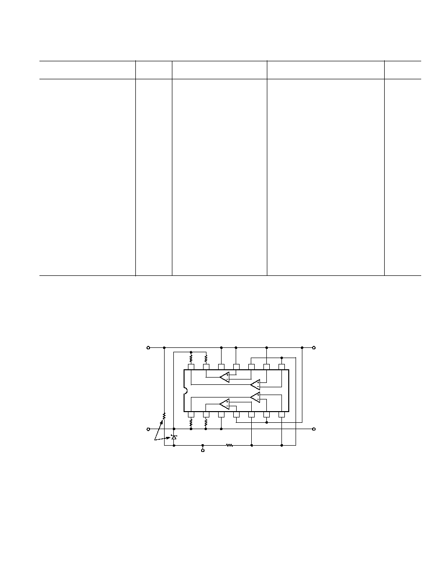
3
3.6k
2
3
4
5
6
1
7
13
12
11
10
9
14
8
3.6k
4
2
1
CMP04
3.6k
3.6k
ZENER
5.8V TO 6.2V
1 WATT
470k
30V
TO ADJACENT SOCKETS
18V
+18V
18V
100k
ONE EACH
PER BOARD
+18V
MIL-STD-883, METHOD 1015, CONDITION B
Figure 3. Burn-In Circuit
REV. D
4
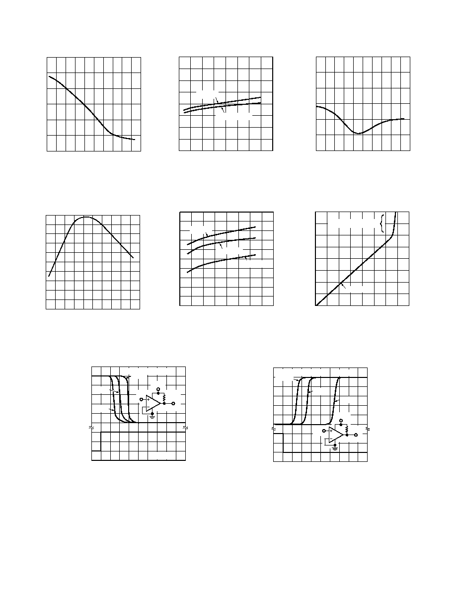
CMP04Typical Performance Characteristics
TEMPERATURE ( C)
V
OS
OFFSET VOLTAGE (mV)
0.3
40
0
0.2
0.1
0
0.1
0.2
0.3
20
20
40
60
80 100 120 140
60
TPC 1. Offset Voltage vs.
Temperature
TEMPERATURE ( C)
A
V
VOLTAGE GAIN (V/
mV)
160
40
0
110
100
90
80
70
60
20
20
40
60
80 100 120 140
60
150
140
130
120
TPC 4. Voltage Gain vs.
Temperature
V+ SUPPLY VOLTAGE (V
DC
)
I
B
INPUT BIAS CURRENT (nA)
80
5
15
60
40
20
0
10
20
25
30
35
40
0
T
A
= 0 C
T
A
= +25 C/70 C
TPC 2. Input Bias Current vs. V+
and Temperature
SUPPLY VOLTAGE (V
DC
)
1.1
5
15
0.9
0.3
0.1
10
20
25
30
35
40
0
T
A
= 0 C
T
A
= +25 C
SUPPLY CURRENT (mA)
0.5
0.7
T
A
= +70 C
TPC 5. Supply Current vs. Supply
Voltage
TEMPERATURE ( C)
I
OS
INPUT OFFSET CURRENT (nA)
3.0
40
0
2.0
1.0
0
1.0
2.0
3.0
20
20
40
60
80 100 120 140
60
TPC 3. Input Offset Current vs.
Temperature
I
O
OUTPUT SINK CURRENT (mA)
V
OL
SATURATION VOLTAGE (V
DC
)
10
1.0
0.1
0.01
0.001
0.1
1.0
10
100
0.01
T
A
= +25 C
OUT OF SATURATION
TPC 6. Output Voltage vs. Output
Current and Temperature
TIME ( s)
6.0
5.0
50
100
0.5
1.0
1.5
2.0
0
20mV
T
A
= 25 C
OUTPUT VOLTAGE
V
O
(V)
0
4.0
3.0
2.0
1.0
0
INPUT VOLTAGE
V
IN
(mV)
100mV
INPUT OVERDRIVE =
5.0mV
V
IN
5.1k
V
OUT
5V
DC
TPC 7. Response Time for Various Input
Overdrives--Negative Transition
TIME ( s)
6.0
5.0
50
100
0.5
1.0
1.5
2.0
0
20mV
T
A
= 25 C
OUTPUT VOLTAGE
V
O
(V)
0
4.0
3.0
2.0
1.0
0
INPUT VOLTAGE
V
IN
(mV)
5mV
INPUT OVERDRIVE =
100mV
V
IN
5.1k
V
OUT
5V
DC
TPC 8. Response Time for Various Input
Overdrives--Positive Transition
REV. D
CMP04
5
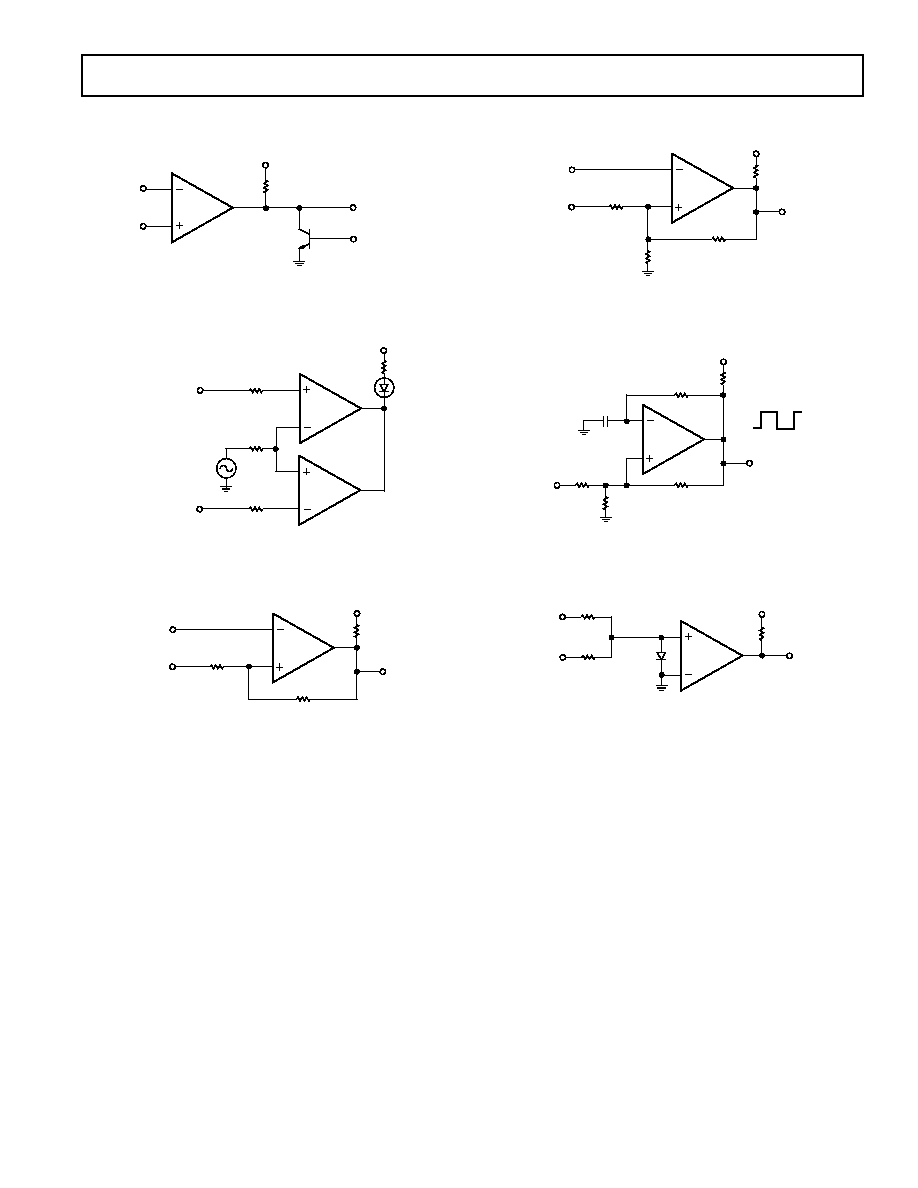
TYPICAL APPLICATIONS
V+
1/4
CMP04
6.2k
V
O
STROBE
INPUT
*
*
OR LOGIC WITHOUT
PULLUP RESISTOR
Figure 4. Output Strobing
R
S
+V
REF
HIGH
1/4
CMP04
1/4
CMP04
+V
REF
LOW
2R
S
2R
S
+V
IN
Figure 5. Limit Comparator
10k
+V
REF
1/4
CMP04
+V
IN
V
O
10M
3k
V+
Figure 6. Noninverting Comparator with Hysteresis
1M
V+
1/4
CMP04
+V
IN
V
O
1M
3k
V+
1M
Figure 7. Inverting Comparator with Hysteresis
100k
V+
1/4
CMP04
V
O
100k
4.3k
V+
100k
V+
0
f = 186kHz
75pF
100k
Figure 8. Square Wave Oscillator
1N914
1/4
CMP04
V
O
5.1k
V+
100k
V
IN1
100k
V
IN2
Figure 9. Comparing Input Voltages of Opposite Polarity
Document Outline
- FEATURES
- GENERAL DESCRIPTION
- PIN CONNECTIONS
- TYPICAL INTERFACE
- SPECIFICATIONS
- ABSOLUTE MAXIMUM RATINGS
- ORDERING GUIDE
- ELECTRICAL CHARACTERISTICS
- Typical Performance Characteristics
- TYPICAL APPLICATIONS
- OUTLINE DIMENSIONS
- Revision History