 | ÐлекÑÑоннÑй компоненÑ: OP186 | СкаÑаÑÑ:  PDF PDF  ZIP ZIP |
Äîêóìåíòàöèÿ è îïèñàíèÿ www.docs.chipfind.ru

REV. 0
Information furnished by Analog Devices is believed to be accurate and
reliable. However, no responsibility is assumed by Analog Devices for its
use, nor for any infringements of patents or other rights of third parties
which may result from its use. No license is granted by implication or
otherwise under any patent or patent rights of Analog Devices.
a
OP186
One Technology Way, P.O. Box 9106, Norwood, MA 02062-9106, U.S.A.
Tel: 781/329-4700
World Wide Web Site: http://www.analog.com
Fax: 781/326-8703
© Analog Devices, Inc., 1998
5 A, Rail-to-Rail
Output Operational Amplifier
FUNCTIONAL BLOCK DIAGRAM
5-Lead SOT-23
(RT Suffix)
TOP VIEW
(Not to Scale)
5
4
1
2
3
OUT
V+
+IN
V
IN
OP186
FEATURES
Low Supply Current: 5.5 A max
Single-Supply Operation: 2.2 V to 12 V
Wide Bandwidth: 160 kHz
Wide Input Voltage Range
Rail-to-Rail Output Swing
No Phase Reversal
Output Short Circuit Current: 10 mA
APPLICATIONS
Portable Phones
Comparator
Battery Powered Instrumentation
Safety Monitoring
Remote Sensors
Low Voltage Strain Gauge Amplifiers
GENERAL DESCRIPTION
The OP186 is a single, low voltage, ultralow power single-
supply, amplifier featuring rail-to-rail outputs. Specifications are
guaranteed at +2.2 V, +2.7 V, and +5.0 V single supply as well
as
±
5 V dual supplies.
Fabricated on Analog Device's CBCMOS process, the OP186
features a bipolar input and an output that swings to within
millivolts of the supplies while continuing to sink or source
current all the way to the supplies.
Applications for these amplifiers include safety monitoring,
portable equipment, battery and power supply control, and as
signal conditioning and interface for transducers in very low
power systems.
The output's ability to swing rail-to-rail and not increase supply
current when the output is driven to a supply enables the
OP186 to be used as a comparator in very low power systems.
The OP186 is specified over the extended industrial (40
°
C to
+125
°
C) temperature range. The OP186 is available in the
SOT-23-5 package.

2
REV. 0
OP186SPECIFICATIONS
ELECTRICAL CHARACTERISTICS
Parameter
Symbol
Conditions
Min
Typ
Max
Units
INPUT CHARACTERISTICS
Offset Voltage
V
OS
1
0.8
5
mV
0
°
C
T
A
+125
°
C
6
mV
Input Bias Current
I
B
3
7
nA
0
°
C
T
A
+125
°
C
10
nA
Input Offset Current
I
OS
0.1
2
nA
0
°
C
T
A
+125
°
C
5
nA
Input Voltage Range
V
CM
0
1.2
V
Common-Mode Rejection Ratio
CMRR
V
CM
= 0 V to 1.2 V
65
90
dB
0
°
C
T
A
+125
°
C
60
dB
Large Signal Voltage Gain
A
VO
R
L
= 1 M
, V
O
= 0.3 V to 1.9 V
5
18
V/mV
0
°
C
T
A
+125
°
C
2
V/mV
Offset Voltage Drift
V
OS
/
T
3.5
µ
V/
°
C
Bias Current Drift
I
B
/
T
30
pA/
°
C
Offset Current Drift
I
OS
/
T
3
pA/
°
C
OUTPUT CHARACTERISTICS
Output Voltage High
V
OH
R
L
= 100 k
to GND
2.125
2.16
V
0
°
C to +125
°
C
2.1
V
Output Voltage Low
V
OL
R
L
= 100 k
to V+
25
60
mV
0
°
C to +125
°
C
75
mV
Short Circuit Limit
I
SC
±
500
µ
A
POWER SUPPLY
Power Supply Rejection Ratio
PSRR
V
S
= 2.2 V to 12 V
78
95
dB
0
°
C
T
A
+125
°
C
76
dB
Supply Current/Amplifier
I
SY
4
5
µ
A
0
°
C
T
A
+125
°
C
5.5
µ
A
DYNAMIC PERFORMANCE
Slew Rate
SR
R
L
= 100 k
, C
L
= 15 pF
60
V/ms
Turn-On Time
A
V
= 1, V
O
= 1
17
µ
s
A
V
= 20, V
O
= 1
35
µ
s
Gain Bandwidth Product
GBP
150
kHz
Phase Margin
o
60
Degrees
NOISE PERFORMANCE
Voltage Noise Density
e
n
f = 1 kHz
80
nV/
Hz
Current Noise Density
i
n
<1
pA/
Hz
NOTE
1
V
OS
is tested under a no load condition.
Specifications subject to change without notice.
(V
S
= +2.2 V, V
CM
= +1.1 V, T
A
= +25 C unless otherwise noted)

3
REV. 0
OP186
ELECTRICAL CHARACTERISTICS
Parameter
Symbol
Conditions
Min
Typ
Max
Units
INPUT CHARACTERISTICS
Offset Voltage
V
OS
2
0.6
5
mV
40
°
C
T
A
+125
°
C
6
mV
Input Bias Current
I
B
3
7
nA
40
°
C
T
A
+125
°
C
10
nA
Input Offset Current
I
OS
0.1
2
nA
40
°
C
T
A
+125
°
C
5
nA
Input Voltage Range
V
CM
0
1.7
V
Common-Mode Rejection Ratio
CMRR
V
CM
= 0 V to 1.7 V
65
90
dB
40
°
C
T
A
+125
°
C
60
dB
Large Signal Voltage Gain
A
VO
R
L
= 1 M
, V
O
= 0.3 V to 2.4 V
5
22
V/mV
40
°
C
T
A
+125
°
C
2
V/mV
Offset Voltage Drift
V
OS
/
T
3.5
µ
V/
°
C
Bias Current Drift
I
B
/
T
30
pA/
°
C
Offset Current Drift
I
OS
/
T
3
pA/
°
C
OUTPUT CHARACTERISTICS
Output Voltage High
V
OH
R
L
= 100 k
to GND
2.625
2.665
V
40
°
C to +125
°
C
2.6
V
Output Voltage Low
V
OL
R
L
= 100 k
to V+
22
50
mV
40
°
C to +125
°
C
75
mV
Short Circuit Limit
I
SC
±
0.8
mA
POWER SUPPLY
Power Supply Rejection Ratio
PSRR
V
S
= 2.7 V to 12 V
78
95
dB
40
°
C
T
A
+125
°
C
76
dB
Supply Current/Amplifier
I
SY
4.2
5.5
µ
A
40
°
C
T
A
+125
°
C
7
µ
A
DYNAMIC PERFORMANCE
Slew Rate
SR
R
L
=100 k
, C
L
= 15 pF
61
V/ms
Turn-On Time
A
V
= 1, V
O
= 1
17
µ
s
A
V
= 20, V
O
= 1
25
µ
s
Gain Bandwidth Product
GBP
155
kHz
Phase Margin
o
59
Degrees
NOISE PERFORMANCE
Voltage Noise Density
e
n
f = 1 kHz
80
nV/
Hz
Current Noise Density
i
n
<1
pA/
Hz
NOTES
1
+2.7 V specifications are guaranteed by +2.2 V and
±
5 V testing.
2
V
OS
is tested under a no load condition.
Specifications subject to change without notice.
(V
S
= +2.7 V, V
CM
= +1.35 V, T
A
= +25 C unless otherwise noted)
1

4
REV. 0
OP186SPECIFICATIONS
ELECTRICAL CHARACTERISTICS
Parameter
Symbol
Conditions
Min
Typ
Max
Units
INPUT CHARACTERISTICS
Offset Voltage
V
OS
2
0.6
5
mV
40
°
C
T
A
+125
°
C
6
mV
Input Bias Current
I
B
3
7
nA
40
°
C
T
A
+125
°
C
10
nA
Input Offset Current
I
OS
0.1
2
nA
40
°
C
T
A
+125
°
C
5
nA
Input Voltage Range
V
CM
0
4
V
Common-Mode Rejection Ratio
CMRR
V
CM
= 0 V to 4.0 V
65
90
dB
40
°
C
T
A
+125
°
C
60
dB
Large Signal Voltage Gain
A
VO
R
L
= 1 M
, V
O
= 0.5 V to 4.5 V
5
40
V/mV
40
°
C
T
A
+125
°
C
2
V/mV
Offset Voltage Drift
V
OS
/
T
40
°
C
T
A
+125
°
C
3.3
µ
V/
°
C
Bias Current Drift
I
B
/
T
25
pA/
°
C
Offset Current Drift
I
OS
/
T
3
pA/
°
C
OUTPUT CHARACTERISTICS
Output Voltage High
V
OH
R
L
= 100 k
to GND
4.925
4.965
V
40
°
C
T
A
+125
°
C
4.9
V
Output Voltage Low
V
OL
R
L
= 100 k
to V+
20
50
mV
40
°
C
T
A
+125
°
C
75
mV
Short Circuit Limit
I
SC
±
3.5
mA
POWER SUPPLY
Power Supply Rejection Ratio
PSRR
V
S
= 2.7 V to 12 V
78
95
dB
40
°
C
T
A
+125
°
C
76
dB
Supply Current/Amplifier
I
SY
4.7
6
µ
A
40
°
C
T
A
+125
°
C
7.5
µ
A
DYNAMIC PERFORMANCE
Slew Rate
SR
R
L
= 100 k
, C
L
= 15 pF
62
V/ms
Gain Bandwidth Product
GBP
155
kHz
Phase Margin
o
59
Degrees
Saturation Recovery Time
60
µ
s
NOISE PERFORMANCE
Voltage Noise
e
n
p-p
0.1 Hz to 10 Hz
6
µ
V p-p
Voltage Noise Density
e
n
f = 1 kHz
80
nV/
Hz
f = 10 kHz
70
nV/
Hz
Current Noise Density
i
n
<1
pA/
Hz
NOTES
1
+5 V specifications are guaranteed by +2.2 V and
±
5 V testing.
2
V
OS
is tested under a no load condition.
Specifications subject to change without notice.
(V
S
= +5.0 V, V
CM
= +2.5 V, T
A
= +25 C unless otherwise noted)
1

5
REV. 0
OP186
ELECTRICAL CHARACTERISTICS
Parameter
Symbol
Conditions
Min
Typ
Max
Units
INPUT CHARACTERISTICS
Offset Voltage
V
OS
1
0.6
5
mV
40
°
C
T
A
+125
°
C
6
mV
Input Bias Current
I
B
3
7
nA
40
°
C
T
A
+125
°
C
10
nA
Input Offset Current
I
OS
0.1
2
nA
40
°
C
T
A
+125
°
C
5
nA
Input Voltage Range
V
CM
5
+4
V
Common-Mode Rejection
CMRR
V
CM
= 5.0 V to +4.0 V
65
90
dB
40
°
C
T
A
+125
°
C
60
dB
Large Signal Voltage Gain
A
VO
R
L
= 1 M
, V
O
=
±
4.0 V,
50
250
V/mV
40
°
C
T
A
+125
°
C
10
V/mV
Offset Voltage Drift
V
OS
/
T
3
µ
V/
°
C
Bias Current Drift
I
B
/
T
25
pA/
°
C
Offset Current Drift
I
OS
/
T
3
pA/
°
C
OUTPUT CHARACTERISTICS
Output Voltage Swing
V
O
R
L
= 100 k
to GND
±
4.95
±
4.98
V
40
°
C to +125
°
C
±
4.90
V
Short Circuit Limit
I
SC
±
10
mA
POWER SUPPLY
Power Supply Rejection Ratio
PSRR
V
S
=
±
1.35 V to
±
6 V
78
95
dB
40
°
C
T
A
+125
°
C
76
dB
Supply Current/Amplifier
I
SY
V
O
= 0 V
5.2
7
µ
A
40
°
C
T
A
+125
°
C
8
µ
A
DYNAMIC PERFORMANCE
Slew Rate
±
SR
R
L
= 100 k
, C
L
= 15 pF
62
V/ms
Gain Bandwidth Product
GBP
170
kHz
Phase Margin
o
58
Degrees
NOISE PERFORMANCE
Voltage Noise
e
n
p-p
0.1 Hz to 10 Hz
6
µ
V p-p
Voltage Noise Density
e
n
f = 1 kHz
80
nV/
Hz
f = 10 kHz
70
nV/
Hz
Current Noise Density
i
n
<1
pA/
Hz
NOTE
1
V
OS
is tested under a no load condition.
Specifications subject to change without notice.
(V
S
= 5.0 V, T
A
= +25 C unless otherwise noted)
OP186
6
REV. 0
CAUTION
ESD (electrostatic discharge) sensitive device. Electrostatic charges as high as 4000 V readily
accumulate on the human body and test equipment and can discharge without detection.
Although the OP186 features proprietary ESD protection circuitry, permanent damage may
occur on devices subjected to high energy electrostatic discharges. Therefore, proper ESD
precautions are recommended to avoid performance degradation or loss of functionality.
WARNING!
ESD SENSITIVE DEVICE
ABSOLUTE MAXIMUM RATINGS
1
Supply Voltage . . . . . . . . . . . . . . . . . . . . . . . . . . . . . . . . +16 V
Input Voltage . . . . . . . . . . . . . . . . . . . . . . . GND to V
S
+ 10 V
Differential Input Voltage
2
. . . . . . . . . . . . . . . . . . . . . .
±
3.5 V
Output Short-Circuit Duration to GND . . . . . . . . . Indefinite
Storage Temperature Range
RT Package . . . . . . . . . . . . . . . . . . . . . . . 65
°
C to +150
°
C
Operating Temperature Range
OP186G . . . . . . . . . . . . . . . . . . . . . . . . . . 40
°
C to +125
°
C
Junction Temperature Range
RT Package . . . . . . . . . . . . . . . . . . . . . . . 65
°
C to +150
°
C
Lead Temperature Range (Soldering, 60 sec) . . . . . . . +300
°
C
NOTES
1
Stresses above those listed under Absolute Maximum Ratings may cause perma-
nent damage to the device. This is a stress rating only; functional operation of the
device at these or any other conditions above those listed in the operational sections
of this specification is not implied. Exposure to absolute maximum rating condi-
tions for extended periods may affect device reliability.
2
For supplies less than
±
5 V the differential input voltage is limited to the supplies.
ORDERING GUIDE
Temperature
Package
Package
Model
Range
Description
Option
OP186GRT
40
°
C to +125
°
C
5-Lead SOT-23
RT-5
Package Type
JA
1
JC
Units
5-Lead SOT-23 (RT)
230
140
°
C/W
NOTE
1
JA
is specified for worst case conditions, i.e.,
JA
is specified for device in socket
for SOT packages.
OP186
7
REV. 0
INPUT OFFSET VOLTAGE mV
2
45
0
5
40
35
30
25
20
15
10
V
S
= +2.2V
T
A
= +25 C
1.5
1
0.5
0
0.5
1
1.5
2
QUANTITY A
Figure 1. Input Offset Voltage
Distribution
45
0
5
V
S
= 5V
T
A
= +25 C
40
35
30
25
20
15
10
INPUT OFFSET VOLTAGE mV
2
1.5
1
0.5
0
0.5
1
1.5
2
QUANTITY A
Figure 4. Input Offset Voltage
Distribution
INPUT BIAS CURRENT nA
TEMPERATURE C
40
7
6
5
4
3
2
1
0
20
0
20
40
60
80 100 120 140
V
S
= +2.7V
V
S
= 5.5V
Figure 7. Input Bias Current vs.
Temperature
45
0
5
V
S
=
+2.7V
T
A
=
+25 C
40
35
30
25
20
15
10
INPUT OFFSET VOLTAGE mV
2
1.5
1
0.5
0
0.5
1
1.5
2
QUANTITY A
Figure 2. Input Offset Voltage
Distribution
TEMPERATURE C
40
100
50
0
50
100
150
200
250
300
350
20
0
20
40
60
80 100 120 140
V
S
= +2.7V
INPUT OFFSET VOLTAGE
V
V
S
= 5V
V
S
= +2.2V
Figure 5. Input Offset Voltage vs.
Temperature
COMMON-MODE VOLTAGE Volts
4.0
0
0.5
3.5
3.0
2.5
2.0
1.5
1.0
0.5
0
0.5
1.0
1.0 1.5 2.0 2.5 3.0 3.5 4.0 4.5 5.0
V
S
= +5V
T
A
= +25 C
INPUT BIAS CURRENT nA
Figure 8. Input Bias Current vs.
Common-Mode Voltage
45
0
5
V
S
=
+5V
T
A
=
+25 C
40
35
30
25
20
15
10
INPUT OFFSET VOLTAGE mV
2
1.5
1
0.5
0
0.5
1
1.5
2
QUANTITY A
Figure 3. Input Offset Voltage
Distribution
INPUT BIAS CURRENT nA
TEMPERATURE C
40
7
6
5
4
3
2
1
0
20
0
20
40
60
80 100 120 140
V
S
= 5V
V
S
= +2.2V
Figure 6. Input Bias Current vs.
Temperature
INPUT OFFSET CURRENT nA
TEMPERATURE C
40
0.3
0.2
0.1
0
0.1
0.2
0.3
0.4
20
0
20
40
60
80 100 120 140
V
S
= +2.7V, +5V
Figure 9. Input Offset Current vs.
Temperature
Typical Performance Characteristics
OP186
8
REV. 0
LOAD CURRENT A
10
0.1
1
100
1k
1
1000
10
100
V
S
= +2.7V
T
A
= +25 C
SOURCE
SINK
OUTPUT VOLTAGE mV
Figure 10. Output Voltage to Supply
Rail vs. Load Current
FREQUENCY Hz
100
10
0
10
20
30
40
50
60
70
1k
10k
100k
1M
270
225
180
135
90
45
0
V
S
= +2.2V
T
A
= +25 C
R
L
= 100k
OPEN-LOOP GAIN dB
PHASE SHIFT Degrees
PHASE
GAIN
20
30
Figure 13. Open-Loop Gain and
Phase vs. Frequency
0
10
20
30
40
50
FREQUENCY Hz
30
10
20
10
100k
10k
1k
100
1M
CLOSED-LOOP GAIN dB
V
S
= +5V
T
A
= +25 C
R
L
=
Figure 16. Closed-Loop Gain vs.
Frequency
LOAD CURRENT A
10
0.1
1
100
1k
1
1000
10
100
V
S
= +5V
T
A
= +25 C
SOURCE
SINK
OUTPUT VOLTAGE mV
Figure 11. Output Voltage to Supply
Rail vs. Load Current
FREQUENCY Hz
100
30
20
10
0
10
20
30
40
50
60
70
1k
10k
100k
1M
270
225
180
135
90
45
0
V
S
= +5V
T
A
= +25 C
R
L
= 100k
OPEN-LOOP GAIN dB
PHASE SHIFT De
g
rees
GAIN
PHASE
Figure 14. Open-Loop Gain and
Phase vs. Frequency
CMRR dB
FREQUENCY
H
Z
20
40
60
80
100
120
10k
1M
10M
T
A
=
+25 C
100k
1k
+2.7V
V
S
+5V
Figure 17. CMRR vs. Frequency
LOAD CURRENT A
10
0.1
1
100
1k
1
1000
10
100
V
S
= 5V
T
A
= +25 C
SOURCE
SINK
OUTPUT VOLTAGE mV
Figure 12. Output Voltage to Supply
Rail vs. Load Current
FREQUENCY Hz
100
30
20
10
0
10
20
30
40
50
60
70
1k
10k
100k
1M
270
225
180
135
90
45
0
V
S
= 5V
T
A
= +25 C
R
L
= 100k
OPEN-LOOP GAIN dB
PHASE SHIFT Degrees
GAIN
PHASE
Figure 15. Open-Loop Gain and
Phase vs. Frequency
PSRR dB
FREQUENCY Hz
0
10
100
1k
10k
100k
1M
20
40
60
80
100
120
+2.7V V
S
+5V
T
A
= +25 C
R
L
=
`
Figure 18. PSRR vs. Frequency
OP186
9
REV. 0
CAPACITANCE pF
0
10
1000
100
5
10
15
20
25
30
35
40
45
50
55
60
65
V
S
= +5V
V
IN
= 100mV p-p
A
VCL
= +1
R
L
= 100k
T
A
= +25 C
OS
+OS
SMALL SIGNAL OVERSHOOT %
Figure 19. Small Signal Overshoot
vs. Load Capacitance
TEMPERATURE C
40
3
3.5
4
4.5
5
5.5
6.5
20
0
20
40
60
80 100 120 140
6
INPUT BIAS CURRENT nA
V
S
= +2.7V
V
S
= +2.2V
V
S
= 5V
V
S
= 5V
V
S
= +5V
Figure 22. Bias Current vs.
Temperature
500mV
100 s
V
S
= +2.7V
A
V
= +1
R
L
= 100k
C
L
= 50pF
T
A
= +25 C
Figure 25. Large Signal Transient
Response
FREQUENCY Hz
10
2
100
1k
10k
100k
3
0
1
V
S
= +2.7V
V
IN
= 2V p-p
A
VCL
= +1
R
L
=
T
A
= +25 C
MAXIMUM OUTPUT SWING V p-p
Figure 20. Maximum Output Swing
vs. Frequency
SUPPLY VOLTAGE V
6
3
0
0 0.5
5
4
2
1
5.5
4.5
3.5
2.5
1.5
0.5
1 1.5 2 2.5 3 3.5 4 4.5 5 5.5 6
T
A
= +25 C
SUPPLY CURRENT
A
Figure 23. Supply Current vs. Supply
Voltage
1.0V
100 s
V
S
= +5V
A
V
= +1
R
L
= 100k
C
L
= 50pF
T
A
= +25 C
Figure 26. Large Signal Transient
Response
FREQUENCY Hz
5
10
2
100
1k
10k
100k
3
0
1
4
V
S
= +5V
V
IN
= 4V p-p
A
VCL
= +1
R
L
=
T
A
= +25 C
MAXIMUM OUTPUT SWING V p-p
Figure 21. Maximum Output Swing
vs. Frequency
COMMON MODE VOLTAGE V
2
0 0.5
2.25
1 1.5 2 2.5 3 3.5 4 4.5 5 5.5 6
V
S
= +5V
R
L
=
T
A
= +25 C
2.5
2.75
3
3.25
3.5
3.75
4
4.25
4.5
SUPPLY CURRENT
A
Figure 24. Supply Current vs.
Common-Mode Voltage
50mV
100 s
V
S
= 1.35V
A
V
= +1
R
L
= 100k
C
L
= 50pF
T
A
= +25 C
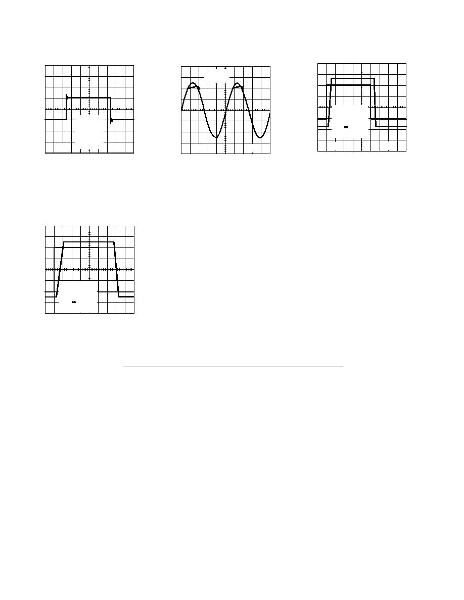
Figure 27. Small Signal Transient
Response
OP186
10
REV. 0
APPLICATIONS
The OP186 is very similar in design to the OP181. Please see the
OP181/OP281/OP481 data sheet for applications information.
Design of the OP186 was based on the OP181. The major dif-
ference is that the trim structures have been removed. This
results in the offset of the OP186 being higher than the OP181.
There are no other major changes to the circuit. Other perfor-
mance differences, such as the higher bandwidth and slightly
higher supply current, also result from the removal of the trim
resistors.
50mV
100 s
V
S
= 2.5V
A
V
= +1
R
L
= 100k
C
L
= 50pF
T
A
= +25 C
Figure 28. Small Signal Transient
Response
100 s
V
S
= 2.5V
A
VOL
= CIRCUIT
V
IN
= 1V p-p
R
L
=
T
A
= +25 C
1.0V
Figure 31. Saturation Recovery Time
1.0V
200 s
V
S
= +5V
T
A
= +25 C
Figure 29. No Phase Reversal
500mV
100 s
V
S
= 1.35V
A
VOL
= CIRCUIT
V
IN
= 1V p-p
R
L
=
T
A
= +25 C
Figure 30. Saturation Recovery Time

OP186
11
REV. 0
SPICE MODEL
* OP186 SPICE Macro-model Typical Values
* 2/98, Ver. 1
* TAM / ADSC
*
* Copyright 1998 by Analog Devices
*
* Refer to "README.DOC" file for License State-
* ment. Use of this
* model indicates your acceptance of the terms
* and provisions in
* the License Statement.
*
* Node Assignments
*
noninverting input
*
|
inverting input
*
|
|
positive supply
*
|
|
|
negative supply
*
|
|
|
|
output
*
|
|
|
|
|
*
|
|
|
|
|
.SUBCKT OP186
1
2
99
50 45
*
* INPUT STAGE
*
Q1 4 1 3 PIX
Q2 6 7 5 PIX
RC1 4 50 100E3
RC2 6 50 100E3
RE1 3 8 6.452E3
RE2 5 8 6.452E3
C1 4 6 50E-15
I1 99 8 1E-6
EOS 7 2 POLY(2) (12,98) (73,98) 800E-6 1 1
IOS 1 2 50E-12
V1 99 9 0.9
V2 99 10 0.9
D1 3 9 DX
D2 5 10 DX
*
* CMRR 90dB, ZERO AT 1kHz
*
ECM1 11 98 POLY(2) (1,98) (2,98) 0 .5 .5
RCM1 11 12 1.59E6
CCM1 11 12 100E-12
RCM2 12 98 50
*
* PSRR=100dB, ZERO AT 200Hz
*
RPS1 70 0 1E6
RPS2 71 0 1E6
CPS1 99 70 1E-5
CPS2 50 71 1E-5
EPSY 98 72 POLY(2) (70,0) (0,71) 0 1 1
RPS3 72 73 1.59E6
CPS3 72 73 500E-12
RPS4 73 98 15.9
*
* INTERNAL VOLTAGE REFERENCE
*
EREF 98 0 POLY(2) (99,0) (50,0) 0 .5 .5
GSY 99 50 POLY(1) (99,50) 2E-6 .1E-6
*
* POLE AT 600kHz; ZERO AT 900kHz
*
G1 98 20 (4,6) 11.3E-6
R1 20 98 88.46E3
R2 20 21 176.8E3
C2 21 98 1E-12
*
* GAIN STAGE
*
G4 98 30 (20,98) 19.54E-6
R7 30 98 111.6E6
CF 45 30 32E-12
D3 30 31 DX
D4 32 30 DX
V3 99 31 0.6
V4 32 50 0.6
*
* OUTPUT STAGE
*
M1 45 46 99 99 POX L=2u W=100u
M2 45 47 50 50 NOX L=2u W=98u
EG1 99 46 POLY(1) (98,30) 0.82 1
EG2 47 50 POLY(1) (30,98) 0.79 1
*
* MODELS
*
.MODEL POX PMOS (LEVEL=2, KP=10E-6,
+ VTO=-0.75, LAMBDA=0.01)
.MODEL NOX NMOS (LEVEL=2, KP=17E-6,
+ VTO=0.75, LAMBDA=0.01)
.MODEL PIX PNP (BF=185,KF=1.6E-12,AF=1)
.MODEL DX D(IS=1E-14)
.ENDS OP186
12
REV. 0
C333084/98
PRINTED IN U.S.A.
OP186
OUTLINE DIMENSIONS
Dimensions shown in inches and (mm).
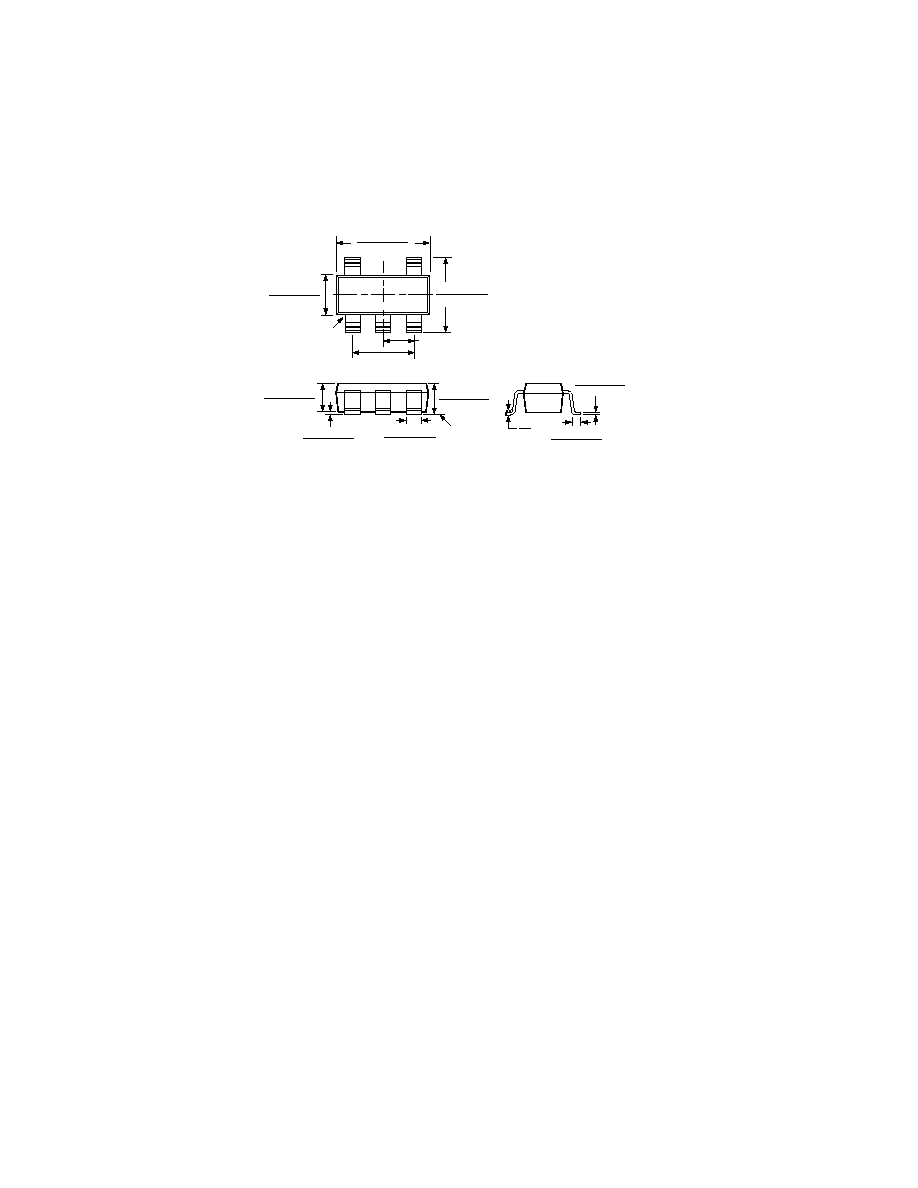
5-Lead SOT-23
(RT Suffix)
0.1181 (3.00)
0.1102 (2.80)
PIN 1
0.0669 (1.70)
0.0590 (1.50)
0.1181 (3.00)
0.1024 (2.60)
1
3
4
5
0.0748 (1.90)
BSC
0.0374 (0.95) BSC
2
0.0079 (0.20)
0.0031 (0.08)
0.0217 (0.55)
0.0138 (0.35)
10
0
0.0197 (0.50)
0.0138 (0.35)
0.0059 (0.15)
0.0019 (0.05)
0.0512 (1.30)
0.0354 (0.90)
SEATING
PLANE
0.0571 (1.45)
0.0374 (0.95)