 | ÐлекÑÑоннÑй компоненÑ: OP191G | СкаÑаÑÑ:  PDF PDF  ZIP ZIP |
OP191/291/491 Data Sheet
One Technology Way, P.O. Box 9106, Norwood, MA 02062-9106, U.S.A.
Tel: 781/329-4700
www.analog.com
Fax: 781/326-8703
© Analog Devices, Inc., 2002
REV. A
Information furnished by Analog Devices is believed to be accurate and
reliable. However, no responsibility is assumed by Analog Devices for its
use, nor for any infringements of patents or other rights of third parties that
may result from its use. No license is granted by implication or otherwise
under any patent or patent rights of Analog Devices.
a
OP191/OP291/OP491
GENERAL DESCRIPTION
The OP191, OP291, and OP491 are single, dual and quad
micropower, single-supply, 3 MHz bandwidth amplifiers fea-
turing rail-to-rail inputs and outputs. All are guaranteed to
operate from a 3 V single supply as well as
±5 V dual supplies.
Fabricated on Analog Devices' CBCMOS process, the OP191
family has a unique input stage that allows the input voltage to
safely extend 10 V beyond either supply without any phase inver-
sion or latch-up. The output voltage swings to within millivolts
of the supplies and continues to sink or source current all the
way to the supplies.
Applications for these amplifiers include portable telecom
equipment, power supply control and protection, and interface
for transducers with wide output ranges. Sensors requiring a
rail-to-rail input amplifier include Hall effect, piezo electric, and
resistive transducers.
The ability to swing rail-to-rail at both the input and output
enables designers to build multistage filters in single-supply
systems and maintain high signal-to-noise ratios.
The OP191/OP291/OP491 are specified over the extended
industrial (40
°C to +125°C) temperature range. The OP191
single and OP291 dual amplifiers are available in 8-lead plastic
SO surface mount packages
*
. The OP491 quad is available in
14-lead DIPs and narrow 14-lead SO packages. Consult factory
for OP491 TSSOP availability.
*
The OP291 dual is also available in 8-lead Plastic Dip.
Micropower Single-Supply
Rail-to-Rail Input/Output Op Amps
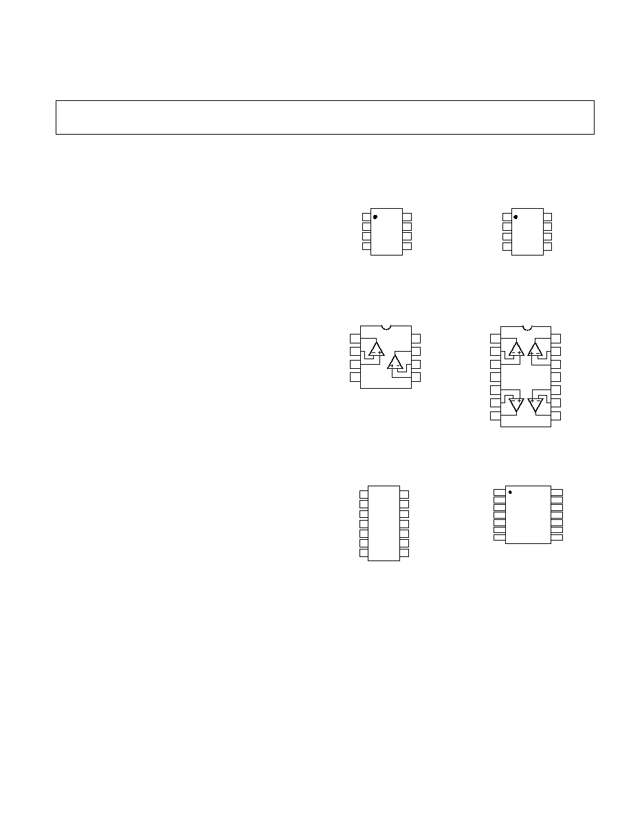
PIN CONFIGURATIONS
8-Lead Narrow-Body SO 8-Lead Narrow-Body SO
8-Lead Plastic DIP 14-Lead Plastic DIP
14-Lead SO 14-Lead TSSOP
FEATURES
Single-Supply Operation: 2.7 V to 12 V
Wide Input Voltage Range
Rail-to-Rail Output Swing
Low Supply Current: 300 A/Amp
Wide Bandwidth: 3 MHz
Slew Rate: 0.5 V/ s
Low Offset Voltage: 700 V
No Phase Reversal
APPLICATIONS
Industrial Process Control
Battery-Powered Instrumentation
Power Supply Control and Protection
Telecom
Remote Sensors
Low-Voltage Strain Gage Amplifiers
DAC Output Amplifier
1
2
3
4
8
7
6
5
OP191
1
2
3
4
8
7
6
5
OP291
1
2
3
4
8
7
6
5
OP291
OUTB
INB
+INB
+V
OUTA
INA
+INA
V
1
2
3
4
5
6
7
14
13
12
11
10
9
8
OP491
OUTD
IND
+IND
V
+INC
INC
OUTC
OUTA
INA
+INA
+V
+INB
INB
OUTB
1
2
3
4
5
6
7
14
13
12
11
10
9
8
OP491
OUTD
IND
+IND
V
+INC
INC
OUTC
OUTA
INA
+INA
+V
+INB
INB
OUTB
1
2
5
6
7
3
4
14
13
10
9
8
12
11
OP491

OP191/OP291/OP491SPECIFICATIONS
ELECTRICAL SPECIFICATIONS
Parameter
Symbol
Conditions
Min
Typ
Max
Unit
INPUT CHARACTERISTICS
Offset Voltage
OP191G
V
OS
80
500
µV
40
°C T
A
+125°C
1
mV
OP291/OP491G
V
OS
80
700
µV
40
°C T
A
+125°C
1.25
mV
Input Bias Current
I
B
30
65
nA
40
°C T
A
+125°C
95
nA
Input Offset Current
I
OS
0.1
11
nA
40
°C T
A
+125°C
22
nA
Input Voltage Range
0
3
V
Common-Mode Rejection Ratio
CMRR
V
CM
= 0 V to 2.9 V
70
90
dB
40
°C T
A
+125°C
65
87
dB
Large Signal Voltage Gain
A
VO
R
L
= 10 k
, V
O
= 0.3 V to 2.7 V
25
70
V/mV
40
°C T
A
+125°C
50
V/mV
Offset Voltage Drift
V
OS
/
T
1.1
µV/°C
Bias Current Drift
I
B
/
T
100
pA/
°C
Offset Current Drift
I
OS
/
T
20
pA/
°C
OUTPUT CHARACTERISTICS
Output Voltage High
V
OH
R
L
= 100 k
to GND
2.95
2.99
V
40
°C to +125°C
2.90
2.98
V
R
L
= 2 k
to GND
2.8
2.9
V
40
°C to +125°C
2.70
2.8
V
Output Voltage Low
V
OL
R
L
= 100 k
to V+
4.5
10
mV
40
°C to +125°C
35
mV
R
L
= 2 k
to V+
40
75
mV
40
°C to +125°C
130
mV
Short Circuit Limit
I
SC
Sink/Source
±8.75
±13.5
mA
40
°C to +125°C
±6.0
±10.5
mA
Open-Loop Impedance
Z
OUT
f = 1 MHz, A
V
= 1
200
POWER SUPPLY
Power Supply Rejection Ratio
PSRR
V
S
= 2.7 V to 12 V
80
110
dB
40
°C T
A
+125°C
75
110
dB
Supply Current/Amplifier
I
SY
V
O
= 0 V
200
350
µA
40
°C T
A
+125°C
330
480
µA
DYNAMIC PERFORMANCE
Slew Rate
+SR
R
L
= 10 k
0.4
V/
µs
Slew Rate
SR
R
L
= 10 k
0.4
V/
µs
Full-Power Bandwidth
BW
P
1% Distortion
1.2
kHz
Settling Time
t
S
To 0.01%
22
µs
Gain Bandwidth Product
GBP
3
MHz
Phase Margin
O
45
Degrees
Channel Separation
CS
f = 1 kHz, R
L
= 10 k
145
dB
NOISE PERFORMANCE
Voltage Noise
e
n
p-p
0.1 Hz to 10 Hz
2
µV p-p
Voltage Noise Density
e
n
f = 1 kHz
35
nV/
Hz
Current Noise Density
i
n
0.8
pA/
Hz
Specifications subject to change without notice.
(@ V
S
= +3.0 V, V
CM
= 0.1 V, V
O
= 1.4 V, T
A
= 25 C unless otherwise noted.)
REV. A
2

REV. A
3
ELECTRICAL SPECIFICATIONS
(@ V
S
= +5.0 V, V
CM
= 0.1 V, V
O
= 1.4 V, T
A
= 25 C unless otherwise noted.)
Parameter
Symbol
Conditions
Min
Typ
Max
Unit
INPUT CHARACTERISTICS
Offset Voltage
OP191
V
OS
80
500
µV
40
°C T
A
+125°C
1.0
mV
OP291/OP491
V
OS
80
700
µV
40
°C T
A
+125°C
1.25
mV
Input Bias Current
I
B
30
65
nA
40
°C T
A
+125°C
95
nA
Input Offset Current
I
OS
0.1
11
nA
40
°C T
A
+125°C
22
nA
Input Voltage Range
0
5
V
Common-Mode Rejection Ratio
CMRR
V
CM
= 0 V to 4.9 V
70
93
dB
40
°C T
A
+125°C
65
90
dB
Large Signal Voltage Gain
A
VO
R
L
= 10 k
, V
O
= 0.3 V to 4.7 V
25
70
V/mV
40
°C T
A
+125°C
50
V/mV
Offset Voltage Drift
V
OS
/
T
40
°C T
A
+125°C
1.1
µV/°C
Bias Current Drift
I
B
/
T
100
pA/
°C
Offset Current Drift
I
OS
/
T
20
pA/
°C
OUTPUT CHARACTERISTICS
Output Voltage High
V
OH
R
L
= 100 k
to GND
4.95
4.99
V
40
°C to +125°C
4.90
4.98
V
R
L
= 2 k
to GND
4.8
4.85
V
40
°C to +125°C
4.65
4.75
V
Output Voltage Low
V
OL
R
L
= 100 k
to V+
4.5
10
mV
40
°C to +125°C
35
mV
R
L
= 2 k
to V+
40
75
mV
40
°C to +125°C
155
mV
Short Circuit Limit
I
SC
Sink/Source
±8.75
±13.5
mA
40
°C to +125°C
±6.0
±10.5
mA
Open-Loop Impedance
Z
OUT
f = 1 MHz, A
V
= 1
200
POWER SUPPLY
Power Supply Rejection Ratio
PSRR
V
S
= 2.7 V to 12 V
80
110
dB
40
°C T
A
+125°C
75
110
dB
Supply Current/Amplifier
I
SY
V
O
= 0 V
220
400
µA
40
°C T
A
+125°C
350
500
µA
DYNAMIC PERFORMANCE
Slew Rate
+SR
R
L
= 10 k
0.4
V/
µs
Slew Rate
SR
R
L
= 10 k
0.4
V/
µs
Full-Power Bandwidth
BW
P
1% Distortion
1.2
kHz
Settling Time
t
S
To 0.01%
22
µs
Gain Bandwidth Product
GBP
3
MHz
Phase Margin
O
45
Degrees
Channel Separation
CS
f = 1 kHz, R
L
= 10 k
145
dB
NOISE PERFORMANCE
Voltage Noise
e
n
p-p
0.1 Hz to 10 Hz
2
µV p-p
Voltage Noise Density
e
n
f = 1 kHz
35
nV/
Hz
Current Noise Density
i
n
0.8
pA/
Hz
NOTE
+5 V specifications are guaranteed by +3 V and
±5 V testing.
Specifications subject to change without notice.
OP191/OP291/OP491
OP191/OP291/OP491
REV. A
4
ELECTRICAL SPECIFICATIONS
(@ V
O
= 5.0 V, 4.9 V
V
CM
+4.9 V, T
A
= 25 C unless otherwise noted.)
Parameter
Symbol
Conditions
Min
Typ
Max
Unit
INPUT CHARACTERISTICS
Offset Voltage
OP191
V
OS
80
500
µV
40
°C T
A
+125°C
1
mV
OP291/OP491
V
OS
80
700
µV
40
°C T
A
+125°C
1.25
mV
Input Bias Current
I
B
30
65
nA
40
°C T
A
+125°C
95
nA
Input Offset Current
I
OS
0.1
11
nA
40
°C T
A
+125°C
22
nA
Input Voltage Range
5
+5
V
Common-Mode Rejection
CMR
V
CM
=
±5 V
75
100
dB
40
°C T
A
+125°C
67
97
dB
Large Signal Voltage Gain
A
VO
R
L
= 10 k
, V
O
=
±4.7 V,
25
70
40
°C T
A
+125°C
50
V/mV
Offset Voltage Drift
V
OS
/
T
1.1
µV/°C
Bias Current Drift
I
B
/
T
100
pA/
°C
Offset Current Drift
I
OS
/
T
20
pA/
°C
OUTPUT CHARACTERISTICS
Output Voltage Swing
V
O
R
L
= 100 k
to GND
±4.93
±4.99
V
40
°C to +125°C
±4.90
±4.98
V
R
L
= 2 k
to GND
±4.80
±4.95
V
40
°C T
A
+125°C
±4.65
±4.75
V
Short Circuit Limit
I
SC
Sink/Source
±8.75
±16
mA
40
°C to +125°C
±6
±13
mA
Open-Loop Impedance
Z
OUT
f = 1 MHz, A
V
= 1
200
POWER SUPPLY
Power Supply Rejection Ratio
PSRR
V
S
=
±5 V
80
110
dB
40
°C T
A
+125°C
70
100
dB
Supply Current/Amplifier
I
SY
V
O
= 0 V
260
420
µA
40
T
A
+125°C
390
550
µA
DYNAMIC PERFORMANCE
Slew Rate
±SR
R
L
=10 k
0.5
V/
µs
Full-Power Bandwidth
BW
P
1% Distortion
1.2
kHz
Settling Time
t
S
To 0.01%
22
µs
Gain Bandwidth Product
GBP
3
MHz
Phase Margin
O
45
Degrees
Channel Separation
CS
f = 1 kHz
145
dB
NOISE PERFORMANCE
Voltage Noise
e
n
p-p
0.1 Hz to 10 Hz
2
µV p-p
Voltage Noise Density
e
n
f = 1 kHz
35
nV/
Hz
Current Noise Density
i
n
0.8
pA/
Hz
Specifications subject to change without notice.
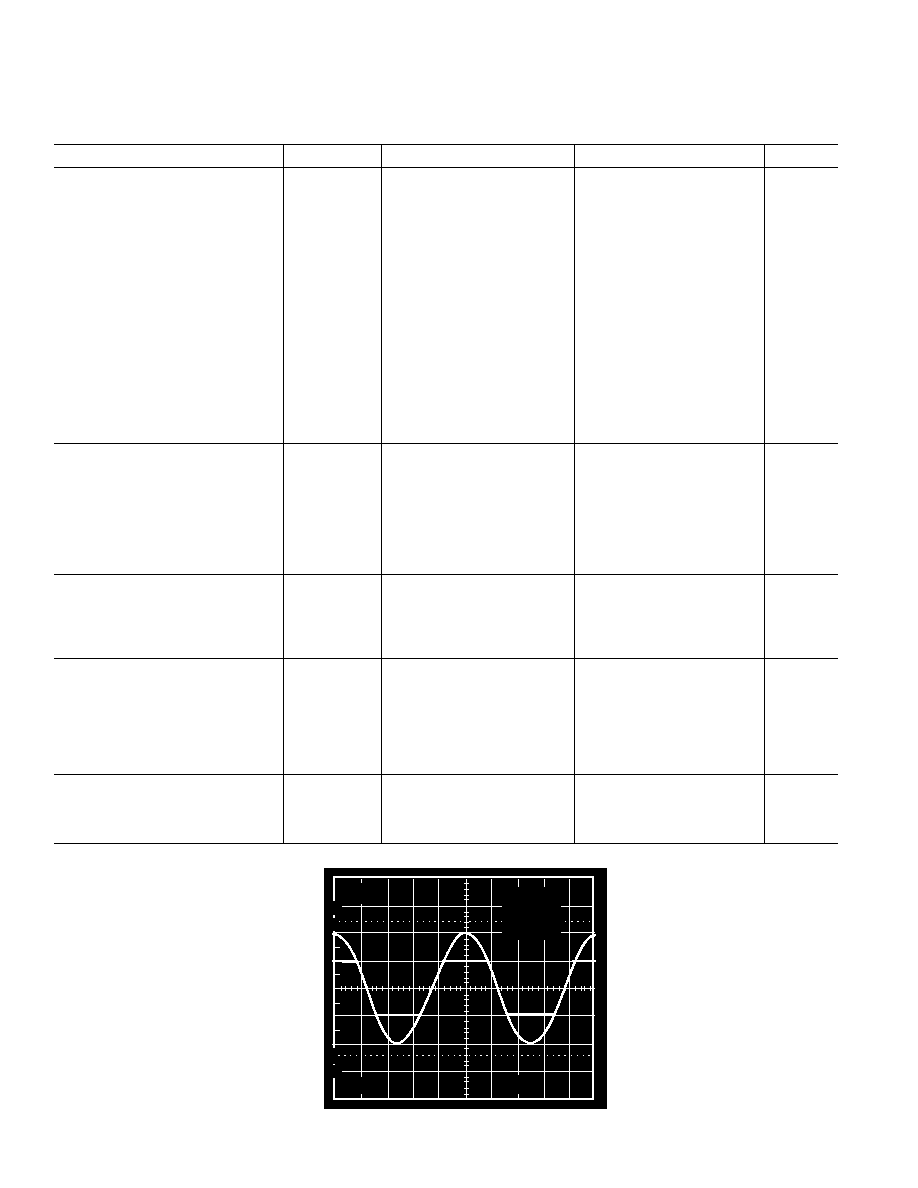
10
100
0%
90
5V
V
S
= 5V
R
L
= 2k
A
V
= +1
V
IN
= 20V p-p
200 s
5V
INPUT
OUTPUT
Figure 1. Input and Output with Inputs Overdriven by 5 V
OP191/OP291/OP491
REV. A
5
ABSOLUTE MAXIMUM RATINGS
1
Supply Voltage . . . . . . . . . . . . . . . . . . . . . . . . . . . . . . . . . 16 V
Input Voltage . . . . . . . . . . . . . . . . . . . . . . . . . GND to V
S
10 V
Differential Input Voltage . . . . . . . . . . . . . . . . . . . . . . . . . . 7 V
Output Short-Circuit Duration to GND . . . . . . . . . . Indefinite
Storage Temperature Range
P, S, RU Packages . . . . . . . . . . . . . . . . . . . 65
°C to +150°C
Operating Temperature Range
OP191/OP291/OP491G . . . . . . . . . . . . . . . 40
°C to +125°C
Junction Temperature Range
P, S, RU Packages . . . . . . . . . . . . . . . . . . . 65
°C to +150°C
Lead Temperature Range (Soldering 60 sec) . . . . . . . . +300
°C
Package Type
JA
2
JC
Units
8-Lead Plastic DIP (P)
103
43
°C/W
8-Lead SOIC (S)
158
43
°C/W
14-Lead Plastic DIP (P)
76
33
°C/W
14-Lead SOIC (S)
120
36
°C/W
14-Lead TSSOP (RU)
180
35
°C/W
NOTES
1
Absolute maximum ratings apply to both DICE and packaged parts, unless
otherwise noted.
2
JA
is specified for the worst case conditions; i.e.,
JA
is specified for device in socket
for P-DIP packages;
JA
is specified for device soldered in circuit board for TSSOP
and SOIC packages.
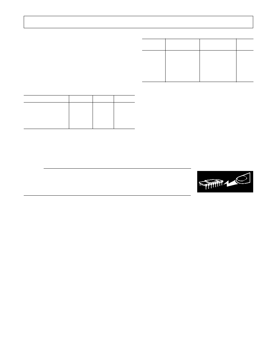
ORDERING GUIDE
Temperature
Package
Package
Model
Range
Description
Option
OP191GS
-40 C to +125 C
8-Lead SOIC
SO-8
OP291GP
*
-40 C to +125 C
8-Lead Plastic DIP
N-8
OP291GS
-40 C to +125 C
8-Lead SOIC
SO-8
OP491GP
-40 C to +125 C
14-Lead Plastic DIP N-14
OP491GS
-40 C to +125 C
14-Lead SOIC
SO-14
OP491GRU
-40 C to +125 C
14-Lead TSSOP
RU-14
*
Not for new design; obsolete April 2002.
CAUTION
ESD (electrostatic discharge) sensitive device. Electrostatic charges as high as 4000 V readily
accumulate on the human body and test equipment and can discharge without detection.
Although the OP191/OP291/OP491 feature proprietary ESD protection circuitry, permanent
damage may occur on devices subjected to high-energy electrostatic discharges. Therefore, proper
ESD precautions are recommended to avoid performance degradation or loss of functionality.
WARNING!
ESD SENSITIVE DEVICE
OP191/OP291/OP491Typical Performance Characteristics
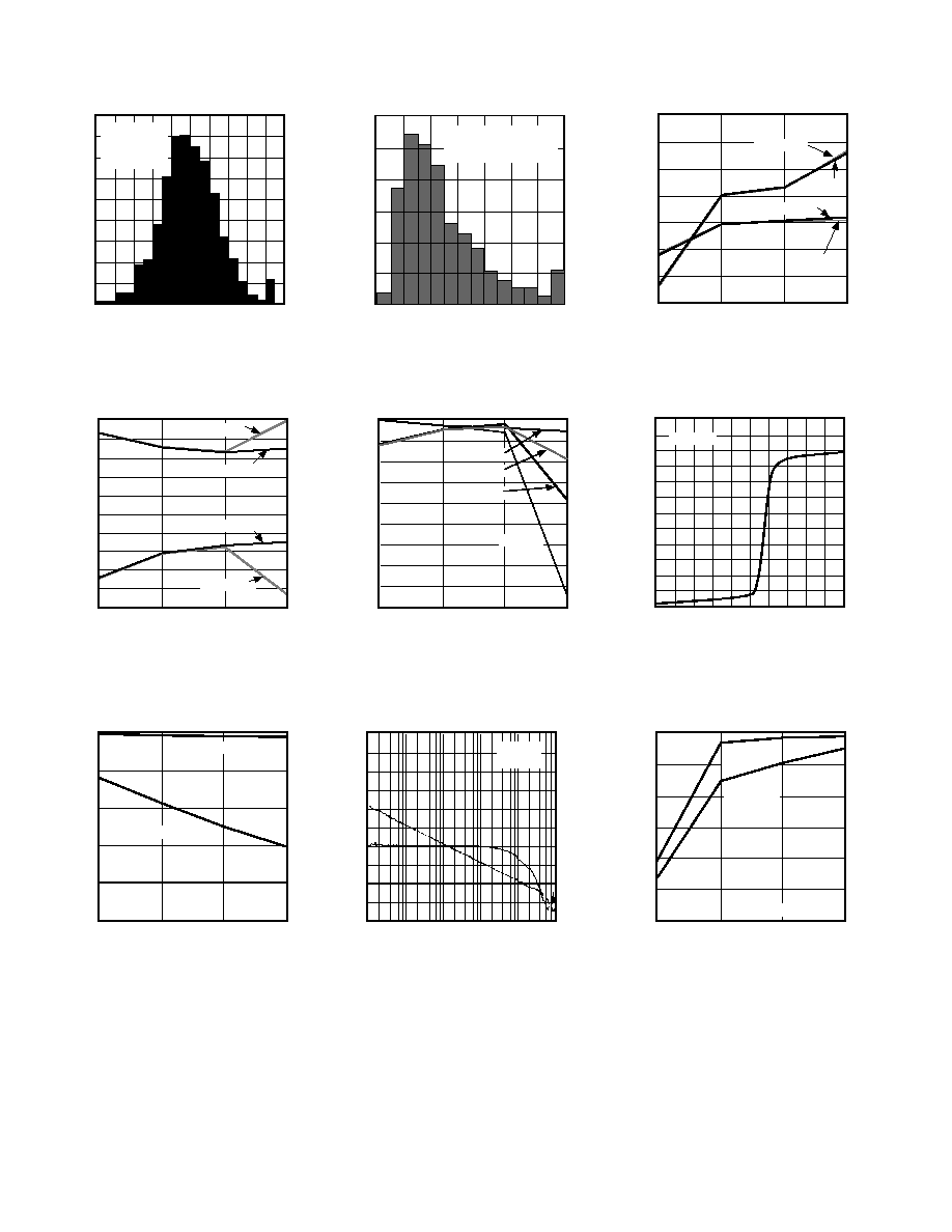
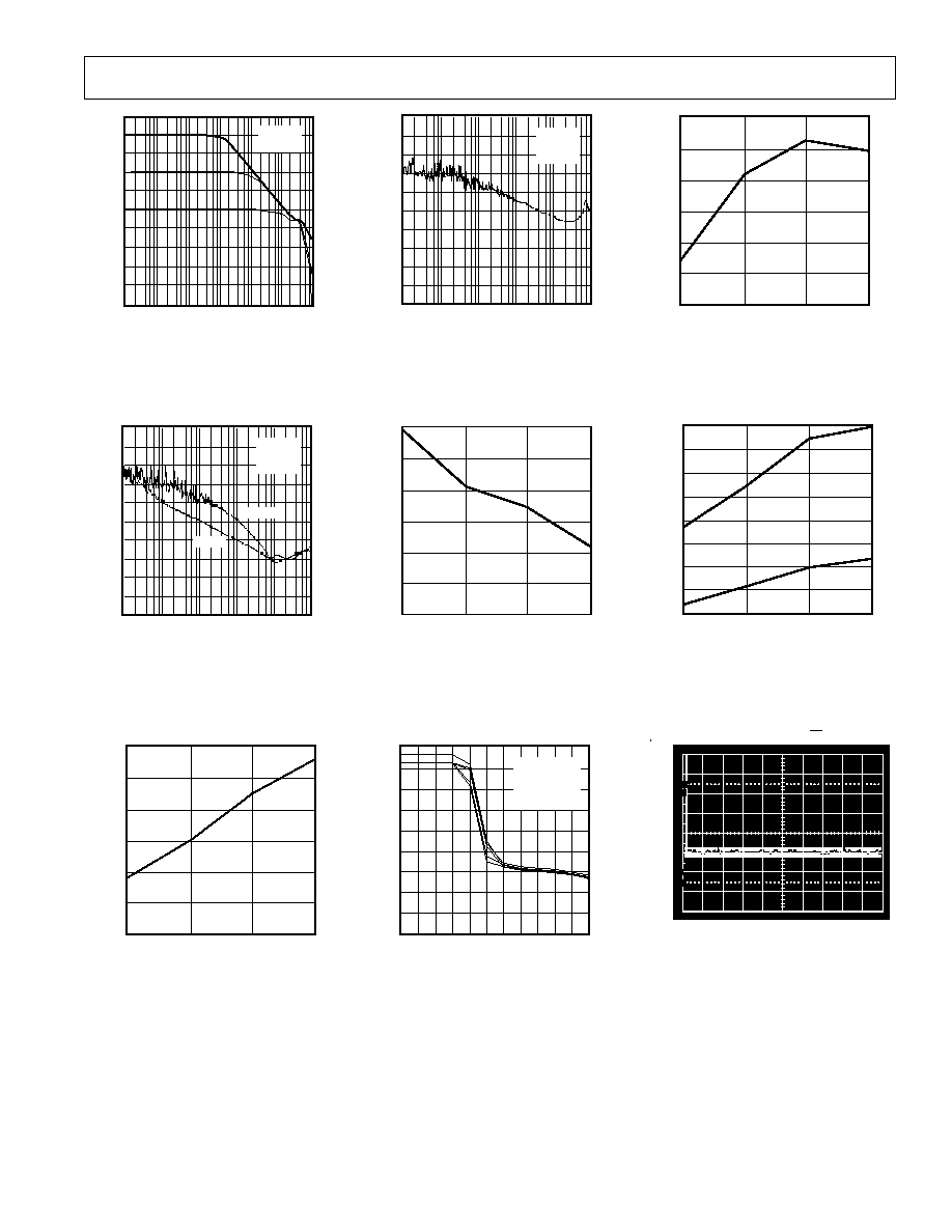
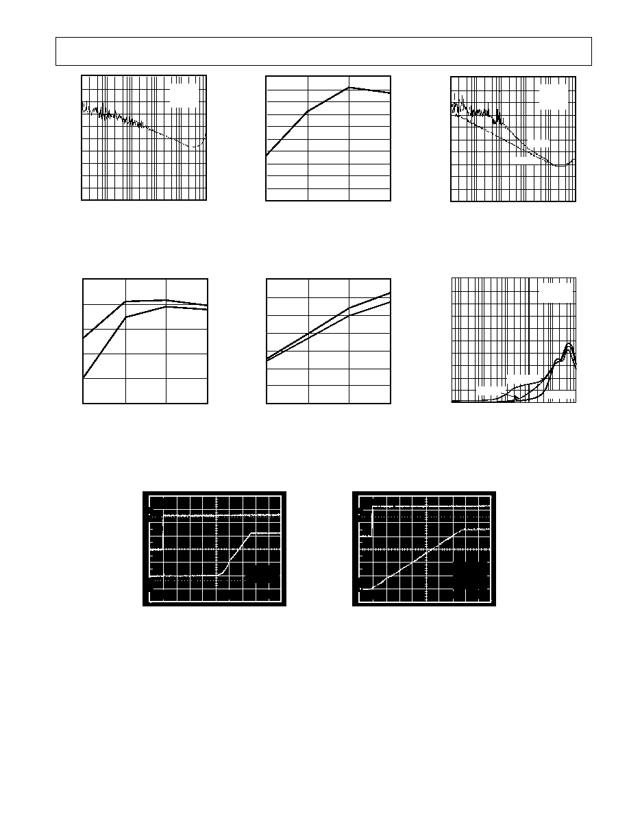
INPUT OFFSET VOLTAGE
mV
125
25
40
V
CM
= 0V
85
TEMPERATURE C
0
0.02
0.04
0.06
0.08
0.10
0.12
0.14
V
CM
= 2.9V
V
S
= +3V
V
CM
= 0.1V
V
CM
= 3V
TPC 3. Input Offset Voltage vs.
Temperature, V
S
= +3 V
36
36
3.0
18
30
0.30
24
0
0
12
6
6
12
18
30
24
2.7
2.4
2.1
1.8
1.5
1.2
0.90
0.60
INPUT COMMON-MODE VOLTAGE V
INPUT BIAS CURRENT
nA
V
S
= +3V
TPC 6. Input Bias Current vs. Com-
mon-Mode Voltage, V
S
= +3 V
1200
1000
800
600
400
200
0
125
25
40
85
TEMPERATURE C
OPEN-LOOP GAIN
V/mV
V
S
= 3V, V
O
= 0.3V/2.7V
R
L
= 100k ,
V
CM
= 2.9V
R
L
= 100k ,
V
CM
= 0.1V
TPC 9. Open-Loop Gain vs.
Temperature, V
S
= +3 V
INPUT OFFSET VOLTAGE V/ C
UNITS
120
0
7
60
20
1
40
0
100
80
6
4
3
2
5
V
S
= +3V
40 C < T
A
< +125 C
BASED ON 600 OP AMPS
TPC 2. OP291 Input Offset Volt-
age Drift Distribution, V
S
= +3 V
INPUT OFFSET CURRENT
nA
TEMPERATURE C
0
0.2
0.4
0.6
0.8
1.0
1.2
1.4
1.6
1.8
125
25
40
85
V
CM
= 0.1V
V
CM
= 2.9V
V
CM
= 3V
V
CM
= 0V
V
S
= +3V
TPC 5. Input Offset Current vs. Tem-
perature, V
S
= +3 V
160
100
60
40
1k
10k
100k
1M
10M
80
100
120
140
20
0
20
40
V
S
= +3V
T
A
= 25 C
OPEN-LOOP GAIN
dB
90
45
0
270
225
180
135
PHASE SHIFT
C
FREQUENCY Hz
TPC 8. Open-Loop Gain and Phase
vs. Frequency, V
S
= +3 V
180
0
0.22
40
20
0.18
60
80
100
120
140
160
0.14
0.06
0.02
0.10
INPUT OFFSET VOLTAGE mV
UNITS
V
S
= +3V
T
A
= 25 C
BASED ON
1200 OP AMPS
TPC 1. OP291 Input Offset Voltage
Distribution, V
S
= +3 V
INPUT BIAS CURRENT
nA
TEMPERATURE C
40
30
20
10
0
10
20
30
40
50
60
125
25
40
85
V
CM
= 0V
V
CM
= 0.1V
V
CM
= 2.9V
V
CM
= 3V
V
S
= +3V
TPC 4. Input Bias Current vs.
Temperature, V
S
= +3 V
OUTPUT SWING
V
V
S
= +3V
TEMPERATURE C
3.00
2.75
125
2.90
2.80
25
2.85
40
2.95
85
+V
O
@ R
L
= 100k
+V
O
@ R
L
= 2k
TPC 7. Output Voltage Swing vs.
Temperature, V
S
= +3 V
REV. A
6
OP191/OP291/OP491
REV. A
7
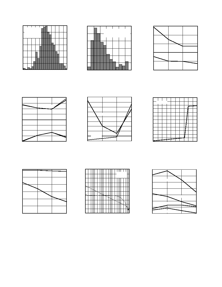
50
0
50
10
100
10M
1M
100k
10k
1k
10
20
30
40
40
30
20
10
CLOSED-LOOP GAIN
dB
V
S
= +3V
T
A
= 25 C
FREQUENCY Hz
TPC 10. Closed-Loop Gain vs.
Frequency, V
S
= +3 V
160
100
60
40
1k
10k
100k
1M
10M
80
100
120
140
20
0
20
40
PSRR
V
S
= +3V
T
A
= 25 C
PSRR
dB
PSRR
PSRR
FREQUENCY Hz
TPC 13. PSRR vs. Frequency,
V
S
= +3 V
V
S
= +3V
TEMPERATURE C
0.35
0.05
125
0.20
0.10
25
0.15
40
0.30
0.25
85
SUPPLY CURRENT/AMPLIFIER
mA
TPC 16. Supply Current vs.
Temperature, V
S
= +3 V, +5 V,
±5 V
160
100
60
40
1k
10k
100k
1M
10M
80
100
120
140
20
0
20
40
CMRR
V
S
= +3V
T
A
= 25 C
CMRR
dB
FREQUENCY Hz
TPC 11. CMRR vs. Frequency,
V
S
= +3 V
V
S
= +3V
TEMPERATURE C
113
107
125
110
108
25
109
40
112
111
85
PSRR
dB
TPC 14. PSRR vs. Temperature,
V
S
= +3 V
2.8
1.0
300
1.4
1.2
0.5
0.1
1.8
1.6
2.0
2.2
2.4
2.6
250
200
150
100
70
50
30
10
1.0
V
IN
= +2.8V p-p
V
S
= +3V
A
V
= +1
R
L
= 100k
FREQUENCY kHz
MAXIMUM OUTPUT SWING
V
TPC 17. Maximum Output Swing vs.
Frequency, V
S
= +3 V
V
S
= +3V
TEMPERATURE C
90
84
125
87
85
25
86
40
89
88
85
CMRR
dB
TPC 12. CMRR vs. Temperature,
V
S
= +3 V
SLEW RATE
V/
s
V
S
= +3V
TEMPERATURE C
1.6
0
125
0.4
0.2
25
40
0.8
0.6
1.0
1.2
1.4
85
SR
SR
TPC 15. Slew Rate vs. Tempera-
ture, V
S
= +3 V
90
10
0%
100
MKR: 36.2 nV/ Hz
MKR: 0 Hz
1000 Hz
BW: 2.5kHz
15.0 Hz
TPC 18. Voltage Noise Density,
V
S
= +3 V to
±5 V, A
VO
= 1000
V
OS
mV
V
S
= +5V
TEMPERATURE C
0.15
0.1
125
0.05
0.05
25
0
40
0.10
85
V
CM
= 0V
V
CM
= +5V
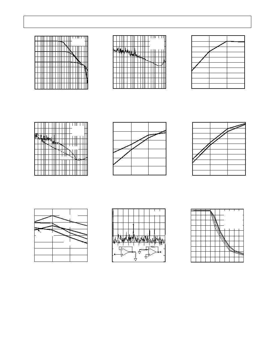
TPC 21. Input Offset Voltage vs.
Temperature, V
S
= +5 V
36
36
5
18
30
24
0
0
12
6
6
12
18
30
24
4
3
2
1
COMMON MODE INPUT VOLTAGE Volts
INPUT BIAS CURRENT
nA
V
S
= +5V
TPC 24. Input Bias Current vs.
Common-Mode Voltage, V
S
= +5 V
V
S
= +5V
TEMPERATURE C
140
0
125
60
20
25
40
40
120
80
100
85
OPEN-LOOP GAIN
V/mV
R
L
= 2k , V
CM
= 0V
R
L
= 100k , V
CM
= 5V
R
L
= 2k , V
CM
= 5V
R
L
= 100k , V
CM
= 0V
TPC 27. Open-Loop Gain vs.
Temperature, V
S
= +5 V
OP191/OP291/OP491
INPUT OFFSET VOLTAGE mV
UNITS
70
0
0.50
30
10
20
0.50
60
40
50
0.30
0.10
0.10
0.30
V
S
= +5V
T
A
= 25 C
BASED ON 600
OP AMPS
TPC 19. OP291 Input Offset Voltage
Distribution, V
S
= +5 V
I
B
nA
V
S
= +5V
TEMPERATURE C
40
40
125
20
30
25
40
0
10
10
20
30
85
+I
B
I
B
I
B
+I
B
V
CM
= 5V
V
CM
= 0V
TPC 22. Input Bias Current vs.
Temperature, V
S
= +5 V
V
S
= +5V
TEMPERATURE C
5.00
4.70
125
4.85
4.75
25
4.80
40
4.95
4.90
85
OUTPUT SWING
V
R
L
= 100k
R
L
= 2k
TPC 25. Output Voltage Swing vs.
Temperature, V
S
= +5 V
120
0
7.0
60
20
1.0
40
0
100
80
6.0
5.0
4.0
3.0
2.0
INPUT OFFSET VOLTAGE V/ C
UNITS
V
S
= +5V
40°C < T
A
< +125 C
BASED ON 600 OP AMPS
TPC 20. OP291 Input Offset
Voltage Drift Distribution, V
S
= +5 V
1.6
0.2
125
0.2
0
25
40
0.6
0.4
0.8
1.0
1.2
1.4
85
TEMPERATURE C
INPUT OFFSET CURRENT
nA
V
S
= +5V
V
CM
= 0V
V
CM
= 5V
TPC 23. Input Offset Current vs.
Temperature, V
S
= +5 V
160
100
60
40
1k
10k
100k
1M
10M
80
100
120
140
20
0
20
40
V
S
= +5V
T
A
= 25 C
OPEN-LOOP GAIN
dB
45
270
0
225
180
135
90
PHASE SHIFT
C
FREQUENCY Hz
TPC 26. Open-Loop Gain and Phase
vs. Frequency, V
S
= +5 V
REV. A
8
OP191/OP291/OP491
REV. A
9
50
0
50
10
100
10M
1M
100k
10k
1k
10
20
30
40
40
30
20
10
CLOSED-LOOP GAIN
dB
V
S
= +5V
T
A
= 25 C
FREQUENCY Hz
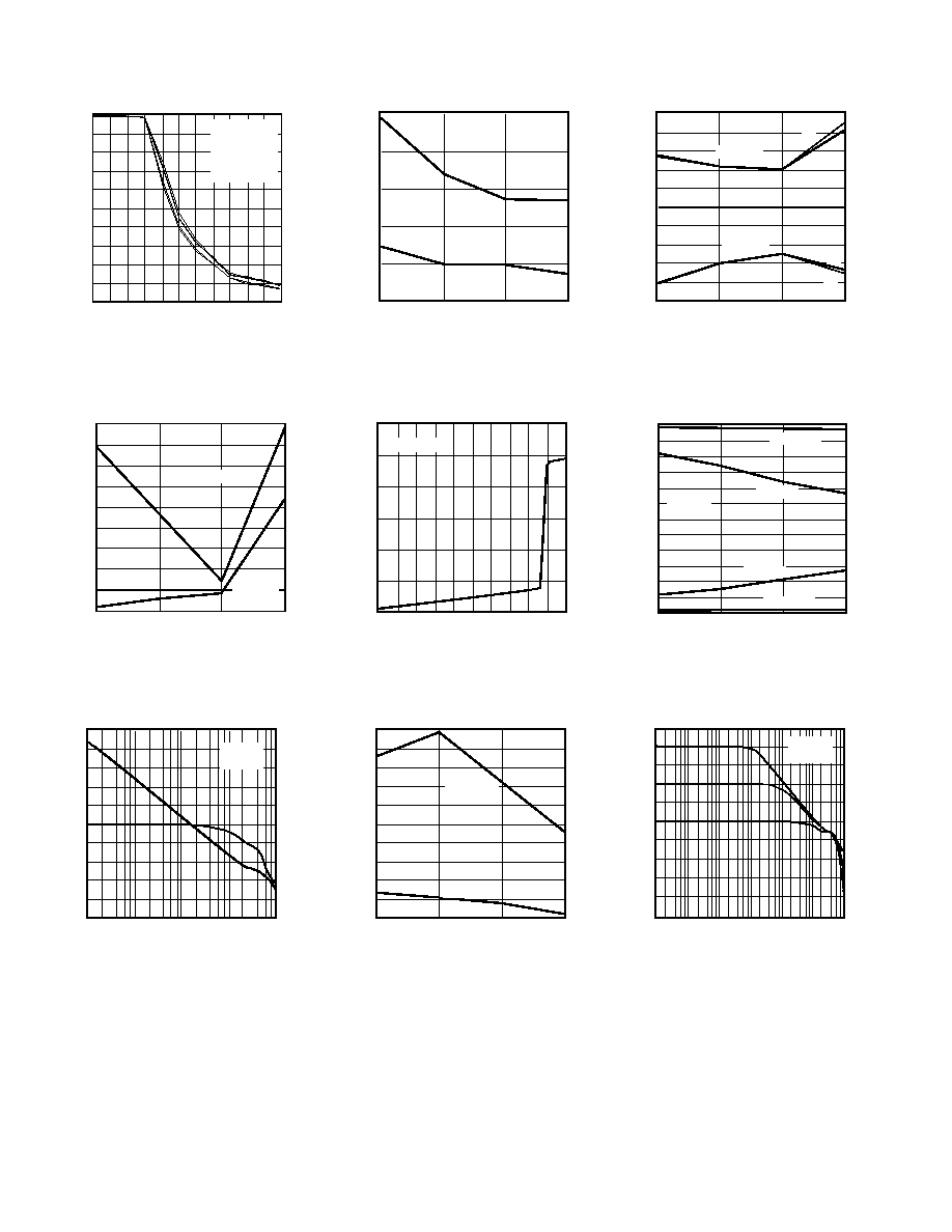
TPC 28. Closed-Loop Gain vs.
Frequency, V
S
= +5 V
160
100
60
40
1k
10k
100k
1M
10M
80
100
120
140
20
0
20
40
+PSRR
PSRR
PSRR
V
S
= +5V
T
A
= 25 C
PSRR
dB
FREQUENCY Hz
TPC 31. PSRR vs. Frequency,
V
S
= +5 V
SHORT CIRCUIT CURRENT
mA
TEMPERATURE C
20
4
125
8
6
25
40
12
10
14
16
18
85
+I
SC
,
V
S
= 5V
I
SC
, V
S
= 5V
+I
SC
,
V
S
= +3V
I
SC
,
V
S
= +3V
TPC 34. Short Circuit Current vs.
Temperature, V
S
= +3 V, +5 V,
±5 V
160
100
60
40
1k
10k
100k
1M
10M
80
100
120
140
20
0
20
40
CMRR
V
S
= +5V
T
A
= 25 C
CMRR
dB
FREQUENCY Hz
TPC 29. CMRR vs. Frequency,
V
S
= +5 V
V
S
= +5V
TEMPERATURE C
0.6
0
125
0.3
0.1
25
0.2
40
0.5
0.4
85
SR
V/
s
+SR
SR
TPC 32. OP291 Slew Rate vs.
Temperature, V
S
= +5 V
80
0
2500
20
10
0
40
30
50
60
70
2000
1500
1000
500
FREQUENCY Hz
VOLTAGE
V
V
S
= 5V
A
10k
V
IN
= 10V p-p @ 1kHz
B
10k
1k
V
O
TPC 35. Channel Separation,
V
S
=
±5 V
TEMPERATURE C
V
S
= +5V
96
86
89
87
25
88
40
92
90
91
93
94
95
85
CMRR
dB
125
TPC 30. CMRR vs. Temperature,
V
S
= +5 V
TEMPERATURE C
V
S
= +5V
0.50
0
125
0.15
0.05
25
0.10
40
0.30
0.20
0.25
0.35
0.40
0.45
85
SR
V/
s
+SR
SR
TPC 33. OP491 Slew Rate vs.
Temperature, V
S
= +5 V
FREQUENCY kHz
MAXIMUM OUTPUT SWING
V
5.0
0
300
1.5
0.5
0.5
1.0
0.1
3.0
2.0
2.5
3.5
4.0
4.5
250
100 150
50 70
200
30
10
1.0
V
IN
= +4.8V p-p
V
S
= +5V
A
V
= +1
R
L
= 100k
4 PARTS
TPC 36. Maximum Output Swing
vs. Frequency, V
S
= +5 V
OP191/OP291/OP491
REV. A
10
FREQUENCY kHz
MAXIMUM OUTPUT SWING
V
10
0
300
3
1
0.5
2
0.1
6
4
5
7
8
9
250
100 150
50 70
200
30
10
1.0
V
IN
= +9.8V p-p
V
S
= 5V
A
V
= +1
R
L
= 100k
4 PARTS
TPC 37. Maximum Output Swing vs.
Frequency, V
S
=
±5 V
1.6
0.2
125
0.2
0
25
40
0.6
0.4
0.8
1.0
1.2
1.4
85
TEMPERATURE C
INPUT OFFSET CURRENT
nA
V
S
= 5V
V
CM
= 5V
V
CM
= +5V
TPC 40. Input Offset Current vs.
Temperature, V
S
=
±5 V
70
20
30
1k
10k
10M
1M
100k
30
40
50
60
20
10
0
10
OPEN-LOOP GAIN
dB
90
45
0
270
225
180
135
PHASE SHIFT
C
V
S
= 5V
T
A
= 25 C
FREQUENCY Hz
TPC 43. Open-Loop Gain and Phase
vs. Frequency, V
S
=
±5 V
INPUT OFFSET VOLTAGE
mV
V
S
= 5V
TEMPERATURE C
0.15
0.1
125
0.05
0.05
25
0
40
0.10
85
V
CM
= +5V
V
CM
= 5V
TPC 38. Input Offset Voltage vs.
Temperature, V
S
=
±5 V
36
36
5
24
0
0
12
12
24
4
3
2
1
COMMON-MODE INPUT VOLTAGE V
INPUT BIAS CURRENT
nA
V
S
= 5V
1
2
3
4
5
TPC 41. Input Bias Current vs. Com-
mon-Mode Voltage, V
S
=
±5 V
TEMPERATURE C
V
S
= 5V
200
0
125
65
25
25
40
40
120
80
100
140
160
180
85
OPEN-LOOP GAIN
V/mV
R
L
= 100k
R
L
= 2k
TPC 44. Open-Loop Gain vs.
Temperature, V
S
=
±5 V
TEMPERATURE C
V
S
= 5V
50
50
125
20
40
25
30
40
10
10
0
20
30
40
85
I
B
nA
+I
B
+I
B
I
B
I
B
V
CM
= +5V
V
CM
= 5V
TPC 39. Input Bias Current vs.
Temperature, V
S
=
±5 V
5.00
5.00
125
4.85
4.95
25
4.90
40
0
4.80
4.75
4.75
4.80
4.85
4.95
4.90
85
OUTPUT VOLTAGE SWING
V
TEMPERATURE C
V
S
= 5V
R
L
= 100k
R
L
= 2k
R
L
= 100k
R
L
= 2k
TPC 42. Output Voltage Swing vs.
Temperature, V
S
=
±5 V
50
0
50
10
100
10M
1M
100k
10k
1k
10
20
30
40
40
30
20
10
CLOSED-LOOP GAIN
dB
V
S
= 5V
T
A
= 25 C
FREQUENCY Hz
TPC 45. Closed-Loop Gain vs.
Frequency, V
S
=
±5 V
OP191/OP291/OP491
REV. A
11
160
100
60
40
1k
10k
100k
1M
10M
80
100
120
140
20
0
20
40
CMRR
V
S
=
5V
T
A
= 25 C
CMRR
dB
FREQUENCY Hz
TPC 46. CMRR vs. Frequency,
V
S
=
±5 V
PSRR
dB
V
S
= 5V
TEMPERATURE C
115
90
125
105
95
25
100
40
110
85
OP491
OP291
TPC 49. OP291/OP491 PSRR vs.
Temperature, V
S
=
±5 V
TEMPERATURE C
V
S
= 5V
102
92
125
95
93
25
94
40
98
96
97
99
100
101
85
CMRR
dB
TPC 47. CMRR vs. Temperature,
V
S
=
±5 V
V
S
= 5V
TEMPERATURE C
0.7
0
125
0.3
0.1
25
0.2
40
0.6
0.4
0.5
85
SR
V/
s
+SR
SR
TPC 50. Slew Rate vs. Temperature,
V
S
=
±5 V
160
100
60
40
1k
10k
100k
1M
10M
80
100
120
140
20
0
20
40
+PSRR
PSRR
PSRR
V
S
=
5V
T
A
= 25 C
PSRR
dB
FREQUENCY Hz
TPC 48. PSRR vs. Frequency,
V
S
=
±5 V
1k
500
0
100
1k
10M
1M
100k
10k
600
700
800
900
100
200
300
400
Z
OUT
V
S
= +3V
T
A
= 25 C
A
VCL
= 100
A
VCL
= 10
A
VCL
= +1
FREQUENCY Hz
TPC 51. Output Impedance vs.
Frequency
10
100
0%
90
100mV
1.00V
2.00V
V
S
= 5V
R
L
= 200k
A
V
= +1V/V
INPUT
OUTPUT
2.00 s
TPC 53. Large Signal Transient
Response, V
S
=
±5 V
10
100
0%
90
100mV
500mV
1.00V
V
S
= +3V
R
L
= 200k
2.00 s
INPUT
OUTPUT
TPC 52. Large Signal Transient
Response, V
S
= +3 V
OP191/OP291/OP491
REV. A
12
exceeds approximately 0.6 V. In this condition, current will flow
between the input pins, limited only by the two 5 k
resistors.
Being aware of this characteristic is important in circuits where
the amplifier may be operated open-loop, such as a comparator.
Evaluate each circuit carefully to make sure that the increase in
current does not affect the performance.
The output stage of the OP191 family uses a PNP and an NPN
transistor as do most output stages; however, the output tran-
sistors, Q32 and Q33, are actually connected with their collec-
tors to the output pin to achieve the rail-to-rail output swing. As
the output voltage approaches either the positive or negative
rail, these transistors begin to saturate. Thus, the final limit on
output voltage is the saturation voltage of these transistors,
which is about 50 mV. The output stage does have inherent gain
arising from the collectors and any external load impedance.
Because of this, the open-loop gain of the amplifier is dependent
on the load resistance.
Input Overvoltage Protection
As with any semiconductor device, whenever the condition
exists for the input to exceed either supply voltage, attention
needs to be paid to the input overvoltage characteristic. When
an overvoltage occurs, the amplifier could be damaged depend-
ing on the voltage level and the magnitude of the fault current.
Figure 3 shows the characteristic for the OP191 family. This
graph was generated with the power supplies at ground and a
curve tracer connected to the input. As can be seen, when the
input voltage exceeds either supply by more than 0.6 V, internal
pn-junctions energize, allowing current to flow from the input to
the supplies. As described above, the OP291/OP491 does have
5 k
resistors in series with each input, which helps limit the
current. Calculating the slope of the current versus voltage in
the graph confirms the 5 k
resistor.
FUNCTIONAL DESCRIPTION
The OP191/OP291/OP491 are single-supply, micropower
amplifiers featuring rail-to-rail inputs and outputs. In order to
achieve wide input and output ranges, these amplifiers employ
unique input and output stages. As the simplified schematic
shows (Figure 2), the input stage is actually comprised of two
differential pairs, a PNP pair and an NPN pair. These two stages
do not actually work in parallel. Instead, only one or the other
stage is on for any given input signal level. The PNP stage (tran-
sistors Q1 and Q2) is required to ensure that the amplifier remains
in the linear region when the input voltage approaches and
reaches the negative rail. On the other hand, the NPN stage
(transistors Q5 and Q6) is needed for input voltages up to and
including the positive rail.
For the majority of the input common-mode range, the PNP
stage is active, as is evidenced by examining the graph of Input
Bias Current vs. Common-Mode Voltage. Notice that the bias
current switches direction at approximately 1.2 V to 1.3 V below
the positive rail. At voltages below this, the bias current flows
out of the OP291, indicating a PNP input stage. Above this
voltage, however, the bias current enters the device, revealing the
NPN stage. The actual mechanism within the amplifier for
switching between the input stages is comprised of the transistors
Q3, Q4, and Q7. As the input common-mode voltage increases,
the emitters of Q1 and Q2 follow that voltage plus a diode drop.
Eventually the emitters of Q1 and Q2 are high enough to turn
Q3 on. This diverts the 8
µA of tail current away from the PNP
input stage, turning it off. Instead, the current is mirrored through
Q4 and Q7 to activate the NPN input stage.
Notice that the input stage includes 5 k
series resistors and
differential diodes, a common practice in bipolar amplifiers to
protect the input transistors from large differential voltages.
These diodes will turn on whenever the differential voltage
Q1 Q2
8 A
5k
Q3
5k
IN
Q5 Q6
Q11
Q10
Q8
Q7
Q4
Q13
Q15
Q14
Q12
Q9
Q16
Q17
Q18
Q19
Q20
Q21
Q24
Q23
Q22
Q27
Q26
Q30
Q31
Q28
Q25
Q29
Q32
V
OUT
Q33
10pF
+IN
Figure 2. Simplified Schematic
OP191/OP291/OP491
REV. A
13
2mA
1mA
1mA
2mA
5V
10V
10V
5V
I
IN
V
IN
Figure 3. Input Overvoltage Characteristics
This input current is not inherently damaging to the device as
long as it is limited to 5 mA or less. In the case shown, for an
input of 10 V over the supply, the current is limited to 1.8 mA.
If the voltage is large enough to cause more than 5 mA of current
to flow, then an external series resistor should be added. The size
of this resistor is calculated by dividing the maximum overvoltage
by 5mA and subtracting the internal 5 k
resister. For example,
if the input voltage could reach 100 V, the external resistor
should be (100 V/5 mA) 5 k = 15 k
. This resistance should
be placed in series with either or both inputs if they are subjected
to the overvoltages. For more information on general overvoltage
characteristics of amplifiers refer to the 1993 System Applications
Guide, available from the Analog Devices Literature Center.
Output Voltage Phase Reversal
Some operational amplifiers designed for single-supply opera-
tion exhibit an output voltage phase reversal when their inputs
are driven beyond their useful common-mode range. Typically
for single-supply bipolar op amps, the negative supply deter-
mines the lower limit of their common-mode range. With these
devices, external clamping diodes, with the anode connected to
1/2
OP291
+5V
V
OUT
V
IN
20V p-p
10
90
100
0%
TIME 200 s/DIV
V
IN
2.5V/DIV
10
90
100
0%
20mV
20mV
5 s
V
OUT
2V/DIV
TIME 200 s/DIV
5 s
3
1
2
5V
4
8
Figure 4. Output Voltage Phase Reversal Behavior
ground and the cathode to the inputs, prevent input signal excur-
sions from exceeding the device's negative supply (i.e., GND),
preventing a condition which could cause the output voltage to
change phase. JFET-input amplifiers may also exhibit phase
reversal, and, if so, a series input resistor is usually required to
prevent it.
The OP191 family is free from reasonable input voltage range
restrictions due to its novel input structure. In fact, the input
signal can exceed the supply voltage by a significant amount
without causing damage to the device. As illustrated in Figure 4,
the OP191 family can safely handle a 20 V p-p input signal on
± 5 V supplies without exhibiting any sign of output voltage
phase reversal or other anomalous behavior. Thus no external
clamping diodes are required.
Overdrive Recovery
The overdrive recovery time of an operational amplifier is the
time required for the output voltage to recover to its linear region
from a saturated condition. This recovery time is important in
applications where the amplifier must recover quickly after a
large transient event, such as a comparator. The circuit shown
in Figure 5 was used to evaluate the OP191 family's overload
recovery time. The OP191 family takes approximately 8
µs to
recover from positive saturation and approximately 6.5
µs to
recover from negative saturation.
1/2
OP291
V
OUT
R1
9k
R2
10k
R3
10k
V
S
= 5V
V
IN
10V STEP
3
2
1
Figure 5. Overdrive Recovery Time Test Circuit
OP191/OP291/OP491
REV. A
14
Single-Supply RTD Amplifier
The circuit in Figure 7 uses three op amps of the OP491 to
develop a bridge configuration for an RTD amplifier that oper-
ates from a single +5 V supply. The circuit takes advantage of
the OP491's wide output swing range to generate a high bridge
excitation voltage of 3.9 V. In fact, because of the rail-to-rail
output swing, this circuit will work with supplies as low as 4.0 V.
Amplifier A1 servos the bridge to create a constant excitation
current in conjunction with the AD589, a 1.235 V precision
reference. The op amp maintains the reference voltage across
the parallel combination of the 6.19 k
and 2.55 M resistor,
which generates a 200
µA current source. This current splits
evenly and flows through both halves of the bridge. Thus, 100
µA
flows through the RTD to generate an output voltage based on
its resistance. A 3-wire RTD is used to balance the line resis-
tance in both 100
legs of the bridge to improve accuracy.
1/4
OP491
V
OUT
365
365
1/4
OP491
100k
0.01pF
A3
+5V
GAIN = 274
100k
1/4
OP491
37.4k
+5V
AD589
2.55M
6.19k
200
10-TURNS
26.7k
26.7k
A2
A1
100
100
RTD
ALL RESISTORS 1% OR BETTER
Figure 7. Single-Supply RTD Amplifier
Amplifiers A2 and A3 are configured in the two op amp IA
discussed above. Their resistors are chosen to produce a gain of
274, such that each 1
°C increase in temperature results in a
10 mV change in the output voltage, for ease of measurement.
A 0.01
µF capacitor is included in parallel with the 100 k
resistor on amplifier A3 to filter out any unwanted noise from
this high gain circuit. This particular RC combination creates a
pole at 1.6 kHz.
APPLICATIONS
Single +3 V Supply, Instrumentation Amplifier
The OP291's low supply current and low voltage operation make
it ideal for battery-powered applications such as the instrumen-
tation amplifier shown in Figure 6. The circuit utilizes the classic
two op amp instrumentation amplifier topology, with four resistors
to set the gain. The equation is simply that of a noninverting
amplifier as shown in the figure. The two resistors labeled R1
should be closely matched to each other as well as both resistors
labeled R2 to ensure good common-mode rejection performance.
Resistor networks ensure the closest matching as well as matched
drifts for good temperature stability. Capacitor C1 is included
to limit the bandwidth and, therefore, the noise in sensitive
applications. The value of this capacitor should be adjusted
depending on the desired closed-loop bandwidth of the instru-
mentation amplifier. The RC combination creates a pole at a
frequency equal to 1/(2
× R1C1). If AC-CMRR is critical,
than a matched capacitor to C1 should be included across the
second resistor labeled R1.
1/2
OP291
V
OUT
R1
R2
R2
1/2
OP291
R1
C1
100pF
V
IN
+3V
V
OUT
= (1 + ) V
IN
R1
R2
3
2
1
5
6
7
8
4
Figure 6. Single +3 V Supply Instrumentation Amplifier
Because the OP291 accepts rail-to-rail inputs, the input common-
mode range includes both ground and the positive supply of 3
V. Furthermore, the rail-to-rail output range ensures the widest
signal range possible and maximizes the dynamic range of the
system. Also, with its low supply current of 300
µA/device, this
circuit consumes a quiescent current of only 600
µA, yet still
exhibits a gain bandwidth of 3 MHz.
A question may arise about other instrumentation amplifier
topologies for single-supply applications. For example, a variation
on this topology adds a fifth resistor between the two inverting
inputs of the op amps for gain setting. While that topology works
well in dual-supply applications, it is inherently not appropriate
for single-supply circuits. The same could be said for the tradi-
tional three op amp instrumentation amplifier. In both cases, the
circuits simply will not work in single-supply situations unless a
false ground between the supplies is created.
OP191/OP291/OP491
REV. A
15
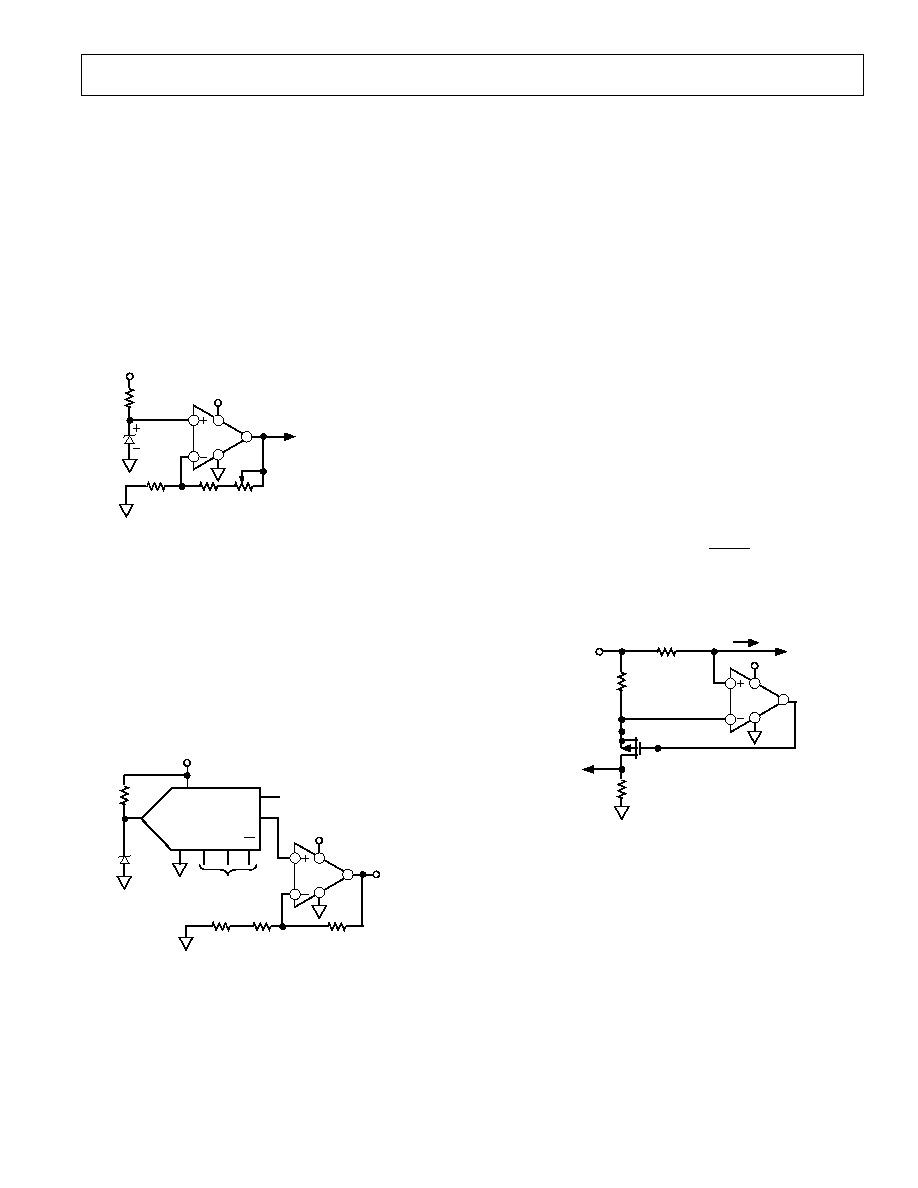
A +2.5 V Reference from a +3 V Supply
In many single-supply applications, the need for a 2.5 V reference
often arises. Many commercially available monolithic 2.5 V
references require at least a minimum operating supply voltage
of 4 V. The problem is exacerbated when the minimum operating
system supply voltage is +3 V. The circuit illustrated in Figure 8
is an example of a +2.5 V that operates from a single +3 V supply.
The circuit takes advantage of the OP291's rail-to-rail input and
output voltage ranges to amplify an AD589's 1.235 V output to
+2.5 V. The OP291's low TCV
OS
of 1
µV/°C helps maintain an
output voltage temperature coefficient of less than 200 ppm/
°C.
The circuit's overall temperature coefficient is dominated by R2
and R3's temperature coefficient. Lower tempco resistors are
recommended. The entire circuit draws less than 420
µA from a
+3 V supply at 25
°C.
RESISTORS = 1%, 100ppm/ C
POTENTIOMETER = 10 TURN, 100ppm/ C
R3
100k
1/2
OP291
R2
100k
+3V
R1
5k
+2.5V
REF
R1
17.4k
AD589
+3V
3
2
1
8
4
Figure 8. A +2.5 V Reference that Operates on a Single
+3 V Supply
+5 V Only, 12-Bit DAC Swings Rail-to-Rail
The OP191 family is ideal for use with a CMOS DAC to generate
a digitally controlled voltage with a wide output range. Figure 9
shows the DAC8043 used in conjunction with the AD589 to
generate a voltage output from 0 V to 1.23 V. The DAC is actu-
ally operated in "voltage switching" mode where the reference is
connected to the current output, I
OUT
, and the output voltage is
taken from the V
REF
pin. This topology is inherently noninverting
as opposed to the classic current output mode, which is inverting
and, therefore, unsuitable for single supply.
+5V
R1
17.8k
AD589
R2
R3
R4
232
1%
32.4k
1%
100k
1%
V
OUT
= (5V)
D
4096
GND CLK SR1
4
7
6
5
DIGITAL
CONTROL
LD
V
REF
R
FB
V
DD
I
OUT
2
3
8
1.23V
+5V
DAC8043
1/2
OP291
3
2
1
8
4
1
Figure 9. +5 V Only, 12-Bit DAC Swings Rail-to-Rail
The OP291 serves two functions. First, it is required to buffer
the high output impedance of the DAC's V
REF
pin, which is on
the order of 10 k
. The op amp provides a low impedance output
to drive any following circuitry. Secondly, the op amp amplifies
the output signal to provide a rail-to-rail output swing. In this
particular case, the gain is set to 4.1 to generate a 5.0 V output
when the DAC is at full scale. If other output voltage ranges are
needed, such as 0 to 4.095, the gain can easily be adjusted by
altering the value of the resistors.
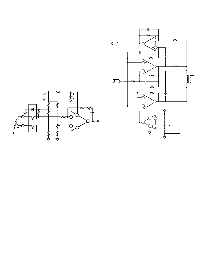
A High-Side Current Monitor
In the design of power supply control circuits, a great deal of
design effort is focused on ensuring a pass transistor's long-term
reliability over a wide range of load current conditions. As a
result, monitoring and limiting device power dissipation is of prime
importance in these designs. The circuit illustrated in Figure 10
is an example of a +5 V, single-supply high-side current monitor
that can be incorporated into the design of a voltage regulator
with fold-back current limiting or a high current power supply
with crowbar protection. This design uses an OP291's rail-to-rail
input voltage range to sense the voltage drop across a 0.1
current shunt. A p-channel MOSFET used as the feedback
element in the circuit converts the op amp's differential input
voltage into a current. This current is then applied to R2 to
generate a voltage that is a linear representation of the load
current. The transfer equation for the current monitor is given by:
Monitor Output = R2
I
L
×
×
R
R
SENSE
1
For the element values shown, the Monitor Output's transfer
characteristic is 2.5 V/A.
+5V
R
SENSE
0.1
+5V
+5V
I
L
S
G
M1
3N163
D
R2
2.49k
MONITOR
OUTPUT
R1
100
1/2
OP291
3
2
1
8
4
Figure 10. A High-Side Load Current Monitor
OP191/OP291/OP491
REV. A
16
A +3 V, Cold Junction Compensated Thermocouple Amplifier
The OP291's low supply operation makes it ideal for +3 V battery-
powered applications such as the thermocouple amplifier shown
in Figure 11. The K-type thermocouple terminates in an iso-
thermal block where the junctions' ambient temperature is
continuously monitored using a simple 1N914 diode. The diode
corrects the thermal EMF generated in the junctions by feeding
a small voltage, scaled by the 1.5 M
and 475 resistors, to
the op amp.
To calibrate this circuit, immerse the thermocouple measuring
junction in a 0
°C ice bath, and adjust the 500 pot to zero volts
out. Next, immerse the thermocouple in a 250
°C temperature
bath or oven and adjust the Scale Adjust pot for an output
voltage of 2.50 V. Within this temperature range, the K-type
thermocouple is accurate to within
±3°C without linearization.
8
1
4
3
2
OP291
500
10-TURN
ZERO
ADJUST
24.3k
1%
7.15k
1%
24.9k
1%
2.1k
1%
475
1%
1.5M
1%
1N914
AL
CR
ISOTHERMAL
BLOCK
ALUMEL
CHROMEL
COLD
JUNCTIONS
K-TYPE
THERMOCOUPLE
40.7 V/ C
10k
3.0V
AD589
1.33M
20k
SCALE
ADJUST
V
OUT
0V = 0 C
3V = 300 C
1.235V
11.2mV
4.99k
1%
Figure 11. A 3 V, Cold Junction Compensated Thermo-
couple Amplifier
Single-Supply, Direct Access Arrangement for Modems
An important building block in modems is the telephone line
interface. In the circuit shown in Figure 12, a direct access
arrangement is utilized for transmitting and receiving data from
the telephone line. Amplifier A1 is the receiving amplifier, and
amplifiers A2 and A3 are the transmitters. The forth amplifier,
A4, generates a pseudo ground half-way between the supply
voltage and ground. This pseudo ground is needed for the ac
coupled bipolar input signals.
The transmit signal, TXA, is inverted by A2 and then reinverted
by A3 to provide a differential drive to the transformer, where
each amplifier supplies half the drive signal. This is needed
because of the smaller swings associated with a single supply as
opposed to a dual supply. Amplifier A1 provides some gain for
the received signal, and it also removes the transmit signal present
at the transformer from the receive signal. To do this, the drive
signal from A2 is also fed to the noninverting input of A1 to
cancel the transmit signal from the transformer.
RXA
1/4
OP491
37.4k
A1
3.3k
0.0047 F
A2
20k , 1%
475 , 1%
0.033 F
37.4k , 1%
390pF
750pF
0.1 F
0.1 F
A3
T1
1:1
5.1V TO 6.2V
ZENER 5
A4
100k
100k
+3V OR +5V
10 F
0.1 F
20k , 1%
20k , 1%
20k 1%
TXA
20k 1%
13
12
14
8
10
9
1/4
OP491
7
6
5
1/4
OP491
3
1
2
1/4
OP491
4
11
Figure 12. Single-Supply Direct Access Arrangement for
Modems
The OP491's bandwidth of 3 MHz and rail-to-rail output swings
ensures that it can provide the largest possible drive to the trans-
former at the frequency of transmission.
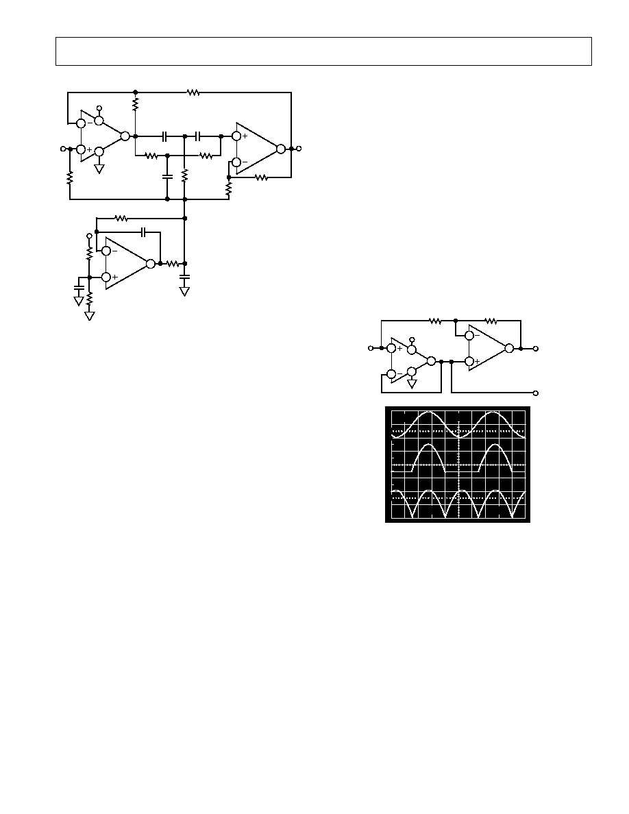
A +3 V, 50 Hz/60 Hz Active Notch Filter with False Ground
To process ac signals in a single-supply system, it is often best
to use a false-ground biasing scheme. A circuit that uses this
approach is illustrated in Figure 13. In this circuit, a false-ground
circuit biases an active notch filter used to reject 50 Hz/60 Hz
power line interference in portable patient monitoring equipment.
Notch filters are quite commonly used to reject power line
frequency interference which often obscures low frequency
physiological signals, such as heart rates, blood pressure readings,
EEGs, and EKGs. This notch filter effectively squelches 60 Hz
pickup at a filter Q of 0.75. Substituting 3.16 k
resistors for
the 2.67 k
resistors in the twin-T section (R1 through R5)
configures the active filter to reject 50 Hz interference.
OP191/OP291/OP491
REV. A
17
Single-Supply Half-Wave and Full-Wave Rectifiers
An OP191 family configured as a voltage follower operating on
a single supply can be used as a simple half-wave rectifier in
low-frequency (<2 kHz) applications. A full-wave rectifier can
be configured with a pair of OP291s as illustrated in Figure 14.
The circuit works in the following way: When the input signal is
above 0 V, the output of amplifier A1 follows the input signal.
Since the noninverting input of amplifier A2 is connected to
A1's output, op amp loop control forces the A2's inverting input
to the same potential. The result is that both terminals of R1 are
equipotential; i.e., no current flows. Since there is no current
flow in R1, the same condition exists upon R2; thus, the output
of the circuit tracks the input signal. When the input signal is
below 0 V, the output voltage of A1 is forced to 0 V. This con-
dition now forces A2 to operate as an inverting voltage follower
because the noninverting terminal of A2 is at 0 V as well. The
output voltage at V
OUT
A is then a full-wave rectified version of
the input signal. If needed, a buffered, half-wave rectified version
of the input signal is available at V
OUT
B.
10
90
100
0%
1V
200 s
500mV
V
IN
(1V/DIV)
V
OUT
B
(0.5V/DIV)
V
OUT
A
(0.5V/DIV)
TIME 200 s/DIV
R1
100k
A1
+5V
V
IN
2V p-p
<2kHz
R2
100k
1/2
OP291
A2
V
OUT
A
V
OUT
B
FULL-WAVE
RECTIFIED
OUTPUT
HALF-WAVE
RECTIFIED
OUTPUT
500mV
6
7
5
1/2
OP291
2
1
3
4
8
Figure 14. Single-Supply Half-Wave and Full-Wave
Rectifiers Using an OP291
R11
100k
V
OUT
R1
2.67k
R3
2.67k
A1
1/4
OP491
+3V
V
IN
R6
100k
C3
2 F
(1 F 2)
0.01 F
C5
A3
R12
499
C6
1.5V
1 F
+3V
R9
1M
R10
1M
C4
1 F
C2
1 F
R4
2.67k
A2
R5
1.33k
(2.67k
÷
2)
R7
1k
R8
1k
C1
1 F
R2
2.67k
1
2
4
3
11
1/4
OP491
7
6
5
9
1/4
OP491
10
8
Figure 13. A +3 V Single-Supply, 50 Hz/60 Hz Active Notch
Filter with False Ground
Amplifier A3 is the heart of the false-ground bias circuit. It
simply buffers the voltage developed by R9 and R10 and is the
reference for the active notch filter. Since the OP491 exhibits a
rail-to-rail input common-mode range, R9 and R10 are chosen
to split the +3 V supply symmetrically. An in-the-loop compen-
sation scheme is used around the OP491 that allows the op amp
to drive C6, a 1
µF capacitor, without oscillation. C6 maintains
a low impedance ac ground over the operating frequency range
of the filter.
The filter section uses a pair of OP491s in a twin-T configura-
tion whose frequency selectivity is very sensitive to the relative
matching of the capacitors and resistors in the twin-T section.
Mylar is the material of choice for the capacitors, and the rela-
tive matching of the capacitors and resistors determines the
filter's passband symmetry. Using 1% resistors and 5% capaci-
tors produces satisfactory results.

OP191/OP291/OP491
REV. A
18
* OP491 SPICE Macro-model
Rev. A, 5/94
*
ARG/ADI
*
* Copyright 1994 by Analog Devices, Inc.
*
* Refer to "README.DOC" file for License Statement. Use of
* this model indicates your acceptance of the terms and pro-
* visions in the License Statement.
*
* Node assignments
*
noninverting input
*
inverting input
*
positive supply
*
negative supply
*
output
*
.SUBCKT OP491
1
2
99
50 45
*
* INPUT STAGE
*
I1
99
7
8.06E-6
Q1
6
4
7
QP
Q2
5
3
7
QP
D1
3
99
DX
D2
4
99
DX
D3
3
4
DX
D4
4
3
DX
R1
3
8
5E3
R2
4
2
5E3
R3
5
50
6.4654E3
R4
6
50
6.4654E3
EOS 8
1
POLY(1) (16,39)
0.08E-3
1
IOS
3
4
50E-12
GB1 3
98
(21,98) 50E-9
GB2 4
98
(21,98) 50E-9
CIN 1
2
1E-12
*
* 1ST GAIN STAGE
*
EREF 98
0
(39,0)
1
G1
98
9
(6,5)
31.667E-6
R7
9
98
1E6
EC1 99
10
POLY(1) (99,39)
0.52
1
EC2 11
50
POLY(1) (39,50)
0.52
1
D5
9
10
DX
D6
11
9
DX
*
* 2ND GAIN STAGE AND DOMINANT POLE AT 1.25 Hz
*
G2
98
12
(9,39)
8E-6
R8
12
98
276.311E6
C2
12
98
16E-12
D7
12
13
DX
D8
14
12
DX
V1
99
13
0.58
V2
14
50
0.58
*
* COMMON-MODE STAGE
*
ECM 15
98
POLY(2) (1,39) (2,39) 0 0.5 0.5
R9
15
16
1E6
R10
16
98
10
*
* POLE AT 2.5 MHz
*
G3
98
18
(12,39) 1E-6
R11
18
98
1E6
C4
18
98
63.662E-15
*
* BIAS CURRENT-VS-COMMON-MODE VOLTAGE
*
EP
97
0
(99,0) 1
VB
99
17
1.3
RB
17
50
1E9
E3
19
0
(15,17) 16
D13 19
20
DX
R12
20
0
1E6
G4
98
21
(20,0) 1E-3
R13
21
98
5E3
D14 21
22
DY
E4
97
22
(POLY(1) (99,98) -0.765 1
*
* POLE AT 100 MHz
*
G6
98
40
(18,39) 1E-6
R20
40
98
1E6
C10
40
98
1.592E-15
*
* OUTPUT STAGE
*
RS1
99
39
109.375E3
RS2
39
50
109.375E3
RO1 99
45
41.667
RO2 45
50
41.667
G7
45
99
(99,40) 24E-3
G8
50
45
(40,50) 24E-3
G9
98
60
(45,40) 24E-3
D9
60
61
DX
D10 62
60
DX
V7
61
98
DC 0
V8
98
62
DC 0
FSY 99
50
POLY(2) V7 V8 0.207E-3 1 1
D11 41
45
DZ
D12 45
42
DZ
V5
40
41
0.131
V6
42
40
0.131
.MODEL DX D()
.MODEL DY D(IS=1E-9)
.MODEL DZ D(IS=1E-6)
.MODEL QP PNP(BF=66.667)
.ENDS
OP191/OP291/OP491
REV. A
19
OUTLINE DIMENSIONS
Dimensions shown in inches and (mm).
8-Lead Narrow-Body SO
(SO-8)
0.1968 (5.00)
0.1890 (4.80)
8
5
4
1
0.2440 (6.20)
0.2284 (5.80)
PIN 1
0.1574 (4.00)
0.1497 (3.80)
0.0688 (1.75)
0.0532 (1.35)
SEATING
PLANE
0.0098 (0.25)
0.0040 (0.10)
0.0192 (0.49)
0.0138 (0.35)
0.0500
(1.27)
BSC
0.0098 (0.25)
0.0075 (0.19)
0.0500 (1.27)
0.0160 (0.41)
8
°
0
°
0.0196 (0.50)
0.0099 (0.25)
x 45
°
14-Lead Narrow-Body SO
(R-14)
14
8
7
1
0.3444 (8.75)
0.3367 (8.55)
0.2440 (6.20)
0.2284 (5.80)
0.1574 (4.00)
0.1497 (3.80)
PIN 1
SEATING
PLANE
0.0098 (0.25)
0.0040 (0.10)
0.0192 (0.49)
0.0138 (0.35)
0.0688 (1.75)
0.0532 (1.35)
0.0500
(1.27)
BSC
0.0099 (0.25)
0.0075 (0.19)
0.0500 (1.27)
0.0160 (0.41)
8
°
0
°
0.0196 (0.50)
0.0099 (0.25)
x 45
°
8-Lead Plastic DIP
(N-8)
8
1
4
5
0.430 (10.92)
0.348 (8.84)
0.280 (7.11)
0.240 (6.10)
PIN 1
SEATING
PLANE
0.022 (0.558)
0.014 (0.356)
0.060 (1.52)
0.015 (0.38)
0.210 (5.33)
MAX
0.130
(3.30)
MIN
0.070 (1.77)
0.045 (1.15)
0.100
(2.54)
BSC
0.160 (4.06)
0.115 (2.93)
0.325 (8.25)
0.300 (7.62)
0.015 (0.381)
0.008 (0.204)
0.195 (4.95)
0.115 (2.93)
14-Lead Plastic DIP
(N-14)
14
1
7
8
0.795 (20.19)
0.725 (18.42)
0.280 (7.11)
0.240 (6.10)
PIN 1
0.325 (8.25)
0.300 (7.62)
0.015 (0.381)
0.008 (0.204)
0.195 (4.95)
0.115 (2.93)
SEATING
PLANE
0.022 (0.558)
0.014 (0.356)
0.060 (1.52)
0.015 (0.38)
0.210 (5.33)
MAX
0.130
(3.30)
MIN
0.070 (1.77)
0.045 (1.15)
0.100
(2.54)
BSC
0.160 (4.06)
0.115 (2.93)
14-Lead TSSOP
(RU-14)
14
8
7
1
0.201 (5.10)
0.193 (4.90)
0.256 (6.50)
0.246 (6.25)
0.177 (4.50)
0.169 (4.30)
PIN 1
SEATING
PLANE
0.006 (0.15)
0.002 (0.05)
0.0118 (0.30)
0.0075 (0.19)
0.0256
(0.65)
BSC
0.0433
(1.10)
MAX
0.0079 (0.20)
0.0035 (0.090)
0.028 (0.70)
0.020 (0.50)
8
°
0
°

PRINTED IN U.S.A.
C00294-0-2/02(A)
20
Revision History
Location
Page
Data Sheet changed from REV. 0 to REV. A.
Edits to GENERAL DESCRIPTION . . . . . . . . . . . . . . . . . . . . . . . . . . . . . . . . . . . . . . . . . . . . . . . . . . . . . . . . . . . . . . . . . . . . . . . . 1
Edits to PIN CONFIGURATION . . . . . . . . . . . . . . . . . . . . . . . . . . . . . . . . . . . . . . . . . . . . . . . . . . . . . . . . . . . . . . . . . . . . . . . . . . 1
Edits to ODERING GUIDE . . . . . . . . . . . . . . . . . . . . . . . . . . . . . . . . . . . . . . . . . . . . . . . . . . . . . . . . . . . . . . . . . . . . . . . . . . . . . . . 5
Edits to DICE CHARACTERISTICS . . . . . . . . . . . . . . . . . . . . . . . . . . . . . . . . . . . . . . . . . . . . . . . . . . . . . . . . . . . . . . . . . . . . . . . 5
OP191/OP291/OP491
REV. A