 | –≠–ª–µ–∫—Ç—Ä–æ–Ω–Ω—ã–π –∫–æ–º–ø–æ–Ω–µ–Ω—Ç: OP249F | –°–∫–∞—á–∞—Ç—å:  PDF PDF  ZIP ZIP |
REV. E
Information furnished by Analog Devices is believed to be accurate and
reliable. However, no responsibility is assumed by Analog Devices for its
use, nor for any infringements of patents or other rights of third parties that
may result from its use. No license is granted by implication or otherwise
under any patent or patent rights of Analog Devices.
a
OP249
One Technology Way, P.O. Box 9106, Norwood, MA 02062-9106, U.S.A.
Tel: 781/329-4700
www.analog.com
Fax: 781/326-8703
© Analog Devices, Inc., 2002
Dual, Precision
JFET High-Speed Operational Amplifier
PIN CONNECTIONS
8-Lead Cerdip (Z Suffix),
8-Lead Plastic Mini-DIP
(P Suffix)
1
2
3
4
8
7
6
5
A
B
+ + ≠
+IN A
V≠
+IN B
≠IN B
≠IN A
OUT A
V+
OUT B
≠
8-Lead SO
(S Suffix)
1
2
3
4
8
7
6
5
A
B
+
≠
+
≠
+IN A
V≠
+IN B
≠IN B
≠IN A
OUT A
V+
OUT B
FEATURES
Fast Slew Rate: 22 V/ s Typ
Settling Time (0.01%): 1.2 s Max
Offset Voltage: 300 V Max
High Open-Loop Gain: 1000 V/mV Min
Low Total Harmonic Distortion: 0.002% Typ
Improved Replacement for AD712, LT1057, OP215,
TL072, and MC34082
APPLICATIONS
Output Amplifier for Fast D/As
Signal Processing
Instrumentation Amplifiers
Fast Sample/Holds
Active Filters
Low Distortion Audio Amplifiers
Input Buffer for A/D Converters
Servo Controllers
GENERAL DESCRIPTION
The OP249 is a high speed, precision dual JFET op amp, simi-
lar to the popular single op amp, the OP42. The OP249 outper-
forms available dual amplifiers by providing superior speed with
excellent dc performance. Ultrahigh open-loop gain (1 kV/mV
minimum), low offset voltage, and superb gain linearity makes
the OP249 the industry's first true precision, dual high speed
amplifier.
With a slew rate of 22 V/
µs typical and a fast settling time of less
than 1.2
µs maximum to 0.01%, the OP249 is an ideal choice
for high speed bipolar D/A and A/D converter applications. The
excellent dc performance of the OP249 allows the full accuracy
of high resolution CMOS D/As to be realized.
Symmetrical slew rate, even when driving large load, such as,
600
or 200 pF of capacitance and ultralow distortion, make
the OP249 ideal for professional audio applications, active
filters, high speed integrators, servo systems, and buffer amplifiers.
The OP249 provides significant performance upgrades to the
TL072, AD712, OP215, MC34082, and the LT1057.
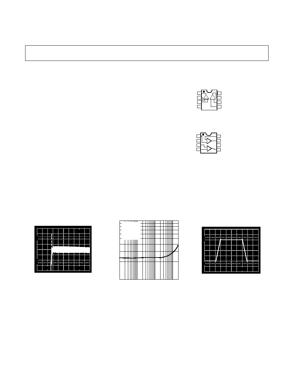
10
0%
100
90
500ns
10mV
870ns
Figure 1. Fast Settling (0.01%)
0.010
0.001
20
10k
100
1k
20k
T
A
= 25 C
V
S
= 15V
V
O
= 10V p-p
R
L
= 10k
A
V
= 1
Figure 2. Low Distortion A
V
= 1,
R
L
= 10 k
10
0%
100
90
1µs
5V
Figure 3. Excellent Output Drive,
R
L
= 600

≠2≠
REV. E
OP249≠SPECIFICATIONS
ELECTRICAL CHARACTERISTICS
OP249A
OP249F
Parameter
Symbol
Conditions
Min
Typ
Max
Min
Typ
Max
Unit
Offset Voltage
V
OS
0.2
0.5
0.2
0.7
mV
Long Term Offset Voltage
V
OS
(Note 1)
0.8
1.0
mV
Offset Stability
1.5
1.5
µV/Month
Input Bias Current
I
B
V
CM
= 0 V, T
J
= 25
∞C
30
75
30
75
pA
Input Offset Current
I
OS
V
CM
= 0 V, T
J
= 25
∞C
6
25
6
25
pA
Input Voltage Range
IVR
(Note 2)
12.5
12.5
V
±11
±11
V
≠12.5
≠12.5
V
Common-Mode Rejection
CMR
V
CM
=
±11 V
80
90
80
90
dB
Power-Supply Rejection Ratio
PSRR
V
S
=
±4.5 V to ±18 V
12
31.6
12
50
µV/V
Large-Signal Voltage Gain
A
VO
V
O
=
±10 V, R
L
= 2 k
1000
1400
500
1200
V/mV
Output Voltage Swing
V
O
R
L
= 2 k
12.5
12.5
V
±12.0
±12.0
V
≠12.5
≠12.5
V
Short-Circuit Current Limit
I
SC
Output Shorted to
36
36
mA
Ground
±20
±50
±20
±50
mA
≠33
≠33
mA
Supply Current
I
SY
No Load, V
O
= 0 V
5.6
7.0
5.6
7.0
mA
Slew Rate
SR
R
L
= 2 k
, C
L
= 50 pF
18
22
18
22
V/
µs
Gain-Bandwidth Product
GBW
(Note 3)
3.5
4.7
3.5
4.7
MHz
Settling Time
t
S
10 V Step 0.01%
4
0.9
1.2
0.9
1.2
µs
Phase Margin
0
0 dB Gain
55
55
Degrees
Differential Input Impedance
Z
IN
10
12
6
10
12
6
pF
Open-Loop Output Resistance
R
O
35
35
Voltage Noise
e
n
p-p
0.1 Hz to 10 Hz
2
2
µV p-p
Voltage Noise Density
e
n
f
O
= 10 Hz
75
75
nV/
Hz
f
O
= 100 Hz
26
26
nV/
Hz
f
O
= 1 kHz
17
17
nV/
Hz
f
O
= 10 kHz
16
16
nV/
Hz
Current Noise Density
i
n
f
O
= 1 kHz
0.003
0.003
pA/
Hz
Voltage Supply Range
V
S
±4.5
±15
±18
±4.5
±15
±18
V
NOTES
1
Long-term offset voltage is guaranteed by a 1000 HR life test performed on three independent wafer lots at 125
∞C with LTPD of three.
2
Guaranteed by CMR test.
3
Guaranteed by design.
4
Settling time is sample tested.
Specifications subject to change without notice.
ELECTRICAL CHARACTERISTICS
OP249G
Parameter
Symbol
Conditions
Min
Typ
Max
Unit
Offset Voltage
V
OS
0.4
2.0
mV
Input Bias Current
I
B
V
CM
= 0 V, T
J
= 25
∞C
40
75
pA
Input Offset Current
I
OS
V
CM
= 0 V, T
J
= 25
∞C
10
25
pA
Input Voltage Range
IVR
(Note 1)
12.5
V
±11
V
≠12.0
V
Common-Mode Rejection
CMR
V
CM
=
±11 V
76
90
dB
Power Supply Rejection Ratio
PSRR
V
S
=
±4.5 V to ±18 V
12
50
µV/V
Large Signal Voltage Gain
A
VO
V
O
=
±10 V; R
L
= 2 k
500
1100
V/mV
Output Voltage Swing
V
O
R
L
= 2 k
12.5
V
±12.0
V
≠12.5
V
Short-Circuit Current Limit
I
SC
Output Shorted to Ground
36
mA
±20
±50
mA
≠33
mA
Supply Current
I
SY
No Load; V
O
= 0 V
5.6
7.0
mA
Slew Rate
SR
R
L
= 2 k
, C
L
= 50 pF
18
22
V/
µs
Gain Bandwidth Product
GBW
(Note 2)
4.7
MHz
Settling Time
t
S
10 V Step 0.01%
0.9
1.2
µs
Phase Margin
0
0 dB Gain
55
Degree
Differential Input Impedance
Z
IN
10
12
6
pF
(@ V
S
= 15 V, T
A
= 25 C, unless otherwise noted.)
(@ V
S
= 15 V, T
A
= 25 C, unless otherwise noted.)

≠3≠
REV. E
OP249
OP249G
Parameter
Symbol
Conditions
Min
Typ
Max
Unit
Open Loop Output Resistance
R
O
35
Voltage Noise
e
n
p-p
0.1 Hz to 10 Hz
2
µV p-p
Voltage Noise Density
e
n
f
O
= 10 Hz
75
nV/
Hz
f
O
= 100 Hz
26
nV/
Hz
f
O
= 1 kHz
17
nV/
Hz
f
O
= 10 kHz
16
nV/
Hz
Current Noise Density
i
n
f
O
= 1 kHz
0.003
pA/
Hz
Voltage Supply Range
V
S
±4.5
±15
±18
V
NOTES
1
Guaranteed by CMR test.
2
Guaranteed by design.
Specifications subject to change without notice.
ELECTRICAL CHARACTERISTICS
OP249A
OP249F
Parameter
Symbol
Conditions
Min
Typ
Max
Min
Typ
Max
Unit
Offset Voltage
V
OS
0.12
1.0
0.5
1.1
mV
Offset Voltage Temperature
Coefficient
TCV
OS
1
5
2.2
6
µV/∞C
Input Bias Current
I
B
(Note 1)
4
20
0.3
4.0
nA
Input Offset Current
I
OS
(Note 1)
0.04
4
0.02
1.2
nA
Input Voltage Range
IVR
(Note 2)
12.5
12.5
V
±11
±11
V
≠12.5
≠12.5
V
Common-Mode Rejection
CMR
V
CM
=
±11 V
76
110
80
90
dB
Power-Supply Rejection Ratio
PSRR
V
S
=
±4.5 V to ±18 V
5
50
7
100
µV/V
Large-Signal Voltage Gain
A
VO
R
L
= 2 k
; V
O
=
±10 V
500
1400
250
1200
V/mV
Output Voltage Swing
V
O
R
L
= 2 k
12.5
12.5
V
±12
±12
V
≠12.5
≠12.5
V
Short-Circuit Current Limit
I
SC
Output Shorted to
Ground
±10
±60
±18
±60
mA
Supply Current
I
SY
No Load, V
O
= 0 V
5.6
7.0
5.6
7.0
mA
NOTES
1
T
J
= 85
∞C for F Grades; T
J
= 125
∞C for A Grade.
2
Guaranteed by CMR test.
Specifications subject to change without notice.
(@ V
S
= 15 V, ≠40 C
T
A
+85 C for F grades and ≠55 C T
A
+125 C for A grade
unless otherwise noted.)
ELECTRICAL CHARACTERISTICS
OP249G
Parameter
Symbol
Conditions
Min
Typ
Max
Unit
Offset Voltage
V
OS
1.0
3.6
mV
Offset Voltage Temperature
Coefficient
TCV
OS
6
25
µV/∞C
Input Bias Current
I
B
(Note 1)
0.5
4.5
nA
Input Offset Current
I
OS
(Note 1)
0.04
1.5
nA
Input Voltage Range
IVR
(Note 2)
12.5
V
±11
V
≠12.5
V
Common-Mode Rejection
CMR
V
CM
=
±11 V
76
95
dB
Power-Supply Rejection Ratio
PSRR
V
S
=
±4.5 V to ±18 V
10
100
µV/V
Large-Signal Voltage Gain
A
VO
R
L
= 2 k
; V
O
=
±10 V
250
1200
V/mV
Output Voltage Swing
V
O
R
L
= 2 k
12.5
V
±12.0
V
≠12.5
V
Short-Circuit Current Limit
I
SC
Output Shorted to Ground
±18
±60
mA
Supply Current
I
SY
No Load, V
O
= 0 V
5.6
7.0
mA
NOTES
1
T
J
= 85
∞C.
2
Guaranteed by CMR test.
Specifications subject to change without notice.
(@ V
S
= 15 V, ≠40 C
T
A
+85 C for unless otherwise noted.)
OP249
≠4≠
REV. E
ABSOLUTE MAXIMUM RATINGS
1
Supply Voltage . . . . . . . . . . . . . . . . . . . . . . . . . . . . . . .
±18 V
Input Voltage
2
. . . . . . . . . . . . . . . . . . . . . . . . . . . . . .
±18 V
Differential Input Voltage
2
. . . . . . . . . . . . . . . . . . . . . . . 36 V
Output Short-Circuit Duration . . . . . . . . . . . . . . . . Indefinite
Storage Temperature Range . . . . . . . . . . . . ≠65
∞C to +175∞C
Operating Temperature Range
OP249A (Z) . . . . . . . . . . . . . . . . . . . . . . . ≠55
∞C to +125∞C
OP249E, F (Z) . . . . . . . . . . . . . . . . . . . . . ≠40
∞C to +85∞C
OP249G (P, S) . . . . . . . . . . . . . . . . . . . . . ≠40
∞C to +85∞C
Junction Temperature
OP249 (Z) . . . . . . . . . . . . . . . . . . . . . . . . ≠65
∞C to +175∞C
OP249 (P, S) . . . . . . . . . . . . . . . . . . . . . . ≠65
∞C to +150∞C
Lead Temperature Range (Soldering, 60 sec) . . . . . . . 300
∞C
ORDERING GUIDE
*
Model
Temperature Range
Package Descriptions
Package Options
OP249AZ
≠55
∞C to +125∞C
8-Lead Cerdip
Q-8
OP249FZ
≠40
∞C to +85∞C
8-Lead Cerdip
Q-8
OP249GP
≠40
∞C to +85∞C
8-Lead Plastic DIP
N-8
OP249GS
*
≠40
∞C to +85∞C
8-Lead SO
SO-8
OP249GS-REEL
≠40
∞C to +85∞C
8-Lead SO
SO-8
OP249GS-REEL7
≠40
∞C to +85∞C
8-Lead SO
SO-8
NOTES
*For availability and burn-in information on SO and PLCC packages, contact your local sales office.
For Military processed devices, please refer to the Standard Microcircuit Drawing (SMD) available at
www.dscc.dla.mil/programs/milspec/default.asp
CAUTION
ESD (electrostatic discharge) sensitive device. Electrostatic charges as high as 4000 V readily
accumulate on the human body and test equipment and can discharge without detection. Although
the OP249 features proprietary ESD protection circuitry, permanent damage may occur on
devices subjected to high-energy electrostatic discharges. Therefore, proper ESD precautions are
recommended to avoid performance degradation or loss of functionality.
WARNING!
ESD SENSITIVE DEVICE
Package Type
JA
3
JC
Unit
8-Lead Hermetic DIP (Z)
134
12
∞C/W
8-Lead Plastic DIP (P)
96
37
∞C/W
8-Lead SO (S)
150
41
∞C/W
NOTES
1
Absolute maximum ratings apply to packaged parts, unless otherwise noted.
2
For supply voltages less than
± 18 V, the absolute maximum input voltage is equal
to the supply voltage.
3
JA
is specified for worst-case mounting conditions, i.e.,
JA
is specified for device
in socket for cerdip and P-DIP packages;
JA
is specified for device soldered to
printed circuit board for SO package.
SMD Part Number
ADI Equivalent
5962-9151901M2A
OP249ARCMDA
5962-9151901MGA
OP249AJMDA
5962-9151901MPA
OP249AZMDA
OP249
≠5≠
REV. E
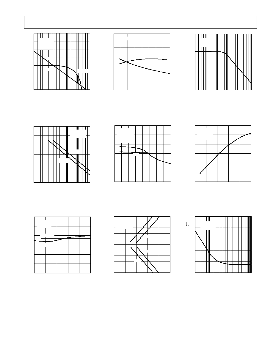
Typical Performance Characteristics≠
FREQUENCY ≠ Hz
OPEN-LOOP GAIN
≠
dB
120
1k
100
80
60
40
20
0
≠20
10k
100k
1M
10M
100M
0
45
90
135
180
225
T
A
= 25 C
V
S
= 15V
R
L
= 2k
m = 55
GAIN
PHASE
PHASE
≠
C
TPC 1. Open-Loop Gain, Phase vs.
Frequency
FREQUENCY ≠ Hz
POWER SUPPLY REJECTION
≠
dB
1k
120
100
80
60
40
20
0
10k
100k
1M
T
A
= 25 C
V
S
= 15V
100
10
≠PSRR
+PSRR
TPC 4. Power Supply Rejection vs.
Frequency
CAPACITIVE LOAD ≠ pF
SLEW RATE
≠
V/
s
35
30
0
25
T
A
= 25 C
V
S
= 15V
20
15
10
5
100
200
300
400
500
NEGATIVE
POSITIVE
TPC 7. Slew Rate vs. Capacitive
Load
TEMPERATURE ≠ C
PHASE MARGIN
≠
C
65
60
45
≠75
55
50
≠50
≠25
0
25
50
75
100 125
GAIN BANDWIDTH PRODUCT
≠
MHz
10
8
2
6
4
V
S
= 15V
GBW
m
TPC 2. Gain Bandwidth Product,
Phase Margin vs. Temperature
TEMPERATURE ≠ C
SLEW RATE
≠
V/
s
28
26
≠75
24
≠50
≠25
0
25
50
75
100 125
V
S
= 15V
R
L
= 2k
C
L
= 50pF
+SR
≠SR
22
20
18
16
TPC 5. Slew Rate vs. Temperature
0.1%
SETTLING TIME ≠ ns
OUTPUT STEP SIZE
≠
Volts
0
T
A
= 25 C
V
S
= 15V
A
VCL
= 1
≠10
200
400
600
800
1000
0.01%
≠8
≠6
≠4
≠2
0
2
4
6
8
10
0.1%
0.01%
TPC 8. Settling Time vs. Step Size
FREQUENCY ≠ Hz
COMMON-MODE REJECTION
≠
dB
140
1k
120
100
80
60
40
20
0
10k
100k
1M
10M
T
A
= 25 C
V
S
= 15V
100
TPC 3. Common-Mode Rejection vs.
Frequency
DIFFERENTIAL INPUT VOLTAGE ≠ Volts
SLEW RATE
≠
V/
s
28
26
0
24
T
A
= 25 C
V
S
= 15V
R
L
= 2k
22
20
18
16
0.2
0.4
0.6
0.8
1.0
TPC 6. Slew Rate vs. Differential
Input Voltage
FREQUENCY ≠ Hz
100
0
100
80
60
40
20
0
T
A
= 25 C
V
S
= 15V
1k
10k
VOLTAGE NOISE DENSITY
≠
nV
Hz
TPC 9. Voltage Noise Density vs.
Frequency