 | –≠–ª–µ–∫—Ç—Ä–æ–Ω–Ω—ã–π –∫–æ–º–ø–æ–Ω–µ–Ω—Ç: OP290E | –°–∫–∞—á–∞—Ç—å:  PDF PDF  ZIP ZIP |

REV. A
Information furnished by Analog Devices is believed to be accurate and
reliable. However, no responsibility is assumed by Analog Devices for its
use, nor for any infringements of patents or other rights of third parties that
may result from its use. No license is granted by implication or otherwise
under any patent or patent rights of Analog Devices.
a
OP290
One Technology Way, P.O. Box 9106, Norwood, MA 02062-9106, U.S.A.
Tel: 781/329-4700
www.analog.com
Fax: 781/326-8703
© Analog Devices, Inc., 2002
Precision, Low Power, Micropower
Dual Operational Amplifier
PIN CONNECTIONS
16-Lead SOL
(S-Suffix)
TOP VIEW
(Not to Scale)
16
15
14
13
12
11
10
9
1
2
3
4
5
6
7
8
NC = NO CONNECT
≠IN A
OP290
+IN A
NC
V≠
NC
+IN B
≠IN B
NC
+IN A
NC
NC
V+
NC
NC
OUT B
NC
EPOXY MINI-DIP
(P-Suffix)
8-Lead HERMETIC DIP
(Z-Suffix)
8
7
6
5
1
2
3
4
OP290
A
B
OUT A
≠IN A
+IN A
V≠
V+
OUT B
≠IN B
+IN B
FEATURES
Single-/Dual-Supply Operation, 1.6 V to 36 V, 0.8 V to 18 V
True Single-Supply Operation; Input and Output Voltage
Ranges Include Ground
Low Supply Current (Per Amplifier), 20 A Max
High Output Drive, 5 mA Min
Low Input Offset Voltage, 200 V Max
High Open-Loop Gain, 700 V/mV Min
Outstanding PSRR, 5.6 V/V Max
Industry Standard 8-Lead Dual Pinout
Available in Die Form
GENERAL DESCRIPTION
The OP290 is a high performance micropower dual op amp that
operates from a single supply of 1.6 V to 36 V or from dual
supplies of
±0.8 V to ±18 V. Input voltage range includes the
negative rail allowing the OP290 to accommodate input signals
down to ground in single-supply operation. The OP290's out-
put swing also includes ground when operating from a single
supply, enabling "zero-in, zero-out" operation.
The OP290 draws less than 20
µA of quiescent supply current
per amplifier, while able to deliver over 5 mA of output current
to a load. Input offset voltage is below 200
µV eliminating the
need for external nulling. Gain exceeds 700,000 and common-mode
rejection is better than 100 dB. The power supply rejection ratio
of under 5.6 pV/V minimizes offset voltage changes experienced
in battery-powered systems. The low offset voltage and high gain
offered by the OP290 bring precision performance to micropower
applications. The minimal voltage and current requirements
of the OP290 suit it for battery- and solar-powered applications,
such as portable instruments, remote sensors, and satellites. For
a single op amp, see the OP90; for a quad, see the OP490.
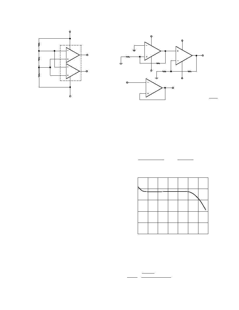
+IN
≠IN
NULL
NULL
OUTPUT
V+
V
ELECTRONICALLY ADJUSTED ON CHIP
FOR MINIMUM OFFSET VOLTAGE
Figure 1. Simplified Schematic (one of two amplifiers is shown)

REV. A
≠2≠
OP290≠SPECIFICATIONS
(@ V
S
= 1.5 V to 15 V, T
A
= 25 C, unless otherwise noted.)
ELECTRICAL CHARACTERISTICS
OP290E
OP290F
OP290G
Parameter
Symbol
Conditions
Min
Typ Max Min
Typ
Max Min
Typ
Max Unit
INPUT OFFSET VOLTAGE
V
OS
50
200
75
300
125
500
µV
INPUT OFFSET CURRENT
I
OS
V
CM
= 0 V
0.1
3
0.1
5
0.1
5
nA
INPUT BIAS CURRENT
I
B
V
CM
= 0 V
4.0
15
4.0
20
4.0
25
nA
LARGE-SIGNAL
A
VO
V
S
=
±15 V, V
O
=
±10 V
VOLTAGE GAIN
R
L
= 100 k
700
1200
500
1000
400
600
R
L
= 10 k
350
600
250
500
200
400
R
L
= 2 k
125
250
100
200
100
200
V/mV
V+ = 5V, V≠ = 0 V,
1 V < V
O
< 4 V
R
L
= 100 k
200
400
125
300
100
250
R
L
= 10 k
100
180
75
140
70
140
INPUT VOLTAGE RANGE
1
IVR
V+ = 5 V, V≠ = 0 V
0/4
0/4
0/4
V
V
S
=
±5 V
1
≠15/13.5
≠15/13.5
≠15/13.5
OUTPUT VOLTAGE SWING
V
O
V
S
=
±5 V
R
L
= 10 k
±13.5±14.2
±13.5±14.2
±13.5 ±14.2 V
R
L
= 2 k
±10.5±11.5
±10.5±11.5
±10.5 ±11.5
V
OH
V+ = 5 V, V≠ = 0 V
40
4.2
4.0
4.2
4.0
4.2
V
V+ = 5 V, V≠ = 0 V
V
OL
R
L
= 10kn
10
50
10
50
10
50
µV
COMMON-MODE
CMR
V+ = 5 V, V≠ = 0 V
ttS
80
100
80
100
dB
REJECTION
0 V < V
CM
< 4 V
V
S
=
±15 V,
100
120
90
120
90
120
≠15 V < V
CM
< 13.5 V
POWER SUPPLY
PSRR
10
5.6
10
5.6
3.2
10
µV/V
REJECTION RATIO
SUPPLY CURRENT
I
SY
V
S
=
±1.5 V
19
30
19
30
19
30
µA
(All Amplifiers)
V
S
=
±15 V
25
40
25
40
25
40
CAPACITIVE LOAD
A
V
= +1
650
650
650
PF
STABILITY
No Oscillations
INPUT NOISE VOLTAGE
1
e
np-p
f
O
= 0.1 Hz to 10 Hz
3
3
3
µV
p-p
V
S
=
±15 V
INPUT RESISTANCE
DIFFERENTIAL-MODER
IN
V
S
=
±15 V
30
30
30
M
INPUT RESISTANCE
R
INCM
V
S
=
±15 V
20
20
20
G
COMMON-MODE
SLEW RATE
SR
A
V
= +1
5
12
5
12
5
12
V/ms
V
S
=
±15 V
GAIN BANDWIDTH
GBWP
Vs = +15 V
20
20
20
kHz
PRODUCT
V
S
=
±15 V
CHANNEL
SEPARATION
2
CS
f
O
= 10 Hz
120
150
120
150
120
150
dB
V
O
= 20 Vp-p
V
S
=
±15 V
2
NOTES
1
Guaranteed by CMR test.
2
Guaranteed but not 100% tested.
Specifications subject to change without notice.

REV. A
≠3≠
OP290
ELECTRICAL CHARACTERISTICS
(@ V
S
= 1.5 V to 15 V, ≠55 C
T
A
125 C, unless otherwise noted.)
OP290A
Parameter
Symbol
Conditions
Min
Typ
Max
Unit
INPUT OFFSET VOLTAGE
V
OS
80
500
µV
AVERAGE INPUT OFFSET
VOLTAGE DRIFT
TCV
OS
V
S
= 15 V
0 3
3
µV/∞C
INPUT OFFSET CURRENT
I
OS
VCM = 0 V
0.1
5
nA
INPUT BIAS CURRENT
I
B
VCM = 0 V
4.2
20
nA
LARGE-SIGNAL
V
S
= 15 V, V
O
=
±10 V
VOLTAGE GAIN
R
L
= 100 k
225
400
R
L
= 10 k
125
240
A
VO
R
L
= 2 k
50
110
V+ = 5 V, V≠ = 0 V,
V/mV
1 V < V
O
< 4 V
R
L
= 100 k
100
200
R
L
= 10 k
50
110
INPUT VOLTAGE RANGE
*
IVR
V+ = 5 V, V≠ = 0 V
0/3.5
V
V
S
=
±15 V
*
≠15/13.5
OUTPUT VOLTAGE SWING
V
O
V
S
=
±15 V
R
L
= 10 k
±13
±14.1
V
R
L
= 2 k
±10
±11
V
OH
V+ = 5 V, V≠ = 0 V
R
L
= 2 k
V
V
OL
V+ = 5 V, V≠ = 0 V
10
100
µV
R
L
= 10 k
COMMON-MODE REJECTION
CMR
V+ = 5 V, V≠ = 0 V, 0 V < V
CM
< 13.5 V
80
105
dB
V
S
=
±15 V, ≠15 V < V
CM
< 13.5 V
90
115
POWER SUPPLY
PSRR
3.2
10
µV/V
REJECTION RATIO
SUPPLY CURRENT
V
S
=
±1.5 V
30
50
µA
(All Amplifiers)
IsY
V
S
=
±15 V
38
60
NOTES
*
Guaranteed by CMR test.
Specifications subject to change without notice.

REV. A
OP290
≠4≠
(@ V
S
= 1.5 V to 15 V, ≠40
C
T
A
85 C for OP290E/OP290F/OP290G, unless
otherwise noted.)
ELECTRICAL CHARACTERISTICS
OP290E
OP290F
OP290G
Parameter
Symbol Conditions
Min
Typ Max
Min
Typ Max
Min
Typ Max Unit
INPUT OFFSET VOLTAGE
V
OS
70
400
115
600
200
750
µV
AVERAGE INPUT OFFSET
VOLTAGE DRIFT
TCV
OS
V
S
=
±15 V
0.3
3
0.6
5
1.2
µV/∞C
INPUT OFFSET CURRENT
I
OS
V
CM
= 0 V
01
3
0.1
5
0.1
7
nA
INPUT BIAS CURRENT
I
B
V
CM
= 0 V
4.2
t5
4.2
20
4.2
25
nA
LARGE-SIGNAL
A
VO
V
S
=
±5 V, V
O
=
±0 V
V/mV
VOLTAGE GAIN
R
L
= 100 k
500
800
350
700
300
600
R
L
= 10 k
250
400
175
350
150
250
R
L
= 2 k
100
200
75
150
75
125
V+ = 5 V, V≠ = 0 V,
1 V < V
O
< 4 V
R
L
= 100 k
150
280
100
220
80
160
R
L
= 10 k
75
140
50
110
40
90
INPUT VOLTAGE RANGE
*
IVR
V+ = 5 V, V≠ = 0 V
0/3.5
0/3.5
0/3.5
V
V
S
= +15 V
*
≠15/13.5
≠15/13.5
≠15/13.5
OUTPUT VOLTAGE SWING
V
O
V
S
=
±15 V
R
L
= 10 k
±13
±14
±13
±14
±13
±14
V
R
L
= 2 k
±10
±11
±10
±11
±10
±11
V
OH
V+ = 5 V, V≠ = 0 V
R
L
= 2 k
3.9
4.1
3.9
4.1
3.9
4.1
V
V
OL
V+ = 5 V, V≠ = 0 V
R
L
= 10 k
10
100
10
100
10
100
µV
COMMON-MODE
CMR
V+ = 5 V, V≠ = 0 V,
85
105
80
100
80
100
dB
REJECTION
0 V < V
CM
< 3.5 V
V
S
=
±15 V
≠15 V < V
CM
< 13.5 V
95
115
90
110
90
110
POWER SUPPLY
PSRR
3.2
7.5
5.6
10
5.6
15
µV/V
REJECTION RATIO
SUPPLY CURRENT I
SY
V
S
=
±1.5 V
24
50
24
50
24
50
µA
(All Amplifiers)
V
S
=
±15 V
31
60
31
60
31
60
NOTE
*
Guaranteed by CMR test.
Specifications subject to change without notice.

REV. A
OP290
≠5≠
CAUTION
ESD (electrostatic discharge) sensitive device. Electrostatic charges as high as 4000 V readily
accumulate on the human body and test equipment and can discharge without detection. Although
the OP290 features proprietary ESD protection circuitry, permanent damage may occur on devices
subjected to high-energy electrostatic discharges. Therefore, proper ESD precautions are
recommended to avoid performance degradation or loss of functionality.
WARNING!
ESD SENSITIVE DEVICE
ABSOLUTE MAXIMUM RATINGS
1
Supply Voltage . . . . . . . . . . . . . . . . . . . . . . . . . . . . . . .
±18 V
Differential Input Voltage . . . [(V≠) ≠ 20 V] to [(V+) + 20 V]
Common-Mode Input Voltage . [(V≠) ≠ 20 V] to [(V+) + 20 V]
Output Short-Circuit Duration . . . . . . . . . . . . . . . . Indefinite
Storage Temperature Range
P, S, Z Packages . . . . . . . . . . . . . . . . . . . . . ≠65
∞C to +150∞C
Operating Temperature Range
OP290A . . . . . . . . . . . . . . . . . . . . . . . . . . . . ≠55
∞C to +125∞C
OP290E, OP290F, OP290G . . . . . . . . . . . . . ≠40
∞C to +85∞C
Junction Temperature (T
j
) . . . . . . . . . . . . . ≠65
∞C to +150∞C
Lead Temperature Range (Soldering, 60 sec) . . . . . . . 300
∞C
Package Type
jA
2
jC
Unit
8-Lead Hermetic DIP (Z)
134
12
∞C/W
8-Lead Plastic DIP (P)
96
37
∞C/W
16-Lead SOL (S)
92
27
∞C/W
NOTES
1
Absolute Maximum Ratings apply to both DICE and packaged parts, unless
otherwise noted.
2
jA
is specified for worst-case mounting conditions, i.e.,
jA
is specified for
device in socket for CERDIP and P-DIP packages;
jA
is specified for device
soldered to printed circuit board for SOL package.
ORDERING GUIDE
T
A
= 25 C
Package
Operating
V
OS
Max
Cerdip
Temperature
(mV)
8-Lead
Plastic
Range
200
OP290AZ
*
MIL
200
OP290EZ
*
XIND
300
OP290FZ
*
XIND
500
OP290GP
XIND
500
OP290GS
*
XIND
*Not for new designs. Obsolete April 2002.
For military processed devices, please refer to the Standard
Microcircuit Drawing (SMD) available at
www.dscc.dla.mil/programs.milspec./default.asp
SMD Part Number
ADI Part Number
5962-89783012A
*
OP290ARCMDA
5962-8978301PA
*
OP290AZMDA
*Not for new designs. Obsolete April 2002.
REV. A
OP290
≠6≠
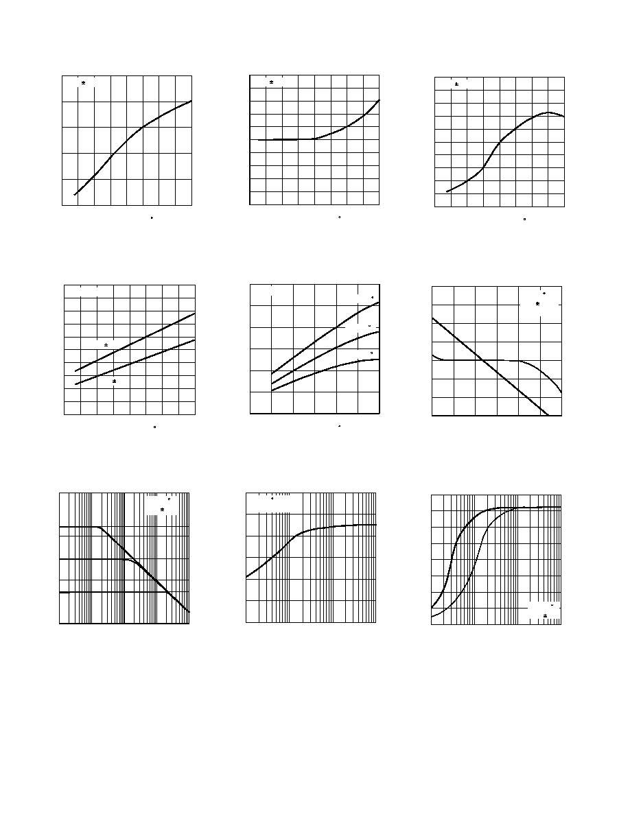
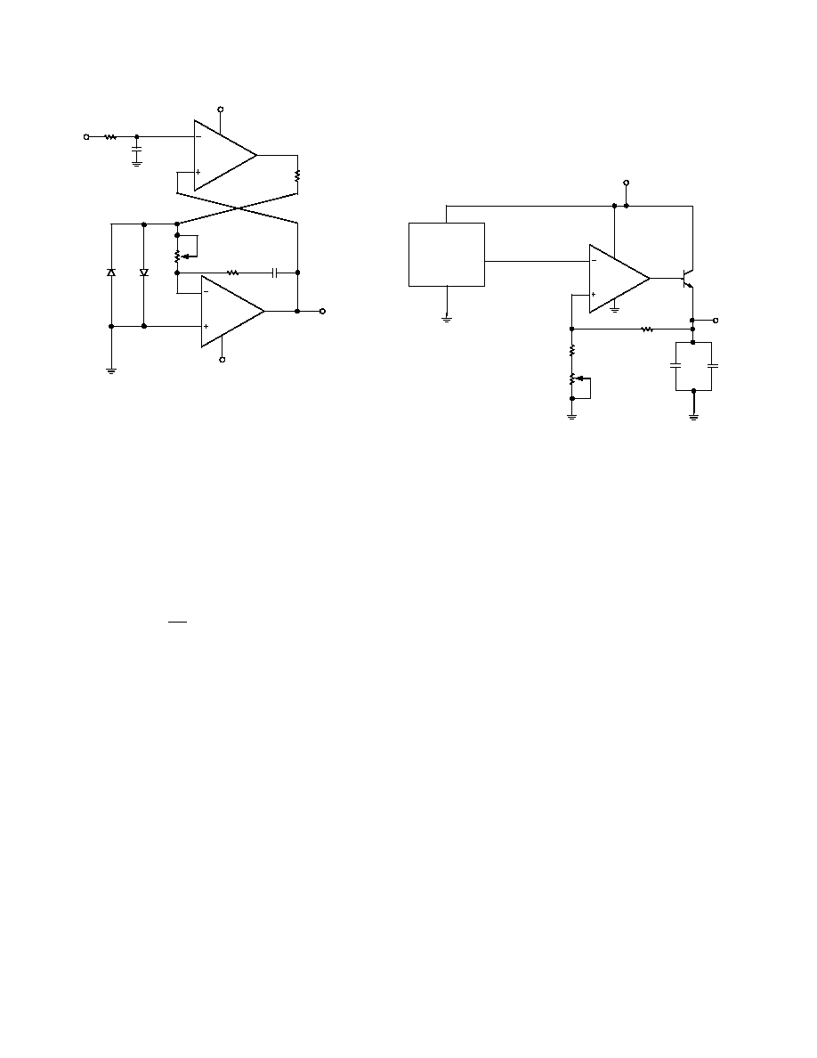
TEMPERATURE ≠ C
INPUT OFFSET VOLTAGE
≠
V
100
80
0
≠75
60
40
20
125
100
75
50
≠50
≠25
0
25
V
S
= 15V
TPC 1. Input Offset Voltage vs.
Temperature
TEMPERATURE ≠ C
SUPPLY CURRENT
≠
A
32
4
≠75
24
16
125
100
75
50
≠50
≠25
0
25
NO LOAD
40
36
28
20
12
8
V
S
= 15V
V
S
= 1.5V
44
TPC 4. Supply Current vs.
Temperature
FREQUENCY ≠ Hz
CLOSED-LOOP GAIN
≠
dB
60
40
≠20
10
100
100k
1k
10k
20
0
T
A
= 25 C
V
s
= 15V
TPC 7. Closed-Loop Gain vs.
Frequency
TEMPERATURE ≠ C
INPUT OFFSET CURRENT
≠
nA
0.14
0.12
0.06
≠75
0.1
0.08
125
100
75
50
≠50
≠25
0
25
V
S
= 15V
TPC 2. Input Offset Current vs.
Temperature
TEMPERATURE ≠ C
OPEN-LOOP GAIN
≠
V/mV
600
0
0
500
300
30
25
20
15
5
10
400
200
100
T
A
= 25 C
R
L
= 10k
T
A
= 85 C
T
A
= 125 C
TPC 5. Open-Loop Gain vs.
Single-Supply Voltage
LOAD RESISTANCE ≠
OUTPUT VOLTAGE SWING
≠
V
6
0
100k
3
100
1k
10k
5
4
2
1
T
A
= 25 C
V+ = 5V, V≠ = 0V
TPC 8. Ouput Voltage Swing vs.
Load Resistance
TEMPERATURE ≠ C
INPUT BIAS CURRENT
≠
nA
4.5
4.2
3.5
≠75
4.0
3.8
125
100
75
50
≠50
≠25
0
25
V
S
= 15V
4.4
4.3
4.1
3.9
3.7
3.6
TPC 3. Input Bias Current vs.
Temperature
FREQUENCY ≠ Hz
OPEN-LOOP GAIN
≠
dB
140
0
0
120
80
30
25
20
15
5
10
100
60
40
T
A
= 25 C
V
s
= 15V
R
L
= 100k
GAIN
PHASE SHIFT
≠
Degrees
20
TPC 6. Open-Loop Gain and Phase
Shift vs. Frequency
LOAD RESISTANCE ≠
OUTPUT VOLTAGE SWING
≠
V
16
0
100k
10
100
1k
10k
14
12
8
4
T
A
= 25 C
V
s
= 15V
2
6
TPC 9. Output Voltage Swing
vs. Load Resistance

REV. A
≠7≠
Typical Performance Characteristics≠OP290
FREQUENCY ≠ Hz
POWER SUPPLY REJECTION
≠
dB
140
40
1k
1
10
100
120
100
80
T
A
= 25 C
60
POSITIVE SUPPLY
NEGATIVE SUPPLY
TPC 10. Power Supply Rejection
vs. Frequency
FREQUENCY ≠ Hz
CURRENT NOISE DESTINY
≠
nV/
Hz
10
1
0.1
0.1
1
1k
10
100
T
A
= 25 C
V
S
= 15V
TPC 13. Current Noise Density
vs. Frequency
FREQUENCY ≠ Hz
COMMON MODE REJECTION
≠
dB
140
40
1k
1
10
100
120
100
80
T
A
= 25 C
V
S
= 15V
60
TPC 11. Common-Mode Rejection
vs. Frequency
10
0%
100
90
100 s
20mV
T
A
= 25 C
V
S
= 15V
A
V
= +1
R
L
= 10k
C
L
= 500pF
TPC 14. Small-Signal Transient
Response
FREQUENCY ≠ Hz
NOISE VOLTAGE DESTINY
≠
nV/
Hz
1,000
100
10
0.1
1
1k
10
100
T
A
= 25 C
V
S
= 15V
TPC 12. Noise Voltage Density
vs. Frequency
10
0%
100
90
1ms
5V
T
A
= 25 C
V
S
= 15V
A
V
= +1
R
L
= 10k
C
L
= 500pF
TPC 15. Large-Signal Transient
Response
REV. A
OP290
≠8≠
1
7
4
5
6
3
2
8
+18V
≠18V
100k
200
100k
1/2
OP290
1/2
OP290
Figure 2. Burn-In Circuit
APPLICATIONS INFORMATION
BATTERY-POWERED APPLICATIONS
The OP290 can be operated on a minimum supply voltage of
1.6 V, or with dual supplies of 0.8 V, and draws only 19 pA of
supply current. In many battery-powered circuits, the OP290
can be continuously operated for thousands of hours before
requiring battery replacement, reducing equipment downtime
and operating cost.
High-performance portable equipment and instruments fre-
quently use lithium cells because of their long shelf-life, light
weight, and high energy density relative to older primary cells.
Most lithium cells have a nominal output voltage of 3 V and are
noted for a flat discharge characteristic. The low supply voltage
requirement of the OP290, combined with the flat discharge
characteristic of the lithium cell, indicates that the OP290 can
be operated over the entire useful life of the cell. Figure 1 shows
the typical discharge characteristic of a 1 Ah lithium cell power-
ing an OP290 with each amplifier, in turn, driving full output
swing into a 100 k
load.
INPUT VOLTAGE PROTECTION
The OP290 uses a PNP input stage with protection resistors in
series with the inverting and noninverting inputs. The high
breakdown of the PNP transistors coupled with the protection
resistors provide a large amount of input protection, allowing
the inputs to be taken 20 V beyond either supply without dam-
aging the amplifier.
SINGLE-SUPPLY OUTPUT VOLTAGE RANGE
In single-supply operation the OP290's input and output ranges
include ground. This allows true "zero-in, zero-out" operation.
The output stage provides an active pull-down to around 0.8 V
above ground. Below this level, a load resistance of up to 1 MS2
to ground is required to pull the output down to zero.
In the region from ground to 0.8 V, the OP290 has voltage gain
equal to the data sheet specification. Output current source capa-
bility is maintained over the entire voltage range including ground.
+15V
+15V
≠15V
≠15V
V2
V
IN
1k
9k
100
10k
V1 20Vp-p @ 10Hz
CHANNEL SEPARATION = 20 LOG
V1
V2/1000
1/2
OP290
A
1/2
OP290
B
OP37A
Figure 3. Channel Separation Test Circuit
APPLICATIONS
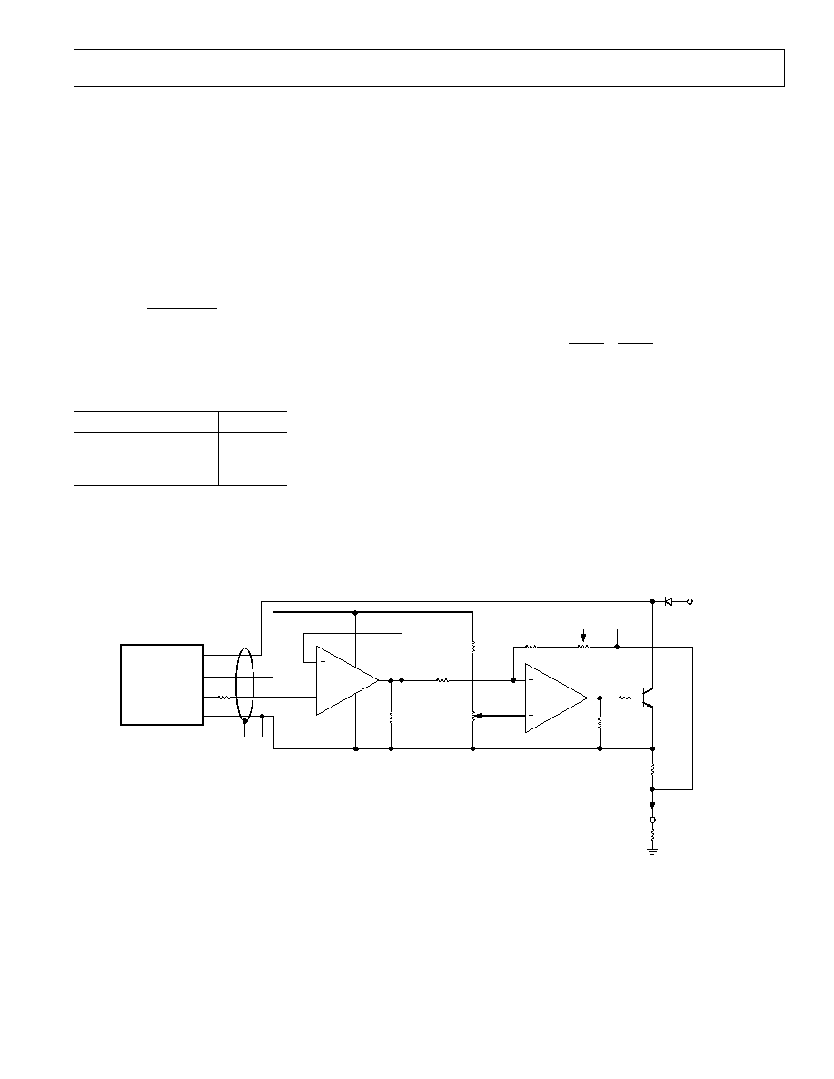
TEMPERATURE TO 4≠20 mA TRANSMITTER
A simple temperature to 4≠20 mA transmitter is shown in Figure 5.
After calibration, the transmitter is accurate to +0.5
∞C over the
≠50
∞C to +150∞C temperature range. The transmitter operates
from 8 V to 40 V with supply rejection better than 3 ppm/V.
One half of the OP290 is used to buffer the V
TEMP
pins while
the other half regulates the output current to satisfy the current
summation at its noninverting input.
I
V
R
R
R R
V
R R R
R R
OUT
TEMP
SET
=
+
(
)
6
7
2 10
2 6
7
2 10
≠
LITHIUM SULPHUR DIOXIDE
CELL VOLTAGE
≠
V
100
80
0
0
60
40
20
3500
3000
2500
500
1000
2000
1500
HOURS
Figure 4. Lithium Sulphur Dioxide Cell Discharge
Characteristic with OP290 and 100 k Loads
The change in output current with temperature is the derivative
of the transfer function:
I
T
V
T
R
R
R R
OUT
TEMP
=
+
(
)
6
7
2 10
REV. A
OP290
≠9≠
From the formulas, it can be seen that if the span trim is adjusted
before the zero trim, the two trims are not interactive, which
greatly simplifies the calibration procedure.
Calibration of the transmitter is simple. First, the slope of the
output current versus temperature is calibrated by adjusting the
span trim, R7. A couple of iterations may be required to be sure
the slope is correct.
Once the span trim has been completed, the zero trim can be made.
Remember that adjusting the offset trim will not affect the gain.
The offset trim can be set at any known temperature by adjusting
R
5
until the output current equals:
I
I
T
T
T
mA
OUT
FS
OPERATING
AMBIENT
MIN
=
(
)
+
≠
4
Table I shows the values of R6 required for various tempera-
ture ranges.
VARIABLE SLEW RATE FILTER
The circuit shown in Figure 6 can be used to remove pulse noise
from an input signal without limiting the response rate to a genu-
ine signal. The nonlinear filter has use in applications where
the input signal of interest is known to have physical limitations.
An example of this is a transducer output where a change of
temperature or pressure cannot exceed a certain rate due to
physical limitations of the environment. The filter consists of a
comparator which drives an integrator. The comparator com-
pares the input voltage to the output voltage and forces the
integrator output to equal the input voltage. A1 acts as a com-
parator with its output high or low. Diodes D1 and D2 clamp
the voltage across R3 forcing a constant current to flow in or
out of C2. R3, C2, and A2 form an integrator with A2's output
slewing at a maximum rate of:
Maximum slew rate
V
R C
V
R C
D
=
3 2
0 6
3 2
.
For an input voltage slewing at a rate under this maximum slew
rate, the output simply follows the input with A1 operating in its
linear region.
1/2
OP290EZ
V
IN
V
OUT
V
TEMP
GND
6
3
2
4
R1
10k
REF-43BZ
2N1711
V+
8V TO 40V
1N4002
SPAN TRIM
R10
100
1%, 1/2W
R9
100k
R8
1k
R3
100k
R5
5k
R2
1k
V
TEMP
4
8
2
ZERO
TRIM
V
SET
R4
20k
R6
3k
R7
5k
I
OUT
R
LOAD
7
6
5
1
1/2
OP290EZ
Figure 5. Temperature to 4-20 mA Transmitter
Table I.
Temperature Range
R6 (k )
0
∞C to +70∞C
10
≠40
∞C to +85∞C
6.2
≠55
∞C to +150∞C
3
REV. A
OP290
≠10≠
1/2
OP290GP
1
1/2
OP290GP
3
2
7
6
5
R1
250k
C
1
0.1 F
+15V
≠15V
V
OUT
R2
100k
R3
1M
D
2
D
1
DIODES ARE 1N4148
4
R4
25k
C
1
4700pF
8
Figure 6. Variable Slew Rate Filter
LOW OVERHEAD VOLTAGE REFERENCE
Figure 7 shows a voltage reference that requires only 0.1 V of
overhead voltage. As shown, the reference provides a stable
4.5 V output with a 4.6 V to 36 V supply. Output voltage drift is
only 12 ppm/
∞C. Line regulation of the reference is under 5 HV/V
with load regulation better than 10
µV/mA with up to 50 mA of
output current.
The REF-43 provides a stable 2.5 V which is multiplied by the
OP290. The PNP output transistor enables the output voltage
to approach the supply voltage.
Resistors R1 and R2 determine the output voltage.
V
V
R
R
OUT
=
+
2 5
1
2
1
.
The 200
variable resistor is used to trim the output voltage.
For the lowest temperature drift, parallel resistors can be used in
place of the variable resistor and taken out of the circuit as required
to adjust the output voltage.
6
2
4
REF-43FZ
R1B
200
20-TURN
BOURNS 3006P-1-201
V
OUT
V
IN
V
OUT
GND
R1A
2.37
1%
C
1
10 F
C2
0.1 F
V+
R2
2k
1%
2N2907A
1
1/2
OP290GP
3
2
8
4
Figure 7. Low Overhead Voltage Reference

REV. A
OP290
≠11≠
Revision History
Location
Page
Data Sheet changed from REV. 0 to REV. A.
Edits to ORDERING INFORMATION . . . . . . . . . . . . . . . . . . . . . . . . . . . . . . . . . . . . . . . . . . . . . . . . . . . . . . . . . . . . . . . . . . . . . . 1
Edits to PIN CONNECTIONS . . . . . . . . . . . . . . . . . . . . . . . . . . . . . . . . . . . . . . . . . . . . . . . . . . . . . . . . . . . . . . . . . . . . . . . . . . . . . 1
Edits to ABSOLUTE MAXIMUM RATINGS . . . . . . . . . . . . . . . . . . . . . . . . . . . . . . . . . . . . . . . . . . . . . . . . . . . . . . . . . . . . . . . . . 2
Edits to PACKAGE TYPE . . . . . . . . . . . . . . . . . . . . . . . . . . . . . . . . . . . . . . . . . . . . . . . . . . . . . . . . . . . . . . . . . . . . . . . . . . . . . . . . 2
Edits to WAFER TEST LIMITS . . . . . . . . . . . . . . . . . . . . . . . . . . . . . . . . . . . . . . . . . . . . . . . . . . . . . . . . . . . . . . . . . . . . . . . . . . . 5
Edits to DICE CHARACTERISTICS . . . . . . . . . . . . . . . . . . . . . . . . . . . . . . . . . . . . . . . . . . . . . . . . . . . . . . . . . . . . . . . . . . . . . . . 5

≠12≠
C00327≠0≠1/02(A)
PRINTED IN U.S.A.