 | –≠–ª–µ–∫—Ç—Ä–æ–Ω–Ω—ã–π –∫–æ–º–ø–æ–Ω–µ–Ω—Ç: OP420H | –°–∫–∞—á–∞—Ç—å:  PDF PDF  ZIP ZIP |
OP420 Data Sheet
REV. A
Information furnished by Analog Devices is believed to be accurate and
reliable. However, no responsibility is assumed by Analog Devices for its
use, nor for any infringements of patents or other rights of third parties that
may result from its use. No license is granted by implication or otherwise
under any patent or patent rights of Analog Devices.
a
OP420
One Technology Way, P.O. Box 9106, Norwood, MA 02062-9106, U.S.A.
Tel: 781/329-4700
www.analog.com
Fax: 781/326-8703
© Analog Devices, Inc., 2002
Quad Micropower
Operational Amplifier
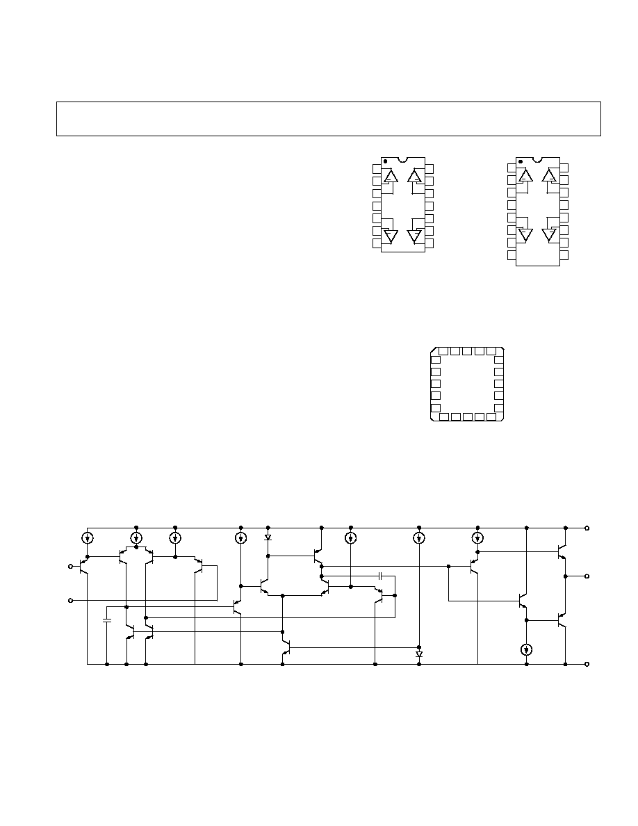
PIN CONNECTIONS
GENERAL DESCRIPTION
The OP420 quad micropower operational amplifier is a single-
chip quad patterned after the OP20 precision micropower single
operational amplifier. A Darlington PNP input stage allows the
input common-mode voltage to include V≠. The wide input
range combined with low power supply drain (~40
µA/section at
5 V) provides a unique solution for designs requiring high func-
tional density and portable operation. Applications include
2-wire transmitters for process control loops, battery-operated
remote-line filters, signal preconditioning amplifiers, and a
variety of multiple-gain block arrays.
≠IN
≠IN
Q1
Q3
Q4
C1
Q5
Q6
Q2
Q7
Q9
Q11
Q10
Q13
Q8
Q12
Q33
Q26
Q27
Q29
V≠
OUTPUT
V+
Q28
Figure 1. Simplified Schematic (1/4 Shown)
FEATURES
Low Supply Current: 200 A Max @ V
S
= 5 V
Single-Supply Operation: 5 V to 30 V
Dual-Supply Operation: 2.5 V to 15 V
Low Input Offset Voltage: 500 V Typ
Low Input Offset Voltage Drift: 5 V/ C Typ
High Common-Mode Input Range: V≠ to (V+ ≠ 1.5 V)
High CMRR: 100 dB Typ
High Open-Loop Gain: 1100 V/mV Typ
LM 148 Pinout
OUT A
≠IN A
+IN A
V+
+IN B
≠IN B
OUT B
N.C.
OUT D
≠IN D
+IN D
V≠
+IN C
≠IN C
OUT C
N.C.
16
15
14
13
12
11
10
9
8
7
6
5
4
3
2
1
+
+
+
+
16-Pin SOL
(S-Suffix)
9 10 11 12 13
+IN1
NC
V+
NC
+IN2
+IN4
NC
V≠
NC
+IN3
≠
IN1
OUT1
NC
OUT4
≠
IN4
≠
IN2
OUT2
NC
OUT3
≠
IN3
3 2 1 20 19
4
5
6
7
8
18
17
16
15
14
OP420CRC/883
20-Lead LCC
(RC-Suffix)
OUT 1
≠IN 1
+IN 1
V+
+IN 2
≠IN 2
OUT 2
OUT 4
≠IN 4
+IN 4
V≠
+IN 3
≠IN 3
OUT 3
14
13
12
11
10
9
8
1
3
2
4
5
6
7
+
+
+
+
14-Pin Hermetic DIP
(Y-Suffix)
14-Pin Epoxy DIP
(P-Suffix)

REV. A
≠2≠
OP420≠SPECIFICATIONS
(V
S
= 15 V, TA = 25 C, unless otherwise noted.)
ELECTRICAL CHARACTERISTICS
OP420C
OP420G
Parameter
Symbol
Conditions
Min
Typ
Max
Unit
INPUT OFFSET VOLTAGE
V
OS
V
S
=
±2.5 V to ±15 V
1
4
mV
INPUT OFFSET
CURRENT
*
I
OS
V
S
=
±2.5 V to ±15 V
0.8
2.5
nA
INPUT BIAS CURRENT
*
I
B
V
S
=
±2.5 V to ±15 V
12
30
nA
INPUT NOISE VOLTAGE
DENSITY
e
n
f
O
= 10 Hz
50
nV/
Hz
f
O
= 100 Hz
50
nV/
Hz
INPUT NOISE CURRENT
DENSITY
i
n
f
O
= 10 Hz
0.12
pA/
Hz
f
O
= 100 Hz
0.12
pA/
Hz
INPUT VOLTAGE RANGE
IVR
V+ = 5 V, V≠ = 0 V
0/3.5
V
V
S
=
±15 V
≠15/13.5
V
COMMON-MODE
CMRR
V+ = 5 V, V≠ = 0 V
REJECTION RATIO
0 V
V
CM
3.5 V
80
96
dB
V
S
=
±15 V
≠15 V
V
CM
13.5 V
80
96
dB
POWER SUPPLY
PSRR
V
S
=
±2.5 V to ± 15 V,
REJECTION RATIO
V≠ = 0 V, V+ = 5 V to 30 V
20
50
µV/V
LARGE SIGNAL VOLTAGE
GAIN
A
VO
R
L
= 25 k
,
V
O
=
±10 V
400
900
V/mV
SLEW RATE
SR
0.05
V/
µs
CLOSED-LOOP
BANDWIDTH
BW
A
VCL
= 1.0
150
kHz
R
L
= 10 k
150
kHz
OUTPUT VOLTAGE
SWING
V
O
V+ = 5 V, V≠ = 0 V,
R
L
= 10 k
0.8/4.0
V
V
S
=
±15 V
R
L
= 25 k
±14.0
V
SUPPLY CURRENT
I
SY
V
S
=
±2.5 V, No Load
--
170
300
µA
(Four Amplifiers)
V
S
=
±15 V, No Load
360
460
µA
NOTE
*I
OS
and I
B
are measured at V
CM
= 0
∞.
Specifications subject to change without notice.

REV. A
≠3≠
OP420
ELECTRICAL CHARACTERISTICS
(V
S
= 15 V, ≠55 C +125 C for OP420C, ≠40 C T
A
+85 C for OP420G, unless
otherwise noted.)
OP420C/OP420G
Parameter
Symbol
Conditions
Min
Typ
Max
Unit
AVERAGE INPUT OFFSET
Voltage Drift
1
TCV
OS
Unnulled
8
15
µV∞C
INPUT OFFSET
VOLTAGE
V
OS
V
S
=
±2.5 V to ±15 V
5.5
mV
INPUT OFFSET
CURRENT
2
I
OS
V
S
=
±2.5 V to ±15 V
4
nA
INPUT BIAS CURRENT
2
I
B
V
S
=
±2.5 V to ±15 V
40
nA
INPUT VOLTAGE RANGE
IVR
V+ = 5 V, V≠ = 0 V
0/3.2
V
V
S
=
±15 V
≠15/13.2
V
COMMON-MODE
CMRR
V+ = 5 V, V≠ = 0 V,
Rejection Ratio
0 V
V
CM
3.2 V
73
92
dB
V
S
=
±15 V
≠15 V
V
CM
13.2 V
73
92
dB
POWER SUPPLY
PSRR
V
S
=
±2.5 V to ±15 V,
Rejection Ratio
V≠ = 0 V, V+ = 5 V to 30 V
25
80
µV/V
LARGE-SIGNAL
VOLTAGE GAIN
A
VO
V
S
=
±15 V, R
L
= 50 k
,
V
O
= 10 V
200
650
V/mV
OUTPUT VOLTAGE
SWING
V
O
V+ = 5 V, V≠ = 0 V,
R
L
= 20 k
1.0/3.8
V
V
S
=
±15 V,
R
L
= 50 k
±13.8
V
SUPPLY CURRENT
I
SY
V
S
=
±2.5 V, No Load
210
400
µA
(Four Amplifiers)
V
S
=
±15 V, No Load
420
640
µA
NOTES
1
Sample tested.
2
I
OS
and I
B
are measured at V
CM
= 0
∞.
REV. A
OP420
≠4≠
ORDERING GUIDE
Package Options
T
A
= 25
∞C V
OS
Max (mV)
Cer DIP 14-Pin
LCC 20-Contact
Plastic
Operating Temperature Range
4.0
OP420CY
*
OP420CRC/883
MIL
4.0
OP420GP
*
XIND
4.0
OP420GS
*
XIND
*Not for new design; obsolete April 2002.
ABSOLUTE MAXIMUM RATINGS
1
Supply Voltage . . . . . . . . . . . . . . . . . . . . . . . . . . . . . . .
±18 V
Differential Input Voltage . . . . . . . . . . . . . . . . . . . . . .
±30 V
Input Voltage . . . . . . . . . . . . . . . . . . . . . . . . . Supply Voltage
Output Short-Circuit Duration . . . . . . . . . . . . . . Continuous
. . . . . . . . . . . . . . . . . . . . . . . . . . . . . . (One Amplifier Only)
Storage Temperature Range . . . . . . . . . . . . ≠65
∞C to +150∞C
Lead Temperature Range (Soldering, 60 sec) . . . . . . . 300
∞C
Operating Temperature Range
OP420CY, OP420CRC . . . . . . . . . . . . . . ≠55
∞C to +125∞C
OP420G . . . . . . . . . . . . . . . . . . . . . . . . . . . ≠40
∞C to +85∞C
Junction Temperature (T
J
) . . . . . . . . . . . . . ≠65
∞C to +150∞C
CAUTION
ESD (electrostatic discharge) sensitive device. Electrostatic charges as high as 4000 V readily
accumulate on the human body and test equipment and can discharge without detection. Although
the OP420 features proprietary ESD protection circuitry, permanent damage may occur on devices
subjected to high-energy electrostatic discharges. Therefore, proper ESD precautions are
recommended to avoid performance degradation or loss of functionality.
WARNING!
ESD SENSITIVE DEVICE
Package Type
JA
2
JC
Unit
14-Pin Hermetic DIP (Y)
99
12
∞C/W
14-Pin Plastic DIP (P)
76
33
∞C/W
16-Pin SOL (S)
92
27
∞C/W
NOTES
1
Absolute Maximum Ratings apply to packaged parts, unless otherwise noted.
2
JA
is specified for worst-case mounting conditions, i.e.,
JA
is specified for
device in socket for CerDIP and P-DIP packages;
JA
is specified for device
soldered to printed circuit board for SOL package.
REV. A
≠5≠
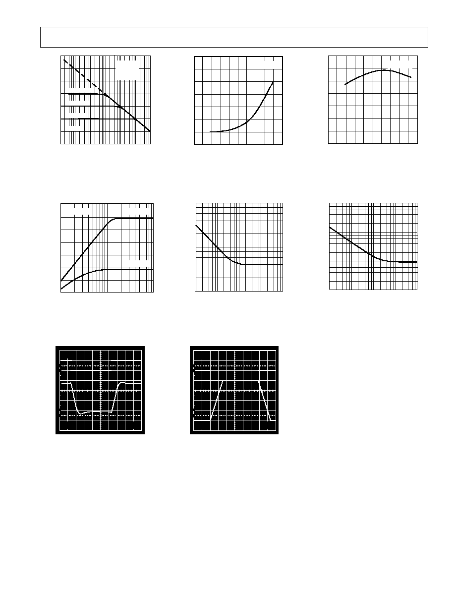
Typical Performance Characteristics≠OP420
150k
15k
1.5k
150
15
1.5
0.15
80
100
GAIN
≠
dB
V
S
= 15V
R
L
= 25k
T
A
= 25 C
A
VCL = 10
A
VCL = 1
FREQUENCY ≠ Hz
120
60
40
20
0
-20
A
VCL = 100
A
VCL = 1000
TPC 1. Closed-Loop Gain vs. Frequency
LOAD RESISTANCE ≠
PEAK OUTPUT
V
O
L
T
A
GE
≠
V
17
15
0
1k
10k
100k
10
5
V
S
= 15V
T
A
= 25 C
V
S
= -5V
TPC 4. Maximum Output Voltage
vs. Load Resistance
10
0%
100
90
20mV
2 s
50mV
TPC 7. Small-Signal Transient
Response
TEMPERATURE ≠ C
INPUT OFFSET CURRENT
≠
nA
700
-100
150
-50
0
50
100
V
S
= 15V
600
500
400
300
200
100
0
TPC 2. Input Offset Current vs.
Temperature
FREQUENCY ≠ Hz
INPUT V
O
L
T
A
GE
NOISE
DENISITY
≠
nV/
Hz
1000
100
10
0.1
1
1000
10
100
TPC 5. Input Voltage Noise Density
(e
n
) vs. Frequency
10
0%
100
90
5V
2V
200 s
TPC 8. Large-Signal Transient
Response
TEMPERATURE ≠ C
INPUT BIAS CURRENT
≠
nA
14
-100
150
-50
0
50
100
12
10
8
6
4
2
0
V
S
= 15V
TPC 3. Input Bias Current vs.
Temperature
FREQUENCY ≠ Hz
INPUT CURRENT NOISE DENSITY
≠
pA/
Hz
10
1.0
.01
0.1
1.0
1000
10
100
0.1
TPC 6. Input Current Noise Density
(i
n
) vs. Frequency
REV. A
OP420
≠6≠
OUTLINE DIMENSIONS
Dimensions shown in inches and (mm).
14-PIN HERMETIC DIP
14-PIN EPOXY DIP
14
1
7
8
0.310 (7.87)
0.220 (5.59)
PIN 1
0.098 (2.49) MAX
0.005 (0.13) MIN
0.100 (2.54) BSC
0.320 (8.13)
0.290 (7.37)
0.015 (0.38)
0.008 (0.20)
0.765 (19.94) MAX
SEATING
PLANE
0.023 (0.58)
0.014 (0.36)
0.060 (1.52)
0.015 (0.38)
0.200 (5.08)
MAX
0.200 (5.08)
0.125 (3.18)
0.070 (1.78)
0.030 (0.76)
0.150
(3.81)
MIN
16-PIN SOL
16
9
8
1
0.1574 (4.00)
0.1497 (3.80)
0.3937 (10.00)
0.3859 (9.80)
0.050 (1.27)
BSC
PIN 1
0.2440 (6.20)
0.2284 (5.80)
SEATING
PLANE
0.0098 (0.25)
0.0040 (0.10)
0.0192 (0.49)
0.0138 (0.35)
0.0688 (1.75)
0.0532 (1.35)
8
0
0.0196 (0.50)
0.0099 (0.25)
45
0.0500 (1.27)
0.0160 (0.41)
0.0099 (0.25)
0.0075 (0.19)
OP420CRC/883 20-LEAD LCC
TOP
VIEW
0.358 (9.09)
0.342 (8.69)
SQ
1
20
4
9
8
13
19
14
3
18
BOTTOM
VIEW
0.028 (0.71)
0.022 (0.56)
45 TYP
0.015 (0.38)
MIN
0.055 (1.40)
0.045 (1.14)
0.050 (1.27)
BSC
0.075 (1.91)
REF
0.011 (0.28)
0.007 (0.18)
R TYP
0.095 (2.41)
0.075 (1.90)
0.100 (2.54) BSC
0.200 (5.08)
BSC
0.150 (3.81)
BSC
0.075
(1.91)
REF
0.358
(9.09)
MAX
SQ
0.100 (2.54)
0.064 (1.63)
0.088 (2.24)
0.054 (1.37)
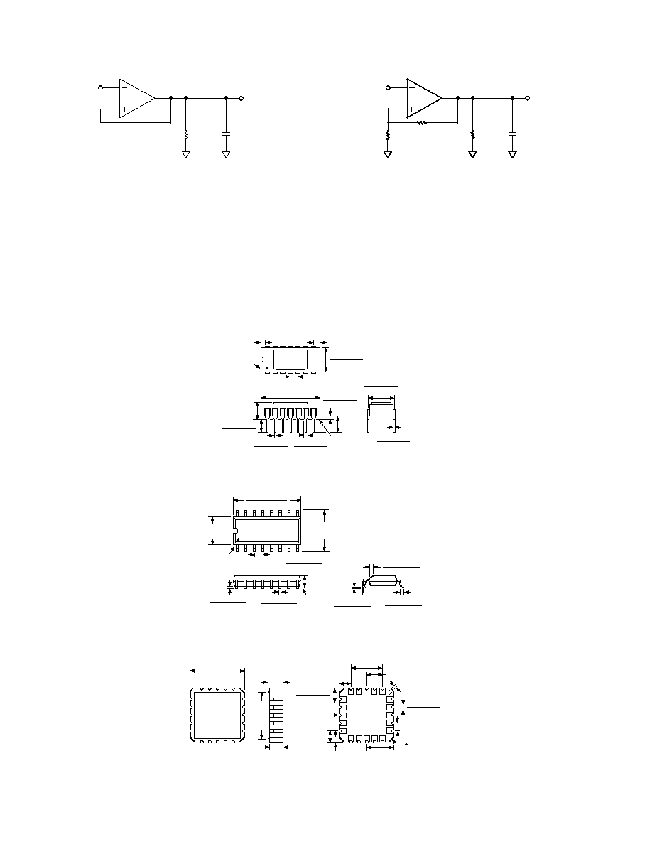
INPUT
OP420
R
L
25k
C
L
100k
OUTPUT
Figure 2. Small-Signal Transient Response
INPUT
OP420
R
L
25k
C
L
100pF
OUTPUT
10k
40k
Figure 3. Large-Signal Transient Response

REV. A
OP420
≠7≠
Revision History
Location
Page
11/01--Data Sheet changed from REV. 0 to REV. A.
Edits to GENERAL DESCRIPTION . . . . . . . . . . . . . . . . . . . . . . . . . . . . . . . . . . . . . . . . . . . . . . . . . . . . . . . . . . . . . . . . . . . . . . . . 1
Edits to ELECTRICAL CHARACTERISTICS . . . . . . . . . . . . . . . . . . . . . . . . . . . . . . . . . . . . . . . . . . . . . . . . . . . . . . . . . . . . . . 2, 3
Edits to ORDERING INFORMATION . . . . . . . . . . . . . . . . . . . . . . . . . . . . . . . . . . . . . . . . . . . . . . . . . . . . . . . . . . . . . . . . . . . . . . 4
Edits to ABSOLUTE MAXIMUM RATINGS . . . . . . . . . . . . . . . . . . . . . . . . . . . . . . . . . . . . . . . . . . . . . . . . . . . . . . . . . . . . . . . . . 4
Deleted DICE CHARACTERISTICS . . . . . . . . . . . . . . . . . . . . . . . . . . . . . . . . . . . . . . . . . . . . . . . . . . . . . . . . . . . . . . . . . . . . . . . 4
Deleted WAFER TEST LIMITS . . . . . . . . . . . . . . . . . . . . . . . . . . . . . . . . . . . . . . . . . . . . . . . . . . . . . . . . . . . . . . . . . . . . . . . . . . . 4

≠8≠
C00303≠0≠1/02(A)
PRINTED IN U.S.A.